Communication

All-Dielectric Dual-Band Metamaterial Absorber Based on Ring Nanocavity in Visible Region for Sensing Applications

1
School of Electronics and Information Engineering, Jinling Institute of Technology, Nanjing 211169, China
2
College of Photonic and Electronic Engineering, Fujian Normal University, Fuzhou 350007, China
3
Jiangsu Key Laboratory of Meteorological Observation and Information Processing, Nanjing University of Information Science and Technology, Nanjing 210044, China
4
School of Intelligent Control, Changzhou Institute of Industry Technology, Changzhou 213164, China
*
Author to whom correspondence should be addressed.
Photonics 2023, 10(1), 58; https://doi.org/10.3390/photonics10010058
Submission received: 13 November 2022 / Revised: 20 December 2022 / Accepted: 3 January 2023 / Published: 5 January 2023
(This article belongs to the Special Issue Nano/Micromechanical Metasurfaces and Active Metasurfaces/Plasmonics)

Abstract

:
In this study, an all-dielectric metamaterial absorber consisting of a ring nanocavity array, a spacer layer, and a metallic substrate is designed and investigated. The simulation results show that the two perfect absorption peaks (99.91% and 99.96%) are achieved at 539 nm and 673 nm. The two resonance modes caused by the different electric and magnetic field distributions of the ring nanocavity structure lead to different absorption and sensing properties. In addition, the influence of the structural parameters, such as the width of the nanocavity, on the sensing characteristics was studied and is presented here. A high sensitivity and narrow band result in a huge figure of merit when the proposed absorber is operated as a refractive index sensor.

1. Introduction

In recent years, metamaterials with a sub-wavelength structure received considerable attention from both the scientific and engineering communities because of their exotic electromagnetic properties [1,2]. Many applications, including high-sensitivity sensors [3,4,5], electromagnetic modulation devices [6,7], and perfect lenses [8] based on metamaterials rapidly developed. One of the most important and promising applications of metamaterial technology is as a perfect absorber due to its controllable absorption properties from the visible to microwave region [9,10,11,12,13,14]. Since the first metamaterial perfect absorber was reported by Landy in 2008 [15], various kinds of absorber were designed for different wavebands using metallic resonators [16,17,18]. However, the absorption performance, influenced by aspects such as the bandwidth and modulation range, is limited by the nonradiative ohmic losses on the metal surface. Thus, low-loss meta-optics and photonics are required for many cutting-edge applications [19]. As a replacement for lossy metal-based subwavelength photonics, the all-dielectric resonator platform based on high-index dielectric materials attracted much attention. Compared with their metallic counterparts, all-dielectric metamaterial absorbers are significantly efficient due to their lower losses, better modulation, and higher selective properties.
Due to their narrow bandwidth and perfect absorption, all-dielectric metamaterial absorbers are used as refractive index sensors. In the design and preparation of all-dielectric metamaterial refractive index sensors, terahertz [20,21] and infrared wavebands [22,23,24] are mainly focused on. Refractive index sensors based on metamaterial absorbers at visible frequencies are highly demanded. In particular, metamaterials based on silicon, which is the most important material in semiconductor devices and integrated circuit chips, are supported by mature semiconductor processing technology.
In this work, we designed and investigated a dual-band absorber based on all-dielectric structure, which can achieve perfect absorption in the visible region. The simulation results show that the dual-band absorber can yield an absorption coefficient over 99.9% at both resonance wavelengths. The electric and magnetic field distributions are calculated to understand the absorption mechanism at the resonance frequencies. In addition, the influence of structure parameters on the absorption and sensing performance is investigated, which can help in the optimization of structural parameters. The proposed dual-band absorber has high sensing characteristics, achieved by utilizing a simple structure.

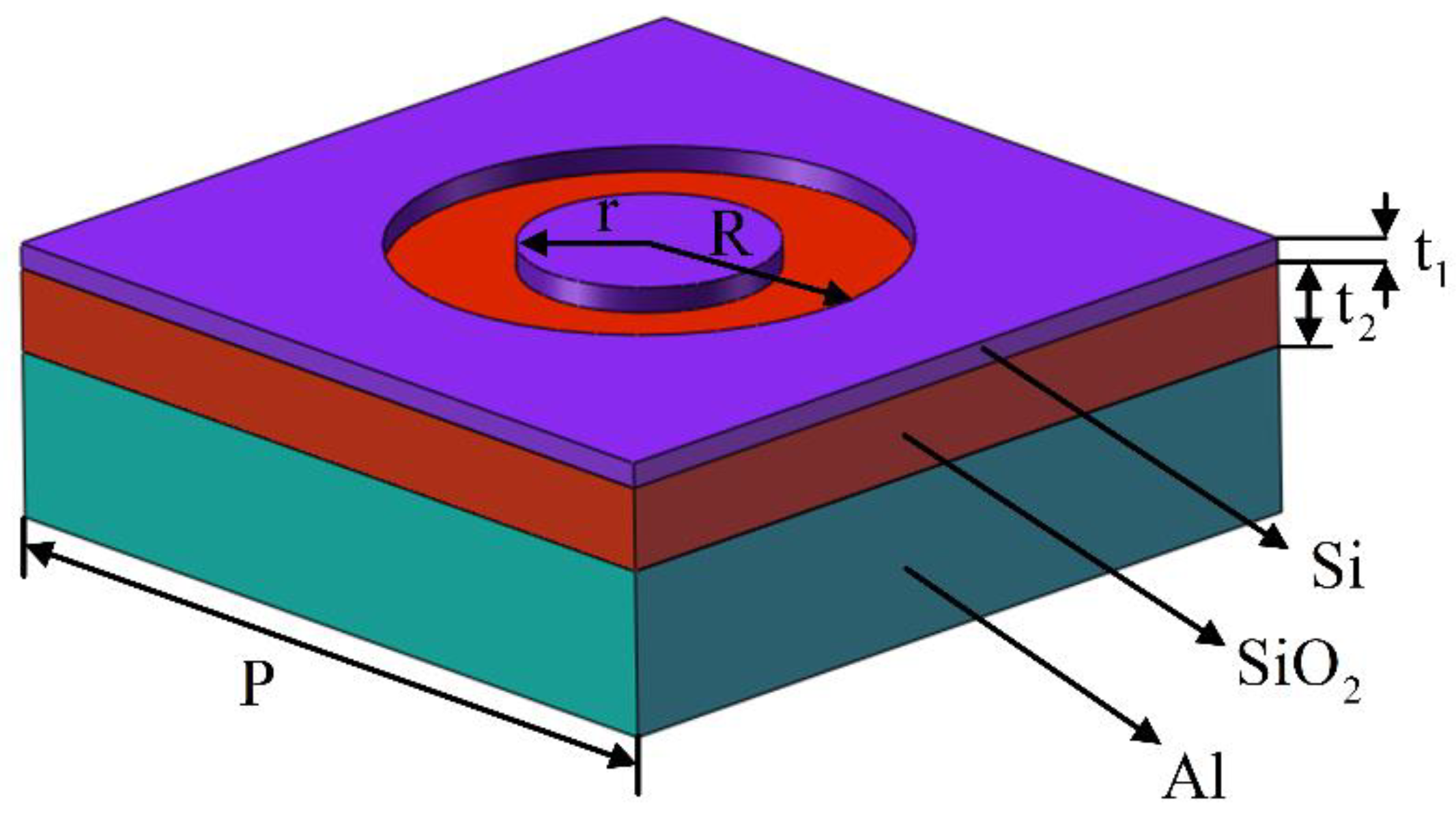
2. Materials and Structure

Figure 1 shows the structure of the designed absorber based on an all-dielectric two-dimensional (2D) photonic crystal. The elementary unit cell of the proposed absorber is formed by a three-layer structure consisting of a silicon layer decorated with a periodic array of a ring nanocavity, a SiO2 spacer layer, and an aluminum film as the metallic substrate. The optical cavities are arranged at the nodes of a square lattice with the lattice constant P. The outer and inner radii of the ring nanocavity are R and r, respectively. The thicknesses of the hollowed Si film and SiO2 layer are t1 and t2, respectively. The geometric parameters of the absorber were set as P = 500 nm, R = 120 nm, r = 60 nm, t1 = 10 nm, and t2 = 40 nm. The thickness of the bottom aluminum film is 100 nm. In addition, the surrounding material was set to air, and its refractive index is 1. The numerical simulation platform for our research relies on the FDTD method from the Lumerical software package algorithm.
In order to study the electromagnetic modulation properties of the designed absorber, the finite-difference time-domain (FDTD) software was used as a numerical simulation platform. The simulation results of the reflection and the transmission spectra are shown in Figure 2. When the light source is vertically incident, the reflectance of a metamaterial absorber is:
R = | Z Z 0 Z + Z 0 | 2
where Z0 is the free space impedance. Z is the effective impedance of the metamaterial absorber, which can be expressed as:
Z = ± ( 1 + S 11 ) 2 S 21 2 ( 1 S 11 ) 2 S 21 2
where S11 and S21 are the reflection and transmission coefficients, respectively. When the real and imaginary parts of the effective impedance are Re(Z) = 1 and Im(Z) = 0, respectively, the effective impedance of the metamaterial absorber matches the free-space impedance to achieve perfect absorption. Figure 2a shows the effective impedance of the metamaterial absorber with Re(Z) = 1 and Im(Z) = 0 at resonance points λ = 539 nm and 673 nm, matching the free space impedance. As shown in Figure 2b, the absorption spectrum can be calculated as A(λ) = 1-R(λ)-T(λ), where R(λ) and T(λ), respectively, represent the reflection spectra and the transmission spectra. Since the bottom aluminum film is opaque in the visible range, transmission is nearly close to zero, indicating the complete inhibition of transmission. Two absorption peaks were found at λ1 = 539 nm (peak 1) and λ2 = 673 nm (peak 2), and the peak absorptions reached 99.91% and 99.96%, respectively. In addition, the full width at half maximum (FWHM) values of the two absorption peaks are only 11 nm and 5 nm, respectively, and both exhibit extremely narrow linewidths of spectral absorption.

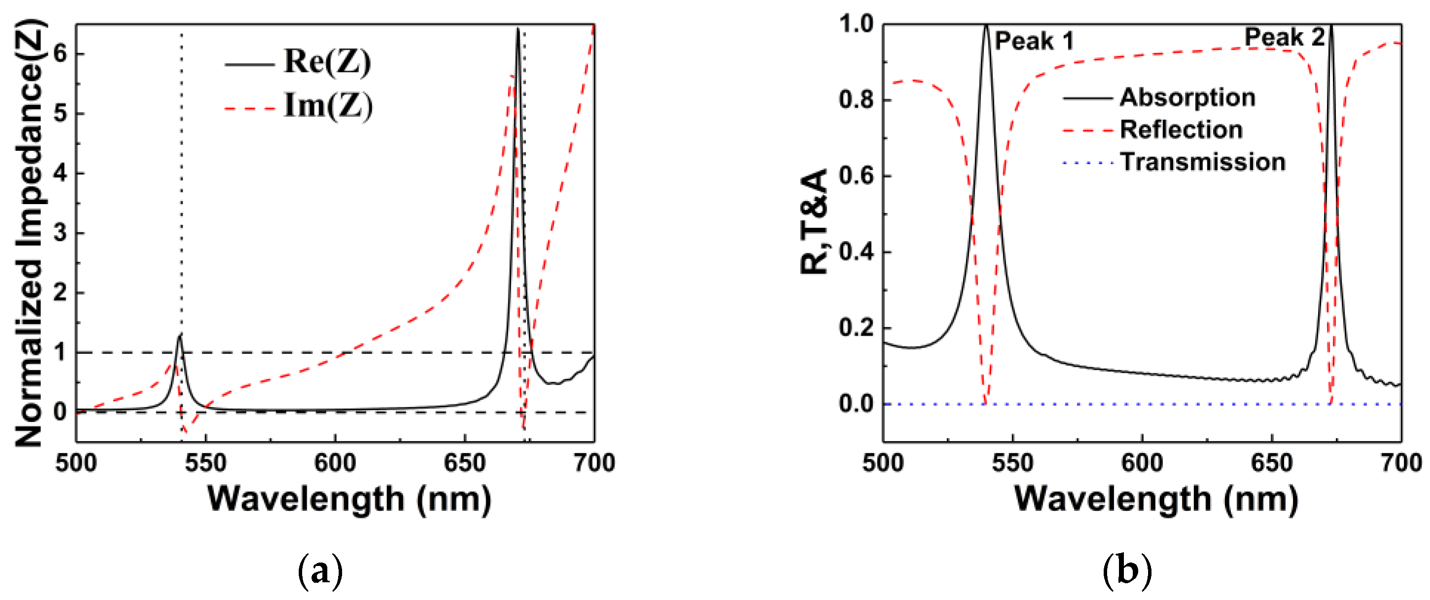
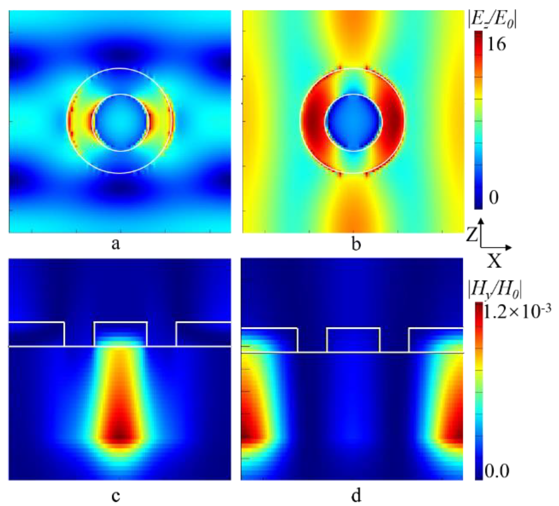
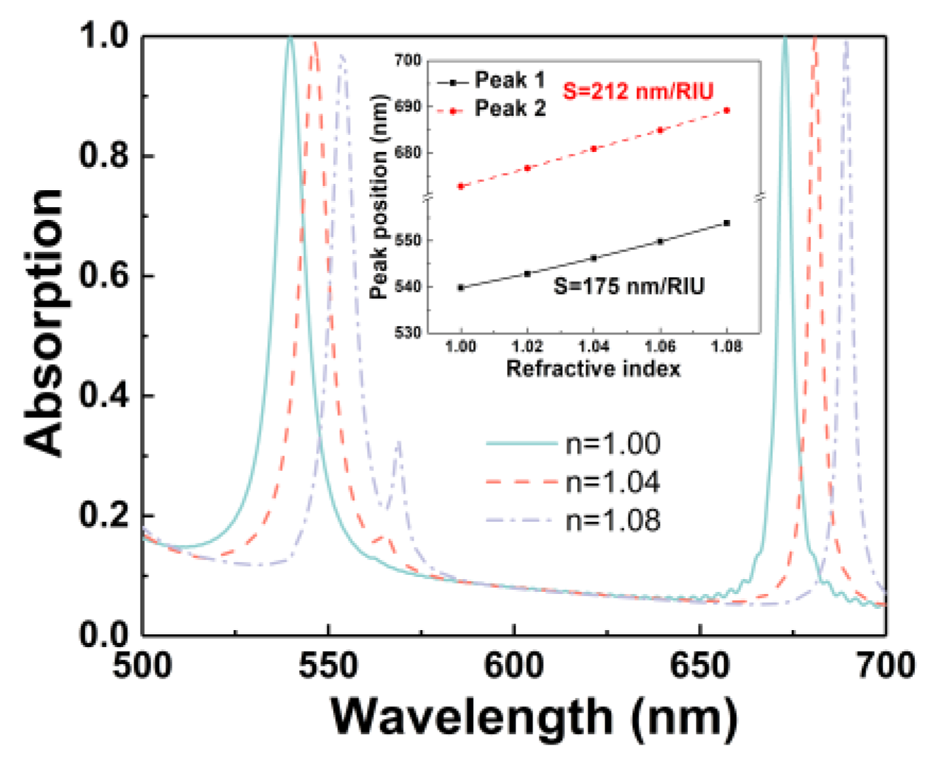
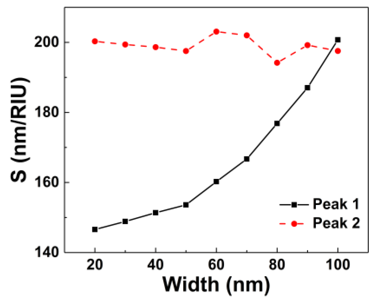
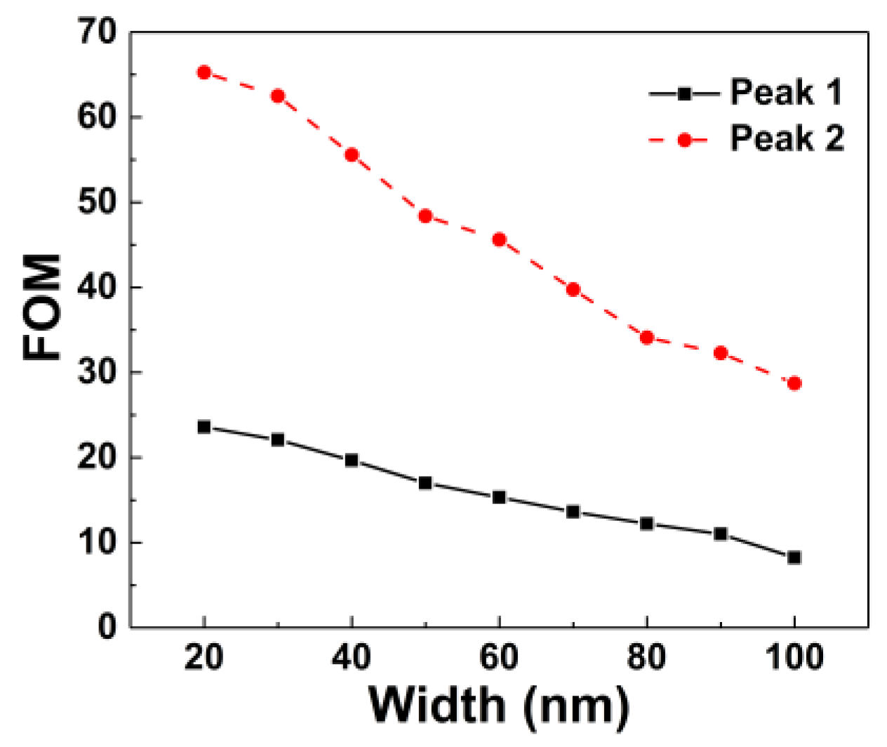
3. Results and Discussion

In order to better understand the dual-band absorption mechanism, the electric (|E|) field distributions at peak 1 (539 nm) and peak 2 (673 nm) were calculated and shown in Figure 3a,b, respectively. It is evident that the electric field at the resonant frequencies is strongly concentrated at the interface of ring nanocavity and the Si dielectric region [25]. The nanostructure presents very strong absorption at the visible realm, resulting in electric field enhancement of several orders of magnitude [26]. The electric field is localized at the interface of the ring nanocavity and Si dielectric region at peak 1, which indicates that the Mie-type resonant is excited by Si nanocylinders array, while the electric field is localized in the center of the ring nanocavity at peak 2, which indicates that the narrow band strong absorption can be attributed to the vertical gap plasmonic mode [24]. Figure 3c,d illustrates the simulated magnetic (|H|) field distributions of the proposed metamaterial absorber at the resonance wavelengths. At peak 1, the magnetic intensity is distributed under the Si nanocylinder, as shown in Figure 3c, which presents high-index dielectric (such as Si) nanoparticles supporting strong Mie-like geometrical resonances in the visible spectral range [25], whereas the magnetic intensity distribution at peak 2 is localized between the periodic ring nanocavity, indicating that the resonant is excited by the incident waves coupled with the periodic ring nanocavity structure.
To better understand the absorption mechanism of the all-dielectric structure, the influences of the width (w = R − r) of the ring nanocavity on the absorption spectrum are investigated. Figure 4a shows the dependence of the absorption spectrum on the change in the width, and Figure 4b shows the value of FWHM as a function of the width. As shown in Figure 4a, both the absorption rates of peaks 1 and 2 become bigger first then smaller later as the width increases. The peak absorption rates of both peaks are higher than 90% when the width is from 40 nm to 80. In addition, the position of peaks 1 and 2 blue shift as w increases. The resonant wavelength is sensitive to the width of the ring nanocavity at peak 1, which blueshifts from 547 nm to 532 nm as the width is increased from 40 nm to 80 nm. By contrast, the position of peak 2 blueshifts from 676 nm to 668 nm under the same conditions. The origin of the blueshift can be discussed by an equivalent inductor–capacitor (LC) circuit. The Si nanocylinder and the dielectric layer across the nanocavity were considered as gap capacitors whose capacitance C can be approximately defined by a plate capacitor form as C = ε0εrσeff/w, where ε0 is the permittivity of vacuum, εr is the real part of the relative permittivity of the nanocavity, and σeff is the effective area of dielectric across the nanocavity. Obviously, C will decrease as w increases, which will then lead to a decreased resonance wavelength (blue shift) at the resonant peak. The relation of the FWHM and the width was also investigated through numerical calculations, as seen in Figure 4b. The FWHM value of the first resonant mode (peak 1) shows an exponential increase as a function of the width. When the width increases from 20 nm to 100 nm, the value of FWHM increases rapidly from 6 nm to 21 nm. For the resonant mode of peak 2, the non-linearity of the variation is weak, such that a linear approximation is possible over the whole range of the width, and the FWHM can be as narrow as 3.2 nm.
For sensing applications, the resonant wavelengths of the designed metamaterial absorber are dependent on the refractive index of the surrounding dielectric environment. The influence of the refractive index on absorption properties can be explained by the change in the capacitance of the structure. The relationship of the refractive index n and dielectric constant ε is expressed as n = ε1/2. The capacitance C of the equivalent inductor—capacitor (LC) circuit can be expressed as C = ε0n2σeff/w. When the refractive index of the surrounding media increases, the capacitance value increases due to the dielectric constant, and the resonances redshift towards a longer wavelength. In order to ensure a good sensor performance of the all-dielectric metamaterial absorber, the refractive index range was set from 1.00 to 1.08 in intervals of 0.02. As seen in Figure 5, the resonance wavelength shift, which is directly connected to the sensitivity of the metamaterial sensor, is plotted as a function of the refractive index. With an increase in the refractive index, the resonance wavelength shift increases linearly. The slopes of the fitting curves were used to evaluate the sensitivity of the sensor as S = dλ/dn, where dλ is the resonance wavelength shift and dn is the change in the refractive index. The value of S reaches about 175 nm/refractive index unit (RIU) for the first resonant mode and 212 nm/RIU for the second resonant mode (the inset in Figure 5).
In order to investigate the influence of structural parameters of the all-dielectric absorber on the sensor properties, we simulated the sensitivity of the sensor while changing the width of ring nanocavity. As shown in Figure 6, the values of sensitivity vary with the width of the ring cavity from 20 nm to 100 nm. Due to the different plasmonic modes, the two absorption peaks respond differently to the perturbation of the neighboring medium refractive index. For peak 1, the relation between the values of sensitivity and the width of the ring cavity is the opposite of the Figure 4b. When the width increases from 20 nm to 100 nm, the value of the sensitivity at peak 1 increases rapidly with the width. Meanwhile, the value of S at peak 2 is very stable and stayed at about 200 nm/RIU.
Absorption peaks with narrow line widths are useful in detection of the resonance wavelength shift by changing the refractive index. Figure of merit (FOM), which is determined by the sensitivity (S) and the FWHM as S/FWHM, is a more significant factor when estimating sensor quality and allows a direct comparison of sensing performance among different sensors [25]. The FOMs of each absorption peak, which varied with the width of the ring nanocavity from 20 nm to 100 nm, were calculated and are shown in Figure 7. The FOM parameters of peak 1 and peak 2 show the identical patterns when the width is changed. With a decrease in width, the FOM of peak 1 increases from 8.2 to 23.6, while the FOM of peak 2 can reach a higher value (65.3) due to its narrower band, as shown in Figure 4b.
For the comparison of the plasmonic properties of many different senses, figure of merit, in the generalized form introduced by J. Becker, is denoted as [27]:
FOM * = ( d I / I d n ) M A X
where dI/I is the change in relative intensity, and dn is the change in refractive index. The resonant wavelength at the perfect absorption peak was chosen such that the reflection intensity is near zero and FOM* is at its maximum value. The proposed dual-band absorber can yield an extremely big value, FOM* = 17,265 and 59,902 at the resonance wavelengths of 539 nm and 673 nm, respectively.
Operated frequency region, absorption peak number, absorption rate, FOM, and FOM* are some important features that can be used to distinguish the refractive index sensor based on a metamaterial absorber. Compared with the refractive index sensors as previously reported in recent years (see Table 1), the dual-band metamaterial perfect absorber based on an all-dielectric nanocavity for sensing applications as presented in this paper has some important significance. Firstly, the simple all-dielectric structure, as the replacement for the MIM sandwich structure, can definitely alleviate the difficulty faced in the design and fabrication process. Secondly, the higher absorption coefficient over 99.9% at both of the two resonance frequencies is among the best values despite of the compared metamaterial absorbers in Table 1. In addition, the proposed refractive index sensor has a higher FOM and FOM* than some of these published absorbers. At last, the proposed absorber can work in the visible region, which is still highly demanded in many applications.

4. Conclusions

In summary, we proposed a dual-band metamaterial perfect absorber based on an all-dielectric structure as a refractive index sensor, consisting of a silicon-based ring nanocavity array, a SiO2 layer, and aluminum film. The electromagnetic response characteristics of the absorber were theoretically and numerically studied. The dual-band perfect absorptions (99.91% and 99.96%) were achieved at resonance wavelengths of 539 nm and 673 nm. The FWHM, sensitivity, FOM, and FOM* for the metamaterial sensor were calculated from the two absorption peaks as a function of the width of the ring nanocavity. The proposed all-dielectric absorber shows many advantages for refractive index sensors applied in the visible region due to the high sensitivity (~200 nm/RIU), FOM (65.3), and FOM* (59,902) at its two absorption peaks.

Author Contributions

Conceptualization, F.L. and B.N.; formal analysis, F.L., M.Z. and Z.F.; funding acquisition, F.L., Y.W. and B.Y.; writing, F.L. All authors have read and agreed to the published version of the manuscript.

Funding

This research was funded by the General project of Natural Science Foundation of colleges and universities of Jiangsu Province (19KJD470001) and the National Natural Science Foundation of China, Grant numbers 61904071 and 22004052.

Institutional Review Board Statement

Not applicable.

Informed Consent Statement

Not applicable.

Data Availability Statement

The data presented in this study are available on request from the corresponding author.

Conflicts of Interest

The authors declare no conflict of interest.

References

  1. Yan, X.T.; Tang, W.; Liu, J.F.; Wang, M.; Gao, X.X.; Cui, T.J. Glide symmetry for mode control and significant suppression of coupling in dual-strip SSPP transmission lines. Adv. Photonics 2021, 3, 026001. [Google Scholar] [CrossRef]
  2. Xu, Z.; Chang, J.; Tong, J.; Sievenpiper, D.F.; Cui, T.J. Near-field chiral excitation of universal spin-momentum locking transport of edge waves in microwave metamaterials. Adv. Photonics 2022, 4, 046004. [Google Scholar] [CrossRef]
  3. Ma, T.; Huang, Q.; He, H.; Zhao, Y.; Lin, X.; Lu, Y. All-dielectric metamaterial analogue of electromagnetically induced transparency and its sensing application in terahertz range. Opt. Express 2019, 27, 16624–16634. [Google Scholar] [CrossRef] [PubMed]
  4. Liu, N.; Mesch, M.; Weiss, T.; Hentschel, M.; Giessen, H. Infrared Perfect Absorber and Its Application as Plasmonic Sensor. Nano Lett. 2010, 10, 2342–2348. [Google Scholar] [CrossRef] [PubMed]
  5. Tong, L.; Wei, H.; Zhang, S.; Xu, H. Recent Advances in Plasmonic Sensors. Sensors 2014, 14, 7959–7973. [Google Scholar] [CrossRef] [PubMed] [Green Version]
  6. Xu, W.-Z.; Ren, F.-F.; Ye, J.; Lu, H.; Liang, L.; Huang, X.; Liu, M.; Shadrivov, I.V.; Powell, D.A.; Yu, G.; et al. Electrically tunable terahertz metamaterials with embedded large-area transparent thin-film transistor arrays. Sci. Rep. 2016, 6, 23486. [Google Scholar] [CrossRef] [PubMed] [Green Version]
  7. Xu, W.-Z.; Shi, Y.-T.; Ye, J.; Ren, F.-F.; Shadrivov, I.V.; Lu, H.; Liang, L.; Hu, X.; Jin, B.; Zhang, R.; et al. A terahertz Controlled-NOT gate based on asymmetric rotation of polarization in chiral metamaterials. Adv. Opt. Mater. 2017, 5, 1700108. [Google Scholar] [CrossRef]
  8. Ramm, A. Does negative refraction make a perfect lens? Phys. Lett. A 2008, 372, 6518–6520. [Google Scholar] [CrossRef] [Green Version]
  9. Cui, T.J. Microwave metamaterials—From passive to digital and programmable controls of electromagnetic waves. J. Opt. 2017, 19, 084004. [Google Scholar] [CrossRef]
  10. Wang, X.; Ding, W.; Zhu, H.; Liu, C.; Liu, Y. Tunable broadband, wide-angle, and polarization-dependent perfect infrared absorber based on planar structure containing phase-change material. Appl. Opt. 2018, 57, 8915–8920. [Google Scholar] [CrossRef]
  11. Kajtár, G.; Kafesaki, M.; Economou, E.; Soukoulis, C.M. Theoretical model of homogeneous metal–insulator–metal perfect multi-band absorbers for the visible spectrum. J. Phys. D Appl. Phys. 2016, 49, 055104. [Google Scholar] [CrossRef]
  12. Norouzi-Razani, A.; Rezaei, P. Broadband polarization insensitive and tunable terahertz metamaterial perfect absorber based on the graphene disk and square ribbon. Micro Nanost. 2022, 163, 107153. [Google Scholar] [CrossRef]
  13. Qing, Y.M.; Ma, H.F.; Cui, T.J. Tailoring anisotropic perfect absorption in monolayer black phosphorus by critical coupling at terahertz frequencies. Opt. Express 2018, 26, 32442–32450. [Google Scholar] [CrossRef] [PubMed]
  14. Liu, F.; He, M.; Dong, Z.; Wang, Y.; Ni, B. Design of tunable dual-band terahertz perfect absorber base on graphene. Results Phys 2022, 40, 105860. [Google Scholar] [CrossRef]
  15. Landy, N.I.; Sajuyigbe, S.; Mock, J.J.; Smith, D.R.; Padilla, W.J. Perfect metamaterial absorber. Phys. Rev. Lett. 2008, 100, 207402. [Google Scholar] [CrossRef] [PubMed]
  16. Xu, L.; Shen, Y.; Gu, L.; Li, Y.; Deng, X.; Wei, Z.; Xu, J.; Cao, J. Optical strong coupling in hybrid metal-graphene metamaterial for terahertz sensing*. Chin. Phys. B 2021, 30, 118702. [Google Scholar] [CrossRef]
  17. Li, G.; Shen, Y.; Xiao, G.; Jin, C. Double-layered metal grating for high-performance refractive index sensing. Opt. Express 2015, 23, 8995–9003. [Google Scholar] [CrossRef]
  18. Si, J.N.; Dong, Z.W.; Yu, X.Y.; Deng, X.X. Tunable polarization-independent dual-band coherent perfect absorber based on metal-graphene nanoring structure. Opt. Express 2018, 26, 21768–21777. [Google Scholar] [CrossRef]
  19. Cole, M.A.; Powell, D.A.; Shadrivov, I.V. Strong terahertz absorption in all-dielectric Huygens’ metasurfaces. Nanotechnology 2016, 27, 424003. [Google Scholar] [CrossRef]
  20. Zhong, Y.; Du, L.; Liu, Q.; Zhu, L.; Meng, K.; Zou, Y.; Zhang, B. Ultrasensitive specific sensor based on all-dielectric metasurfaces in the terahertz range. RSC Adv. 2020, 10, 33018–33025. [Google Scholar] [CrossRef]
  21. Wang, Y.; Han, Z.; Du, Y.; Qin, J. Ultrasensitive terahertz sensing with high-Q toroidal dipole resonance governed by bound states in the continuum in all-dielectric metasurface. Nanophotonics 2021, 10, 1295–1307. [Google Scholar] [CrossRef]
  22. Ye, J.; Van Dorpe, P. Improvement of Figure of Merit for Gold Nanobar Array Plasmonic Sensors. Plasmonics 2011, 6, 665–671. [Google Scholar] [CrossRef]
  23. Ye, H.-Y.; Huang, X.-Q.; Wen, K.-H.; Xue, J.-C.; Zhou, J.-Y.; Meng, Z.-M. Near-infrared narrow plasmonic resonances for high-performance optical sensing in a sodium-based nanograting. Results Phys. 2022, 38, 105566. [Google Scholar] [CrossRef]
  24. Danilov, A.; Tselikov, G.; Wu, F.; Kravets, V.G.; Ozerov, I.; Bedu, F.; Grigorenko, A.N.; Kabashin, A.V. Ultra-narrow surface lattice resonances in plasmonic metamaterial arrays for biosensing applications. Biosens. Bioelectron. 2018, 104, 102–112. [Google Scholar] [CrossRef] [Green Version]
  25. Huang, L.; Xu, L.; Mohsen, R. Pushing the limit of high-Q mode of a single dielectric nanocavity. Adv. Photonics 2021, 3, 16004. [Google Scholar] [CrossRef]
  26. Bozhevolnyi, S.I.; Sondergaard, T. General properties of slow-plasmon resonant nanostructures: Nano-antennas and resonators. Opt. Express 2007, 15, 10869–10877. [Google Scholar] [CrossRef]
  27. Becker, J.; Trügler, A.; Jakab, A.; Hohenester, U.; Sönnichsen, C. The Optimal Aspect Ratio of Gold Nanorods for Plasmonic Bio-sensing. Plasmonics 2010, 5, 161–167. [Google Scholar] [CrossRef]
  28. Xie, Q.; Dong, G.; Wang, B.-X.; Huang, W.-Q. Design of Quad-Band Terahertz Metamaterial Absorber Using a Perforated Rectangular Resonator for Sensing Applications. Nanoscale Res. Lett. 2018, 13, 137. [Google Scholar] [CrossRef] [Green Version]
  29. Lu, X.; Zhang, L.; Zhang, T. Nanoslit-microcavity-based narrow band absorber for sensing applications. Opt. Express 2015, 23, 20715–20720. [Google Scholar] [CrossRef]
  30. Yong, Z.; Zhang, S.; Gong, C.; He, S. Narrow band perfect absorber for maximum localized magnetic and electric field enhancement and sensing applications. Sci. Rep. 2016, 6, 24063. [Google Scholar] [CrossRef]
  31. Liu, Z.; Liu, G.; Fu, G.; Liu, X.; Huang, Z.; Gu, G. All-metal meta-surfaces for narrowband light absorption and high performance sensing. J. Phys. D Appl. Phys. 2016, 49, 445104. [Google Scholar] [CrossRef]
  32. Li, Y.; An, B.; Jiang, S.; Gao, J.; Chen, Y.; Pan, S. Plasmonic induced triple-band absorber for sensor application. Opt. Express 2015, 23, 17607–17612. [Google Scholar] [CrossRef] [PubMed]
  33. Huang, X.; Zhang, B.; Wang, Y.; Zhu, M.; Shao, G. Reduced resonance line-width and enhanced figure of merit in Ag/Si/SiO2 nanopillar array sensors. Results Phys. 2020, 19, 103612. [Google Scholar] [CrossRef]
Figure 1. The elementary unit cell of the proposed structure.
Photonics 10 00058 g001
Figure 2. (a) Normalize impedance of the proposed absorber. (b) Reflection, transmission, and absorption spectrum.
Photonics 10 00058 g002
Figure 3. (a) Electric field diagram at λ1 = 539 nm; (b) electric field diagram at λ2 = 673 nm in XY plane; (c) magnetic field diagram at λ1 = 539 nm; and (d) magnetic field diagram at λ2 = 673 nm in XZ plane.
Photonics 10 00058 g003
Figure 4. (a) Absorption spectrum for different width of nanocavity. (b) The relation between FWHM of absorption peak and width.
Photonics 10 00058 g004
Figure 5. Absorption spectrum for a different background refractive index. Inset: the spectral position as a function of the background refractive index.
Photonics 10 00058 g005
Figure 6. The relation between sensitivity and width of ring nanocavity.
Photonics 10 00058 g006
Figure 7. The relation between FOM and width of nanocavity.
Photonics 10 00058 g007
Table 1. Comparison of the proposed absorber with the published refractive index sensors.
ReferencesWavelength
Region
Peak NumbersPeak
Absorption (%)
FOMFOM*
[28]THz160.86101-
[29]Infrared19525322
[30]Infrared199.611019,000
[31]Infrared289501075
[32]Visible3>99~5545,367
[33]Visible2~6064.3-
The workVisible299.91,
99.96
23.6
65.3
17,265
59,902
Disclaimer/Publisher’s Note: The statements, opinions and data contained in all publications are solely those of the individual author(s) and contributor(s) and not of MDPI and/or the editor(s). MDPI and/or the editor(s) disclaim responsibility for any injury to people or property resulting from any ideas, methods, instructions or products referred to in the content.

