Article

Analysis of Multi-Stacked Dielectric Resonator Antenna with Its Equivalent R-L-C Circuit Modeling for Wireless Communication Systems

by
Ram Krishna
1,2,*,
Agbotiname Lucky Imoize
3,4,*,
Rajveer Singh Yaduvanshi
5,
Harendra Singh
2,
Arun Kumar Rana
6 and
Subhendu Kumar Pani
7
1
Department of Electronics and Communication Engineering, Ambedkar Institute of Advanced Communication Technologies and Research (AIACTR), Guru Gobind Indraprastha University (GGSIPU), Delhi 110031, India
2
Department of Electronics and Communication Engineering, G. L. Bajaj Institute of Technology and Management, Greater Noida 201306, India
3
Department of Electrical and Electronics Engineering, Faculty of Engineering, University of Lagos, Akoka, Lagos 100213, Nigeria
4
Department of Electrical Engineering and Information Technology, Institute of Digital Communication, Ruhr University, 44801 Bochum, Germany
5
Department of Electronics and Communication Engineering, Netaji Subhas University of Technology (NSUT), Delhi 110078, India
6
Department of Computer Science, Galgotias College of Engineering of Technology, Greater Noida 201310, India
7
Krupajal Engineering College, Biju Patnaik University of Technology (BPUT), Bhubaneswar 751002, India
*
Authors to whom correspondence should be addressed.
Math. Comput. Appl. 2023, 28(1), 4; https://doi.org/10.3390/mca28010004
Submission received: 7 November 2022 / Revised: 16 December 2022 / Accepted: 23 December 2022 / Published: 29 December 2022

Abstract

:
The dielectric resonator antenna (DRA) can be modeled as a series and parallel combination of electrical networks consisting of a resistor (R), inductor (L), and capacitor (C) to address peculiar challenges in antennas suitable for application in emerging wireless communication systems for higher frequency range. In this paper, a multi-stacked DRA has been proposed. The performance and characteristic features of the DRA have been analyzed by deriving the mathematical formulations for dynamic impedance, input impedance, admittance, bandwidth, and quality factor for fundamental and high-order resonant modes. Specifically, the performance of the projected multi-stacked DRA was analyzed in MATLAB and a high-frequency structure simulator (HFSS). Generally, results indicate that variation in the permittivity of substrates, such as high and low, can potentially increase and decrease the quality factor, respectively. In particular, the impedance, radiation fields and power flow have been demonstrated using the proposed multi-stacked electrical network of R, L, and C components coupled with a suitable transformer. Overall, the proposed multi-stacked DRA network shows an improved quality factor and selectivity, and bandwidth is reduced reasonably. The multi-stacked DRA network would find useful applications in radio frequency wireless communication systems. Additionally, for enhancing the impedance, BW of DRA a multi-stacked DRA is proposed by the use of ground-plane techniques with slots, dual-segment, and stacked DRA. The performance of multi-stacked DRA is improved by a factor of 10% as compared to existing models in terms of better flexibility, moderate gain, compact size, bandwidth, quality factor, resonant frequency, frequency impedance at the resonance frequency, and the radiation pattern with Terahertz frequency range.

1. Introduction

Mathematical modeling is the basic requirement for the designing analysis of any antenna. To understand and analyze the performance characteristics of that antenna, a stacked R-L-C network is used [1]. The present article proposes HFSS multi-stacked DRA modeling utilizing an equivalent circuit design strategy [2]. The mathematical modelling of an equivalent R-L-C network has been explained in detail [3]. This explains how the main mode spreads using an aperture-coupled slot to form an equivalent transmission line. The functions from source to endpoints have been precisely expressed by the lumped impedances. The radiated waves in space are displayed by the reactance that controls the reactive power brought on by feed, termination, and resistances. The proposed methodology can be utilized to calculate the input impedance of aperture-coupled loading multi-stacked DRA [4]. Very little research has been done on modeling multi-stacked DRA equivalent circuits till now, however, there is already a substantial amount of related work on patch antenna equivalent circuits [5]. The proposed circuit illustration yields positive results for the internal impedance and loads of multiple stacked DRAs. The multi-stacked DRAs impedances and radiation fields have been modelled using higher order and fundamental modes. An equivalent circuit model was used to represent the circuit bandwidth, resonance, and other radiation field parameters. This approach is also helpful to develop higher-order models accurately. The radiation patterns and other field behaviors of multi-stacked DRA can be predicted using the suggested method and resonant mode circuit models [6]. The presented research work accurately develops a simple and absolute ‘physics-based’ circuit for resonant modes. The equivalent circuit model can extrapolate the resonance parameters, such as bandwidth, quality factor, resonant frequency, frequency impedance at the resonance frequency, and the radiation pattern of multi-stacked DRA [7]. The different multi-stacked DRA structures can be designed and analyzed using HFSS and MATLAB software. The proposed concept of resonant simplifies the designing of multi-stacked DRAs. This method of analysis has linked the multi-stacked DRA circuit models to their radiated fields for the first time in a multi-stacked DRA study [8].
Since its initial debut in 1983, dielectric resonator antennas (DRA) have undergone substantial research. DRAs have several key characteristics that set them apart from other types of antennas, including ease of excitation, fairly wide bandwidths, and small size. In this presented work, a multi-stacked parallel RLC circuit-based dielectric resonant antenna has been proposed with a good amount of improvement in bandwidth, quality factor, resonant frequency, frequency impedance at the resonance frequency, and the radiation pattern in the Terahertz frequency range. A cooperative 6G-based optimized simultaneous wireless information and power transfer (SWIPT) system for two-user pairing in terahertz was created by Oleiwi et al. [9]. When SIC manipulation is used to examine the model’s performance, the results show that the suggested system performs 75% better in terms of energy and spectral efficiency than more traditional models, such as NOMA and OMA, time division multiple access (TDMA). Kremer et al. [10] proposed a dielectric resonant antenna (DRA) for high frequency. The broadside radiation of the proposed DRA has an impedance bandwidth of 21.6% and an axial ratio bandwidth of 16.7%. A cylindrical segmented dielectric resonator antenna (CDRA) with three distinct (120°, 60°, 300°) segments and cylindrical radius r 1 ,   r 2 and r 3 with stacking angular displacement was proposed by Chauhan and Mukherjee [11]. The proposed antenna has an impedance bandwidth of 90% (3.3 GHz to 8.7 GHz) and an axial ratio bandwidth of 53.8% (3.8 GHz-6.6 GHz) and 58.5% (3.5 GHz–6.4 GHz), respectively, according to simulation and measurement. Oleiwi [12] has created a SWIPT-pairing system for cooperative H-NOMA in 6G Terahertz communications. The proposed THz frequency ranges for combining hybrid non-orthogonal multiple access (H-NOMA) and cooperative simultaneous wireless information and power transmission (SWIPT) (H-NOMA). The energy and spectral efficiency of the multilateral recommended system is 75% higher than that of the related work. Gupta et al. [13] proposed a Low profile multilayer cylindrical segment fractal DRA for wideband applications. Although the author offered different multilayer cylindrical DRA structures, the stacked DRA, dual-segment, hybrid DRA, and slots in ground-plane approaches were also well suited to improving the impedance BW of DRA. Fractal applications’ primary goal is to lower the antenna’s size for wideband characteristics while keeping other design parameters within reasonable bounds. Wang et al. [14] proposed an ultra-wideband dielectric resonator antenna (DRA). In essence, it achieves a relative bandwidth of 90.9% and covers the frequency range from 6 GHz to 16 GHz. The antenna array’s operational frequency range is 5.42 GHz to 16.5 GHz, with a 101.1% relative bandwidth. Within the operational frequency band, a large scanning angle of 60 is obtained, with a good scanning pattern and cross-polarization. Chauhan and Mukherjee [15] a high gain fractal cylindrical DRA for UWB application with 120°, 60°, 300° an angular portion of a cylinder with a radius ratio (1:2:3). The proposed structure offers an operating bandwidth of 9.2 GHz and spans from 3.6 GHz–12.8 GHz. The suggested antenna has a maximum gain of 9.45 dB and an efficiency of more than 89%, making it appropriate for satellite communication.
The main motive for to design and analysis of the proposed rectangular-shaped multi-staked DRA is to improve the quality factor and selectivity, decrease the bandwidth, and reduce the physical structure, design cost, improve flexibility, and moderate gain. Multiple DRAs using parallel R, L, and C components are coupled by using L & C components are used to design the rectangular antenna. The main contributions of the proposed article are:
  • Understanding and analyzing antenna performance characteristics using a stacked R-L-C network. The multi-stacked DRA used in this paper was designed and examined using HFSS and MATLAB tools;
  • This describes how the main mode propagates as an equivalent transmission line using an aperture-coupled slot. The reactance responsible for the reactive power due to feed, termination, and resistances exactly shows the radiated waves in space. The proposed circuit illustration yields positive results for the internal impedance and loads of multiple stacked DRAs;
  • An equivalent circuit model was used to represent the circuit bandwidth, resonance, and other radiation field parameters. Multi-stacked radiation patterns and other field behaviors can be predicted using the suggested method and resonant mode circuit models;
  • The presented research work accurately develops a simple and absolute ‘physics-based’ circuit for resonant modes. The equivalent circuit model can extrapolate the resonance parameters, such as bandwidth, quality factor, resonant frequency, frequency impedance at the resonance frequency, and the radiation pattern of multi-stacked DRA.

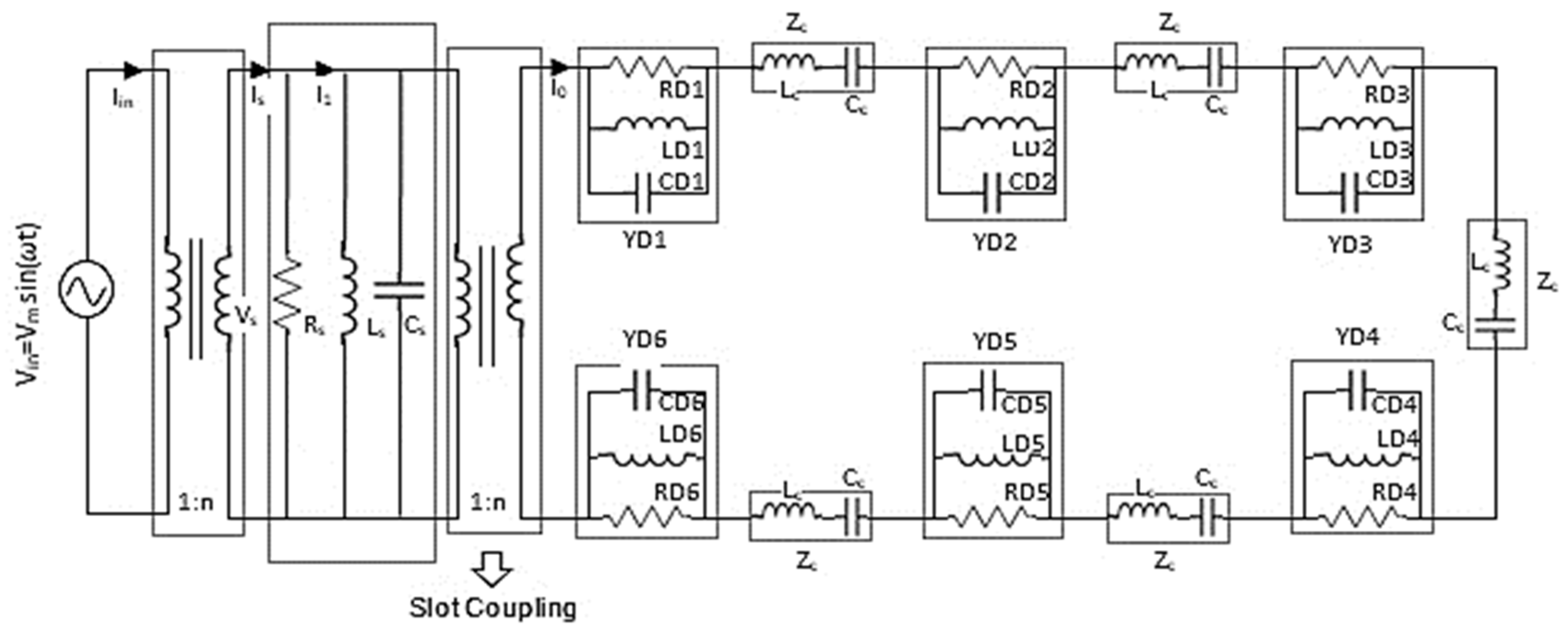
2. Proposed Methodology for Designing of Multi-Stacked DRA

A multi-stacked dielectric resonator antenna (MSDRA) with its equivalent R-L-C circuit, shown in Figure 1, is proposed for mathematical modeling as well as analysis point of view [16,17]. The solution of multi-stacked DRA equivalent circuit with electrical element resistor, inductor, and capacitor in shunt circuit for current i 0 (t), resonant frequency ( f r ), Dynamic impedance (Zd), input impedance (Zin), Quality factor, and bandwidth (BW) have been worked. The simplified equivalent circuit of multi-stacked DRA is shown in Figure 2.

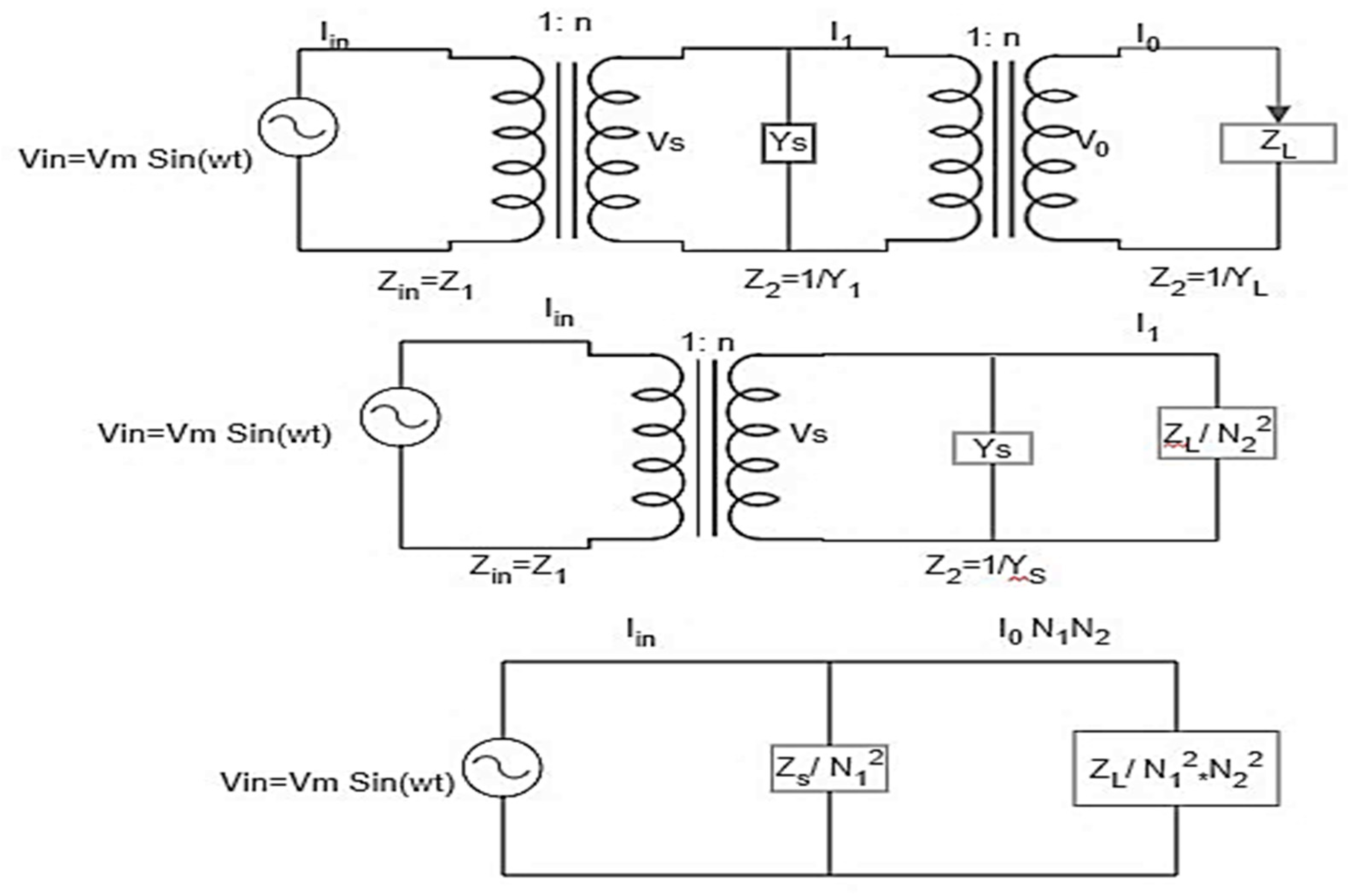
2.1. Multi-Stacked DRA Impedance (ZL)

To calculate the mathematical expression of the input impedance of a multi-stacked DRA, individual admittance and impedance of each DRA are connected in cascade and the impedance transformation concept of transformer is used, as shown below [18,19];
Individual admittance of each DRA:
Y d i s = 1 R d i + s c d i + 1 s L d i
Individual coupling impedance between DRA:
Z C i = s L C i + 1 s C C i
Total load impedance of Multi-stacked DRA:
Z L   = 1 Y d i + Z c i = Z d i + Z c i
where the value of i changes from 1 to 6.
Slot admittance of Multi-stacked DRA:
Y s s = 1 R s + s c s + 1 s L s
For n number of DRA, total load impedance of multi-stacked DRA is,
Z L   = i = 1 n Z d i + 1 n 1 Z c i
where
n = number of connected DRA
Ys = Admittance of slot admittance
Y d 1 s ,…… , Y d 6 s = Admittance of respective DRAs
Z d 1 s ,……, Z d 6 s = Impedance of respective DRA’s
Z c 1 s ,……, Z c 5 s = Coupling iimpedance between DRAs
Z L = DRA load impedance
If the load is referred to the source side, then the input impedance is given by the following equations [20,21]
Z i n = 1 N 1 2 Y s + N 1 2 N 2 2 1 Z L , Y i n = N 1 2 Y s + N 1 2 N 2 2 1 Z L
Y i n = N 1 2 Y s + N 1 2 N 2 2 1 Y d 1 + Z C 1 + 1 Y d 2 + Z C 2 + 1 Y d 3 + Z C 3 + 1 Y d 4 + Z C 4 + 1 Y d 5 + Z C 5 + 1 Y d 6
Y i n = N 1 2 Y s + N 1 2 N 2 2 1 1 R d 1 + J ω c d 1 1 ω L d 1 + J ω L c 1 ω C c + 1 1 R d 2 + J ω c d 2 1 ω L d 2 +
Y i n = N 1 2 Y s + N 1 2 N 2 2 1 R d 1 j ω c d 1 1 ω L d 1 1 R d 1 2 + ( ω c d 1 1 ω L d 1 ) 2 + J ω L c 1 ω C c + 1 R d 2 J ω c d 2 1 ω L d 2 1 R d 2 2 + ( ω c d 2 1 ω L d 2 ) 2 +
Y i n = N 1 2 Y s + N 1 2 N 2 2 1 P + j M
where
Ys = Slot admittance
N1 & N2 = Number of terns in the primary winding
Yin = Input admittance
The real part of ZL is (P) = 1 R d 1 1 R d 1 2 + ( ω c d 1 1 ω L d 1 ) 2 + 1 R d 2 1 R d 2 2 + ( ω c d 2 1 ω L d 2 ) 2 +
The imaginary part of ZL is (M) = ω L c 1 ω C c ω c d 1 1 ω L d 1 1 R d 1 2 + ( ω c d 1 1 ω L d 1 ) 2 ω c d 2 1 ω L d 2 1 R d 2 2 + ( ω c d 2 1 ω L d 2 ) 2 −…
Y i n = N 1 2 Y s + N 1 2 N 2 2 P j M P 2 + M 2
Y i n = N 1 2 1 R s + J ω c s 1 ω L s + N 1 2 N 2 2 P j M P 2 + M 2
Y i n = N 1 2 R s + P N 1 2 N 2 2 P 2 + M 2 + j N 1 2 ω c s 1 ω L s + M N 1 2 N 2 2 P 2 + M 2 = A + j B
Y i n = N 1 2 R s + N 1 2 N 2 2 P 2 + M 2 i = 1 n p i + j   N 1 2 ω C s 1 ω L s + N 1 2 N 2 2 P 2 + M 2 i = 1 n 1 h i i = 1 n l i = A + j B
where
A = Real Part of input Admittance Y i n
B = Imaginary part of Input Admittance Y i n
Z i n = 1 Y i n   = 1 A + j B     A j B A 2 + B 2 = A A 2 + B 2 j B A 2 + B 2
P = 1 R d 1 1 R d 1 2 + ( ω c d 1 1 ω L d 1 ) 2 + 1 R d 2 1 R d 2 2 + ( ω c d 2 1 ω L d 2 ) 2 + + 1 R d 6 1 R d 6 2 + ( ω c d 6 1 ω L d 6 ) 2
P = i = 1 n p i   =   p 1 + p 2 + p 3 + p 4 + p 5 + + p n
p i   =   1 R d i 1 R d i 2 + ( ω c d i 1 ω L d i ) 2
M = ω L c 1 1 ω C c 1 + ω L c 2 1 ω C c 2 + ω L c 3 1 ω C c 3 + ω L c 4 1 ω C c 4 + ω L c 5 1 ω C c 5 ω c d 1 1 ω L d 1 1 R d 1 2 + ( ω c d 1 1 ω L d 1 ) 2 ω c d 2 1 ω L d 2 1 R d 2 2 + ( ω c d 2 1 ω L d 2 ) 2 ω c d 3 1 ω L d 3 1 R d 3 2 + ( ω c d 3 1 ω L d 3 ) 2   ω c d 4 1 ω L d 4 1 R d 4 2 + ( ω c d 4 1 ω L d 4 ) 2 ω c d 5 1 ω L d 5 1 R d 5 2 + ( ω c d 5 1 ω L d 5 ) 2 ω c d 6 1 ω L d 6 1 R d 6 2 + ( ω c d 6 1 ω L d 6 ) 2
Let l i = ω c d i 1 ω L d i 1 R d i 2 + ( ω c d i 1 ω L d i ) 2 and h i j   = ω L i j 1 ω C i j ,
H = i = 1 n j = 2 m h i j = h 12 + h 23 + h 34 + + h n m , and
L = i = 1 n l i = ( l 1 + l 2 + l 3 + l 4 + l 5 + + l n ) then M = (HL)
Where
H = Equivalent transformer coupler reactance of all stacked DRA.
L = Equivalent reactance of all stacked DRA.
M = Imaginary part of Input Impedance.
The simplified equivalent circuit of the proposed multi-stacked DRA using R-L-C components is shown in Figure 3.
Using Current Division Rule [22]; I 0 N 1 N 2 = Z s Z s + Z L I i n
Where Z s = Z s N 1 2 , Y s = N 1 2 Y s , Z L = Z L N 1 2 N 2 2 , Y L = N 2 2 N 1 2 Y L , I i n = I m sin ω r t , then
I 0 = 1 N 1 N 2 1 1 + Z L Z s I i n = 1 N 1 N 2 1 1 + , Y s Z L I i n = 1 N 1 N 2 Y L Y L + Y s I i n = 1 N 1 N 2 N 2 2 N 1 2 Y L N 2 2 N 1 2 Y L + N 1 2 Y s I i n
I 0 = N 1 N 2 Y L N 2 2 N 1 2 Y L + N 1 2 Y s I m sin ω r t , If N 1 = N 2 = n , then
I 0 = n 2 Y L n 4 Y L + n 2 Y s I m sin ω r t = Y L n 2 Y L + Y s I m sin ω r t
where
I o = Current through the load impedance
I i n = Current through source
r = resonant frequency
N 1 and N 2 = no. of turns in primary and secondary windings of the transformer
Similarly, the referred circuit calculates input impedance [23];
Z i n = V i n I i n = Z s Z L Z L + Z s   = 1 1 Z L + 1 Z s   =   1 Y s + Y L = 1 N 2 2 N 1 2 Y L + N 1 2 Y s , but Z i n = 1 Y i n then
Y i n = N 2 2 N 1 2 Y L + N 1 2 Y s
The magnitude of input impedance can be obtained as
Z i n = 1 A + j B = 1 A 2 + B 2 , Z i n = A A 2 + B 2 j B A 2 + B 2
Z i n = A A 2 + B 2 2 + B A 2 + B 2 2
At B = 0,   Z i n m a x   = 1 A , then Z i n m a x 2   =   1 A 2 , Z i n = 1 A 2 + ± A 2   =   1 A 2

2.1.1. Cut-Off Frequency of Multi-Stacked DRA

B = +A -----→ for higher cut-off frequency,
B = −A -----→ for Lower cut-off frequency
For higher cut-off frequency, from the condition B = +A we obtain
N 1 2 ω c s 1 ω L s + M N 1 2 N 2 2   P 2 + M 2 = N 1 2 R s + P N 1 2 N 2 2 P 2 + M 2
Similarly, for a Lower cut-off frequency from the condition B = −A, we obtain
N 1 2 ω c s 1 ω L s + M N 1 2 N 2 2 P 2 + M 2   = N 1 2 R s + P N 1 2 N 2 2 P 2 + M 2  
If N 1 = N 2 = n then
ω 1 = L E L L s n 2 1 R s + n 2 R E L + L E L 2 L s 2 n 4 1 R s + n 2 R E L 2 + 4 n 2 L s L E L C E L + L E L L s C s n 2 L s + L E L 2 n 2 L s C E L L E L + L E L L s C s
Similarly, for a higher cut-off frequency
ω 2 = L E L L s n 2 1 R s + n 2 R E L + L E L 2 L s 2 n 4 1 R s + n 2 R E L 2 + 4 n 2 L s L E L C E L + L E L L s C s n 2 L s + L E L 2 n 2 L s C E L L E L + L E L L s C s

2.1.2. Bandwidth of Multi-Stacked DRA

Bandwidth Δ ω = ω 2 ω 1
Δ ω = 1 2 n 2 L s C E L L E L + L E L L s C s L E L 2 L s 2 n 4 1 R s + n 2 R E L 2 + 4 n 2 L s L E L C E L + L E L L s C s n 2 L s + L E L L E L 2 L s 2 n 4 1 R s + n 2 R E L 2
Δ ω = 4 n 2 L s L E L C E L + L E L L s C s n 2 L s + L E L 2 n 2 L s C E L L E L + L E L L s C s
Bandwidth   Δ ω = 2 n 2 L s + L E L
where Ls is slot inductance at the input of excitation.

2.1.3. Resonance Frequency of Multi-Stacked DRA

Resonance frequency (ωr)
Resonance   frequency   ( ω r ) = n 2 L s + L E L n 2 L s C E L L E L + L E L L s C s
where
L E L = L d 1 + L C 1 + L d 2 + L C 2 + L d 3 + L C 3 + L d 4 + L C 4 + L d 5 + L C 5 + L d 6
L E L = i = 0 n L d i + i = 0 n 1 L C i
C E L = 1 i = 0 n 1 C d i + i = 0 n 1 1 C C i
C E L = C d 1 / / C c 1 / / C d 2 / / C c 2 / / C d 3 / / C c 3 / / C d 4 / / C c 4 / / C d 5 / / C c 5 / / C d 6
R E L = i = 0 n R d i , = R d 1 + R d 2 + R d 3 + R d 4 + R d 5 + R d 6
L E L = equivalent inductance of each DRA with coupling inductor between stacked DRA.
C E L = equivalent capacitance of each DRA with coupling capacitor between stacked DRA.
R E L = equivalent resistance of all stacked DRA

2.2. Designing of Multi-Stacked DRA as Parallel R, L, and C Circuit

Y = G + j B = G + j B C B L , and
Q = B L G = B C G According   to   this
Y i n = N 1 2 R s + P N 1 2 N 2 2 P 2 + M 2 + j N 1 2 ω c s 1 ω L s + M N 1 2 N 2 2 P 2 + M 2

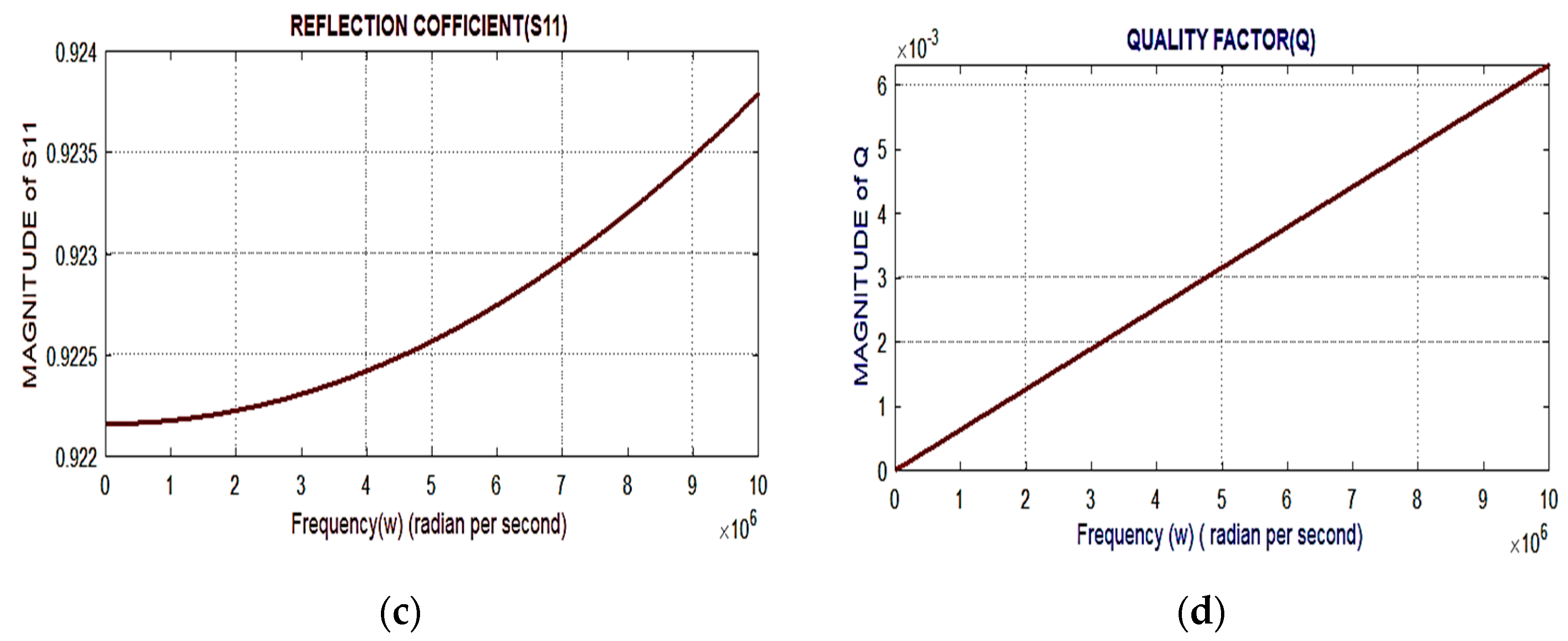
2.2.1. Quality Factor of Multi-Stacked DRA
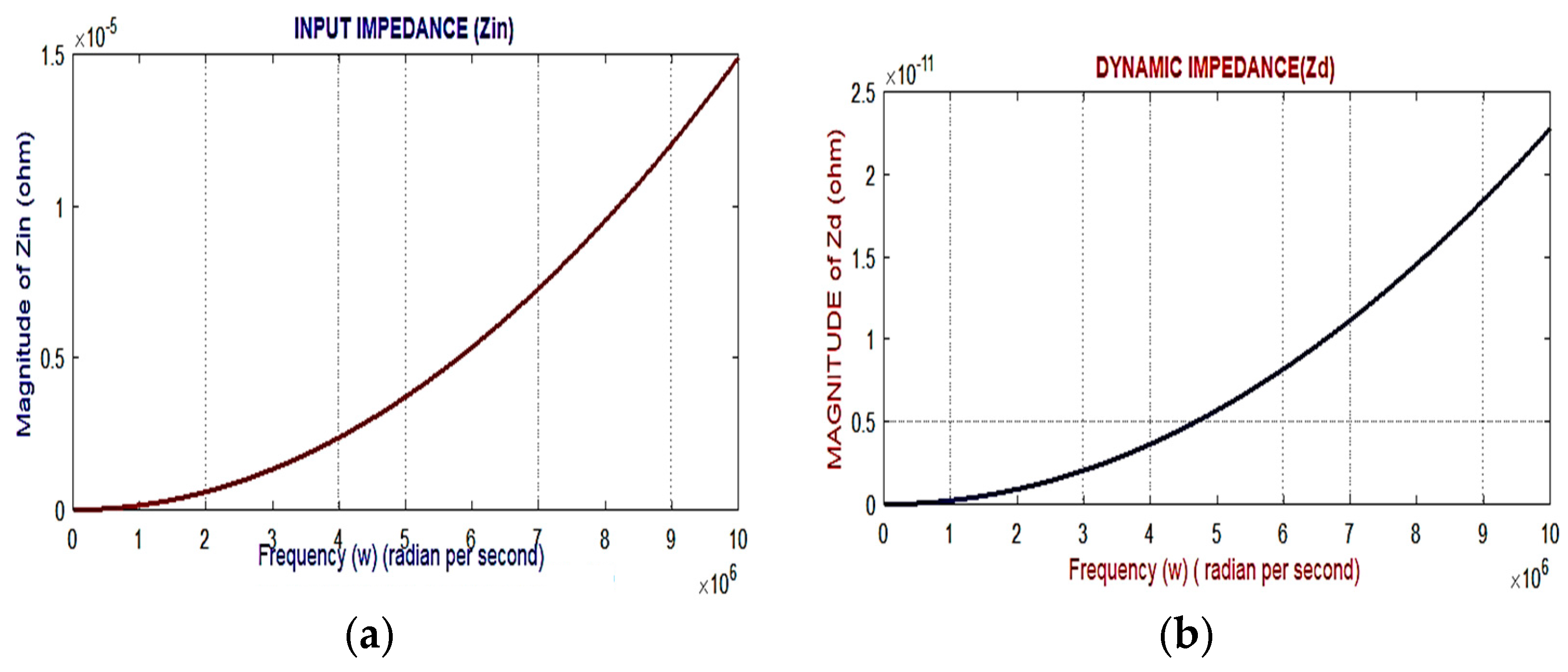
In MSDRA, the bandwidth will get reduced due to which the quality factor will be improved resulting in high selectivity and accuracy [24,25]. Therefore, the quality factor is given by the below equation:
Quality   factor   Q = resonance   frequency   Bandwidth = 1 2 n 2 L s + L E L n 2 L s + L E L n 2 L s c E L L E L + L E L L s c s
Input admittance Y i n = A + jB
Quality factor (Q) = B L A = B c A
Q ( ω ) = N 1 2 ω c s + N 1 2 N 2 2 P 2 + M 2 ω L c 1 + ω L c 2 + ω L c 3 + ω L c 4 + ω L c 5 + ω c d 1 + ω c d 2 + ω c d 3 + ω c d 4 + ω c d 5 + ω c d 6 N 1 2 R s + P N 1 2 N 2 2 P 2 + M 2 = N 1 2 R s + N 1 2 N 2 2 P 2 + M 2 i = 1 n p i
Q ω = N 1 2 ω c s + N 1 2 N 2 2 P 2 + M 2 i = 0 n 1 ω L C 3 + i = 0 n ω c d i N 1 2 R s + N 1 2 N 2 2 P 2 + M 2 i = 1 n p i
As the quality factor is dependent upon R, L and C it is observed that the quality factor increases with an increase in capacitance and with decreases in inductance of corresponding DRA units. Therefore, cascading will increase the quality factor [26].
Q d 1 = R d 1 C d 1 L d 1   f o r   D R A   1 ; Q d 2 = R d 2 C d 2 L d 2   f o r   D R A   2 ; Q d 3 = R d 3 C d 3 L d 3   f o r   D R A   3 , Q d 4 = R d 4 C d 4 L d 4   f o r   D R A   4 ; Q d 5 = R d 5 C d 5 L d 5   f o r   D R A   5 ; Q d 6 = R d 6 C d 6 L d 6   f o r   D R A   6 ; Q s = R s C s L s
For slot C d 6 > C d 5 > C d 4 > C d 3 > C d 2 > C d 1 > C s & L d 6 < L d 5 < L d 4 < L d 3 < L d 2 < L d 1 < L s
As the quality factor is increased, bandwidth will get decreased.
Bandwidth (BW) = 1 R s C s = 1 τ s for slot
Bandwidth (BW) = 1 R d 1 C d 1 = 1 τ d 1 for DRA-1
Bandwidth (BW) = 1 R d 2 C d 2 = 1 τ d 2 for DRA-2, similarly for DRA-6
The time constant of the circuit is τ d 6 > τ d 5 > τ d 4 > τ d 3 > τ d 2 > τ d 1 > τ s because the capacitance increases.
Quality   factor = Resonance   frequency Bandwidth
Bandwidth is decreased as the time constant is increased τ = RC.
In DRA, selectivity depends upon the quality factor and inversely depends on bandwidth. A higher-order mode will result in higher currents in DRA. The Quality factor (Q) depends on the permittivity of the material. Low Q will dissipate and high Q will store energy in DRA [27]. The input voltage of the DRA unit is the same as the input voltage of the slot except this voltage is scaled by the factor N 1 N 2 , due to the coupling transformer at the input of DRA. With the addition of more DRA units in parallel, the equivalent resistance and inductance concerning the source decrease, and the equivalent capacitance increases, because of that, the quality factor increases [28,29].

2.2.2. Dynamic Impedance ( Z d ) of Multi-Stacked DRA

The expression of Zd & Z i m g defines the dynamic impedance and imaginary part of the input impedance of multi-stacked DRA as given below [30].
Z d = 1 R d 1 1 R d 1 2 + ( ω c d 1 1 ω L d 1 ) 2 + + 1 R d 6 1 R d 6 2 + ( ω c d 6 1 ω L d 6 ) 2
Z i m g = ω L c 1 1 ω C c 1 + + ω L c 5 1 ω C c 5 ω c d 1 1 ω L d 1 1 R d 1 2 + ( ω c d 1 1 ω L d 1 ) 2 ω c d 6 1 ω L d 6 1 R d 6 2 + ( ω c d 6 1 ω L d 6 ) 2

2.2.3. Reflection Coefficient of Multi-Stacked DRA

The expression of the reflection coefficient is derived below for the multi-stacked DRA [31]:
Γ = Z L Z 0 Z L + Z 0   = S 11
Z 0 = R s + j ω L s 1 R s + j ω C s   = R s 2 + j ω L s R s 1 + j ω C s R s = R s 2 + j ω L s R s ( 1 j ω C s R s 1 + j ω C s R s ( 1 j ω C s R s = R s 2 + ω 2 L s R s 2 C s + j ω L s R s ω C s R s 3 1 + ω 2 C s R s
Z 0 = R s 2 + ω 2 L s R s 2 C s 1 + ω 2 C s R s 1 + j ω L s R s ω C s R s 3 2 R s 2 + ω 2 L s R s 2 C s = D + j F
where
Z 0   is   the   characteristic   impedance   of   the   slot
Real part of Z 0 (D) = R s 2 + ω 2 L s R s 2 C s 1 + ω 2 C s R s
Imaginary part of Z 0 (F) = ω L s R s ω C s R s 3 2 1 + ω 2 C s R s R s 2 + ω 2 L s R s 2 C s
Z L = Z d 1 + Z c 12 + Z d 2 + Z c 23 + Z d 3 + Z c 34 + Z d 4 = P + j X
where
P = i = 1 n p i ,   P = p 1 + p 2 + p 3 + p 4 + p 5 + + p n
p i = 1 R d i 1 R d i 2 + ( ω c d i 1 ω L d i ) 2 and X = H L
where L = i = 1 n l i , L = l 1 + l 2 + l 3 + l 4 + l 5 + + l n then
l i = ω c d i 1 ω L d i   1 R d i 2 + ( ω c d i 1 ω L d i ) 2   and   H = i = 1 n j = 2 m h i j ,   H = h 12 + h 23 + h 34 + + h n m
h i j = ω L i j 1 ω C i j
Γ = Z L Z 0 Z L + Z 0 =   S 11 =   P + j X D + j F P + j X + D + j F = P + D + j X F P + D + j X + F
The magnitude of the complex reflection coefficient
S 11 = Г = P + D + j X F P + D + j X + F Г = P D 2 + X F 2 P + D 2 + X + F 2

3. Implementation of Proposed Multi-Staked DRA (MSDRA)

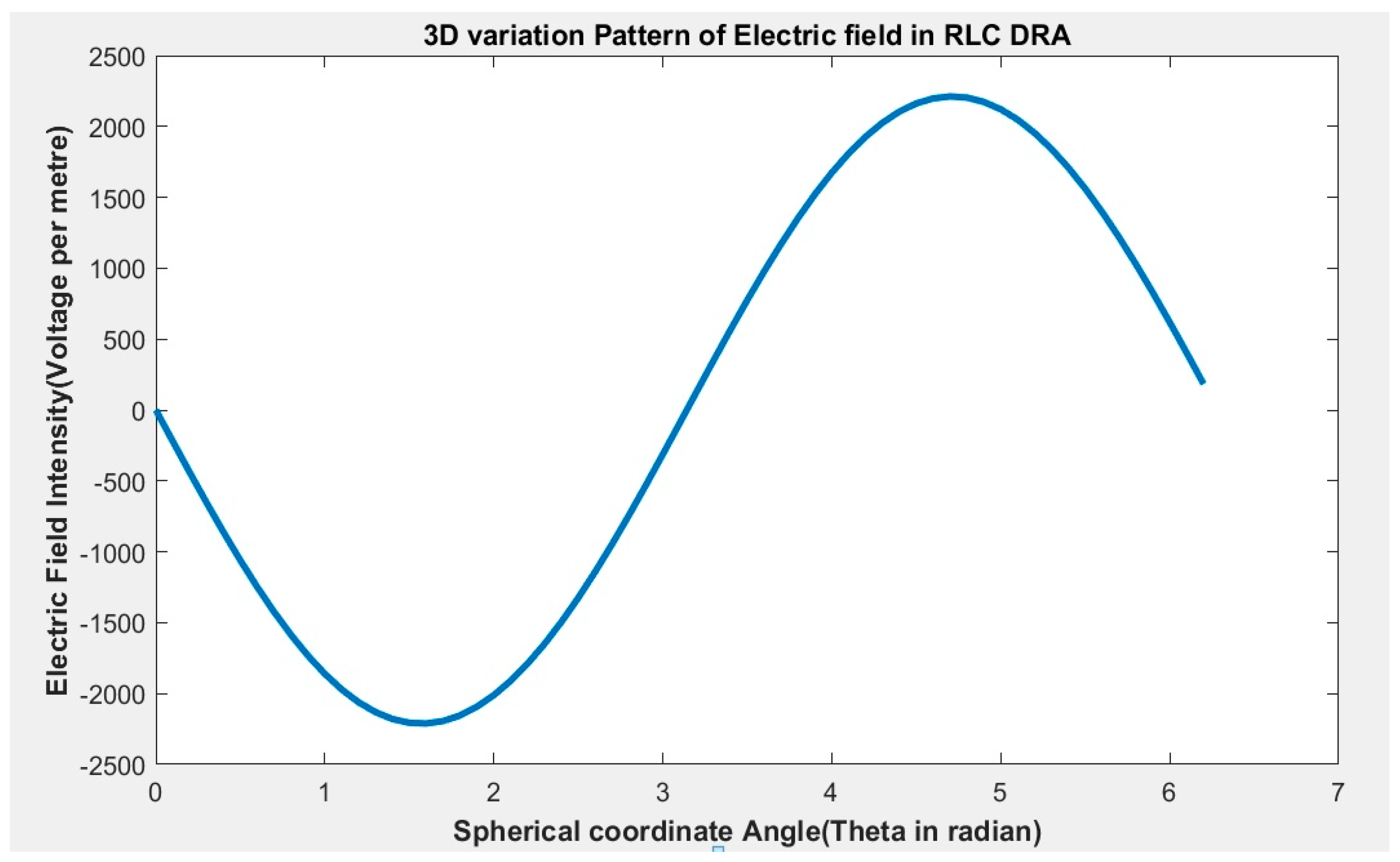
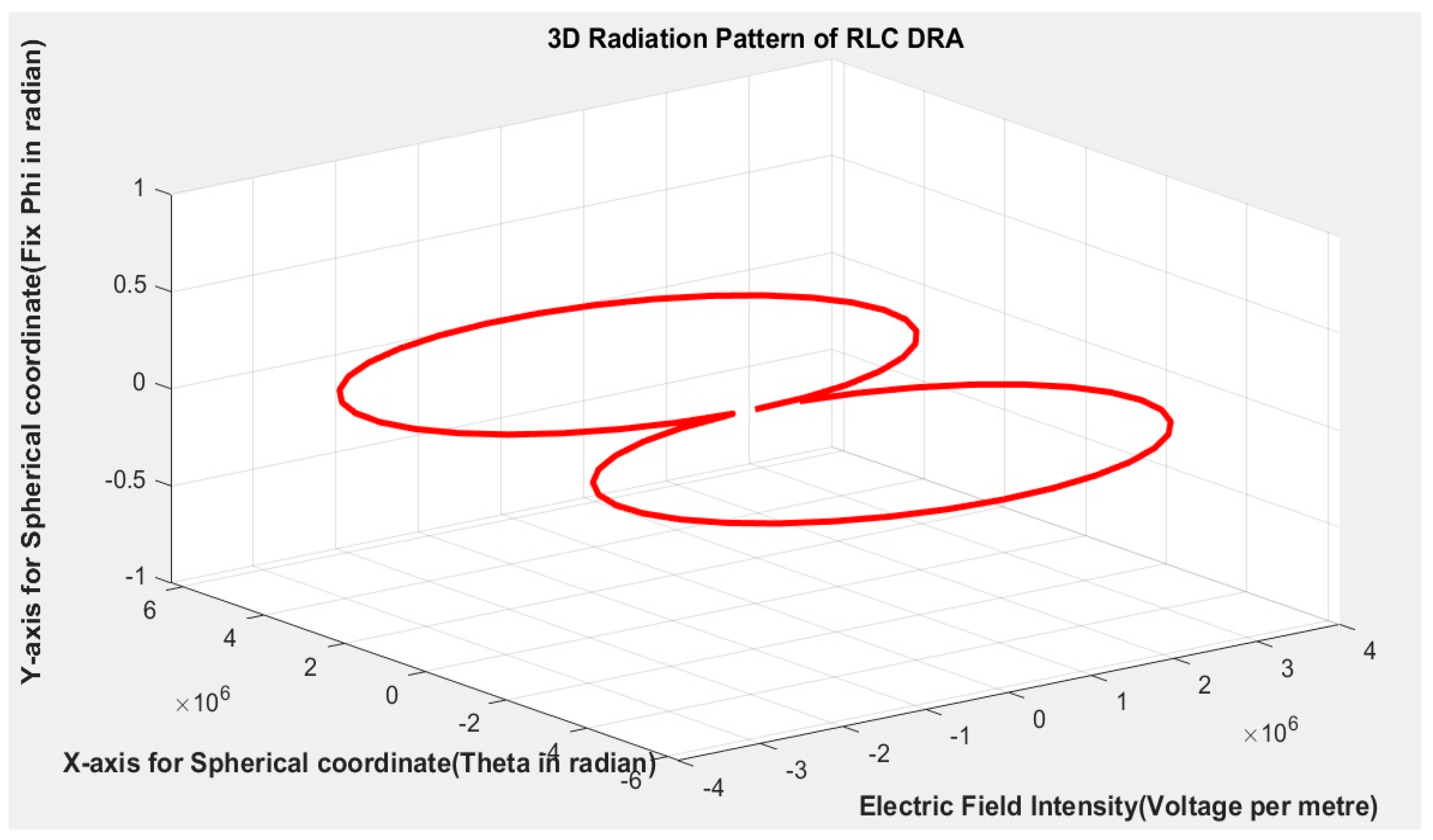
3.1. Simulation Results of Proposed Multi-Stacked DRA (MSDRA) Using MATLAB

Figure 4a–d below illustrate the results of simulation for input impedance, dynamic impedance, refraction coefficient, and quality factor of the suggested multi-stacked DRA.
It is observed from Figure 4a that the magnitude of the input impedance of MSDRA increases with the increase in frequency in the THz spectrum. Similarly, the dynamic impedance, reflection coefficient, and quality factor of MSDRA increase with the increase in frequency in the THz spectrum as shown in Figure 4b–d respectively.
The permittivity of the material used, cavity size of the multi-stacked DRA, reactance, resistance, and frequency of operation of the MSDRA all influence the quality factor of the MSDRA.

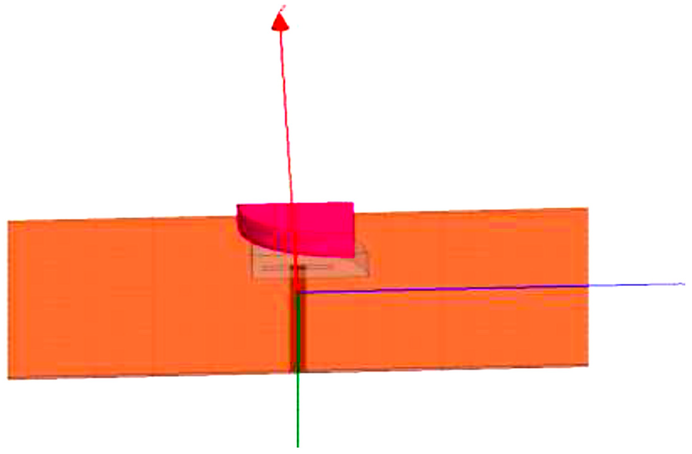
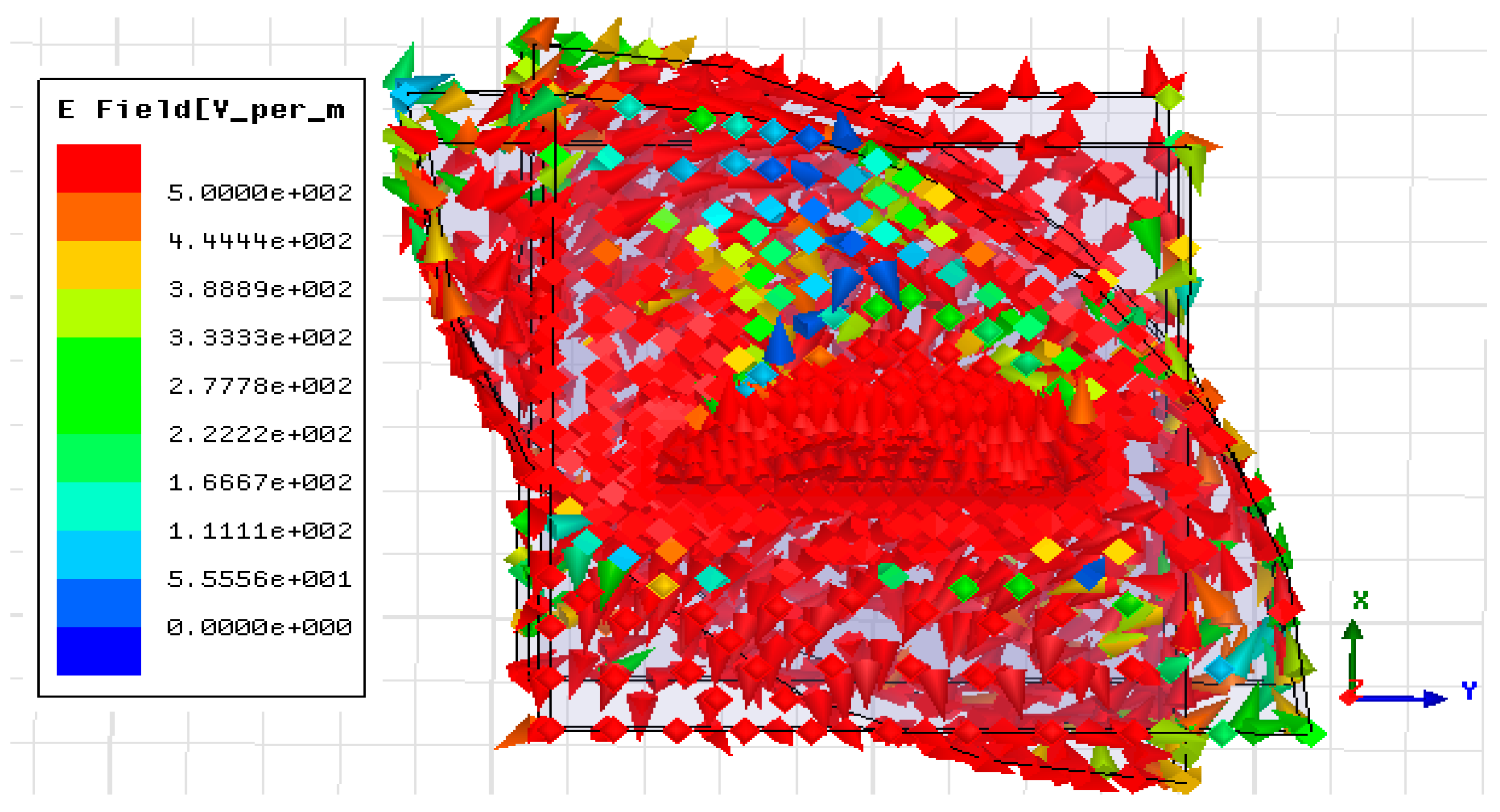
3.1.1. Hardware Design and Evaluation of a Multi-Stacked DRA Using HFSS

A 40 Giga Hertz vector network analyzer (VNA) was used to measure the reflection coefficient (S11) of multi-stacked DRA, as illustrated in Figure 5. Figure 6 shows the HFSS model as well. The resultant circuit of multi-stacked DRA has been shown in Figure 3 with an input impedance (Zin) solution. Figure 7 depicts an aperture-coupled multi-stacked DRA [32]. Table 1 shows the designing dimensions of multi-stacked DRA. Electric fields have been shown in Figure 8 and Figure 9.
Figure 7 and Table 2 show the hardware and tuning parameters for multi-stacked DRA for two stages. The simulation and validation results of the Multi-staked DRA(2-stage) with tuned parameters using HFSS software are quite good compared to existing ones.

3.1.2. Multi-Stacked DRA Radiation Theory

For any DRA, if the expression of magnetic vector potential is known then all the features of such type of DRA, are analyzed by evaluating electric and magnetic field properties. The mathematical calculation of magnetic vector potential is given below [33]:
  • Magnetic Vector Potential
A = L μ I d l 4 π r   where   I 0   = N 1 N 2 V m cos ω t Z L
I 0   = N 1 N 2 V m cos ω t R u Z L ,   I 0   = N 1 N 2 V m cos ω t ω R u Z L
I 0 =   N 1 N 2 V m cos ω t β r Z L ,   R = r r ,   I 0 = R e N 1 N 2 V m Z L e i ω t β r
A =   N 1 μ N 2 V m 4 π Z L L e i β r r d l , A φ =   N 1 μ N 2 V m S 4 π Z L r 2 1 + i β r sin θ e i β r s i = π R i 2
S = i = 1 n s i ,   A φ =   N 1 μ N 2 V m S 4 π Z L r 2 1 + i β r sin θ e i β r
This magnetic potential is time-varying and depends upon the space. Only φ component is present [34,35].
A φ =   N 1 μ N 2 V m S 4 π Z L r 2 1 + i β r sin θ e i β r and also calculated E and H field using the following formula; B =   X A , μ H =   X A ,   X H s = j ω ε E s
Another formula for the time-varying field is; E = V d A d t , E = d A d t , E φ s = d A φ s d t
E φ s = d d t N 1 μ N 2 V m S 4 π Z L r 2 1 + i β r sin θ e i β r = = N 1 μ N 2 V m S 4 π Z L r 2 sin θ d d t 1 + i β r e i β r
E φ s   = N 1 μ N 2 V m S 4 π Z L r 2 sin θ d d t cos ( ω t β r ) + j β r cos ω t β r
E φ s   = N 1 μ N 2 V m S 4 π Z L r 2 sin θ ω sin ( ω t β r ) j β r ω sin ω t β r
E φ s   = ω N 1 μ N 2 V m S 4 π Z L r 2 sin θ sin ( ω t β r ) + j β r sin ω t β r = j ω N 1 μ N 2 V m S 4 π Z L r 2 sin θ e i β r + j β r e i β r
E φ s = j ω N 1 μ N 2 V m S 4 π Z L sin θ j β r + 1 r 2 e i β r a ^ φ
where, Z L = Z d 1 + Z c 1 + Z d 2 + Z c 2 + Z d 3 + Z c 3 + Z d 4 + Z c 1 + Z d 5 + Z c 1 + Z d 6
H s is calculated using two methods [36].
B =   X A ,   μ H =   X A ,   X E s =   j ω μ H s
μ H =   X A = 1 h 1 h 2 h 3 h 1 a ^ u h 2 a ^ v h 3 a ^ w d d u d d v d d w h 1 A u h 1 A v h 1 A w
μ H =   X A = 1 r 2 sin θ a ^ r r a ^ θ r sin θ a ^ φ d d r d d θ d d φ A r r A θ r sin θ A φ
where A r and A θ is equal to zero.
μ H =   X A = 1 r 2 sin θ a ^ r r a ^ θ r sin θ a ^ φ d d r d d θ d d φ 0 0 r sin θ A φ
μ H =   X A = 1 r 2 sin θ d r sin θ A φ d θ a ^ r r d r sin θ A φ d r a ^ θ
μ H = N 1 μ N 2 V m S 4 π Z L sin θ e i β r 1 r 3 + j β r 2 β 2 r a ^ θ + N 1 μ N 2 V m S 4 π Z L cos θ 1 r 3 + j β r 2 e i β r a ^ r
H s = N 1 N 2 V m S 4 π Z L sin θ e i β r 1 r 3 + j β r 2 β 2 r a ^ θ + N 1 N 2 V m S 4 π Z L cos θ 1 r 3 + j β r 2 e i β r a ^ r
H s = H θ a ^ θ + H r a ^ r
H θ s = N 1 N 2 V m S 4 π Z L sin θ e i β r 1 r 3 + j β r 2 β 2 r a ^ θ ,   H r s = N 1 N 2 V m S 4 π Z L cos θ 1 r 3 + j β r 2 e i β r a ^ r
P s = E s ×   H s ,   P s = ( E φ a ^ φ ) × H θ a ^ θ + H r a ^ r
P s = E φ H θ a ^ r + E φ H r a ^ θ  
P s = j ω μ N 1 2 N 2 2 V m 2 S 2 16 π 2 Z L 2 sin θ cos θ j 2 β r 4 + 1 r 5 β 2 r 3 e 2 j β r a ^ θ + j ω μ N 1 2 N 2 2 V m 2 S 2 16 π 2 Z L 2 s i n 2 θ e 2 j β r a ^ r  
To calculate the resonant frequency of the proposed DRA’s following formulas are used [37]:
ϵ r = ϵ ϵ o   ;   f r m n p = c 2 π ϵ r ( m π a ) 2 + ( n π b ) 2 + ( p π 2 d ) 2
The DRA formulations’ length, the width of the slot, and the Stub dimension are given as [38]:
L S   = 0.4 λ o ε e ; W s = 0.2 L s ; L s t u b = λ g 4 ,   λ 2 π < r < 2 D 2 λ   ; for near far field, k >> >1; and
For far distance field as r > 2 D 2 λ ;
Where λ o = Wavelength and Effective permittivity; ε effective = ε r + ε s 2
Where ε r   and   ε s are the dielectric constant of the rectangular dielectric resonator and substrate, respectively.
λ g = λ 0 ε e f f , where λ 0 , λ g are the wavelengths of free space and guided medium
In general, a perfect electric conductor (PEC) and a perfect magnetic conductor (PMC) are used to determining the boundary condition [39,40,41].
For PEC walls; n × E = 0, and n. H = 0 and for PMC walls; n × H = 0, and n. E = 0.
ϵ r k 0 2 = k x 2 + k y 2 + k z 2 ; characteristic equation.
k x = m π / a , k y = n π / b , k z = p π / d
Where dimensions are; a, b, and d and indices; m, n, and p, respectively.
k = 2 π / λ = ω μ ϵ 2 = ω / c ;
k z tan k z d 2 = r 1 k 0 2 k z 2 ;   transcendental   equation
E 2   d V = H 2   d V
  • Boundary Conditions of Electric Wally (PEC)
n × E = 0 and n . H = 0
At z = 0, d the DRA is an interface and the normal component of the magnetic field and the tangential component of the electric field are both equal to “zero”.
Boundary Conditions of the Magnetic Wall (PMC)
n × H = 0   and   n . E = 0
E x = 1 j ω ε 1 + γ 2 k 2 H z y 1 j ω μ 2 E z z x
E y = 1 j ω ε 1 + γ 2 k 2 1 j ω μ 2 E z z y H z x
H x = 1 j ω μ 1 + γ 2 k 2 E z y 1 j ω ε 2 H z z x
H y = 1 j ω μ 1 + γ 2 k 2 1 j ω ε 2 H z z y E z x
  • TE Mode ( E z = 0   a n d   H z 0 )
H z = B sin m π a x sin n π b y   sin ( k z z )
Similarly, Ez fields can be calculated for TM mode.

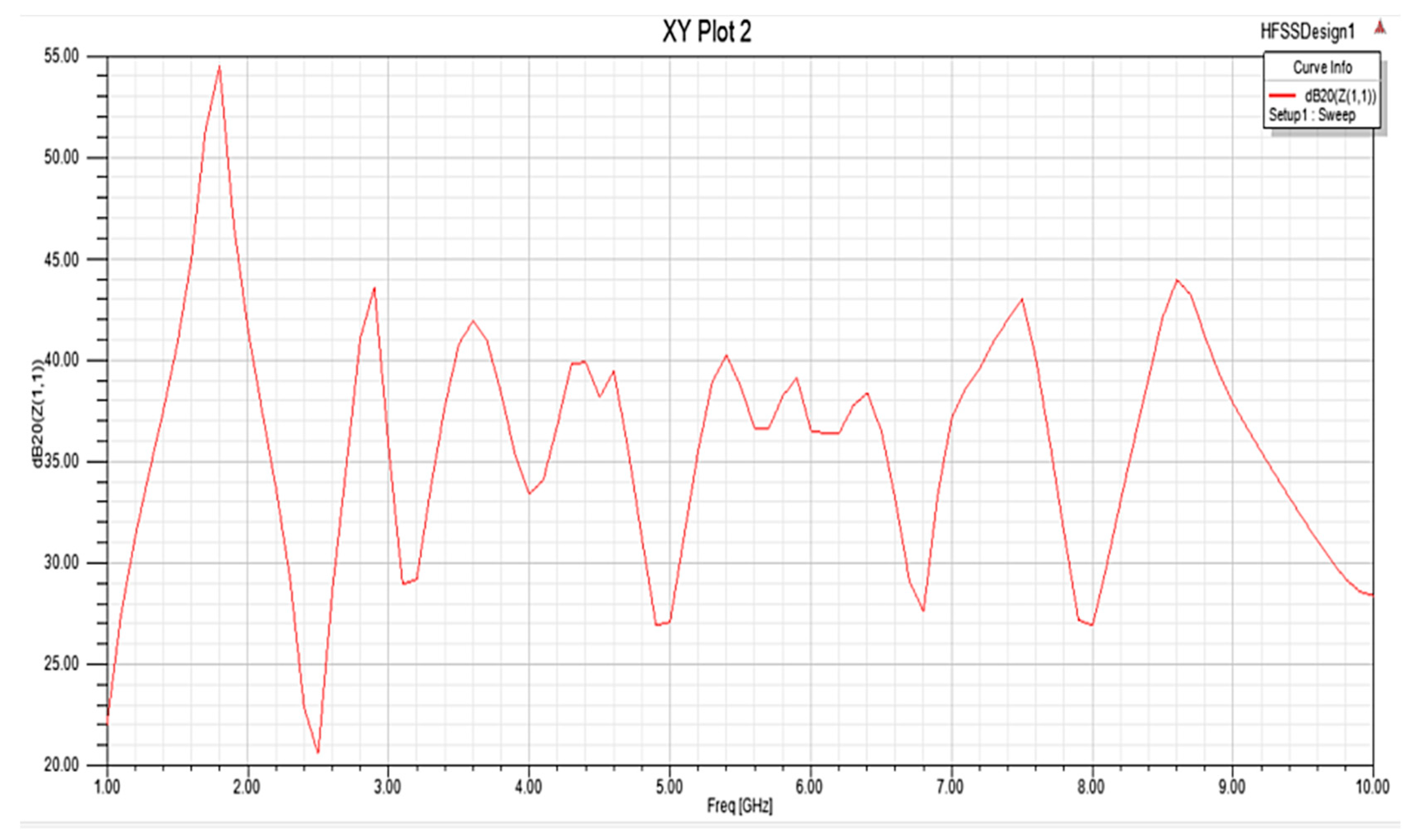
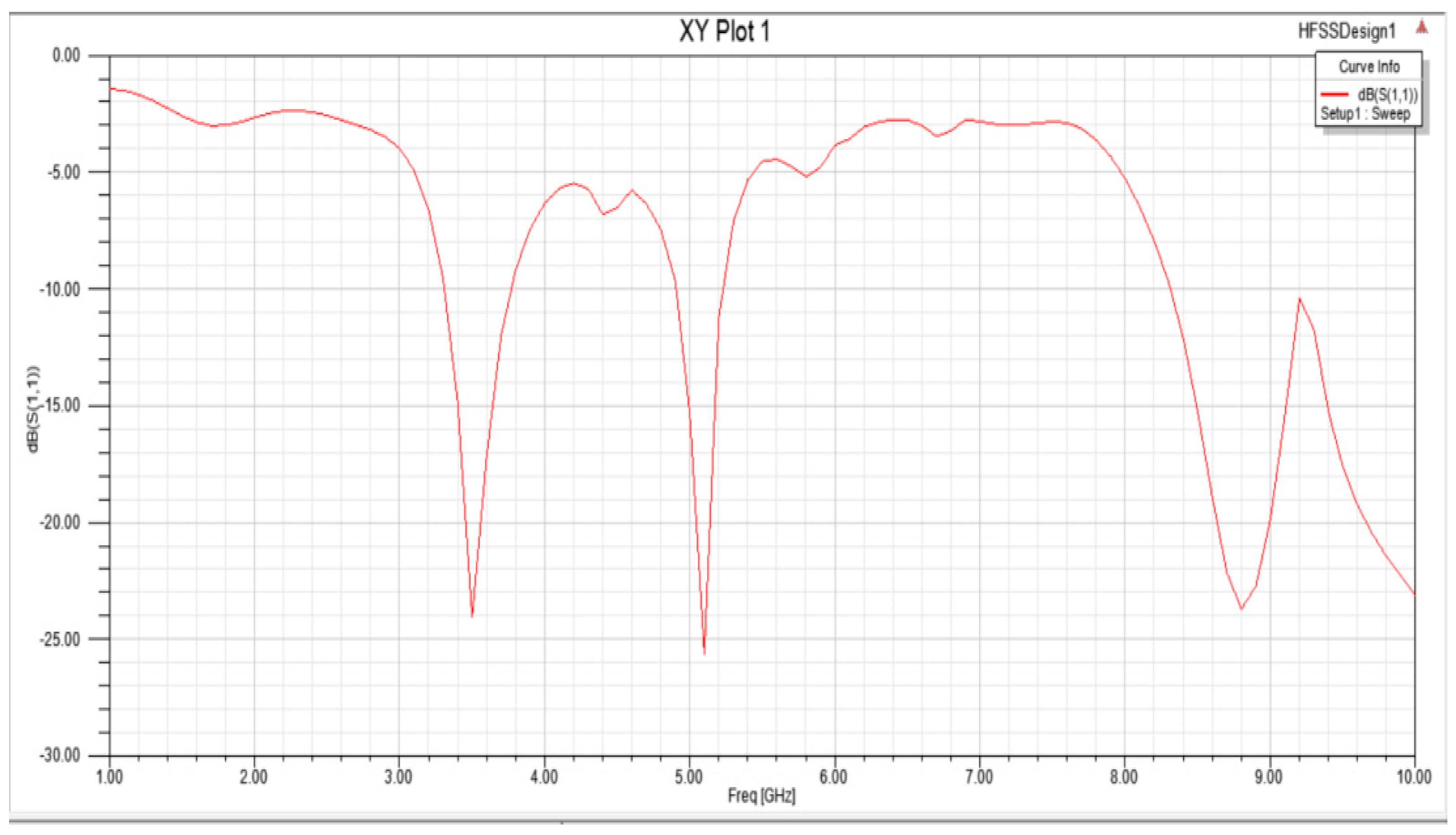
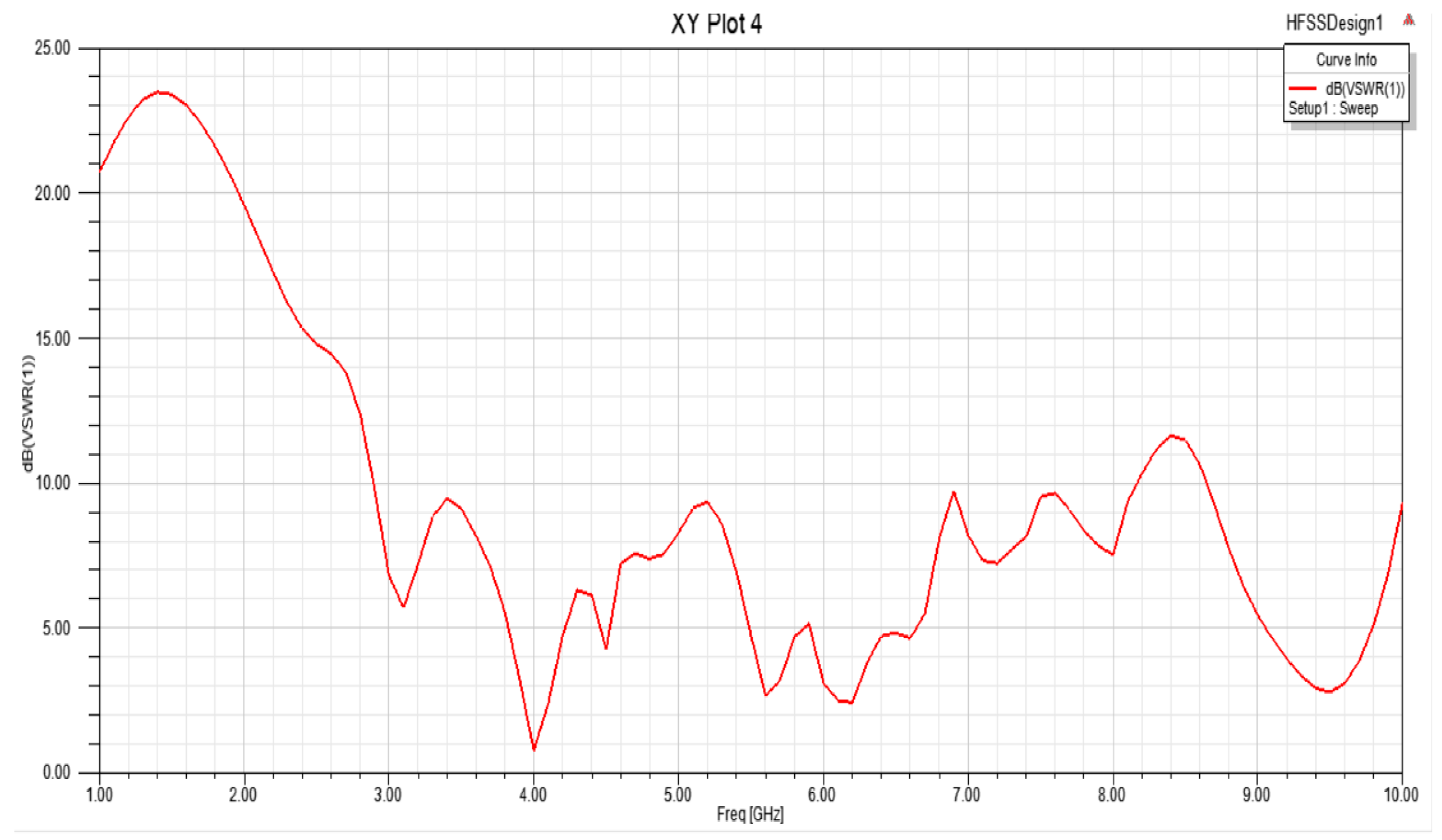
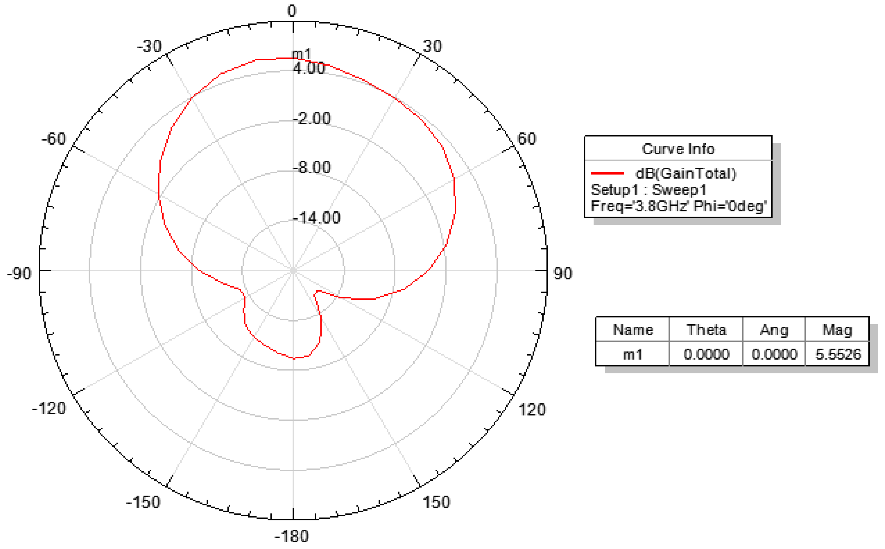
3.2. Simulation and Corresponding Parameters of Proposed MSDRA Using HFSS

The simulations and corresponding parameters of the proposed MSDRA using HFSS are presented in this section.
Figure 10 and Figure 11 show the electric field pattern obtained via HFSS in multi-stacked DRA for two different values of phase angles. Figure 12 shows the variation of input impedance (Impedance spectrum) of MSDRA with frequency. Figure 13 shows the variation of the reflection coefficient of MSDRA with frequency. Figure 14 shows the variation of the voltage standing wave ratio of MSDRA with frequency. Figure 15 shows the radiation pattern of MSDRA at 3.8 GHz frequency and 0 degrees . It has been observed that the quality factor is improved, bandwidth is reduced and selectivity is improved by implementing multi-stacked DRA over the basic DRA. This leads to an increase in the catching power of DRA, which results in higher performance from an application point of view.

4. Conclusions

The rectangular shape multi-stacked DRA has better flexibility, and it required moderate gain as compared to cylindrical DRA for selecting a resonant frequency due to its three degrees of freedom. The bandwidth and quality factor of single-stage DRA is fixed and depends on the value of R, L, and C components. To improve the quality factor and selectivity of DRA, a high value of R, L, and C components are required and it becomes bulky. Therefore, a rectangular-shaped multi-stacked DRA using parallel R, L, and C with L and C component coupling is proposed. The storing power of the antenna is increased due to an increase in capacitance. The quality factor and selectivity are also improved because it directly depends on stored energy with an optimal size of the antenna. The coefficient of reflection, radiation pattern, dynamic impedance, and input impedance of multi-stacked DRA has been estimated using the RLC circuit as an equivalent circuit of multi-stacked DRA. The calculated and simulated outcomes of multi-stacked DRA are presented. The analysis of the equivalent circuit configuration has been accomplished for the first time in this study. The equivalent circuit is utilized to develop the theoretical model that would help wireless network designers to recognize multi-stacked DRA circuits for specific applications. Summarily, the quality factor and selectivity are improved by a factor of 10%, and bandwidth decreased by implementing the proposed multi-stacked DRA. Future work would investigate the design and development of cost-efficient and optimal multi-stacked DRA systems for application in 5G and beyond 5G wireless communication systems.

Author Contributions

The manuscript was written through the contributions of all authors. Conceptualization, R.K. and R.S.Y.; methodology, R.S.Y., and H.S.; software, A.K.R., R.K. and R.S.Y.; validation, A.L.I., A.K.R., R.K. and R.S.Y.; formal analysis, A.L.I.; investigation, S.K.P.; resources, R.S.Y.; data curation, R.K.; writing—original draft preparation, A.L.I., A.K.R., R.K. and R.S.Y.; writing—review and editing, A.K.R., R.K., R.S.Y. and A.L.I.; visualization, R.K, H.S. and R.S.Y.; supervision, S.K.P.; project administration, S.K.P. and A.L.I.; funding acquisition, A.L.I. All authors have read and agreed to the published version of the manuscript.

Funding

The work of Agbotiname Lucky Imoize is supported in part by the Nigerian Petroleum Technology Development Fund (PTDF) and in part by the German Academic Exchange Service (DAAD) through the Nigerian-German Postgraduate Program under grant 57473408.

Data Availability Statement

The data that supports the findings of this paper is available upon reasonable request from the corresponding author.

Conflicts of Interest

The authors declare no conflict of interest.

References

  1. Ansarizadeh, M.; Ghorbani, A.; Abd-Alhameed, R.A. An approach to equivalent circuit modeling of rectangular microstrip antennas. Prog. Electromagn. Res. 2008, 8, 77–86. [Google Scholar] [CrossRef] [Green Version]
  2. Van Schelven, R.M.; Cavallo, D.; Neto, A. Equivalent circuit models of finite slot antennas. IEEE Trans. Antennas Propag. 2019, 67, 4367–4376. [Google Scholar] [CrossRef] [Green Version]
  3. Sun, S.; Rappaport, T.S.; Shafi, M.; Tang, P.; Zhang, J.; Smith, P.J. Propagation models and performance evaluation for 5G millimeter-wave bands. IEEE Trans. Veh. Technol. 2018, 67, 8422–8439. [Google Scholar] [CrossRef]
  4. Medbo, J.; Kyosti, P.; Kusume, K.; Raschkowski, L.; Haneda, K.; Jamsa, T.; Nurmela, V.; Roivainen, A.; Meinila, J. Radio propagation modeling for 5G mobile and wireless communications. IEEE Commun. Mag. 2016, 4, 144–151. [Google Scholar] [CrossRef]
  5. Hur, S.; Kim, T.; Love, D.J.; Krogmeier, J.V.; Thomas, T.A.; Ghosh, A. Millimeter wave beamforming for wireless backhaul and access in small cell networks. IEEE Trans. Commun. 2013, 61, 4391–4403. [Google Scholar] [CrossRef] [Green Version]
  6. Zebiri, C.E.; Lashab, M.; Sayad, D.; Elfergani, I.T.E.; Sayidmarie, K.H.; Benabdelaziz, F.; Abd-Alhameed, R.A.; Rodriguez, J.; Noras, J.M. Offset aperture-coupled double-cylinder dielectric resonator antenna with extended wideband. IEEE Trans. Antennas Propag. 2017, 65, 5617–5622. [Google Scholar] [CrossRef] [Green Version]
  7. Yaduvanshi, R.S.; Parthasarathy, H. Rectangular Dielectric Resonator Antennas; Springer: New Delhi, India, 2016; pp. 1–365. [Google Scholar]
  8. Varshney, G.; Pandey, V.S.; Yaduvanshi, R.S.; Kumar, L. Wideband circularly polarized dielectric resonator antenna with stair-shaped slot excitation. IEEE Trans. Antennas Propag. 2016, 65, 1380–1383. [Google Scholar] [CrossRef]
  9. Oleiwi, H.W.; Saeed, N.; Al-Raweshidy, H. Cooperative SWIPT-Hybrid-NOMA pairing scheme considering SIC im-perfection for THz communications. In Proceedings of the IEEE 4th Global Power, Energy and Communication Conference (GPECOM), Cappadocia, Turkey, 14–17 June 2022; pp. 638–643. [Google Scholar]
  10. Kremer, H.I.; Leung, K.W.; Wong, W.C.; Lo, K.K.W.; Lee, M.W.K. Design of Dielectric Resonator Antenna Using Dielectric Paste. Sensors 2021, 21, 4058. [Google Scholar] [CrossRef]
  11. Chauhan, M.; Mukherjee, B. Wideband circular polarized cylindrical segmented dielectric resonator antenna for ISM band applications. Int. J. RF Microw. Comput. Aided Eng. 2020, 30, e22134. [Google Scholar] [CrossRef]
  12. Oleiwi, H.W.; Saeed, N.; Al-Raweshidy, H. SWIPT-Pairing mechanism for channel-aware cooperative H-NOMA in 6G Terahertz communications. Sensors 2022, 22, 6200. [Google Scholar] [CrossRef]
  13. Gupta, S.; Kshirsagar, P.; Mukherjee, B. A Low-Profile Multilayer Cylindrical Segment Fractal Dielectric Resonator Antenna: Usage for wideband applications. IEEE Antennas Propag. Mag. 2019, 61, 55–63. [Google Scholar] [CrossRef]
  14. Wang, F.; Zhang, C.; Sun, H.; Xiao, Y. Ultra-Wideband Dielectric Resonator Antenna Design Based on Multilayer Form. Int. J. Antennas Propag. 2019, 43, 1–11. [Google Scholar] [CrossRef]
  15. Chauhan, M.; Mukherjee, B. High Gain Fractal Cylindrical Dielectric Resonator Antenna for UWB Application. In Proceedings of the 2018 IEEE Radio and Antenna Days of the Indian Ocean (RADIO), Wolmar, Mauritius, 15–18 October 2018; pp. 1–2. [Google Scholar]
  16. Singh, M.; Yaduvanshi, R.S.; Vaish, A. Design for enhancing gain in multimodal cylindrical dielectric resonator antenna. In Proceedings of the 2015 Annual IEEE India Conference (INDICON), New Delhi, India, 17–20 December 2015; pp. 1–4. [Google Scholar]
  17. Gotra, S.; Varshney, G.; Yaduvanshi, R.S.; Pandey, V.S. Dual-band circular polarization generation technique with the miniaturization of a rectangular dielectric resonator antenna. IET Microw. Antennas Propag. 2019, 13, 1742–1748. [Google Scholar] [CrossRef]
  18. Singh, M.; Gautam, A.K.; Yaduvanshi, R.S.; Vaish, A. An investigation of resonant modes in rectangular dielectric resonator antenna using transcendental equation. Wirel. Pers. Commun. 2017, 95, 2549–2559. [Google Scholar] [CrossRef]
  19. Bakshi, G.; Vaish, A.; Yaduvanshi, R.S. Two-Layer sapphire rectangular dielectric resonator antenna for rugged communications. Prog. Electromagn. Res. 2019, 85, 73–80. [Google Scholar] [CrossRef] [Green Version]
  20. Kumar, G.; Singh, M.; Ahlawat, S.; Yaduvanshi, R.S. Design of stacked rectangular dielectric resonator antenna for wideband applications. Wirel. Pers. Commun. 2019, 97, 1661–1672. [Google Scholar] [CrossRef]
  21. Khan, R.; Jamaluddin, M.H.; Kazim, J.U.R.; Nasir, J.; Owais, O. Multiband-dielectric resonator antenna for LTE application. IET Microw. Antennas Propag. 2016, 10, 595–598. [Google Scholar] [CrossRef]
  22. Ambrosio, L.A.; Hernández-Figueroa, H.E. RLC circuit model for the scattering of light by small negative refractive index spheres. IEEE Trans. Nanotechnol. 2012, 11, 1217–1222. [Google Scholar] [CrossRef]
  23. Tzarouchis, D.P.; Ylä-Oijala, Y.; Sihvola, A. Resonant scattering characteristics of homogeneous dielectric sphere. IEEE Trans. Antennas Propag. 2017, 65, 3184–3191. [Google Scholar] [CrossRef] [Green Version]
  24. Mongia, R.K.; Bhartia, P. Dielectric resonator antennas—Are view and general design relations for resonant frequency and bandwidth. Int. J. Microw. Millim. Wave Comput. Aided Eng. 1994, 4, 230–247. [Google Scholar] [CrossRef]
  25. Guo, Y.; Zhang, T.; Yin, W.Y.; Wang, X.H. Improved hybrid FDTD method for studying tunable graphene frequency-selective surfaces (GFSS) for THz-wave applications. IEEE Trans. THz Sci. Technol. 2015, 5, 358–367. [Google Scholar] [CrossRef]
  26. Cao, Y.S.; Jiang, L.J.; Ruehli, A.E. An equivalent circuit model for graphene-based terahertz antenna using the PEEC method. IEEE Trans. Antennas Propag. 2016, 64, 1385–1393. [Google Scholar] [CrossRef]
  27. Christensen, T.; Jauho, A.P.; Wubs, M.; Mortensen, N.A. Localized plasmons in graphene-coated nanospheres. Phys. Rev. B 2015, 91, 125414. [Google Scholar] [CrossRef] [Green Version]
  28. Zou, L.; Withayachumnankul, W.; Shah, C.; Mitchell, A.; Bhaskaran, M.; Sriram, S.; Fumeaux, C. Dielectric resonator nano antennas at visible frequencies. Opt. Express 2013, 21, 1344–1352. [Google Scholar] [CrossRef] [PubMed] [Green Version]
  29. Malheiros-Silveira, G.N.; Wiederhecker, G.S.; Hernández-Figueroa, H.E. Dielectric resonator antenna for applications in nano photonics. Opt. Express 2013, 21, 1234–1239. [Google Scholar] [CrossRef]
  30. Mühlschlegel, P.; Eisler, H.; Martin, O.J.F.; Hecht, B.; Pohl, D.W. Resonant Optical Antennas. Science 2005, 308, 1607–1609. [Google Scholar] [CrossRef] [Green Version]
  31. Yaduvanshi, R.S.; Parthasarathy, H. Coupled Solution of Boltzmann Transport Equation, Maxwell’s and Navier Stokes equations. IJACSA 2010, 19, 114–124. [Google Scholar] [CrossRef]
  32. Zou, L.; Withayachumnankul, W.; Shah, C.; Mitchell, A.; Klemm, M.; Bhaskaran, M.; Sriram, S.; Fumeaux, C. Efficiency and scalability of dielectric resonator antennas at optical frequencies. IEEE Photon. J. 2014, 6, 4600110. [Google Scholar]
  33. Watts, C.M.; Liu, X.; Padilla, W.J. Metamaterial electromagnetic wave absorbers. Adv. Mater. 2012, 24, OP98–OP120. [Google Scholar] [CrossRef]
  34. Yadav, R.; Katiyar, S.; Yaduvanshi, R.S.; Nishtha, N.; Hecht, B. Principles of Nano-Optics. J. Inf. Optim. Sci. 2020, 41, 1375–1393. [Google Scholar]
  35. Fakhte, S.; Oraizi, H.; Matekovits, L. Gain improvement of rectangular dielectric resonator antenna by engraving grooves on its side walls. Antennas Wirel. Propag. Lett. 2017, 16, 2167–2170. [Google Scholar] [CrossRef]
  36. Altaf, A.; Seo, M. Dual-Band Circularly Polarized Dielectric Resonator Antenna for WLAN and WiMAX Applications. Sensors 2020, 20, 1137. [Google Scholar] [CrossRef]
  37. Liu, H.; Liu, Y.; Wei, M.; Gong, S. Dual-broadband dielectric resonator antenna based on modified sierpinski fractal geometry. Electron. Lett. 2015, 51, 806–808. [Google Scholar] [CrossRef]
  38. Awais, Q.; Jin, Y.; Chattha, H.T.; Jamil, M.; Qiang, H.; Khawaja, B.A. A compact rectenna system with high conversion efficiency for wireless energy harvesting. IEEE Access 2018, 6, 35857–35866. [Google Scholar] [CrossRef]
  39. Guo, L.; Li, X.; Sun, W.; Yang, W.; Zhao, Y.; Wu, K. Designing and modeling of a dual-band rectenna with compact dielectric resonator antenna. IEEE Antennas Wirel. Propag. Lett. 2022, 21, 1046–1050. [Google Scholar] [CrossRef]
  40. Shi, Y.; Fan, Y.; Li, Y.; Yang, L.; Wang, M. An efficient broadband slotted rectenna for wireless power transfer at LTE band. IEEE Trans. Antennas Propag. 2019, 67, 814–822. [Google Scholar] [CrossRef]
  41. Khan, K.; Mehmood, A.; Khan, S.; Khan, M.A.; Iqbal, Z.; Mashwani, W.K. A survey on intrusion detection and prevention in wireless ad-hoc networks. J. Syst. Archit. 2020, 105, 101701. [Google Scholar] [CrossRef]
Figure 1. Multi-stacked DRA equivalent circuit.
Mca 28 00004 g001
Figure 2. Multi-stacked DRA simplified circuit.
Mca 28 00004 g002
Figure 3. Equivalent multi-stacked DRA simplified circuit.
Mca 28 00004 g003
Figure 4. (a) Input impedance, (b) dynamic impedance, (c) reflection coefficient, and (d) quality factor of multi-stacked DRA.
Mca 28 00004 g004aMca 28 00004 g004b
Figure 5. The hardware of the 3.5 GHz aperture coupled MSDRA, measurements with a VNA.
Mca 28 00004 g005
Figure 6. The proposed aperture coupled MSDRA hardware at 3.5 Giga-Hertz.
Mca 28 00004 g006
Figure 7. The hardware of 3.5 GHz aperture coupled MSDRA.
Mca 28 00004 g007
Figure 8. The R-L-C DRA’s electric field configuration.
Mca 28 00004 g008
Figure 9. The Electric field configuration in the spherical coordinate of the proposed R-L-C DRA.
Mca 28 00004 g009
Figure 10. The pattern of electric fields inside a multi-stacked DRA.
Mca 28 00004 g010
Figure 11. Electric- field’s pattern inside multi-stacked DRA.
Mca 28 00004 g011
Figure 12. Impedance spectrum of multi-stacked DRA.
Mca 28 00004 g012
Figure 13. S11 plot of multi-stacked DRA.
Mca 28 00004 g013
Figure 14. VSWR of multi-stacked DRA.
Mca 28 00004 g014
Figure 15. The Radiation pattern of Multi-stacked DRA (MSDRA).
Mca 28 00004 g015
Table 1. Parameter information of proposed multi-stacked DRA.
Name of ParameterDimensions (Millimeters)
Length of Microstrip line64
Width of Microstrip line31
Ground Plane111 × 101
Substrate Height1.5
Length of Slot14
Width of Slot3
Length of Stub 24
Width of Stub14
Size of DRA (slab-wise size)21 × 21 × 8
Table 2. Used symbols in mathematical modeling with their Nomenclature.
SymbolNomenclature
i 0 (t)Current through shunt R-L-C circuit
f r Resonant frequency in Hz
ZdDynamic impedance
ZinInput impedance
QQuality factor
BWBandwidth
Y d 1 ,   Y d 2 ,   Y d 3 ,   Y d 4 ,   Y d 5 ,   Y d 6 Individual admittance of each DRA
R d 1 ,   R d 2 ,   R d 3 ,   R d 4 ,   R d 5 ,   R d 6 Individual Resistance of each DRA
Z C 1 ,   Z C 2 ,   Z C 3 ,   Z C 4 ,   Z C 5 ,   Z C 6 Individual coupling impedance between DRAs
s c d 1 ,   s c d 2 ,   s c d 3 ,   s c d 4 ,   s c d 5 ,   s c d 6 Laplacian capacitance of each DRA
s L d 1 ,   s L d 2 ,   s L d 3 ,   s L d 4 ,   s L d 5 ,   s L d 6 Laplacian Inductance of each DRA
s L C 1 ,   s L C 2 ,   s L C 3 ,   s L C 4 ,   s L C 5 ,Laplacian inductance & coupling of capacitance of each DRA
Z L   and   Z i n DRA load and input impedance
Ys and Y i n Slot and input admittance
N1 and N2Number of terns in the primary winding
A & BReal and imaginary part of input admittance Y i n
HEquivalent transformer coupler reactance of all stacked DRA
LEquivalent reactance of all stacked DRA
P & MReal and Imaginary part of Input Impedance
I o Current through the load impedance
I i n Current through source
W r Resonant frequency in radian per sec.
W 1 & W 2 Higher and lower resonant frequency in radians per sec.
Δ ω Bandwidth
LsSlot inductance
R E L Equivalent resistance of all stacked DRA
C E L Equivalent capacitance of each DRA with coupling capacitor between stacked DRA.
L E L Equivalent inductance of each DRA with coupling inductor between stacked DRA.
S 11 Magnitude of the complex reflection coefficient
E φ s Time-varying field
λ 0 , λ g Wavelength of free space and guided medium
ε r and ε s Dielectric constant of the rectangular DRA and substrate
Disclaimer/Publisher’s Note: The statements, opinions and data contained in all publications are solely those of the individual author(s) and contributor(s) and not of MDPI and/or the editor(s). MDPI and/or the editor(s) disclaim responsibility for any injury to people or property resulting from any ideas, methods, instructions or products referred to in the content.

