
Anisotropic Analysis of Etch Rates for Sapphire Based on a Layer-by-Layer Removal Model of Surface Atoms

School of Mechatronic Engineering, Taizhou University, Taizhou 225300, China
*
Author to whom correspondence should be addressed.
Processes 2023, 11(4), 1290; https://doi.org/10.3390/pr11041290
Submission received: 11 March 2023
/
Revised: 13 April 2023
/
Accepted: 20 April 2023
/
Published: 21 April 2023
(This article belongs to the Section Materials Processes)
Abstract
:In this paper, a layer-by-layer removal model of surface atoms (Al) is established according to the atomic structure of sapphire, which can accurately calculate etch rates of crystal planes and analyze the anisotropy of etch rates of sapphire. Firstly, etch rate distributions of sapphire are gained through different etching experiments of sapphire hemispheres, and the effect of concentrations of the etching solution on etch rate distributions are analyzed. Then, different types of surface atoms are classified based on the types of chemical bonds of surface atoms, the arrangement laws of surface atoms of different crystal planes are analyzed and a general formula for calculating etch rates of different planes is proposed. Finally, the effectiveness of the layer-by-layer removal model of surface atoms (Al) is proved by small errors between calculated rates of the model and experimental rates at different concentrations, and the factors affecting the anisotropy of etch rates of sapphire are summarized, which include: (1) the vertical distances between two adjacent layers of surface atoms of crystal planes; (2) the configurations of the types of surface atoms of crystal planes.
1. Introduction
Sapphire is widely used in MEMS due to its excellent light transmission [1,2], insulation [3,4,5] and chemical stability [6,7,8]. In particular, the patterned sapphire substrate processed by wet etching can effectively enhance luminescent properties of LED devices [9,10,11,12,13,14,15]. Sapphire is a typical trigonal system material with a complicated atomic structure, and its etching characteristics are characterized by complex anisotropy, which hinders the development of wet etching technology [16,17,18,19,20]. The anisotropic analysis of etch rates for sapphire is beneficial for improving the wet etching process of sapphire and establishing the corresponding simulation models [21,22,23,24].
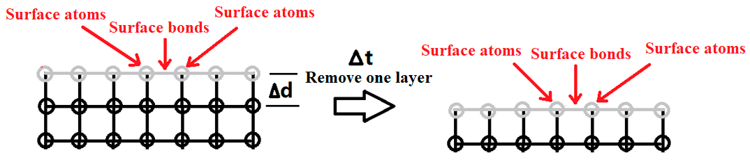
The different surface atomic arrangements of crystal planes are the main reasons affecting the anisotropy of etch rates of crystal planes [25,26,27,28]. Based on the microscopic atomic level, the wet etching of the crystal plane can be regarded as the process in which the atoms on its surface are gradually etched away. Due to its simple atomic structure, the anisotropic analysis of etch rates for silicon has been reported. In the wet etching of silicon, Zubel proposed the layer-by-layer removal model of surface atoms [29]. The model defines etching processes of different crystal planes as layer-by-layer removal processes of surface atoms, so the etch rate of the crystal plane is equivalent to the ratio of the vertical distance between adjacent two layers of surface atoms to the removal time of one layer of surface atoms, as shown in Figure 1.
For each crystal plane, the vertical distance between adjacent two layers of surface atoms is determined by the atomic structure of the crystal planes itself, which can be calculated by the trigonometric function of the geometric parameters of the atomic structure of sapphire. The time required to remove a layer of surface atoms is the key to calculate the etch rate of each crystal plane. The model classifies types of surface atoms according to their surface chemical bond types, and then estimates the time required to remove different combinations of surface atoms through the connections between surface atoms.
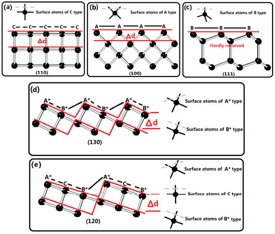
As shown in Figure 2a–c, (1 1 0), (1 0 0) and (1 1 1) planes are regarded as the three basic crystal planes of silicon, and the types of surface atoms on the three different crystal planes are marked as C, A and B, respectively. When surface atoms are directly connected by surface chemical bonds, the symbol “--” is used to indicate their connection; otherwise, the symbol “-” is used to indicate their connection. This model estimates the removal time of different combinations of surface atoms by calculating the removal time of surface atoms of three basic crystal planes. During the calculation of etch rates of silicon (the etching solution is 34 wt% KOH and the etching temperature is 71 °C), the removal time of the three types of surface atoms (C, A and B) can be calculated through etch rates of the three basic crystal planes (R(1 1 0) = 1.29 μm/min, R(1 0 0) = 0.63 μm/min and R(1 1 1) = 0.01 μm/min) and the vertical distances between the two adjacent layer of surface atoms. Since the etch rate of the (1 1 1) plane is extremely low, the removal time of surface atoms of B type can be approximated as infinite.
Surface atoms of A and B types also have A* and B* types according to their own evolution, as shown in Figure 2d,e. The difference between A type (B type) and its evolution A* type (B* type) is that angles of chemical bonds are different. Thus, atomic structures of other crystal planes can be regarded as composed of five types of surface atoms (A, A*, B, B* and C) through different combinations. As shown in Figure 2d,e, the combination of surface atoms on the (1 3 0) plane is “A*--B*”, and the combination of surface atoms on the (1 2 0) plane is “A*--C--B*”. Therefore, by reasonably analyzing the connections between surface atoms, the removal time of these different combinations of surface atoms can be estimated and etch rates of different crystal planes can be approximately gained.
As shown in Table 1, errors between calculated and experimental rates are small under the experimental condition (the etching solution is 34 wt% KOH and the etching temperature is 71 °C), which verifies the effectiveness of the layer-by-layer removal model of surface atoms (Si) under KOH solution conditions. However, due to the uncertainty of the estimation of the removal time, the accuracy of this model in calculating rates of crystal planes is low in other etching solutions (for example, KOH + IPA etchant or TMAH etchant) [26,27]. This indicates that the application of the model has certain defects. The key to improve the accuracy of the model is to propose a specific formula for calculating the removal time of the combination of surface atoms.
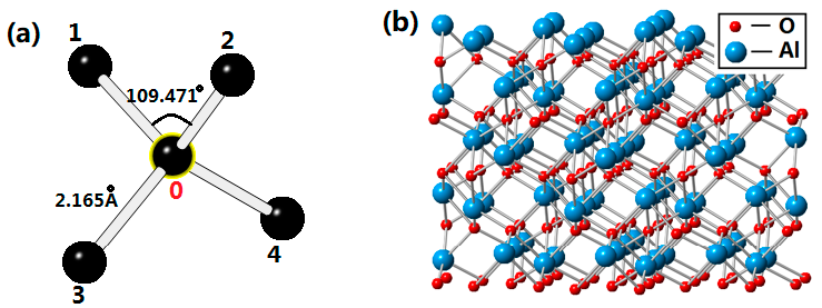
In addition, for silicon, its atomic structure is relatively simple. Therefore, it is relatively easy to estimate the removal time of different combinations of surface atoms. As shown in Figure 3a, the lengths of chemical bonds between the atom “0” and atoms “1”, “2”, “3” and “4” are all 2.165 Å. For atoms “1”, “2”, “3” and “4”, the angle between any two is 109.471°. For sapphire with a complicated atomic structure, different bond lengths and bond angles between atoms greatly increase the difficulty in estimating the removal time of different combinations of surface atoms, as shown in Figure 3b. Therefore, this paper will propose a formula to gain the removal time of different combinations of surface atoms according to the principle of this model, which can uniformly calculate the removal time of different combinations of surface atoms under different experimental conditions and avoid errors caused by estimation.
Concentrated sulfuric acid (98 wt%), concentrated phosphoric acid (87 wt%) and their mixed solutions are commonly used as etchants for sapphire, and sapphire will not react with them until the temperature is above about 200 °C [18,19,20,21,30,31,32]. The higher the temperature is, the stronger the chemical reaction is, and the quality of the etched structure of sapphire is also reduced. Therefore, considering the feasibility and processing quality of the etched structure of sapphire, the temperature is usually within the scope of 200–300 °C. When the etch solution is concentrated sulfuric acid, the insoluble deposits (Al2(SO4)3 and Al2(SO4)3·17H2O) are produced. Concentrated phosphoric acid as a buffer agent can avoid the insoluble deposits produced. When the etch solution is concentrated phosphoric acid, high temperature polymerization occurs easily. Therefore, it is reasonable to choose the mixed solution of concentrated sulfuric acid and phosphoric acid as the etchant of sapphire. In addition, when the volume ratio of the mixed solution (H2SO4 and H3PO4) is 3:1, the surface of etch structures of sapphire is smoother than that of other volume ratios [33].
The remainder of this paper includes three main sections: In Section 2, etch rate distributions in different concentration conditions are gained by the wet etching of hemispheres of sapphire. In Section 3, the atomic structure of sapphire is simplified in the right way, the arrangement laws of surface atoms of different crystal planes are analyzed and a general formula for calculating etch rates of different crystal planes is proposed. By comparing the errors between calculated and experimental rates under different concentration conditions, the effectiveness of the layer-by-layer removal model of surface atoms (Al) is verified. In Section 4, the paper is summarized.
2. Experimental Methods
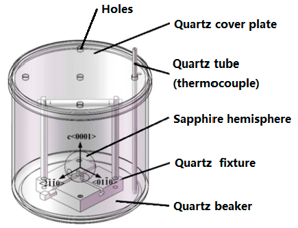
In this paper, the hemispherical etching method is used to obtain etch rates of sapphire under different experimental conditions [22,34,35]. First, sapphire crystal blocks were selected and processed into hemispherical samples with a radius of 21.5 mm, and then polished with a roughness of about 0.005 mm. Different points on the sapphire hemisphere represent different crystal planes; the top orientation of the hemisphere was <0 0 0 1> direction, and the reference crystal plane was the (1 1 −2 0) plane. The etch rate of the crystal plane was gained by calculating the ratio of the radial distance difference before and after etching to the etching time. The radial distance before and after etching can be obtained by the coordinate of the hemispherical surface position and the coordinate of the spherical center. Coordinates of the hemispherical surface can be obtained by a three dimensional coordinate measuring instrument.
The device used to etch the hemisphere of sapphire is shown in Figure 4. The etching container was a quartz beaker with a capacity of 1500 mL. The sapphire hemisphere was fixed by a fixture and placed at the bottom of the beaker. The total amount of etching solution added in the experiment was 800 mL. The cover plate was provided with small holes and placed on the top of the beaker, which prevented the steam generated during high-temperature etching from spreading around while maintaining the balance of pressure inside and outside the beaker. A thermocouple thermometer wrapped in the tube was inserted into the top of the beaker to measure the temperature of the etching solution inside the beaker. The beaker was placed on the heating panel for rapid heating.
For the purpose of analyzing the influence of concentrations of the etching solution on the anisotropy of etch rates of sapphire, three groups of hemispherical etching experiments of sapphire are designed in this paper, and the corresponding experimental parameters are shown in Table 2.
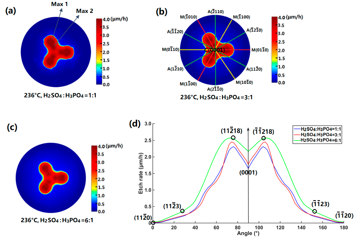
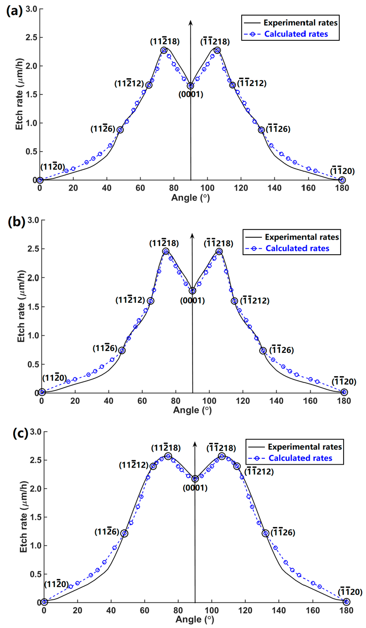
Based on the wet etching experiments of three groups of sapphire hemispheres, etch rate distributions of sapphire at different concentrations were obtained, as shown in Figure 5 [18,19,20,21,36]. It can be seen from Figure 5a–c that full etch rates of sapphire at the three different concentrations are all characterized by three-fold rotational symmetry, and the center of the rotational symmetry is the <0 0 0 1> direction. There are three groups of maximum rates (Max 1 and Max 2) in the <1 1 −2 0> crystal zone. The crystal plane positions corresponding to the maximum rates change slightly with the concentration of the etching solution, but the etch rates corresponding to the maximum rates change greatly with the concentration of the etching solution. The etch rate of the C-plane also varies with the concentration of the etching solution. The higher the proportion of concentrated sulfuric acid in the etching solution, the higher the etch rate of the C-plane. Their differences can be summarized in Table 3. It can be seen from Figure 5d that etch rates in the <−1 1 0 0> crystal zone in the different concentrations are all symmetric with respect to the <0 0 0 1> direction, and their anisotropies are very obvious. Therefore, the etch rates at three different concentrations shown in Figure 5d were selected for the anisotropic analysis of etch rates.
3. Results and Discussion
3.1. Simplification of Sapphire’s Atomic Structure
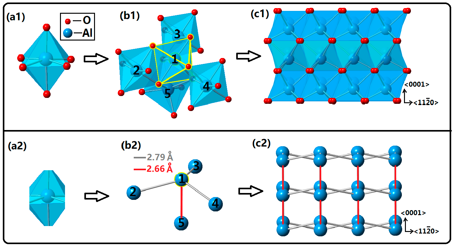
For the purpose of clearly classifying the types of surface atoms of sapphire and analyzing the arrangement laws of surface atoms of different crystal planes, it is necessary to reasonably simplify the atomic structure of sapphire [22,37]. Figure 6 is the schematic diagram of the simplified atomic structure of sapphire. As shown in Figure 6a1–c1, octahedrons can be regarded as the smallest structural units that constitute sapphire’s atomic structure, and octahedrons are linked by co-plane and co-edge ways to form sapphire’s atomic structure. Among them, octahedron one is connected with octahedrons two, three and four by co-edge way, and connected with octahedron five by co-plane way. As shown in Figure 6a2–c2, the simplified octahedron (Al) is formed by ignoring O atoms, and the co-edge and co-plane ways between octahedrons are simplified to the grey and red connections between Al atoms, thus forming the simplified atomic structure of sapphire.
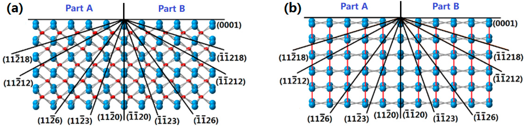
The schematic diagram of atomic structures of crystal planes in the <−1 1 0 0> crystal zone is shown in Figure 7. The schematic diagrams of atomic structures of crystal planes based on sapphire’s atomic structure in Figure 7a and the simplified sapphire atomic structure in Figure 7b both show symmetry at the <0 0 0 1> direction (that is, Part A and Part B are symmetrical at the <0 0 0 1> direction), which indicates that the simplification of sapphire’s atomic structure is reasonable. Because of the symmetry between Part A and Part B, crystal planes located in Part A can be selected for analysis.
3.2. Arrangements of Surface Atoms of Crystal Planes of Sapphire
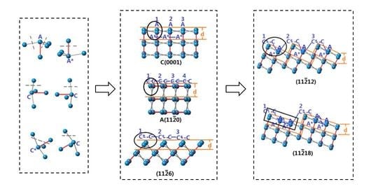
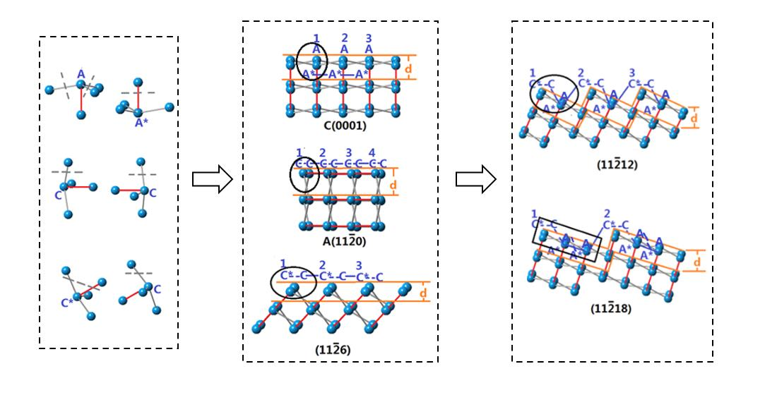
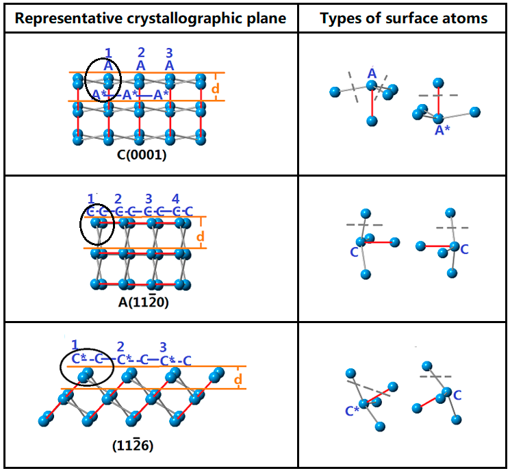
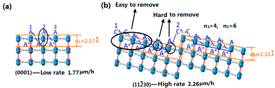
After analyzing the atomic structure of crystal planes in Part A, it was found that the arrangements of surface atoms of crystal planes have a certain regularity. Figure 8 shows the representative crystal planes C(0 0 0 1), A(1 1 −2 0) and (1 1 −2 6) in Part A, as well as the corresponding types of surface atoms A, A*, C and C*. The arrangement of surface atoms of other crystal planes in Part A can be composed of these four types of surface atoms in different combinations. Here, similarly, the symbols “--” and “-” are used to indicate the direct and indirect connections between surface atoms, respectively. The serial numbers above the crystal planes represent the repetitive arrangements of combinations of surface atoms.
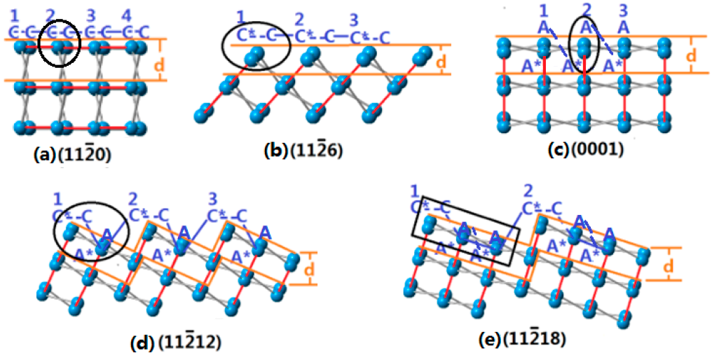
After analyzing the atomic structures of all crystal planes in Part A, it was clear that there are five basic crystal planes (1 1 −2 0), (1 1 −2 6), (0 0 0 1), (1 1 −2 12) and (1 1 −2 18) in Part A, which correspond to five basic units of surface atoms “C--C”, “C*--C”, “A*--A”, “C*--C--A*--A” and “C*--C--A*--A--A*--A”, respectively, as shown in Figure 9.
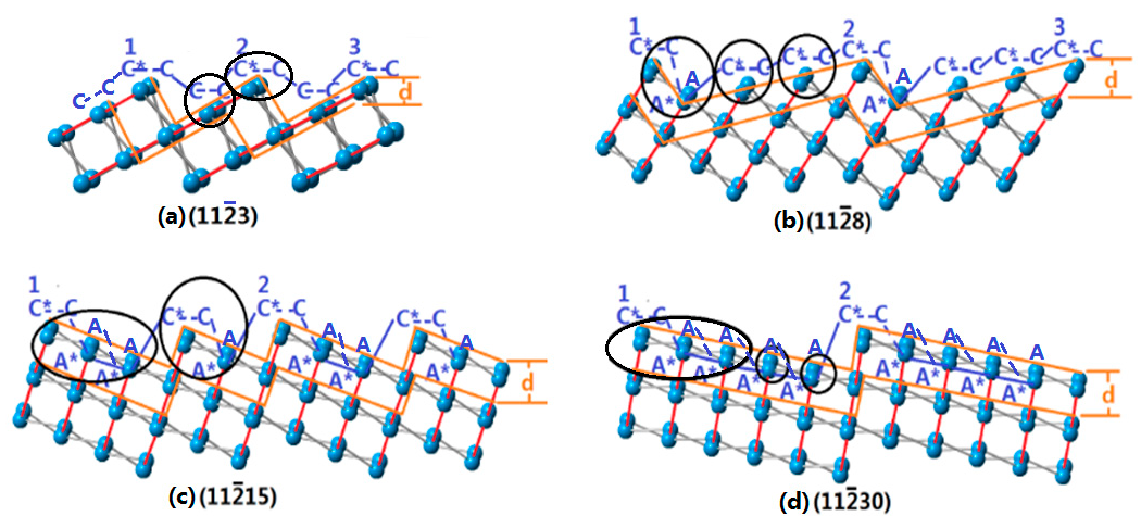
Thus, the arrangements of surface atoms of other crystal planes in Part A can be composed of these five basic units of surface atoms in different combinations, as shown in Figure 10. The arrangement of surface atoms on the (1 1 −2 3) plane can be regarded as the combination of one “C--C” and one “C*--C”. The arrangement of surface atoms on the (1 1 −2 8) plane can be regarded as the combination of one “C*--C--A*--A” and two “C*--C”. The arrangement of surface atoms on the (1 1 −2 15) plane can be regarded as the combination of one “C*--C--A*--A--A*--A” and one “C*--C--A*--A”. The arrangement of surface atoms on the (1 1 −2 30) plane can be regarded as the combination of one “C*--C--A*--A--A*--A” and two “A*--A”.
3.3. Calculation of Etch Rates of Crystal Planes of Sapphire
As shown in Figure 9, the removal time of five basic units of surface atoms is needed to further solve the removal time of different combinations composed of basic units of surface atoms. Since the rate of the (1 1 −2 0) plane is extremely low, it can be considered that the removal time of the basic unit of surface atoms “C--C” is infinite. Therefore, the removal times of the four basic units of surface atoms “C*--C”, “A*--A”, “C*--C--A*--A” and “C*--C--A*--A--A*--A” can be obtained according to the etch rates of the (1 1 −2 6), (0 0 0 1), (1 1 −2 12) and (1 1 −2 18) planes and the corresponding vertical distances between the adjacent two layers of surface atoms. The solution formula is as follows:
For the vertical distance between two adjacent layers of surface atoms of the crystal plane, it is related to the lattice parameters of the material itself and the spatial geometric position of the crystal plane. Therefore, because of the different spatial geometric positions of crystal planes, the vertical distances are different, resulting in different etch rates. The removal time of the basic unit of surface atoms determines the difficulty of its removal. In general, the larger the proportion of basic units of surface atoms with easy removal types in the combinations of surface atoms of the crystal plane is, the higher the etch rate of it is; on the contrary, the smaller the proportion is, the lower the etch rate of it is. Furthermore, based on the four basic units of surface atoms, a general formula for calculating the etch rate of the other crystal planes (non-basic crystal planes) is proposed:
Among them, and are etch rates of high and low rate crystal planes, respectively, and and are vertical distances between the adjacent two layers of surface atoms of the high and low rate crystal planes, respectively. is the rate coefficient, , , and are the numbers of surface atoms with the hard-to-remove type and the easy-to-remove type of the high-rate crystal plane, respectively, and and are the removal times of basic units of surface atoms with the hard-to-remove type and the easy-to-remove type, respectively.
For example, in the concentration condition (236 °C, H2SO4:H3PO4 = 3:1), removal times of basic units of surface atoms are calculated according to Formula (1), as shown in Table 4. Figure 11 is the schematic diagram of solving the etch rate of the (1 1 −2 30) plane when the etch rate of the basic crystal plane (0 0 0 1) is known. As shown in Figure 12 and Table 3, , , , , , and . Combined with Formula (2), the calculated rate of the (1 1 −2 30) plane is , which has a small error with the experimental rate of 2.26 μm/h.
Based on the above calculation process of the etch rate of the (1 1−2 30) plane, etch rates of all crystal planes in the <−1 1 0 0> crystal zone can be obtained. Figure 12 shows the comparisons between calculated and experimental rates in the <−1 1 0 0> crystal zone in the three different concentration conditions. The rate errors between calculated and experimental results are small, especially for the rate calculation of the high-rate crystal plane (such as the range from the (1 1 −2 6) plane to the (0 0 0 1) plane). This verifies the effectiveness of the layer-by-layer removal model of surface atoms (Al) proposed in this paper for the anisotropic analysis of etch rates of sapphire.
4. Conclusions
The layer-by-layer removal model of surface atoms (Al) established in this paper builds up a connection between etch rates and atomic structures of crystal planes of sapphire, and obtains two factors that affect the etch rates of crystal planes of sapphire: (1) the vertical distances between two adjacent layers of surface atoms of crystal planes; (2) the configurations of the types of surface atoms of crystal planes. Because of the combined effect of these two factors, anisotropic etch rates of sapphire are caused.
In this paper, according to the simplified sapphire atomic structure, the types of surface atoms are reasonably classified, which reduces the difficulty of identifying the arrangements of surface atoms of different crystal planes. A general formula for calculating etch rates of crystal planes is proposed, which builds up a connection between etch rates and atomic structures of crystal planes. Small rate errors between calculated and experimental results in the different concentration conditions verify the effectiveness of the proposed layer-by-layer removal model of surface atoms (Al). Moreover, the layer-by-layer removal model of surface atoms can offer a reference for the anisotropic analysis of etch rates of various crystal materials, such as SiO2 and GaN, to some extent.
Author Contributions
Conceptualization, G.W.; methodology, G.W.; software, Y.L.; validation, G.W. and Y.L.; formal analysis, Y.L.; investigation, G.W.; resources, G.W.; data curation, G.W.; writing—original draft preparation, G.W. and Y.L.; writing—review and editing, Y.L.; visualization, Y.L.; supervision, G.W.; project administration, G.W.; funding acquisition, G.W. and Y.L. All authors have read and agreed to the published version of the manuscript.
Funding
This research was funded by the Scientific Research Start-up Foundation for High-level Talents of Taizhou University (TZXY2022QDJJ005), the Scientific Research Start-up Foundation for High-level Talents of Taizhou University (TZXY2017QDJJ015) and the Science and Technology Support (Social Development) Project of Taizhou City (SSF20210002).
Data Availability Statement
All data are included in the study.
Acknowledgments
We thank Yan Xing, Department of Mechanical Engineering, Southeast University, for assistance with the experiments in Figure 5.
Conflicts of Interest
The authors declare no conflict of interest.
References
- Kumar, P.; Lee, J.; Lee, G.; Rao, S.; Singh, D.; Singh, R.K. Low temperature wet etching to reveal sub-surface damage in sapphire substrates. Appl. Surf. Sci. 2013, 273, 58–61. [Google Scholar] [CrossRef]
- Mu, D.K.; Feng, K.Y.; Lin, Q.L.; Huang, H. Low-temperature wetting of sapphire using Sn–Ti active solder alloys. Ceram. Int. 2019, 45, 22175–22182. [Google Scholar] [CrossRef]
- Markandan, K.; Zhang, Z.; Chin, J.K.; Cheah, K.H.; Tang, H.B. Fabrication and preliminary testing of hydroxylammonium nitrate (HAN)-based ceramic microthruster for potential application of nanosatellites in constellation formation flying. Microsyst. Technol. 2019, 25, 4209–4217. [Google Scholar] [CrossRef]
- Shang, Y.Q.; Qi, H.; Ma, Y.L.; Wu, Y.L.; Zhang, Y.; Chen, J. Study on sapphire microstructure processing technology based on wet etching. Int. J. Mod. Phys. B 2017, 31, 1741004. [Google Scholar] [CrossRef]
- Sun, C.; Zhang, Y.H.; Zheng, Y.X.; Chu, C.S.; Tian, K.K.; Fan, C.; Zhang, Z.H.; Bi, W.G. The morphology evolution of selective area wet etched commercial patterned sapphire substrates. J. Micromech. Microeng. 2019, 29, 035012. [Google Scholar] [CrossRef]
- Cao, X.W.; Lu, Y.M.; Fan, H.; Xia, H.; Zhang, L.; Zhang, Y.L. Wet-etching-assisted femtosecond laser holographic processing of a sapphire concave microlens array. Appl. Opt. 2018, 57, 9604–9608. [Google Scholar] [CrossRef]
- Wang, N. Low temperature dealloying preparation of extremely fine double-levels nano-SnO2 particles with excellent photocatalytic properties. Appl. Surf. Sci. 2020, 506, 144970. [Google Scholar] [CrossRef]
- Wang, N. Fabrication of unique Ti0.8Sn0.2O2 double-levels nanoparticles with extremely fine structure and promising photocatalytic activity by dealloying novel Cu-Ti-Sn-Y metallic glasses. Mat. Sci. Semicon. Proc. 2022, 141, 106426. [Google Scholar] [CrossRef]
- Kuo, C.T.; Hsu, L.H.; Huang, B.H.; Kuo, H.C.; Lin, C.C.; Cheng, Y.J. Influence of the microstructure geometry of patterned sapphire substrates on the light extraction efficiency of GaN LEDs. Appl. Opt. 2016, 55, 7387–7391. [Google Scholar] [CrossRef]
- Capano, L.; Tiggelaar, R.M.; Berenschot, J.W.; Gardeniers, J.G.E.; Romer, G.R.B.E. Fabrication of millimeter-long structures in sapphire using femtosecond infrared laser pulses and selective etching. Opt. Laser. Eng. 2020, 133, 106114. [Google Scholar] [CrossRef]
- Wang, G.G.; Lin, Z.Q.; Zhao, D.D.; Han, J.C. Enhanced Transmission and Self-Cleaning of Patterned Sapphire Substrates Prepared by Wet Chemical Etching Using Silica Masks. Langmuir 2018, 34, 8898–8903. [Google Scholar] [CrossRef]
- Chen, K.C.; Wuu, D.S.; Shen, C.C.; Ou, S.L. Surface Modification on Wet-Etched Patterned Sapphire Substrates Using Plasma Treatments for Improved GaN Crystal Quality and LED Performance. J. Electrochem. Soc. 2011, 158, H988–H993. [Google Scholar]
- Chen, Y.C.; Lin, B.W.; Hsu, W.C.; Wu, Y.S. Morphologies and plane indices of pyramid patterns on wet-etched patterned sapphire substrate. Mater. Lett. 2014, 118, 72–75. [Google Scholar] [CrossRef]
- Chen, C.C.; Hsiao, F.C.; Lin, B.W.; Hsu, W.C.; Wu, Y.S. Evolution of Bottom c-Plane on Wet-Etched Patterned Sapphire Substrate. ECS J. Solid State Sci. 2013, 2, R169–R171. [Google Scholar]
- Wang, N. FeCoNiMnCuTi high entropy amorphous alloys and M50Ti50 (M = Fe, Cu, FeCoNiMnCu) amorphous alloys: Novel and efficient catalysts for heterogeneous photo-Fenton decomposition of Rhodamine B. Surf. Interfaces 2022, 33, 102265. [Google Scholar] [CrossRef]
- Nakasu, T.; Aiba, T.; Yamashita, S.; Hattori, S.; Kizu, T.; Sun, W.C.; Taguri, K.; Kazami, F.; Kobayashi, M. Growth of ZnTe epilayers on r- and n-plane sapphire substrates. Jpn. J. Appl. Phys. 2015, 54, 075501. [Google Scholar] [CrossRef]
- Sakharov, A.V.; Lundin, W.V.; Zavarin, E.E.; Sinitsyn, M.A.; Nikolaev, A.E.; Lundina, E.Y.; Tsatsulnikov, A.F. Formation of textured sapphire substrates by self-arrangement process and wet etching for InGaAlN LEDs. J. Cryst. Growth 2008, 310, 5151–5153. [Google Scholar] [CrossRef]
- Shen, J.; Zhang, D.; Wang, Y.; Gan, Y. AFM and SEM Study on Crystal Topographical Evolution of Wet-Etched Patterned Sapphire Substrates (PSS): I. Cone-Shaped PSS Etched in Sulfuric Acid and Phosphoric Acid Mixture (3:1) at 230 °C. ECS J. Solid State Sci. 2017, 6, R24–R34. [Google Scholar]
- Shen, J.; Zhang, D.; Wang, Y.; Gan, Y. AFM and SEM Study on Crystal Topographical Evolutions of Wet-Etched Patterned Sapphire Substrate (PSS): Part III. Cone-Shaped PSS Etched in H2SO4 and H3PO4 Mixture at Various Temperatures. ECS J. Solid State Sci. 2017, 6, R163–R169. [Google Scholar]
- Shen, J.; Zhang, D.; Wang, Y.; Gan, Y. AFM and SEM Study on Crystal Topographical Evolutions of Wet-Etched Patterned Sapphire Substrate (PSS): Part II. Cone-Shaped PSS Etched in H2SO4 and H3PO4 Mixture with Varying Volume Ratio at 230 °C. ECS J. Solid State Sci. 2017, 6, R122–R130. [Google Scholar]
- Aota, N.; Aida, H.; Kimura, Y.; Kawamata, Y.; Uneda, M. Fabrication Mechanism for Patterned Sapphire Substrates by Wet Etching. ECS J. Solid State Sci. 2014, 3, N69–N74. [Google Scholar] [CrossRef]
- Wu, G.R.; Xing, Y.; Chen, Y.; Zhou, Z.F. Application of the evolutionary kinetic Monte Carlo method for the simulation of anisotropic wet etching of sapphire. J. Micromech. Microeng. 2021, 31, 065001. [Google Scholar] [CrossRef]
- Zhou, Z.F.; Huang, Q.A.; Li, W.H. Modeling and Simulations of Anisotropic Etching of Silicon in Alkaline Solutions with Experimental Verification. J. Electrochem. Soc. 2009, 156, F29–F37. [Google Scholar] [CrossRef]
- Pal, P.; Sato, K.; Gosalvez, M.A.; Kimura, Y.; Ishibashi, K.I.; Niwano, M.; Hida, H.; Tang, B.; Itoh, S. Surfactant Adsorption on Single-Crystal Silicon Surfaces in TMAH Solution: Orientation-Dependent Adsorption Detected by In Situ Infrared Spectroscopy. J. J. Microelectromech. Syst. 2009, 18, 1345–1356. [Google Scholar] [CrossRef]
- Zubel, I. The influence of atomic configuration of (h k l) planes on adsorption processes associated with anisotropic etching of silicon. Sens. Actuat. A-Phys. 2001, 94, 76–86. [Google Scholar] [CrossRef]
- Biswas, K.; Kal, S. Etch characteristics of KOH, TMAH and dual doped TMAH for bulk micromachining of silicon. Microelectron. J. 2006, 37, 519–525. [Google Scholar] [CrossRef]
- Kramkowska, M.; Zubel, I. Silicon anisotropic etching in KOH and TMAH with modified surface tension. Procedia Chem. 2009, 1, 774–777. [Google Scholar] [CrossRef]
- Rola, K.P.; Zubel, I. Effect of molecular structure of alcohols on wet anisotropic etching of silicon. Sens. Actuat. A-Phys. 2016, 242, 18–26. [Google Scholar] [CrossRef]
- Zubel, I. The Model of Etching of (hkl) Planes in Monocrystalline Silicon. J. Electrochem. Soc. 2003, 150, C391–C400. [Google Scholar] [CrossRef]
- Shin, H.Y.; Kwon, S.K.; Chang, Y.I.; Cho, M.J.; Park, K.H. Reducing dislocation density in GaN films using a cone-shaped patterned sapphire substrate. J. Cryst. Growth 2009, 311, 4167–4170. [Google Scholar] [CrossRef]
- Lin, R.M.; Lu, Y.C.; Yu, S.F.; Wu, Y.S.; Chiang, C.H.; Hsu, W.C.; Chang, S.J. Enhanced Extraction and Efficiency of Blue Light-Emitting Diodes Prepared Using Two-Step-Etched Patterned Sapphire Substrates. J. Electrochem. Soc. 2009, 156, H874–H876. [Google Scholar] [CrossRef]
- Cuong, T.V.; Cheong, H.S.; Kim, H.G.; Kim, H.Y.; Hong, C.H.; Suh, E.K.; Cho, H.K.; Kong, B.H. Enhanced light output from aligned micropit InGaN-based light emitting diodes using wet-etch sapphire patterning. Appl. Phys. Lett. 2007, 90, 131107. [Google Scholar] [CrossRef]
- Wang, J.; Guo, L.W.; Jia, H.Q.; Wang, Y.; Xing, Z.G.; Li, W.; Chen, H.; Zhou, J.M. Fabrication of Patterned Sapphire Substrate by Wet Chemical Etching for Maskless Lateral Overgrowth of GaN. J. Electrochem. Soc. 2006, 153, C182–C185. [Google Scholar] [CrossRef]
- Sato, K.; Shikida, M.; Matsushima, Y.; Yamashiro, T.; Asaumi, K.; Iriye, Y.; Yamamoto, M. Characterization of orientation-dependent etching properties of single-crystal silicon: Effects of KOH concentration. Sens. Actuat. A-Phys. 1998, 64, 87–93. [Google Scholar] [CrossRef]
- Sato, K.; Shikida, M.; Yamashiro, T.; Tsunekawa, M.; Ito, S. Roughening of single-crystal silicon surface etched by KOH water solution. Sens. Actuat. A-Phys. 1999, 73, 122–130. [Google Scholar] [CrossRef]
- Toifl, A.; Quell, M.; Klemenschits, X.; Manstetten, P.; Hossinger, A.; Selberherr, S.; Weinbub, J. Continuum level-set model for anisotropic wet etching of patterned sapphire substrates. IEEE Access 2020, 8, 115406. [Google Scholar] [CrossRef]
- Ferrando, N.; Gosalvez, M.A.; Colom, R.J. Evolutionary continuous cellular automaton for the simulation of wet etching of quartz. J. Micromech. Microeng. 2012, 22, 025021. [Google Scholar] [CrossRef]
Figure 1.
The schematic diagram of the layer-by-layer removal model of surface atoms [29].
Figure 1.
The schematic diagram of the layer-by-layer removal model of surface atoms [29].

Figure 2.
(a–c) Atomic structures and types of surface atoms of the three basic crystal planes (1 1 0), (1 0 0) and (1 1 1) of silicon; (d,e) atomic structures and types of surface atoms of other crystal planes (1 3 0) and (1 2 0) of silicon [29].
Figure 2.
(a–c) Atomic structures and types of surface atoms of the three basic crystal planes (1 1 0), (1 0 0) and (1 1 1) of silicon; (d,e) atomic structures and types of surface atoms of other crystal planes (1 3 0) and (1 2 0) of silicon [29].

Figure 3.
(a) The smallest structural unit of silicon; (b) atomic structure of sapphire.

Figure 4.
The schematic diagram of the wet etching device used to etch the hemisphere of sapphire.

Figure 5.
(a–c) Etch rate distributions of sapphire under different concentrations (236 °C, H2SO4:H3PO4 = 1:1, 3:1 and 6:1); (d) etch rate in the <−1 1 0 0> crystal zone under different concentrations (236 °C, H2SO4:H3PO4 = 1:1, 3:1 and 6:1).
Figure 5.
(a–c) Etch rate distributions of sapphire under different concentrations (236 °C, H2SO4:H3PO4 = 1:1, 3:1 and 6:1); (d) etch rate in the <−1 1 0 0> crystal zone under different concentrations (236 °C, H2SO4:H3PO4 = 1:1, 3:1 and 6:1).

Figure 6.
The schematic diagram of the simplified sapphire atomic structure: (a1) one octahedron includes one Al and six O atoms; (b1) the co-plane and co-edge ways of octahedrons; (c1) the non-simplified sapphire atomic structure; (a2) the octahedron that has been simplified (ignoring O atoms); (b2) the grey and red connections between Al atoms that correspond to the co-edge and co-plane ways between octahedrons; (c2) the sapphire atomic structure that has been simplified.

Figure 7.
The schematic diagram of atomic structures of different crystal planes in the <−1 1 0 0> crystal zone: (a) based on the atomic structure of sapphire; (b) based on the simplified atomic structure of sapphire.
Figure 7.
The schematic diagram of atomic structures of different crystal planes in the <−1 1 0 0> crystal zone: (a) based on the atomic structure of sapphire; (b) based on the simplified atomic structure of sapphire.

Figure 8.
Atomic structures and types of surface atoms of representative crystal planes in Part A.

Figure 9.
Atomic structures and types of surface atoms of basic crystal planes in Part A: (a) (1 1 −2 0) plane; (b) (1 1 −2 6) plane; (c) (0 0 0 1) plane; (d) (1 1 −2 12) plane; (e) (1 1 −2 18) plane.
Figure 9.
Atomic structures and types of surface atoms of basic crystal planes in Part A: (a) (1 1 −2 0) plane; (b) (1 1 −2 6) plane; (c) (0 0 0 1) plane; (d) (1 1 −2 12) plane; (e) (1 1 −2 18) plane.

Figure 10.
Atomic structures and types of surface atoms of the other crystal planes in Part A: (a) (1 1 −2 3); (b) (1 1 −2 8); (c) (1 1 −2 15); (d) (1 1 −2 30).
Figure 10.
Atomic structures and types of surface atoms of the other crystal planes in Part A: (a) (1 1 −2 3); (b) (1 1 −2 8); (c) (1 1 −2 15); (d) (1 1 −2 30).

Figure 11.
The schematic diagram of solving the etch rate of the (1 1 −2 30) plane when the etch rate of the basic crystal plane (0 0 0 1) is known: (a) (0 0 0 1); (b) (1 1 −2 30).
Figure 11.
The schematic diagram of solving the etch rate of the (1 1 −2 30) plane when the etch rate of the basic crystal plane (0 0 0 1) is known: (a) (0 0 0 1); (b) (1 1 −2 30).

Figure 12.
The comparisons between calculated and experimental rates in the <−1 1 0 0> crystal zone in the three different concentration conditions: (a) 236 °C, H2SO4:H3PO4 = 1:1; (b) 236 °C, H2SO4:H3PO4 = 3:1; (c) 236 °C, H2SO4:H3PO4 = 6:1.
Figure 12.
The comparisons between calculated and experimental rates in the <−1 1 0 0> crystal zone in the three different concentration conditions: (a) 236 °C, H2SO4:H3PO4 = 1:1; (b) 236 °C, H2SO4:H3PO4 = 3:1; (c) 236 °C, H2SO4:H3PO4 = 6:1.


Table 1.
Calculated and experimental rates of crystal planes under the experimental condition (the etching solution is 34 wt% KOH and the etching temperature is 71 °C) [29].
Table 1.
Calculated and experimental rates of crystal planes under the experimental condition (the etching solution is 34 wt% KOH and the etching temperature is 71 °C) [29].
| Crystal Planes | (2 2 1) | (3 3 1) | (2 1 0) | (3 1 0) | (3 2 0) |
|---|---|---|---|---|---|
| Experimental rates (μm/min) | 0.59 | 0.85 | 1.24 | 1.08 | 1.28 |
| Calculated rates (μm/min) | 0.61 | 0.83 | 1.22 | 1.15 | 1.26 |
Table 2.
Experimental parameters of the wet etching of sapphire hemispheres at different concentrations (volume ratios of 98 wt% H2SO4 to 87 wt% H3PO4).
Table 2.
Experimental parameters of the wet etching of sapphire hemispheres at different concentrations (volume ratios of 98 wt% H2SO4 to 87 wt% H3PO4).
| Group | Concentration | Temperature (°C) | Time (h) |
|---|---|---|---|
| 1 | H2SO4:H3PO4 = 1:1 | 236 | 24 |
| 2 | H2SO4:H3PO4 = 3:1 | 236 | 24 |
| 3 | H2SO4:H3PO4 = 6:1 | 236 | 24 |
Table 3.
Maximum rates (Max 1 and Max 2) at different concentrations (volume ratios of 98 wt% H2SO4 to 87 wt% H3PO4).
Table 3.
Maximum rates (Max 1 and Max 2) at different concentrations (volume ratios of 98 wt% H2SO4 to 87 wt% H3PO4).
| Concentration | (0 0 0 1) (μm/h) | Max 1 (μm/h) | Max 2 (μm/h) |
|---|---|---|---|
| H2SO4:H3PO4 = 1:1 | 1.65 | 3.40 (1 −1 0 10) | 3.96 (1 −1 0 4) |
| H2SO4:H3PO4 = 3:1 | 1.77 | 3.11 (1 −1 0 11) | 2.97 (1 −1 0 4) |
| H2SO4:H3PO4 = 6:1 | 2.17 | 3.28 (1 −1 0 11) | 2.54 (1 −1 0 4) |
Table 4.
Removal times of basic units in the concentration condition (236 °C, H2SO4:H3PO4 = 3:1).
| Basic Unit of Surface Atoms | C*--C | A*--A | C*--C--A*--A | C*--C--A*--A--A*--A |
|---|---|---|---|---|
| Corresponding basic crystal planes | (1 1 −2 6) | (0 0 0 1) | (1 1 −2 12) | (1 1 −2 18) |
| Vertical distances between two adjacent layers of surface atoms (Å) | 1.61 | 2.17 | 1.98 | 2.08 |
| Etch rates (μm/h) | 0.74 | 1.77 | 1.71 | 2.42 |
| Removal times (10−4 h) | 2.18 | 1.23 | 1.16 | 0.85 |
Disclaimer/Publisher’s Note: The statements, opinions and data contained in all publications are solely those of the individual author(s) and contributor(s) and not of MDPI and/or the editor(s). MDPI and/or the editor(s) disclaim responsibility for any injury to people or property resulting from any ideas, methods, instructions or products referred to in the content. |
© 2023 by the authors. Licensee MDPI, Basel, Switzerland. This article is an open access article distributed under the terms and conditions of the Creative Commons Attribution (CC BY) license (https://creativecommons.org/licenses/by/4.0/).
Share and Cite
MDPI and ACS Style
Li, Y.; Wu, G. Anisotropic Analysis of Etch Rates for Sapphire Based on a Layer-by-Layer Removal Model of Surface Atoms. Processes 2023, 11, 1290. https://doi.org/10.3390/pr11041290
AMA Style
Li Y, Wu G. Anisotropic Analysis of Etch Rates for Sapphire Based on a Layer-by-Layer Removal Model of Surface Atoms. Processes. 2023; 11(4):1290. https://doi.org/10.3390/pr11041290
Chicago/Turabian StyleLi, Yang, and Guorong Wu. 2023. "Anisotropic Analysis of Etch Rates for Sapphire Based on a Layer-by-Layer Removal Model of Surface Atoms" Processes 11, no. 4: 1290. https://doi.org/10.3390/pr11041290
Note that from the first issue of 2016, this journal uses article numbers instead of page numbers. See further details here.