Article

A Novel Dead Time Design Method for Full-Bridge LLC Resonant Converters with SiC Semiconductors

1
School of Automation, Guangxi University of Science and Technology, Liuzhou 545000, China
2
Guangxi Key Laboratory of Auto Parts and Vehicle Technology, Guangxi University of Science and Technology, Liuzhou 545000, China
3
School of Electronic Engineering, Guangxi University of Science and Technology, Liuzhou 545000, China
*
Author to whom correspondence should be addressed.
Processes 2023, 11(3), 973; https://doi.org/10.3390/pr11030973
Submission received: 23 February 2023 / Revised: 20 March 2023 / Accepted: 21 March 2023 / Published: 22 March 2023
(This article belongs to the Section Energy Systems)

Abstract

:
As third-generation semiconductors become commercial, SiC semiconductors are gradually becoming more widely used in LLC resonant converters. The efficiency of the LLC resonant converter is improved by employing soft switching. However, when designing LLC resonant converters, semiconductors are usually regarded as ideal devices, and their turn-on and turn-off times are neglected. Furthermore, the method of designing the dead time relies on engineering experience and lacks precise theoretical foundations. In order to overcome the shortcomings of the current empirical method and to improve the generality and practicality of the dead time design method, a novel method for calculating the dead time of full-bridge LLC converters is proposed through theoretical research based on the operating principle of full-bridge LLC converters and the conditions for implementing soft switching. The method takes into account the switching characteristics of semiconductors and the on-state delay time of their body diodes, stray inductance, drive circuits, and errors arising from the first harmonic approximation (FHA) and improves the accuracy of the dead time calculation. It can implement good soft switching with full-bridge LLC converters, reduce switching losses, and improve system efficiency. Finally, the simulation experiment and the 2 kW experimental prototype are built to verify the effectiveness of the proposed method.

1. Introduction

Due to the limitations of new energy sources themselves, a DC-DC converter is generally required to achieve a stable and continuous conversion of energy. In recent years, DC-DC converters have been rapidly developed with the development of new energy technologies [1,2], especially in new energy vehicles [3]. Among the converter topologies that have emerged, the LLC resonant converter topology has attracted much attention for its soft switching and wide range of voltage regulation. LLC resonant converters have high efficiency when they are operated at a resonant frequency. And their high switch frequency is conducive to reducing the size of magnetizing components. At the same time, a higher switching frequency is beneficial to improve the dynamic response of the converter. Scholars have carried out various research on the operating principle [4,5,6], loss analysis [7] and dead time [8,9,10,11,12,13,14] of LLC resonant converters.
Silicon carbide (SiC) and gallium nitride (GaN) semiconductors representing third- generation semiconductors are gradually being used in DC-DC converters due to their superior performance. SiC materials have three times the band gap width and nearly 10 times the dielectric breakdown strength compared to silicon (Si) materials; therefore, SiC semiconductors possess superior resistance to pressure and irradiation [15], have higher withstand voltage values, and switch frequency, while greatly reducing their conduction losses [16,17]. SiC semiconductors operate stably even at high frequencies due to the double electron saturation and axial drift rate of SiC. Moreover, their excellent thermal conductivity enables them to operate at much higher temperatures. In summary, SiC semiconductors can operate at high voltages, high powers, high frequencies, and high temperatures [18,19,20]. Therefore, the application of SiC semiconductors to DC-DC converters is beneficial in improving the power density and reducing the switching losses of the converters, etc.
SiC semiconductors have a certain time delay in the shutdown process. When used in full-bridge LLC resonant converters, it is often necessary to set an appropriate dead time to avoid simultaneous conduction of the upper and lower SiC semiconductors in the same bridge arm, thus improving the safety of the converter operation [21]. Moreover, the appropriate length of dead time allows the converter to achieve soft switching, reducing losses, and optimizing efficiency. However, if the dead time is too long, it will lead to distortion of the output waveform and a reduction in efficiency, while a short dead time will reduce the reliability of LLC resonant converters. The method commonly used in engineering is to select the dead time based on experience in a wide range of tens to hundreds of nanoseconds; then, on the basis of the relationship among the magnetizing inductance, dead time, and ZVS (zero voltage switch), the selected dead time is used to calculate the magnitude of the magnetizing inductance to confirm whether it can realize ZVS [9,10,11]; if so, the selection of the dead time is completed; otherwise, all operations are repeated. This method is simple to calculate, highly practical in engineering, and easy to design the parameters of the converter, but it lacks accuracy. Different operating conditions of the converter result in different current flows through the magnetizing inductor. Therefore, the parasitic capacitors charging and discharging times are also different, and the dead time should be varied as well. The dead time calculated by the above method is fixed, so the loss of semiconductors will be greatly increased under certain conditions. In [12], time domain analysis is used to calculate the exact dead time of the LLC resonant converters and to determine the minimum dead time to achieve the ZVS by selecting a normalized maximum switching frequency. The method has a higher degree of accuracy, but it is difficult to apply in practical engineering because of the number of complicated calculations involved. In [13], the effect of the semiconductor turn-off process on the dead time is considered, and the minimum dead time required under the worst operating conditions is accurately calculated. A high degree of accuracy can be achieved with this method, but it requires simulation software and the datasheets of the semiconductors to calculate the relevant parameters. There will be some errors in the calculation since the parameters in the datasheet are derived from the corresponding scenarios rather than the actual application scenarios. Simulation software performs numerical calculations in an ideal environment, while the prototype will produce deviations when the simulated values are brought into it for calculation. In addition, the method proposed in [13] considers the parameters of the actual circuit, such as the driving resistance, which leads to a complex and tedious calculation process and lacks universality. In [22], an adaptive dead time design method for LLC resonant converters is proposed for the application scenario of energy routers. In this method, the dead time can be dynamically adjusted according to the operating conditions of the energy routers without having to calculate the dead time accurately, taking into account the body diode loss of semiconductors. As a result, the LLC resonant converter’s efficiency at light load can be improved, but real-time voltage acquisition between the drain and source of the semiconductors (VDS) is required, which requires high sensitivity and accuracy of the sampling circuit, and the controller design is quite complex. Based on double-pulse tests, SiC semiconductors have better switching performance than Si semiconductors [23]. However, a strict dead time calculation equation is given considering the node capacitor of SiC semiconductors and the stray capacitance of the circuit, and experiments show that SiC semiconductors lose ZVS once the dead time deviates from the calculated time. This method is simple to calculate and easy to implement. However, the actual switching characteristics of SiC semiconductors, such as on and off delays, are ignored. However, stray inductance has an effect on ZVS, but only the effect of stray capacitance is considered in [23].
The paper proposes a novel method for designing the dead time of LLC converters, focusing on the switching characteristics of SiC MOSFETs and the time delay characteristics of driver circuits as well as errors generated by FHA. This method is widely applicable. The dead time is usually set between tens and hundreds of nanoseconds, whereas the on-state delay of the diode is usually between a few nanoseconds and hundreds of nanoseconds, so its effect cannot be completely ignored, but in the above papers, the on-state delay time of the diode is mostly ignored. In addition, the FHA used to derive the minimum dead time in the above-mentioned papers has some errors that lead to inaccurate calculation results. The design method proposed in this paper remedies the above-mentioned defects and derives the equation for dead time calculation. At the same time, the effects of various types of interference, such as stray inductance and stray capacitance in the driver circuit, are also considered. To improve the accuracy of the calculation, a margin is added to the calculated minimum dead time to ensure that the LLC resonant converters can achieve ZVS regardless of operating conditions.
The remainder of the paper is structured as follows: in Section 2, the operating modes of the LLC resonant converter and the principle of ZVS implementation are analyzed. Based on the above analysis, the relationship between dead time and ZVS is derived in detail, and the design steps of dead time are introduced in Section 3. Section 4 describes the parameters of the experimental prototype as well as the presentation and analysis of the experimental results. Section 5 draws the main conclusions of the paper.

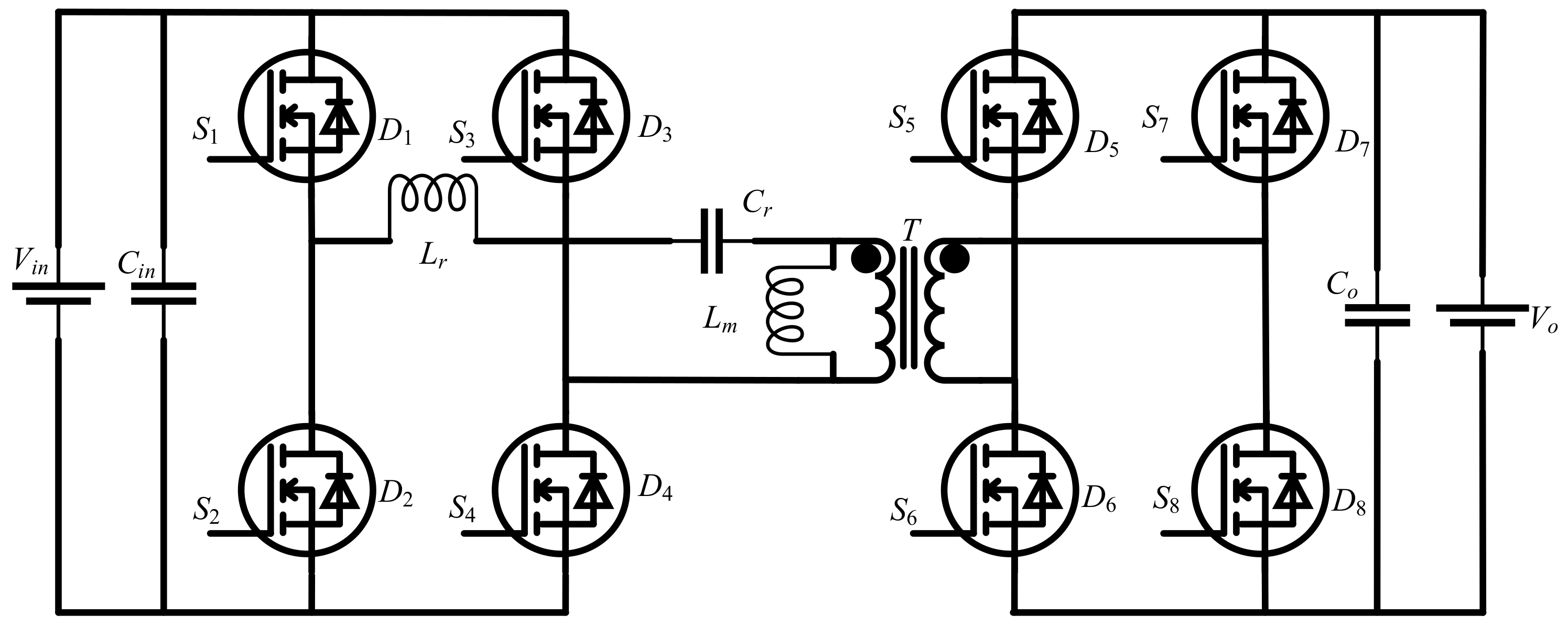
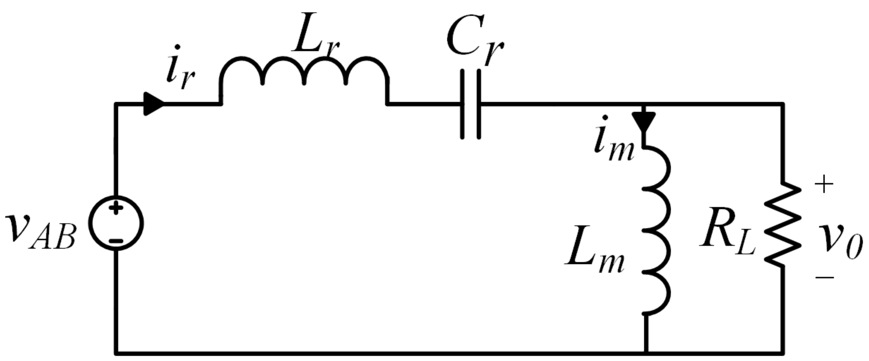
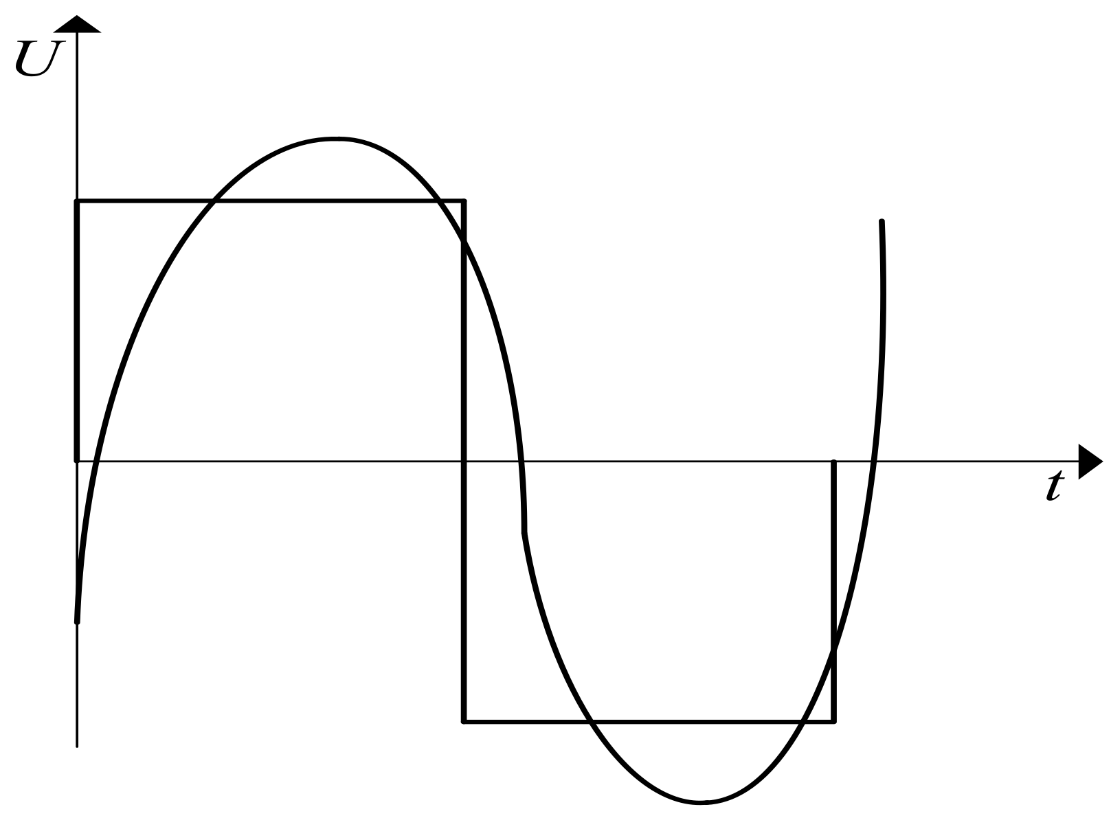
2. Analysis of the Full-Bridge LLC Resonant Converter

The full-bridge LLC resonant converter topology is shown in Figure 1. This topology is mainly composed of semiconductors S1~S4 and corresponding body diodes and parasitic capacitors, a resonant inductor Lr, a resonant capacitor Cr, a magnetizing inductor Lm, a transformer T, and rectifier diodes D5~D8, and constitutes two resonant tunes with resonant frequencies fr and fm, respectively:
f r = 1 2 π L r C r
f m = 1 2 π L r + L m C r
When the converter works in the first half cycle, S1 and S4 are turned on. The resonant current Ir flows through Lr, Cr, and the primary winding of the transformer through S1 and S4. At first, Lm is clamped by the output voltage and does not participate in resonance, so the magnetizing current Im increases linearly. When the difference between the magnetizing current and the resonant current flows to the secondary side, it provides energy to the load R through D5 and D8. The secondary output is short-circuited when the magnetizing current and resonance current are equal, and no more energy is supplied to the load R. The second half of the cycle is similar to this process and will not be repeated. In addition, the operating waveform of the converter is closely related to the switching frequency fs, which is mainly discussed in the following cases.
(1)
When fm < fsfr, the semiconductors on both the primary and secondary sides can realize soft switching. The discharge of C2 and C3 begins after Ir = Im, as shown in Figure 2a,b. As S2 and S3 drain-source voltages are clamped to zero, D2 and D3 start to conduct (the actual diode has a voltage drop of 0.6 to 0.8 V, which is approximated to zero), thus preparing S2 and S3 to achieve ZVS. At this point, no current flows through the primary side of the transformer, and the secondary current gradually decreases to zero, so D5 and D8 achieve ZCS. It can be deduced that the dead time must be greater than the sum of the capacitor discharge time and the diode conduction time, and the energy stored in Lr and Lm must be greater than the energy stored in Cr to ensure that the direction of the current will not change due to the capacitor discharge, otherwise, D2, D3, cannot be conducted.
(2)
When fs > fr, only S1~S4 can achieve soft switching. C2 and C3 are discharged, and Ir drops rapidly, making the process time of Ir dropping to Im shorter and preparing for the realization of ZVS. However, since Ir > Im during the dead time, there is still current flowing to the secondary side, resulting in D5~D8 not achieving ZCS.

3. The Calculation Method of Dead Time

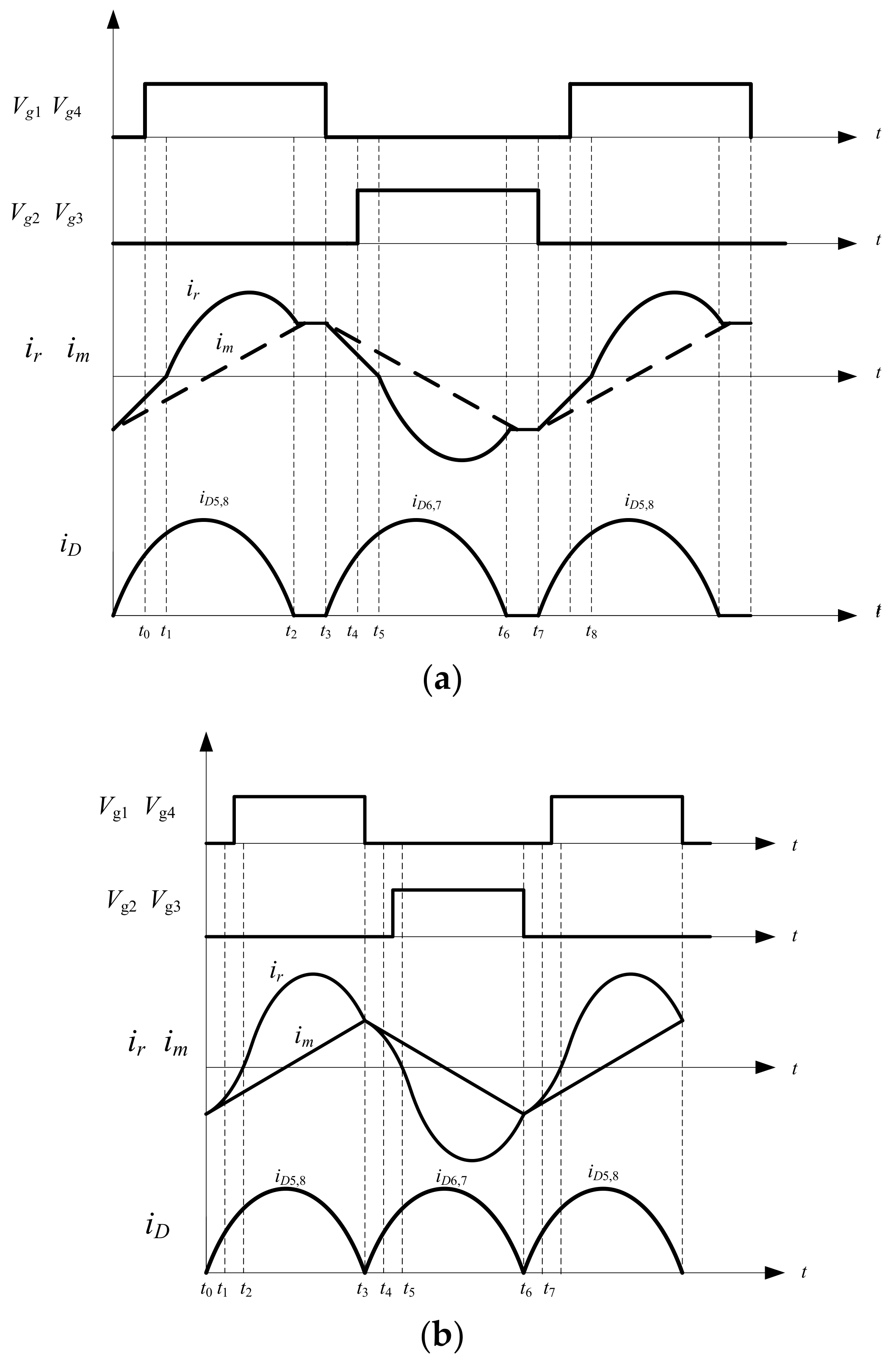
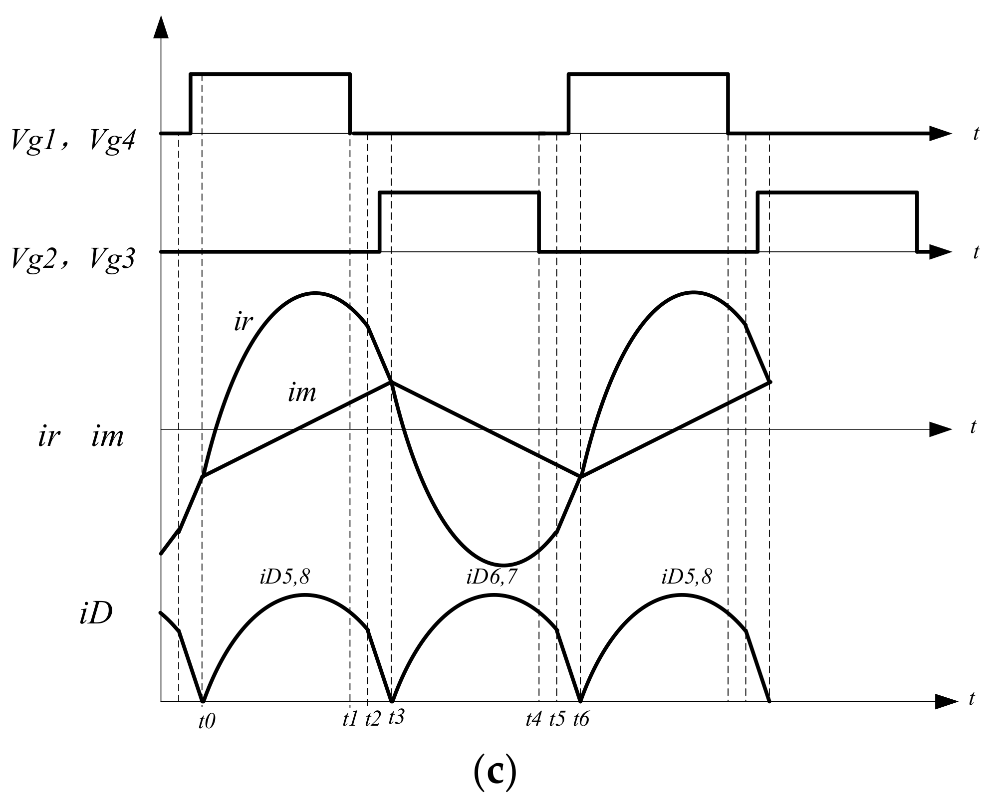
3.1. Calculation of Dead Time in Boost Mode

The circuit of the full-bridge LLC resonant converter is shown in Figure 1, where the input voltage Vin is inverted by the semiconductors S1, S4, and S2, S3, and the primary input voltage becomes a square wave of amplitude Vin [24], which is then expanded by Fourier expansion as shown as follows:
v A B t = 4 π V i n n = 1 , 3 , 5 1 n sin 2 n π f s t
The fundamental wave component of v A B is obtained using Fourier expansion and FHA as:
v s t = 4 π × V i n × sin 2 π f s t
Similarly, the output-side voltage is also a square-wave voltage, whose fundamental component is:
v e t = 4 π × n × V 0 × sin 2 π f s t φ
where n is the transformer ratio; V 0 is the output voltage; and φ is the phase difference between v e and v s .
The current flowing through the magnetizing inductor is:
i m t = v e t ω L m = 4 π × n × V 0 × sin 2 π f s t φ 2 π f s L m
According to the above analysis, Figure 3 shows the equivalent circuit for a full-bridge LLC resonant converter [25], while Figure 4 shows how the square wave voltage is related to the fundamental component determined by FHA. According to the operating principle of a full-bridge LLC resonant converter, it is known that the resonant current is equal to the magnetizing current in the dead time. The energy stored in the resonant inductor and the magnetizing inductor is converted to the energy needed to charge and discharge the parasitic capacitors, i.e., it is able to charge the parasitic capacitor of S1 and discharge the parasitic capacitor of S2 before the body diode of S2 is conducted. Since the resonant capacitor Cr is much larger than the two parasitic capacitors, the energy conversion of Cr is negligible. In order to realize the ZVS of the primary semiconductors, the parasitic capacitor of the semiconductors must be fully charged and discharged during the dead time. Therefore, when the magnetizing current rises to its maximum, the energy stored in the magnetizing inductor and the resonant inductor must be greater than the energy stored in the parasitic capacitors. As a result, Equations (7) and (8) must be satisfied in order for the diode to conduct during the dead time.
1 2 L r + L m × I m _ p 2 1 2 2 C d s × V i n 2
t c C d s × V i n / I m _ p
where Lr is the value of the resonant inductance; Lm is the value of the magnetizing inductance; Im_p is the maximum value of the magnetizing current; Cds is the parasitic capacitor of the semiconductors; and t c is the discharge time of the parasitic capacitor.
As the full-bridge LLC resonant converter conducts two semiconductors simultaneously, there are two capacitors discharged at the same time. Then the minimum discharge time of the parasitic capacitor of the full-bridge LLC resonant converter is:
t c = 16 × C d s × f s × L m
Semiconductors are assumed in all the above analyses to be ideal devices and to be instantaneous, ignoring the fact that they turn on and off. In the actual application, semiconductors also have a certain on-and-off time delay due to the semiconductors themselves and the drive circuit. Although this time delay is very small, it should not be ignored from a security analysis. To improve applicability, the time delay td to prevent simultaneous conduction of two semiconductors on the top and bottom of the same bridge arm is calculated mainly from the datasheet.
t d = t d _ o n + t r t d _ o f f t f
where td_on is the on-delay time; tr is the on-rise time; td_off is the off-delay time; and tf is the off-fall time.
Moreover, the body diode of the SiC semiconductor has a certain turn-on time tdiode because it is very small and usually ignored, the body diode is switched on instantaneously by default. However, in the actual circuit, tdiode is easily affected by the stray inductance near the semiconductor, which usually varies from tens to hundreds of nanoseconds. And the dead time is usually designed around a few hundred nanoseconds, so tdiode should not be ignored when designing the dead time. According to the above analysis, the dead time for a full-bridge LLC resonant converter must be longer than the sum of the capacitor discharge time, the diode delay time, and the turn-on time. Since the full-bridge circuit has two semiconductors on and off, the dead time is:
t d e a d 2 t c + t d + t d i o d e
The error from FHA can be derived from Figure 4. The equivalent voltage maximum is about 4/π (about 1.3) of the actual value, so the peak magnetizing current is greater than the actual value, and the calculated capacitor charging and discharging time is less than the actual time [26,27]. Consequently, the dead time calculated by Equation (11) is somewhat smaller, and an increase factor of 1.5 is taken into account when considering the overall effect of FHA as described above. So:
t d e a d 1.5 × 2 × t c + t d i o d e + 2 t d
During the operation of the actual circuit, there are various disturbances, such as driver circuits, parasitic capacitance, and stray inductance. In addition, there are various types of disturbances in the actual operation of the converter, such as the delay of the drive circuit, so the margin α is added to Equation (12) to make tdead still meet the requirements under various types of disturbances.
t d e a d = 1 + α × 1.5 × 2 × t c + t d i o d e + 2 t d
So,
t d e a d = 1 + α × 3 t c + t d i o d e + 2 t d
where α is the margin, generally taken as 10% [13].

3.2. Calculation of Dead Time in Buck Mode

The converter operates in buck mode, with the current slightly ahead of the voltage. During the dead time, the magnetizing inductor Lm is clamped not to participate in resonance, and the resonant current forms a loop; thus, the current flowing through the parasitic capacitor in Equation (7) is the resonant current. After the semiconductors are turned off, the resonant current is subjected to factors such as parasitic capacitors that accelerate the downward trend, and the calculation is complicated. To simplify the analysis, the maximum of the magnetizing current is used instead of the resonance current. However, the result on the right side of Equation (14) needs to be increased to ensure a sufficiently large dead time. In buck mode, therefore, the dead time is similar to Equation (14), and only the margin needs to be adjusted.

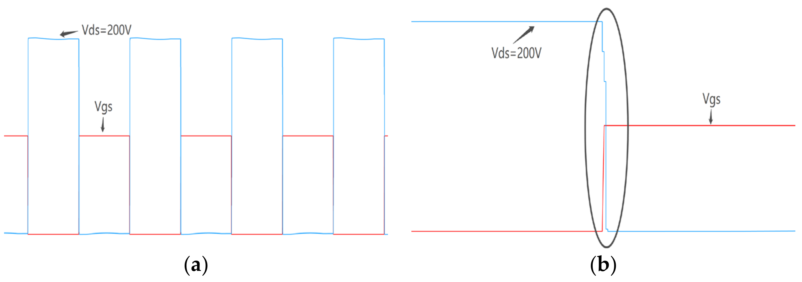
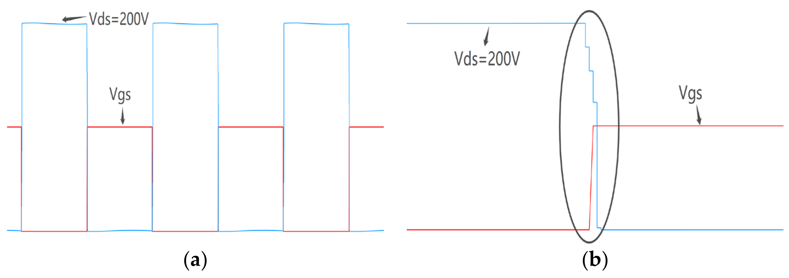
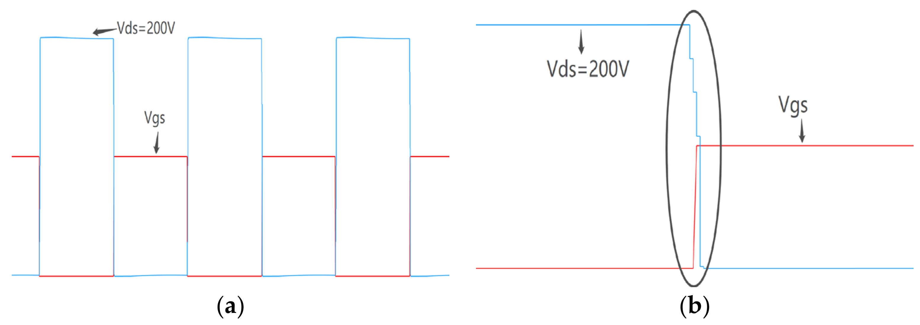
4. Experimental Validation and Analysis of Results

4.1. Calculation of Experimental Parameters

As shown in Figure 5, a 2 kW experimental prototype was designed and built to verify the proposed dead time design method. The main specifications of the prototype are given in Table 1, and the power stage component parameters are listed in Table 2.
For the purpose of verifying the dead time design method described in this paper, three switching frequency points of 100 kHz, 125 kHz, and 140 kHz were chosen based on the operating characteristics of the experimental prototype. First, by consulting the data sheet of the selected SiC semiconductor to get its body diode conduction time and parasitic capacitor’s value, these data will be brought into Equation (14) to calculate the dead time corresponding to the above three frequency points, and the value of α is 10%. To compare the superiority of the method proposed in this paper, the dead time of the corresponding three frequency points was also calculated using the method in [11]. All calculation results are shown in Table 3. The results obtained by the method proposed in this paper are much larger than those obtained by the method used in [11]. Moreover, the results in [11] only give a small lower bound on the dead time, and it is not easy to determine an appropriate and accurate dead time. It is important to set the actual dead time as close to the calculated value as possible in order to verify the effect of these two methods on the converter. Thus, the three dead times finally selected in this paper are: 295 ns, 310 ns, and 320 ns.

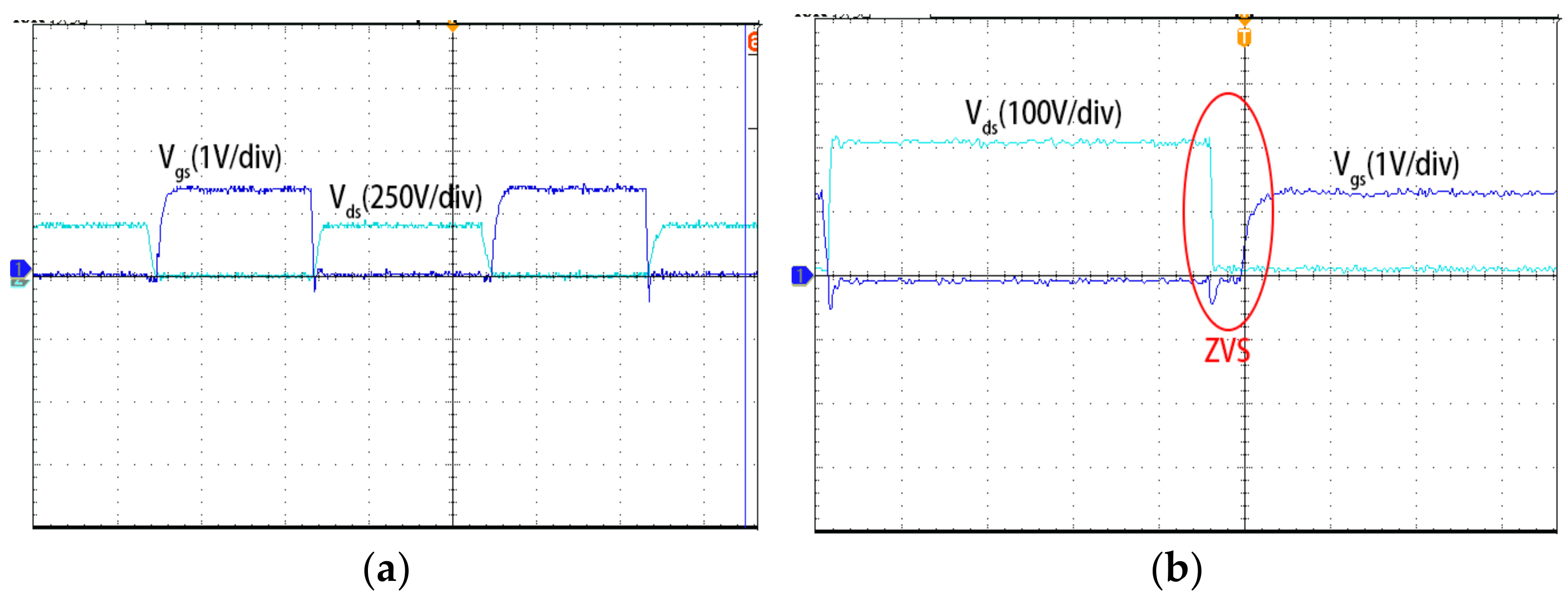
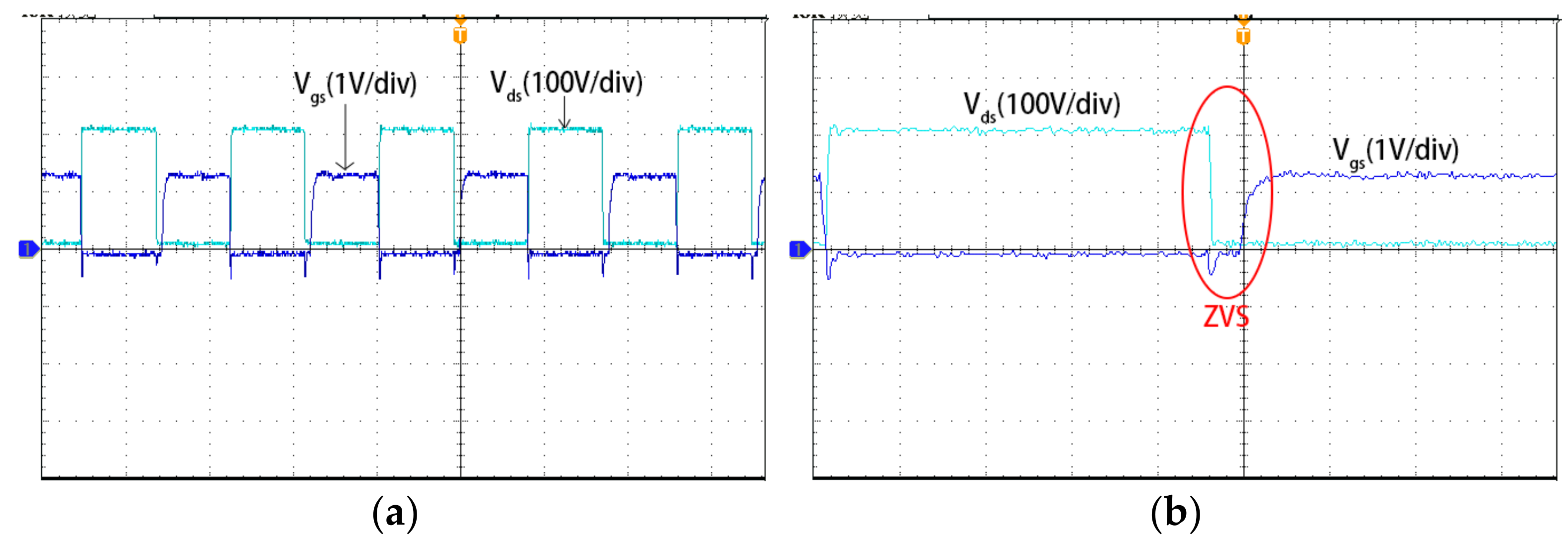
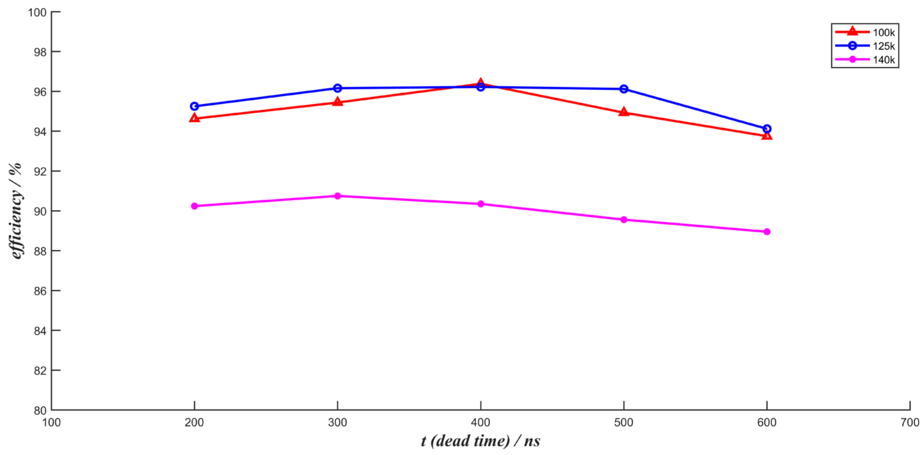
4.2. Analysis of Experimental Results

Experiments are performed separately according to the dead time in Table 3. Firstly, the input voltage of the prototype is set to 200 V, and then the frequency and the corresponding dead time are changed sequentially. However, according to the results of the simulation experiment in Figure 6, Figure 7 and Figure 8, it is known that the dead time set by the method in [11] is too small, and there is a large overlap area between voltage and current when the semiconductor is on, so the turn-on loss is large. Additionally, there is still a large current spike at the turn-on instant, suggesting that the dead time setting is too short and does not achieve soft switching in its fullest sense, and it is possible for the upper and lower semiconductors of the same bridge arm to turn on simultaneously. The dead time required for the experimental prototype will only be longer than that required for the simulation, so from a safety point of view, the dead time calculated in [11] should not be used for experiments on the experimental prototype, otherwise it is prone to the danger of short circuit.
The results of the prototype experiment are shown in Figure 9, Figure 10 and Figure 11, which are derived from the oscilloscope. According to Figure 9, when the switching frequency is 100 kHz, there is still a very small overlap between the drive signal and the drain-source voltage, which results in some turn-on loss. However, due to the very short overlap time, the current rises very slowly during this time, which can be approximated as the realization of ZVS. The above analysis shows that when the converter works at fs < fr, the dead time calculated by using the method in this paper is small, so when the converter works at under-resonant operation, the calculated dead time can be increased appropriately, and a certain margin can be added to ensure the complete realization of ZVS. As obtained from Figure 10 and Figure 11, the converter operates in the range of fsfr, and the drain-source voltages have all dropped to zero when the drive signal comes, thus fully achieving ZVS and verifying the correctness of the method in this paper. According to Figure 10, the drive signal arrives just in time when the drain-source voltage drops to zero, so that minimum switch loss is maintained while the ZVS is achieved.
The size of the dead time is a compromise between the switching losses and the overall efficiency of the converter. As can be seen in Figure 12, the converter efficiency increases or remains almost constant with increasing dead time when the dead time is less than 400 ns. If the dead time exceeds 400 ns, the loss of duty cycle caused by the excessive dead time leads to a reduction in output power, causing the converter’s efficiency to decrease.
However, Figure 12 shows that the actual resonant frequency of the prototype deviates from the theoretical calculation, so that the maximum efficiency of the converter is not at the calculated resonant frequency. From Table 4, it can be seen that the maximum efficiency of the designed experimental prototype is about 93%, while the maximum efficiency of this paper is about 96%. The design of all the parameters in this paper is the same as that in [11], except for the dead time. Therefore, the dead time design method proposed in this paper is beneficial to improving the overall efficiency of the converter. Moreover, the margin α can also be adjusted to make the efficiency reach the optimal value according to actual circuit conditions, which has the advantages of flexibility and practicality.

5. Conclusions

With the rapid development of third-generation semiconductors, SiC semiconductors are also being applied to LLC resonant converters. It is necessary to research the characteristics of SiC semiconductors, especially the dead time, which plays a crucial role in the realization of ZVS. In this paper, we analyze the process and necessary conditions for soft switching of a full-bridge LLC resonant converter and establish the equivalent circuit model of the converter using FHA. According to the analysis of the soft switching implementation process, the actual dead time of a full-bridge LLC resonant converter is not only determined by the parasitic capacitors charging and discharging times, but also by the delay in conduction of the semiconductors, the delay in conduction of the body diodes, and the error caused by FHA. At the same time, due to problems like the printed circuit board, there is usually some interference in the actual circuit, such as stray inductance and stray capacitance, so a certain margin needs to be considered when designing the dead time. The dead time has a definite effect on the switching losses and has an important influence on the efficiency of converters. Too large or too small a dead time can lead to a reduction in efficiency. Thus, there is a great deal of importance for the converter to have an accurate and suitable dead time. In this paper, a new method of dead time calculation is proposed that can reduce computation time and improve the efficiency of the system. However, when analyzing the influence of the driver circuit on the dead time, the driver circuit is not modeled precisely, but the method of adding margin is adopted. This method is applicable to all LLC resonant converters but gives up some accuracy. Later on, a generalized method can be derived based on the accurate modeling of the drive circuit, thus further improving the accuracy of the dead time.

Author Contributions

Conceptualization, L.W. and W.L.; methodology, L.W. and W.L.; software, L.W.; validation, L.W.; formal analysis, L.W.; investigation, L.W.; data curation, L.W.; writing—original draft preparation, L.W.; writing—review and editing, L.W., W.L., Y.W. and H.L.; supervision, W.L., Y.W. and H.L. All authors have read and agreed to the published version of the manuscript.

Funding

This work was funded by the National Natural Science Foundation of China (No. 61563006).

Conflicts of Interest

The authors declare no conflict of interest.

References

  1. Wu, Y.-E.; Wang, J.-W. Novel High-Efficiency High Step-Up DC–DC Converter with Soft Switching and Low Component Voltage Stress for Photovoltaic System. Processes 2021, 9, 1112. [Google Scholar] [CrossRef]
  2. Lin, B.-R. Analysis of a Series-Parallel Resonant Converter for DC Microgrid Applications. Processes 2021, 9, 542. [Google Scholar] [CrossRef]
  3. Ta, L.A.D.; Dao, N.D.; Lee, D.-C. High-Efficiency Hybrid LLC Resonant Converter for On-Board Chargers of Plug-In Electric Vehicles. IEEE Trans. Power Electron. 2020, 35, 8324–8334. [Google Scholar] [CrossRef]
  4. Fei, C.; Gadelrab, R.; Li, Q.; Lee, F.C. High-Frequency Three-Phase Interleaved LLC Resonant Converter with GaN Devices and Integrated Planar Magnetics. IEEE J. Emerg. Sel. Top. Power Electron. 2019, 7, 653–663. [Google Scholar] [CrossRef]
  5. Lin, H.; Jin, X.; Xie, L.; Hu, J.; Lu, Z. A New Variable-Mode Control Strategy for LLC Resonant Converters Operating in a Wide Input Voltage Range. J. Zhejiang Univ. Sci. C 2017, 18, 410–422. [Google Scholar] [CrossRef]
  6. Menke, M.F.; Duranti, J.P.; Roggia, L.; Bisogno, F.E.; Tambara, R.V.; Seidel, Á.R. Analysis and Design of the LLC LED Driver Based on State-Space Representation Direct Time-Domain Solution. IEEE Trans. Power Electron. 2020, 35, 12686–12701. [Google Scholar] [CrossRef]
  7. Feng, X. LLC Resonant Converter Loss Analysis and Efficiency Optimization; Beijing Jiaotong University: Beijing, China, 2017. [Google Scholar]
  8. Gao, T.; Cheng, Z.; Wang, Q.; Li, Y.; Zeng, K.; Yang, Y. The Analysis of Dead Time’s Influence on the Operating Characteristics of LLC Resonant Converter. In Proceedings of the 2019 14th IEEE Conference on Industrial Electronics and Applications (ICIEA), Xi’an, China, 19–21 June 2019; pp. 85–89. [Google Scholar]
  9. Lee, I.-O.; Moon, G.-W. Analysis and Design of a Three-Level LLC Series Resonant Converter for High- and Wide-Input-Voltage Applications. IEEE Trans. Power Electron. 2012, 27, 2966–2979. [Google Scholar] [CrossRef]
  10. Deng, J.; Li, S.; Hu, S.; Mi, C.C.; Ma, R. Design Methodology of LLC Resonant Converters for Electric Vehicle Battery Chargers. IEEE Trans. Veh. Technol. 2014, 63, 1581–1592. [Google Scholar] [CrossRef]
  11. Huang, H. Designing an LLC Resonant Half-Bridge Power Converter. In 2010 Texas Instruments Power Supply Design Seminar, SEM1900, Topic; Texas Instruments Incorporated: Dallas, TX, USA, 2010; Volume 3, pp. 2010–2011. [Google Scholar]
  12. Beiranvand, R.; Rashidian, B.; Zolghadri, M.R.; Alavi, S.M.H. Optimizing the Normalized Dead-Time and Maximum Switching Frequency of a Wide-Adjustable-Range LLC Resonant Converter. IEEE Trans. Power Electron. 2011, 26, 462–472. [Google Scholar] [CrossRef]
  13. Lü, Z.; Yan, X.; Sun, I.; Fan, W. Selection and calculation of dead time for LLC converters taking into account MOSFET turn-off process. Electr. Power Autom. Equip. 2017, 37, 175–183. [Google Scholar] [CrossRef]
  14. Sun, Y.; Deng, Z.; Xu, G.; Deng, G.; Ouyang, Q.; Su, M. ZVS Analysis and Design for Half Bridge Bidirectional LLC-DCX Converter with Consideration of Nonlinear Capacitance and Different Load Under Synchronous Turn-On and Turn-Off Modulation. IEEE Trans. Transp. Electrif. 2022, 8, 2429–2443. [Google Scholar] [CrossRef]
  15. Han, D.; Sarlioglu, B. Comprehensive Study of the Performance of SiC MOSFET-Based Automotive DC–DC Converter under the Influence of Parasitic Inductance. IEEE Trans. Ind. Appl. 2016, 52, 5100–5111. [Google Scholar] [CrossRef]
  16. Vechalapu, K.; Bhattacharya, S.; Van Brunt, E.; Ryu, S.-H.; Grider, D.; Palmour, J.W. Comparative Evaluation of 15-KV SiC MOSFET and 15-KV SiC IGBT for Medium-Voltage Converter Under the Same Dv/Dt Conditions. IEEE J. Emerg. Sel. Top. Power Electron. 2017, 5, 469–489. [Google Scholar] [CrossRef]
  17. Li, Z.; Wang, J.; Ji, B.; Shen, Z.J. Power Loss Model and Device Sizing Optimization of Si/SiC Hybrid Switches. IEEE Trans. Power Electron. 2020, 35, 8512–8523. [Google Scholar] [CrossRef]
  18. Akagi, H.; Kinouchi, S.; Miyazaki, Y. Bidirectional Isolated Dual-Active-Bridge (DAB) DC-DC Converters Using 1.2-KV 400-A SiC-MOSFET Dual Modules. CPSS Trans. Power Electron. Appl. 2016, 1, 33–40. [Google Scholar] [CrossRef]
  19. Costa, L.F.; Buticchi, G.; Liserre, M. Highly Efficient and Reliable SiC-Based DC–DC Converter for Smart Transformer. IEEE Trans. Ind. Electron. 2017, 64, 8383–8392. [Google Scholar] [CrossRef] [Green Version]
  20. Hazra, S.; De, A.; Cheng, L.; Palmour, J.; Schupbach, M.; Hull, B.A.; Allen, S.; Bhattacharya, S. High Switching Performance of 1700-V, 50-A SiC Power MOSFET Over Si IGBT/BiMOSFET for Advanced Power Conversion Applications. IEEE Trans. Power Electron. 2016, 31, 4742–4754. [Google Scholar] [CrossRef]
  21. Karimi, S.; Tahami, F. A Comprehensive Time-Domain-Based Optimization of a High-Frequency LLC-Based Li-Ion Battery Charger. In Proceedings of the 2019 10th International Power Electronics, Drive Systems and Technologies Conference (PEDSTC), Shiraz, Iran, 12–14 February 2019; pp. 415–420. [Google Scholar]
  22. Sun, C.; Sun, Q.; Wang, R.; Li, Y.; Ma, D. Adaptive Dead-Time Modulation Scheme for a Bidirectional LLC Resonant Converter in Energy Router. CSEE J. Power Energy Syst. 2021, 5, 1–10. [Google Scholar] [CrossRef]
  23. Huang, J.; Zhao, Z.; Han, P. Research on Dead Time of Half-Bridge LLC Resonant Circuit Based on SiC MOSFET. In Proceedings of the 2021 IEEE 16th Conference on Industrial Electronics and Applications (ICIEA), Chengdu, China, 1–4 August 2021; pp. 855–860. [Google Scholar]
  24. Murakami, Y.; Sato, T.; Nishijima, K.; Nabeshima, T. Small Signal Analysis of LLC Current Resonant Converters Using Equivalent Source Model. In Proceedings of the IECON 2016—42nd Annual Conference of the IEEE Industrial Electronics Society, Florence, Italy, 24–27 October 2016; pp. 1417–1422. [Google Scholar]
  25. Sun, W.; Xing, Y.; Wu, H.; Ding, J. Modified High-Efficiency LLC Converters with Two Split Resonant Branches for Wide Input-Voltage Range Applications. IEEE Trans. Power Electron. 2018, 33, 7867–7879. [Google Scholar] [CrossRef]
  26. Yao, X.; Jin, X.; Zhou, F. Effect of diode reverse recovery in zero-voltage, zero-current conversion soft-switching technology. Proc. CSEE 2015, 35, 944–952. [Google Scholar] [CrossRef]
  27. Luo, Y.; Xiao, F.; Tang, Y. Study on the mechanism of the reverse recovery voltage spike of the renewal transient of a current-continuing diode. Acta Phys. Sin. 2014, 63, 333–341. [Google Scholar] [CrossRef]
Figure 1. The topology of the full-bridge LLC resonant converter.
Processes 11 00973 g001
Figure 2. The working waveform of the full-bridge LLC resonant converter. (a) fm < fs < fr (b) fs = fr (c) fs > fr.
Processes 11 00973 g002aProcesses 11 00973 g002b
Figure 3. Equivalent circuit of the full-bridge LLC resonant converter.
Processes 11 00973 g003
Figure 4. The working waveform of the full-bridge LLC resonant converter.
Processes 11 00973 g004
Figure 5. Experimental prototype.
Processes 11 00973 g005
Figure 6. Simulation results for fs = 100 kHz: (a) Steady-state waveforms (time scale: 4 µs/div); (b) partial amplification waveforms (time scale: 800 ns/div).
Processes 11 00973 g006
Figure 7. Simulation results for fs = 125 kHz: (a) Steady-state waveforms (time scale: 4 µs/div); (b) partial amplification waveforms (time scale: 800 ns/div).
Processes 11 00973 g007
Figure 8. Simulation results for fs = 140 kHz: (a) Steady-state waveforms (time scale: 4 µs/div); (b) partial amplification waveforms (time scale: 800 ns/div).
Processes 11 00973 g008
Figure 9. Experimental results for fs = 100 kHz: (a) Steady-state waveforms (time scale: 4 µs/div); (b) Soft-switching waveforms (time scale: 800 ns/div).
Processes 11 00973 g009
Figure 10. Experimental results for fs = 125 kHz: (a) Steady-state waveforms (time scale: 2 µs/div); (b) Soft-switching waveforms (time scale: 800 ns/div).
Processes 11 00973 g010
Figure 11. Experimental results for fs = 140 kHz: (a) Steady-state waveforms (time scale: 4 µs/div); (b) Soft-switching waveforms (time scale: 800 ns/div).
Processes 11 00973 g011
Figure 12. The relation curve between dead-time and efficiency.
Processes 11 00973 g012
Table 1. Specifications of the converter.
ParameterSymbolValue
range of input voltages (V)Vin180–300
rated input voltage (V)Vin-nom200
rated output voltage (V)Vout-nom170
frequency of resonance (kHz)fr125
the power of the output (kW)Po2
Table 2. Design parameters for converter.
ComponentSymbolValue
SiC semiconductorS1~S4CI60N120SM
Transformer (ratio)n1.16
magnetizing inductance (µH)Lm65
resonant inductor (µH)Lr16.53
resonant capacitor (nF)Cr100
filter capacitor of the primary side (µF)Cin19.4
filter capacitor of the secondary side (µF)Cout22.2
Table 3. Calculation results of dead time under different methods.
Switching Frequency (kHz)100125140
the dead time calculated by the proposed method (ns)293.37308.95318.26
the dead time calculated by the method in [11] (ns)≥18.9≥23.62≥26.45
Table 4. The proposed method compared with the other paper.
Description[11]Proposed
Resonant frequency135 kHz125 kHz
Dead timeFixedAdaptive
Maximum efficiency93%96.1%
Disclaimer/Publisher’s Note: The statements, opinions and data contained in all publications are solely those of the individual author(s) and contributor(s) and not of MDPI and/or the editor(s). MDPI and/or the editor(s) disclaim responsibility for any injury to people or property resulting from any ideas, methods, instructions or products referred to in the content.

