
Modeling and Simulation of a TFET-Based Label-Free Biosensor with Enhanced Sensitivity
by
 , , and
Sagarika Choudhury
1,*,
Krishna Lal Baishnab
1,
Koushik Guha
1,
Zoran Jakšić
2 ,
,
Olga Jakšić
2 and
and
Jacopo Iannacci
3,*
1
Department of Electronics and Communication Engineering, National Institute of Technology, Silchar 788010, India
2
Center of Microelectronic Technologies, Institute of Chemistry, Technology and Metallurgy, National Institute of the Republic of Serbia, University of Belgrade, 11000 Belgrade, Serbia
3
Center for Sensors and Devices (SD), Fondazione Bruno Kessler (FBK), 38123 Trento, Italy
*
Authors to whom correspondence should be addressed.
Chemosensors 2023, 11(5), 312; https://doi.org/10.3390/chemosensors11050312
Submission received: 18 March 2023
/
Revised: 18 May 2023
/
Accepted: 21 May 2023
/
Published: 22 May 2023
(This article belongs to the Special Issue State-of-the-Art (Bio)chemical Sensors—Celebrating 10th Anniversary)
Abstract
:This study discusses the use of a triple material gate (TMG) junctionless tunnel field-effect transistor (JLTFET) as a biosensor to identify different protein molecules. Among the plethora of existing types of biosensors, FET/TFET-based devices are fully compatible with conventional integrated circuits. JLTFETs are preferred over TFETs and JLFETs because of their ease of fabrication and superior biosensing performance. Biomolecules are trapped by cavities etched across the gates. An analytical mathematical model of a TMG asymmetrical hetero-dielectric JLTFET biosensor is derived here for the first time. The TCAD simulator is used to examine the performance of a dielectrically modulated label-free biosensor. The voltage and current sensitivity of the device and the effects of the cavity size, bioanalyte electric charge, fill factor, and location on the performance of the biosensor are also investigated. The relative current sensitivity of the biosensor is found to be about 1013. Besides showing an enhanced sensitivity compared with other FET- and TFET-based biosensors, the device proves itself convenient for low-power applications, thus opening up numerous directions for future research and applications.
1. Introduction
The need for effective biosensors has increased greatly in recent times owing to the COVID-19 pandemic. Although a vast number of different biosensors have been designed to sense analytes such as proteins, toxins, DNA, viruses, bacteria, other pathogens, etc. [1,2,3], most of these are based on complex techniques that increase the cost as well as the detection time [4,5]. The innumerable existing types of biosensors can be classified based on their transduction mechanisms. Among the sensors widely used today are electrochemical ones [6,7] (genic, etc.), electronic biosensors (typically including variants of FET transistors, e.g., ordinary FET, MOSFET, ISFET, TFET, etc.), and gravimetric ones (thermal, acoustic, etc.) [8,9,10,11,12]. All of the quoted sensor classes have their own sets of advantages and disadvantages, but the most convenient biosensor is hard to find and would depend on a specific application.
Among the quoted devices, electronic biosensors have the advantage of mature fabrication technologies (the family of planar technologies) and their compatibility and integrability with standard silicon-integrated circuits. Our further attention here is dedicated to this class of biosensors.
Many of the existing biosensors suffer from false positives. While designing such devices, one must consider factors such as accuracy, speed, and cost. In solving these issues for electronic biosensors, dielectric modulation (DM)-based sensors [13] have gained importance, with either label-free [14] or labeled detection techniques. The former makes use of physical parameters such as relative dielectric permittivity to detect the presence of biomolecules, while the latter usually involves a chemical-binding reaction with a receptor. Label-free techniques are preferred as they involve direct detection and are fast, and the sensors based on them are typically reusable. TFET-based biosensors [15,16,17,18,19] that operate on the principle of tunneling with a subthreshold swing (SS) below 60 mV/dec are preferred. In addition, the FET-based biosensors proposed in references [3,4,5] are much more advantageous owing to their high sensitivity and cost-effectiveness.
A biosensor based on dielectric modulation was designed using a double gate (DG) FET by Narang et al. [20]. This work achieved a relative current sensitivity (defined as the ratio of ON and OFF currents) of 1010 for dielectric permittivity values 1–12. A relative current sensitivity of 107 was reported by Shafi et al. in a virtually doped TFET biosensor [21]. Further, a dopingless TFET biosensor with a current ratio of 1010 was described by Anand et al. [22]. A mathematical model for the TFET-based biosensor was presented by Rakhi et al. [23]. An analytical model for a split gate TFET biosensor was proposed by Singh et al. [24].
Because of their inherent operating principle, FET-based biosensors [13,15] suffer from high subthreshold swing (SS) and short-channel effects (SCE). However, in a TFET, it is quite difficult to realize abrupt junctions [25], which are essential for tunneling. Thus, JLTFETs come into the picture. These are basically an amalgamation of two concepts: a JLFET and the tunneling phenomenon. The JLTFET operation is based on the theory of work function modulation [25], where a uniformly doped n-type device with no initial potential barrier is made to behave as a PIN structure. Thus, the process of physical doping is avoided in JLTFETs, and the junctions are created by metal electrodes. Further, a JLTFET incorporates two gates: a polar gate at zero bias for inducing the P+ region with a high work function metal and a control gate for inducing the channel region by varying the work function. During the OFF state, because of the work function difference, the channel is depleted, and a barrier is created; hence, tunneling is negligible. As suitable gate bias is applied, the electron concentration below the control gate increases, the region becomes n-type, the barrier narrows, the channel is aligned, and tunneling takes place. Thus, the fabrication complexity of a conventional TFET and random dopant fluctuations are avoided in a JLTFET. Hence, JLTFET-based biosensors that have the advantages of TFETs and uniform doping are found to provide much better results than the other types of FET-based sensors. JLTFETs are much easier to fabricate, less prone to short-channel effects (SCE), and have an SS below 60. Chakraborty et al. [26] proposed the a for a surrounding gate JLTFET biosensor operated using the dielectric modulation technique. Gao [27] proposed an ultrasensitive biosensor for point-of-care diagnostics.
Most of the biosensors proposed in the literature suffer from low sensitivity, and realizing abrupt junctions with TFETs is difficult. This work presents a technique to improve the sensitivity of the existing biosensors by using a triple material gate (TMG) asymmetrical hetero-dielectric (AHD) junctionless tunnel field-effect transistor (JLTFET); i.e., it describes a TMG-AHD-JLTFET-based biosensor. Moreover, this work also derives an analytical mathematical model and validates the simulated results. The goal of this research is to determine the highest sensitivity of the proposed device when examining neutral and charged biological molecules. In addition, the impacts of various values of a biomolecule’s relative permittivity on the drain current, subthreshold slope, current ratio, and their sensitivity for both neutral and charged biological molecules are investigated.
The paper is organized as follows. First, the design of the device used as a biosensor is described, and then, the workings and development of the mathematical model and simulation procedure are discussed. The paper continues with the analysis of the obtained results. General conclusions are drawn at the end.
2. Materials and Methods
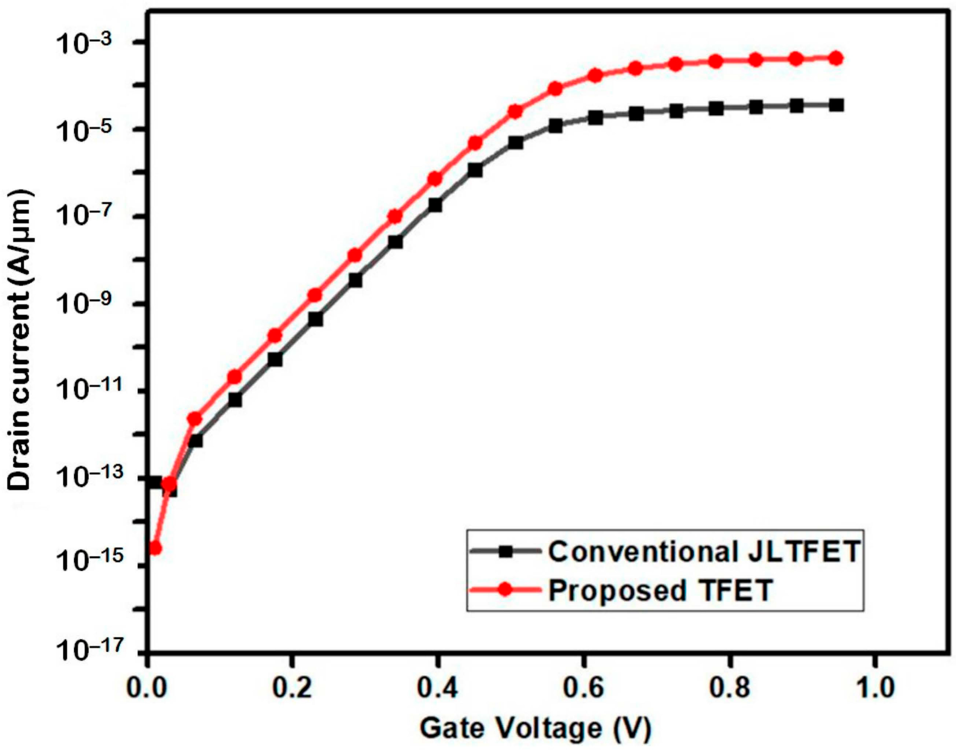
The biosensor in this work is designed as a junctionless device with an asymmetrical hetero-dielectric and triple material [28,29,30,31] control gate. The biosensor cross-section is shown in Figure 1. The dielectric layer consists of two strata of different materials. High-k and low-k dielectric materials are combined in the top gate dielectric’s initial layer, which is followed by a high-k layer. Here, k denotes relative dielectric permittivity. The lower gate, however, only has one high-k layer of 2 nm thick. In addition, a 2 nm spacer is added between the gates for improved isolation. In addition, a triple material gate (TMG) [28,29,30,31], where M1 is aluminum, M2 is cobalt, and M3 is scandium, has the benefit of enhanced gate control and greater carrier mobility, combined with asymmetry in the dielectric for improved performance. The use of high-permittivity material close to the tunneling junction enhances the electric field across the junction, which, in turn, improves the tunneling efficiency and increases the ON current. Similarly to this, using low-k material close to the drain causes the OFF current to drop. Consequently, it has been found that using TMGs with asymmetric hetero-dielectrics considerably improves the current ratio with moderate SS levels. The suggested device is calibrated with a traditional JLTFET [25], as depicted in Figure 2.
The basic operation of the proposed biosensor can be explained by the phenomenon of dielectric modulation [31,32,33,34,35], wherein the change in dielectric material across the cavity enhances the effective coupling across the tunnel junction. This, in turn, changes the overall surface potential and thereby affects the electric field across the tunneling area, which results in an increased output current. The dielectric of the control gate is etched to form a cavity that serves as the entrapment surface of the biosensor. A basic 2 nm layer dielectric is kept intact for isolation purposes, and then, the cavity is etched. The process of etching is similar to the one described in [36].
A list of various parameters for designing the biosensor is presented in Table 1. It is preferred to etch the cavity at the tunnel junction for better impact and control.
The simulations were performed using the Synopsis TCAD tool [37], and a non-local band was incorporated into the band-tunneling model [38]. The nonlocal model defines the electric field for each mesh and proves to be more accurate. As the device is highly doped, the band-gap-narrowing model is enabled; the Shockley–Read–Hall (SRH) model is included to study the impact of high impurity and interface trap charges; and the trap-assisted tunneling (TAT) model is also included to incorporate the impact of band-to-band tunneling (BTBT) and interface traps. Thus, at the biosensor’s sensing part, a nano-gap is created in the dielectric layer near the source region. A portion is etched using photolithography to create the gap. Thereafter, the source and the drain are created by depositing gate materials with a suitable work function. This is a purely simulation-based approach.
3. Analytical Model of Device as Biosensor
The potential distribution is represented by Poisson’s equation as [31]
where denotes the channel doping, is silicon dielectric permittivity, L is the control gate length, denotes the channel potential, q is the elementary electron charge, and is the thickness of the device. represents the surface potential and are coefficients and functions of the position on the surface [16].
The surface potential of different metals is represented as
Here, j = 1, 2, 3 for metals M1, M2, M3, respectively; for and 0 , represents potential. The channel starts at L0, and the length of the cavity is Lc = L2 + L3. The use of three gate materials marks the presence of different flat band voltages and work functions. denotes the electron affinity, is a band gap at 300 K, and is the Fermi potential [30].
where represent the work functions of different metals, and is the silicon work function [19,31].
where is thermal voltage while represents the intrinsic concentration of silicon. Considering the continuity of the electric field along the front and back gate, we can write [31]
The capacitance below metal M1 () is the combination of the capacitance across the basic dielectric layer () and the fixed oxide capacitance () [29]
where
Coxbasef 1 = capacitance of basic dielectric layer. Cofixed = capacitance of SiO2 layer near the cavity.
Again, for metal gate M2, the capacitance of the basic dielectric layer (Coxbasef 2) is represented as
where
Similarly, the basic dielectric layer capacitance across M3 () is
where toxf is the thickness of the front oxide, while and are the dielectric permittivities of HfO2 and SiO2.
As shown in Figure 1, the cavity is formed under metal gates M2 and M3. The biomolecules are trapped under layers M2 and M3, and this changes the capacitance below M2 and M3.
For the cavity where biomolecules are trapped, .
For a partially filled nano-gap under M2 and M3,
where and .
Similarly, the basic dielectric layer is fixed, hence,
is the back-gate potential. Thus, for a fully filled nano-gap in the back gate,
For j = 1, M1 is
For a partially filled nano gap under M2 and M3 in the back gate [16]
is the back gate potential for different metals (j = 1, 2, 3). + for M1, M2, and M3 [30]. is the surface potential.
The electric field continuity at the interface in the lateral direction is
where represents the built-in potential, and represents the voltage across the drain with respect to the source.
as the device is homogeneously doped [26]
The constants can be evaluated by solving Equation (3). The obtained values are written as
Substituting the above values into Equation (3) and comparing the result with Equation (1), we obtain
where
The surface potentials under the three regions are provided below:
where
To determine the boundary condition constants, Equation (6) is used:
The expression for the lateral electric field is derived as
The vertical electric field is
The expression for the current is obtained using Kane’s model [2,24] as
E is the average electric field, and is the energy bandgap.
Thus, the modeling of the TFET design can be initiated with the basic Poisson equation; then, the standard solution is represented by Equation (2). Depending on the device architecture, the materials used can be modified and represented in the equations. Finally, the surface potential and electric fields are computed and a continuity relation is applied. Once we obtain the electric field, we can also compute the drain current using Kane’s relation.
In a TFET-based biosensor, the main architecture change occurs only in the cavity region, which impacts the capacitance calculation. Thus, the capacitance in each region needs to be calculated.
4. Results and Discussions
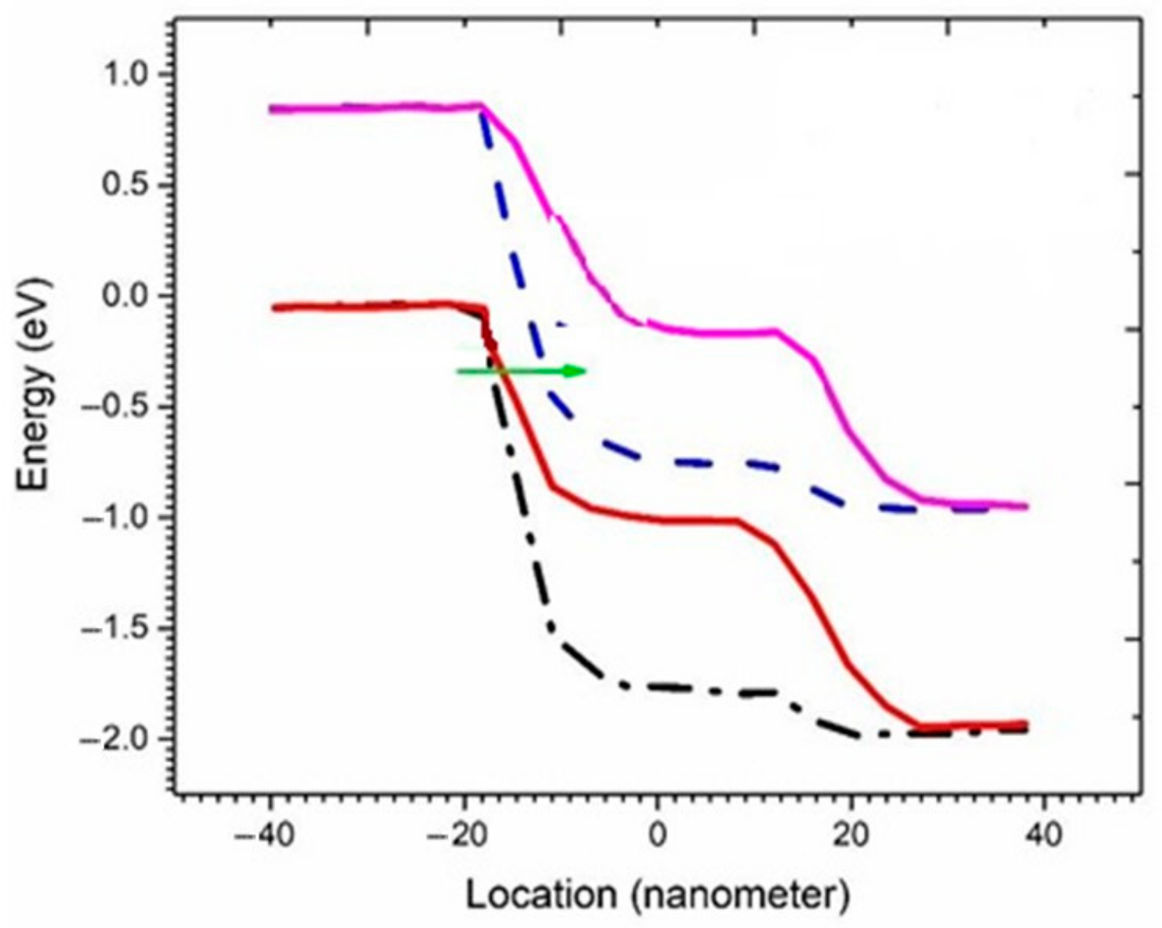
The energy band of the proposed biosensor is shown in Figure 3. As the dielectric permittivity across the cavity increases, the electric field maximizes, and, therefore, the best possible alignment occurs. The dotted line shows the alignment when a dielectric with a permittivity of k = 12 fills the cavity, whereas the straight line shows the situation for k = 1 (air). It was observed that there is less alignment between the bands for a cavity filled with air. If the energy bands that are aligned are higher, the tunneling width decreases, and thus, the probability of carrier tunneling is better. The green arrow in the figure depicts the tunnel width.
4.1. Validation of the Proposed Structure and Its Mathematical Model
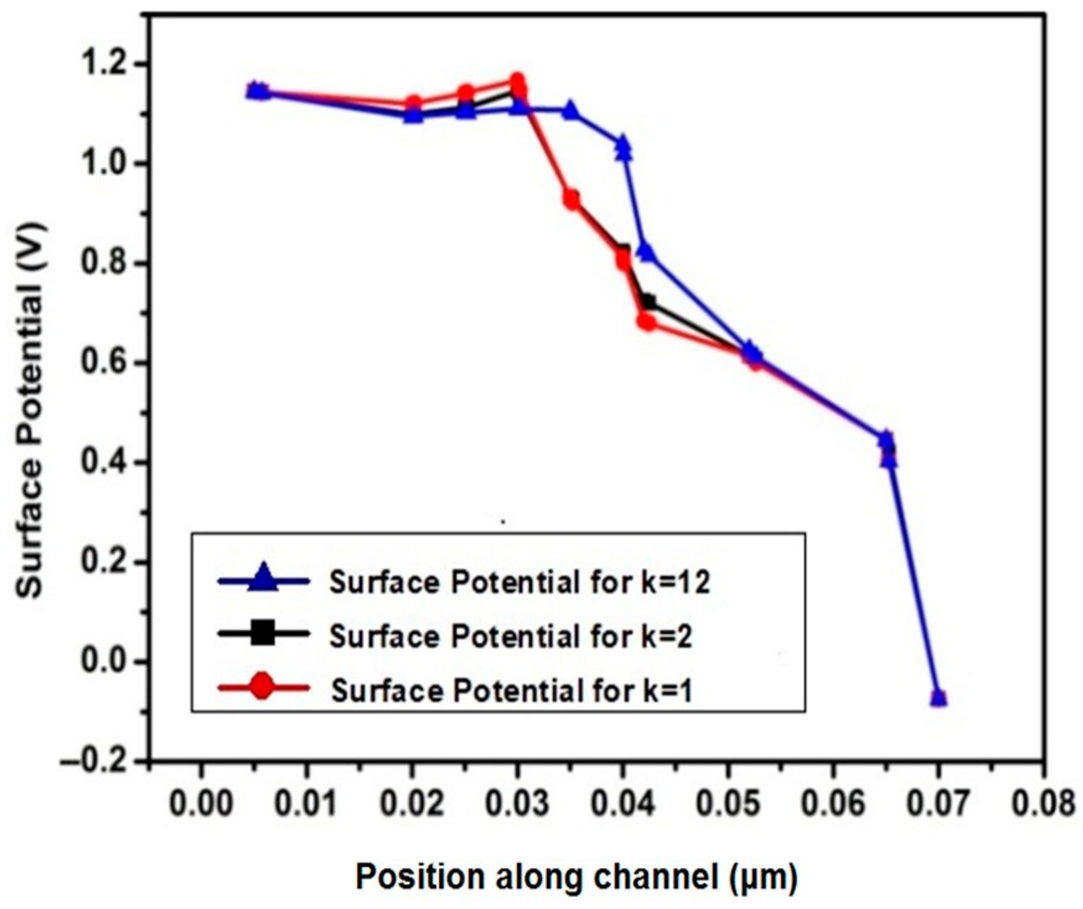
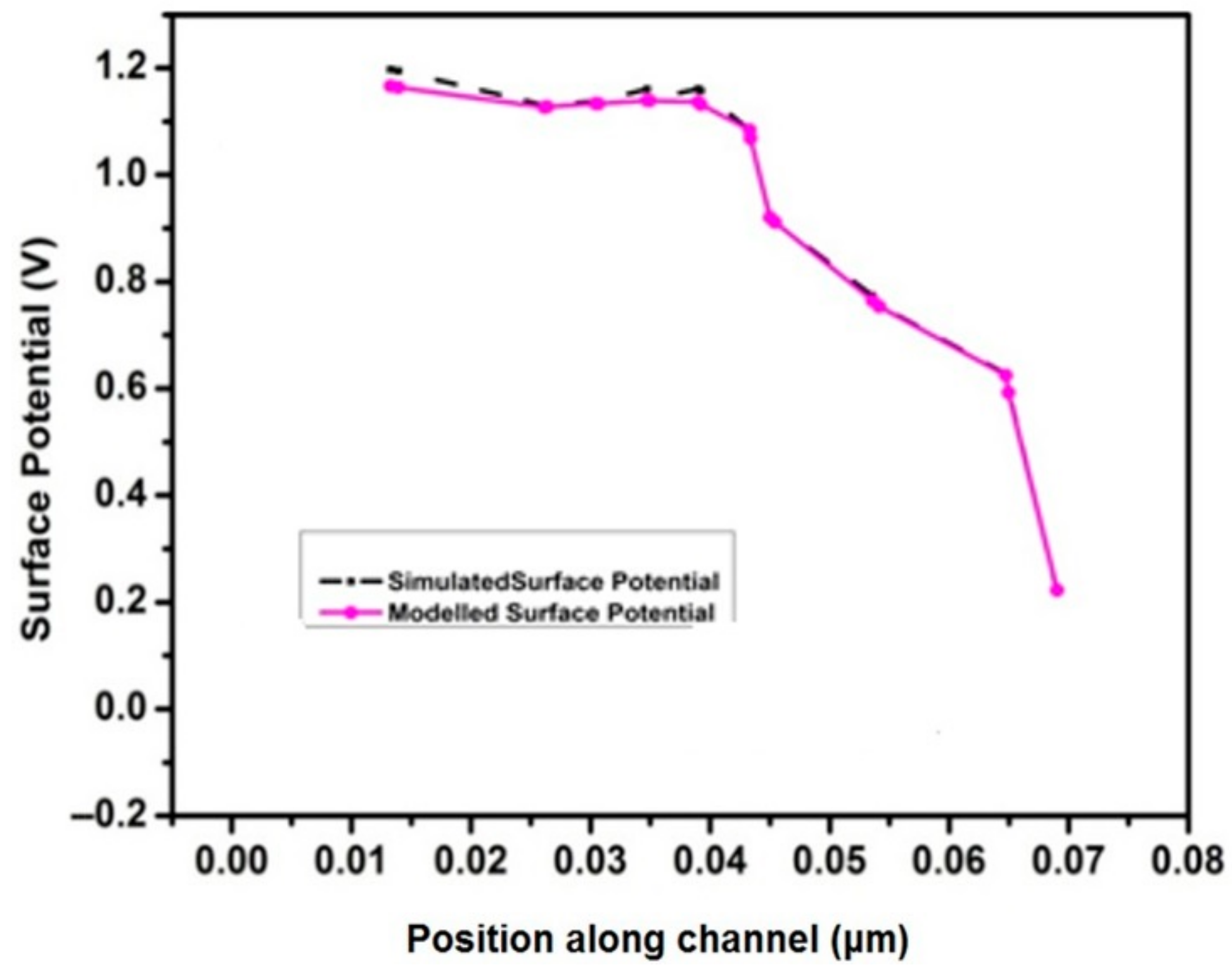
The performance of the proposed structure is validated by comparing it with the existing structures, as shown in Table 2. Similarly, the surface potential model is depicted in Figure 4 for various dielectrics. The variation in the potential along the channel is studied. It was observed that the potential drops across the channel. The step change in the potential profile is due to the use of three different materials across the control gate. The potential profile then drops to zero in the source region. Because of the higher effective capacitance caused by the increased dielectric permittivity, k, the barrier width at the source-channel junction drops, resulting in a rapid rise in the surface potential across the tunneling area. Thereafter, the modeled and simulated values of the surface potential are compared in Figure 5. The graph demonstrates the congruence of the surface potential values between those that were modeled and those that were simulated, thus proving the viability of the suggested model.
4.2. Drain Current Variation for Different Values of k for Electrically Neutral Biomolecules
The current variation for different dielectrics in fully filled nano-gaps is shown in Figure 6. The analyte materials selected are air (k = 1.0), biotin (k = 2.0), ferro-cytochrome (k = 4), bacteriophage T7 (k = 6), zein (k = 7), keratin (k = 9), and gelatin (k = 12), as shown in Table 3. The similarity between the analytically modeled and simulated values shows the accuracy of the proposed model. The gate oxide across the tunnel junction is etched to create biosensor cavities. Following that, analyte molecules with different dielectric permittivities, such as keratin, gelatin, etc., are filled into these cavities. Capacitances vary because of changes in the analyte dielectric permittivity. The ensuing change in capacitance causes a shift in the charge density across the junction, boosting the surface potential and, in turn, increasing the electric field across the junction. Thus, higher electric fields result in better coupling and thereby increase the current density, which is responsible for higher tunneling as the permittivity rises, and this results in a high current.
The selectivity of our sensor can be boosted in the usual way by functionalizing its sensing surface by attaching receptors to it that specifically bind the targeted analyte (ligand), thus vastly improving the affinity. Some of the convenient receptor–ligand pairs applied to a TFET with a source cavity are quoted in a paper by Soni et al. [40]. For the current sensor architecture, the specific binding occurs mainly via the cavity approach, wherein the dielectric modulation-based label-free sensing technique is used, thus ensuring the proper transduction of the amount of the targeted analyte to a proportional modification of the output electric signals. Consequently, a significant increase can be seen in the device surface potentials. This will result in a considerable increase in the charge carriers, which will intensify the abruptness across the junction. The capacitance will be impacted by this shift as well, which will alter the electric field, and thus, the drain current will also change.
This technique can also be used for measurements of a typical sample of dilute biomolecules in a solution. For biological applications, it is critical to correctly identify biomarkers in clinically pertinent samples. By injecting a solution into the cavity surface that does not contain the desired biomolecule (blank), a baseline for the device’s current can be established for a typical sample. When the solution containing the biomolecule is subsequently added, the device’s current changes right away and finally stabilizes. Ref. [27] described a similar method of dilute biomolecule detection.
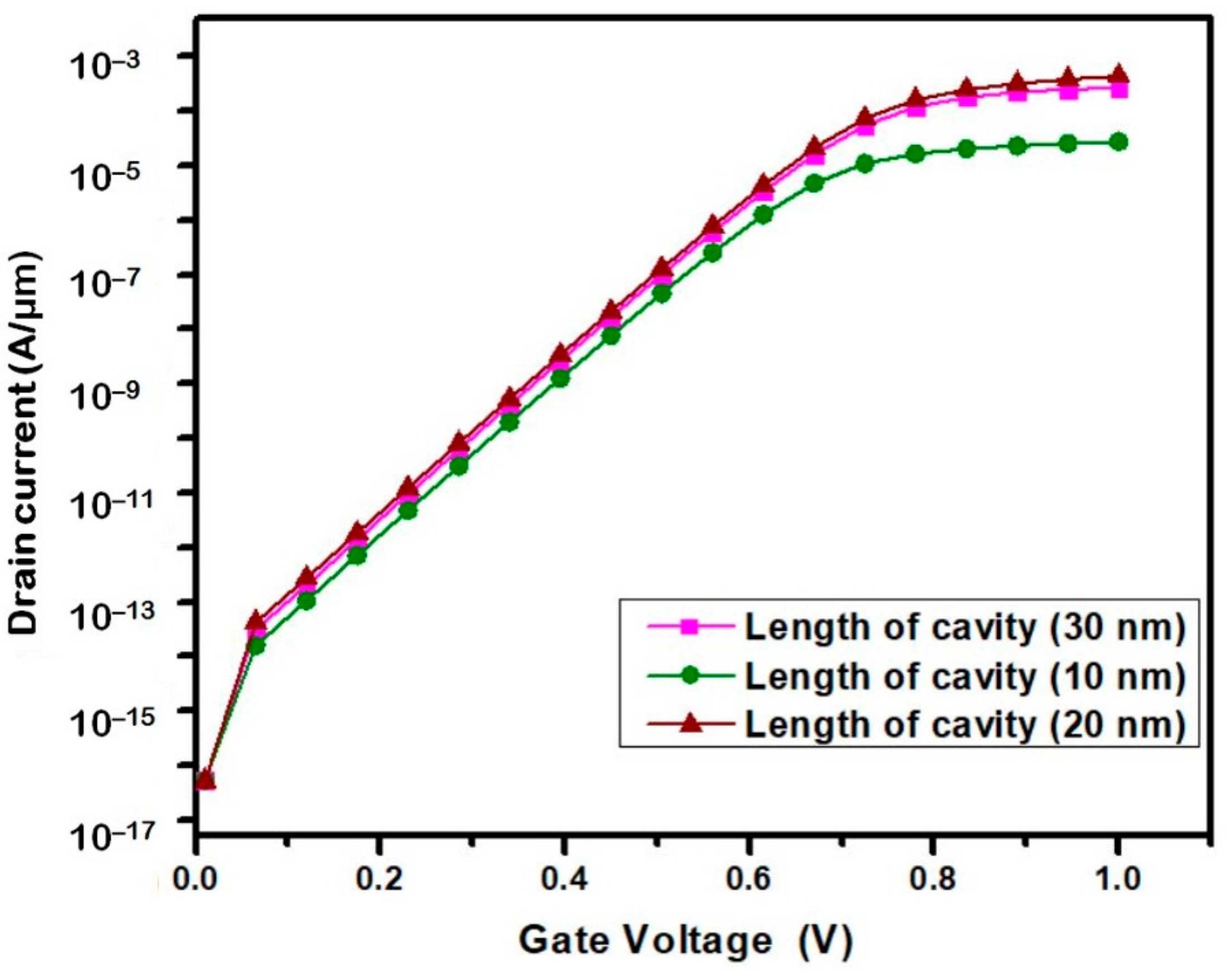
4.3. Effect of Variation of Drain Current with Length of Cavity
The cavity length varies from 10 nm to 30 nm, keeping k = 12 and the cavity thickness at 5 nm, while the gate voltage is maintained at 1 V and the drain voltage at 1 V. The drain current gate voltage dependence for different cavity lengths is shown in Figure 7. It was observed that, for a length of 10 nm, the current sensitivity is quite low, and if the length increases to 20 nm, the ON current raises. However, if we further increase the length, there is a small decrease in the drain current. Moreover, the OFF current remains almost constant. This behavior is due to the fact that, for a 20 nm cavity, the maximum electric field appears at the tunnel junction, and the energy bands are perfectly aligned. Thus, the maximum number of carriers can tunnel across the junction, resulting in an increase in the drain current. As we further increase the length, the alignment is impaired, and the tunneling reduces. The modeling and simulation results show similar values (overlapping in the figure).
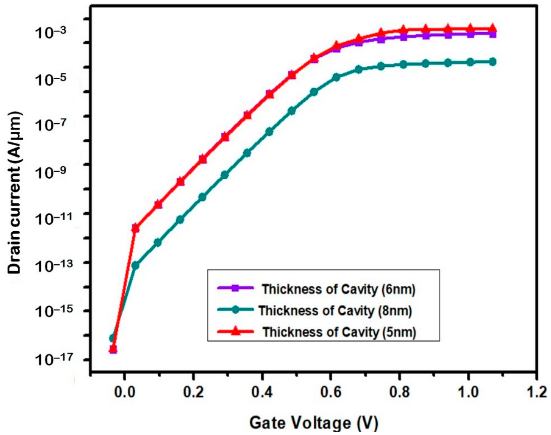
4.4. Effect of Drain Current Variation with Cavity Thickness
The impact of drain current variation on the thickness of the cavity is shown in Figure 8. The length of the cavity, the gate voltage, and the drain voltage are kept fixed at 20 nm, 1 V, and 1 V, respectively. It was found that, as the thickness increases, the effective tunneling barrier widens, and it becomes difficult for the carriers to tunnel across the junction. Therefore, as the carrier tunneling reduces, the drain current consequently decreases. Because of poor gate control in the channel area, the current drops as the thickness rises while the threshold voltage rises.
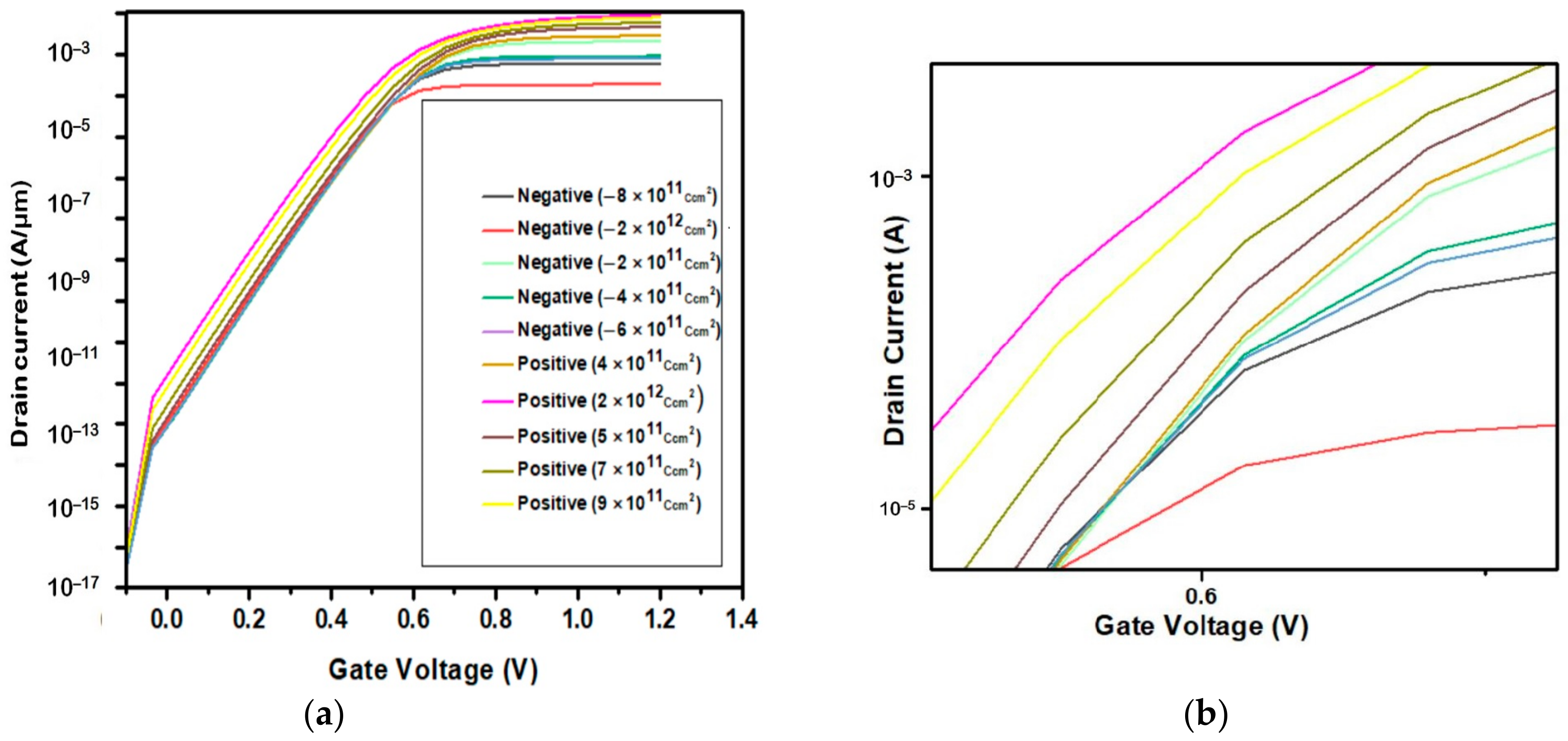
4.5. Effects of Electrically Charged Biomolecules
The impact of electrically charged (positive/negative) biomolecules in a fully filled nano-gap is depicted in Figure 9. The graph shows that the drain current rises with an increase in positive charges (a left shift of the characteristics), whereas it decreases with an increase in negative charges (a right shift). This can be represented by the MOSFET equation [32]:
where the symbols have their usual meaning.
The charge in a biomolecule significantly depends on pH. In our simplified model, proteins and nucleic acids, as charged macromolecules, are represented by the charges of their ionizable residues. The measurement of charges is carried out at a particular pH. Some experimental ranges for charges in biomolecules, as mentioned in [41], at pH 7 are shown here (a charge of 1.0 e for Arg and Lys; a charge of 1.0 e for Glu and Asp). As mentioned in [42], biotin has a pI of 3.5, where pI signifies the isoelectric point. The isoelectric point is the pH value where a molecule exhibits a neutral net charge. For any value below pI, the biomolecule exhibits a positive surface charge, and above that, it represents a negative surface charge. Similarly, streptavidin has a pI value of 5.5.
Conventionally, most of the reported TFET-based biosensors were tested for a charge range of −5 × 10¹¹ to +5 × 10¹².
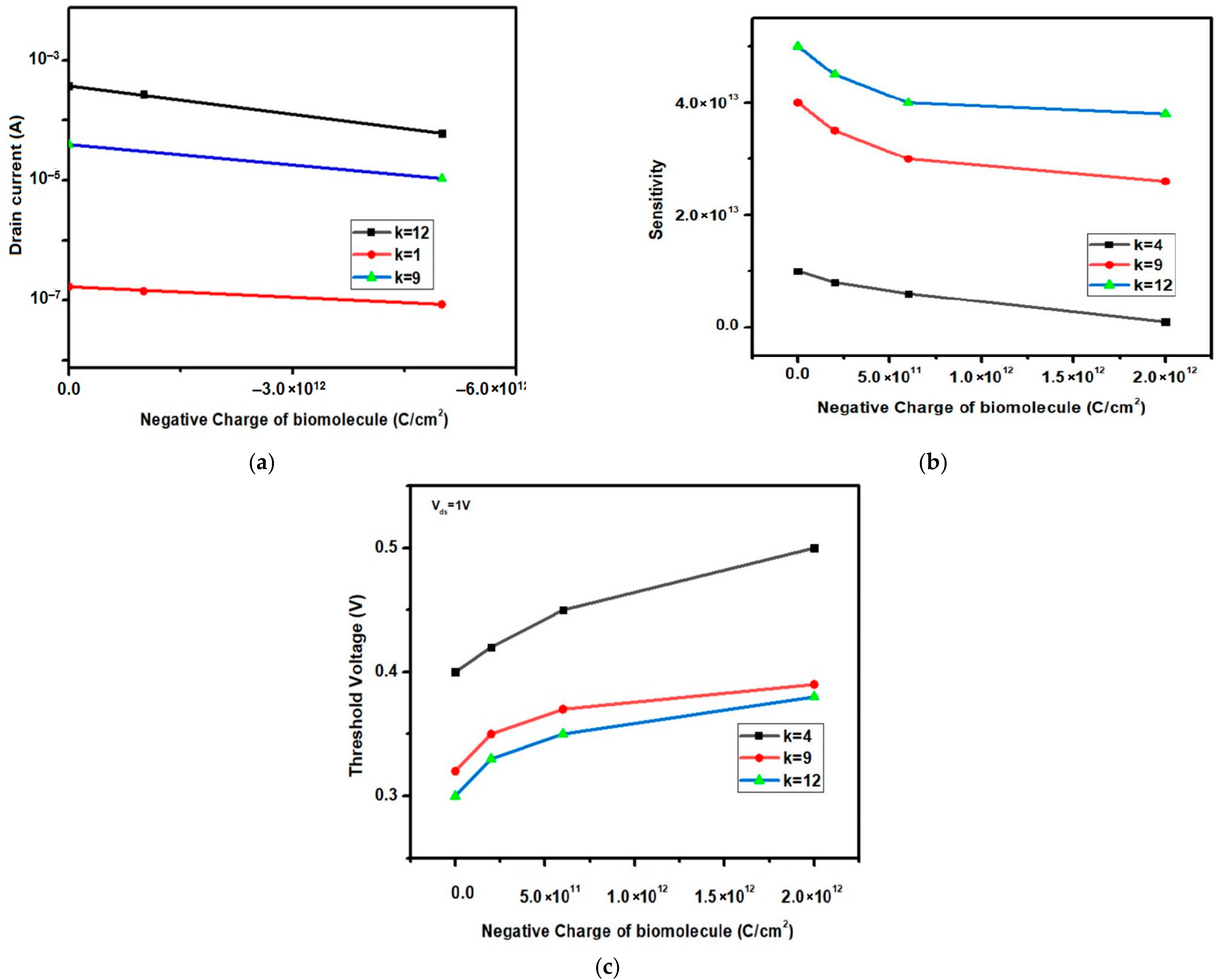
4.5.1. Threshold Voltage and Sensitivity Analysis for Negatively Charged Biomolecules
The impact of a negative charge of −1 × 10¹² C/cm2 with variation in dielectric permittivity is plotted in Figure 10a. As depicted in Figure 10b, the sensitivity shows a declining trend as the negative charge increases. However, for a fixed charge, the sensitivity increases with k. As shown in Figure 10c, the drain current shifts toward the right with an increase in negative charge, and thus, the threshold voltage increases. However, for a fixed charge, the threshold voltage increases with k. According to Equation (18), for a fixed gate voltage, the surface potential declines with an increase in negative charges, and thus, the current also declines.
4.5.2. Threshold Voltage and Sensitivity Analysis for Positively Charged Biomolecules
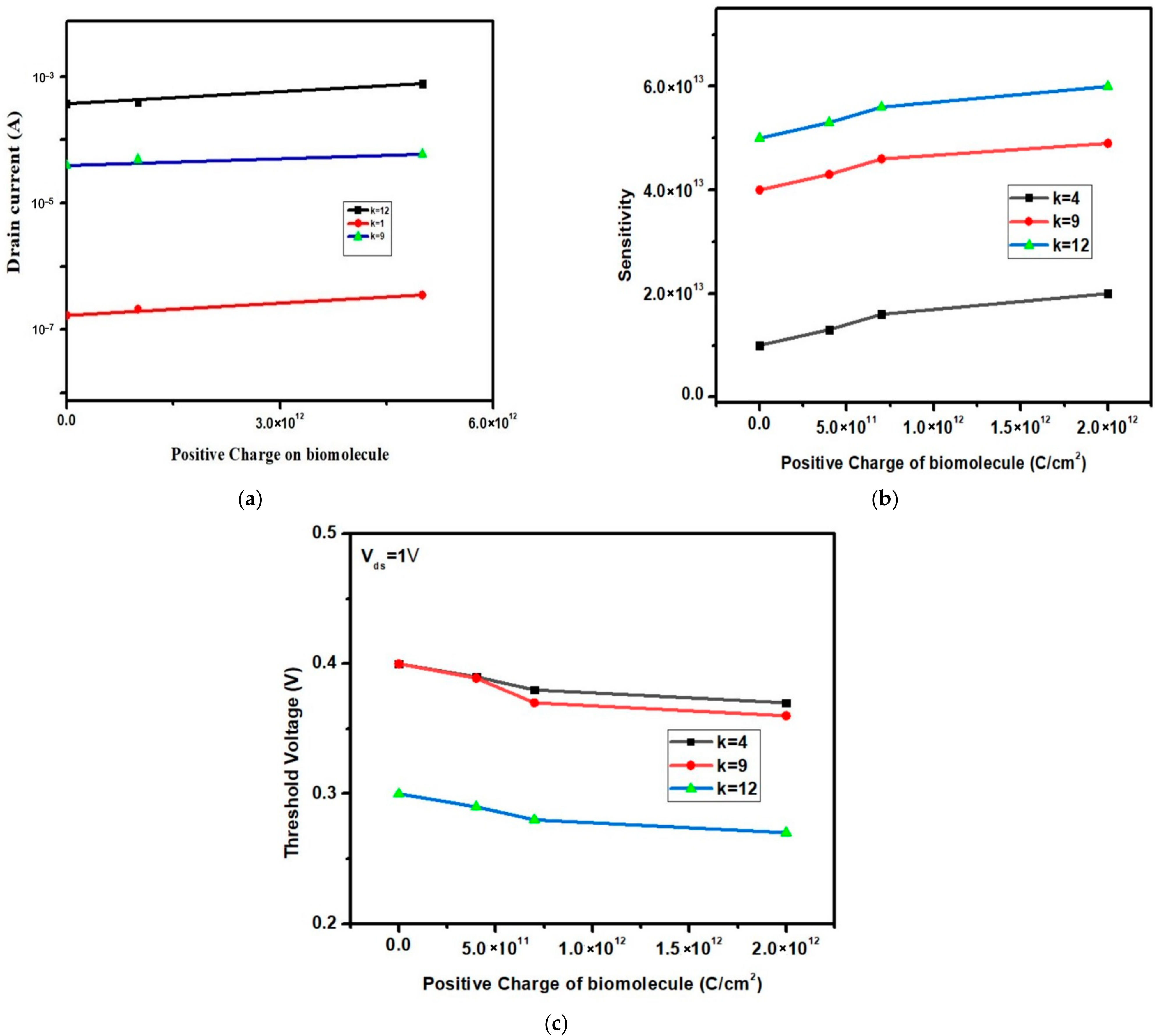
The impact of a positive charge of 1 × 10¹² C/cm2 with variation in dielectric permittivity is plotted in Figure 11a. As depicted in Figure 11b, the sensitivity increases as the magnitude of the positive charge increases. However, for a fixed charge, the sensitivity increases with the k value. As shown in Figure 11c, the drain current shifts toward the left with an increase in the positive charge, resulting in a decrease in the threshold voltage. However, for a fixed charge, the threshold voltage increases with the k value.
4.6. Impact of Fill Factor
The performance of a biosensor depends on the fraction of the cavity filled with biomolecules. Figure 12 shows the impact of the fill factor on the drain current when the cavities are 100% filled, 75% filled, and 25% filled. When the cavity is fully filled, the drain current increases, as the gate can exert maximum control over the channel, and the current increases. As the fill factor declines, the cavity has a lower number of biomolecules, and the rest of the cavity is filled with air. This means that the capacitance reduces, and this in turn results in a drop in the electric field across the tunnel junction. Thus, the current declines with a reduction in the fill factor.
4.7. Sensitivity Analysis
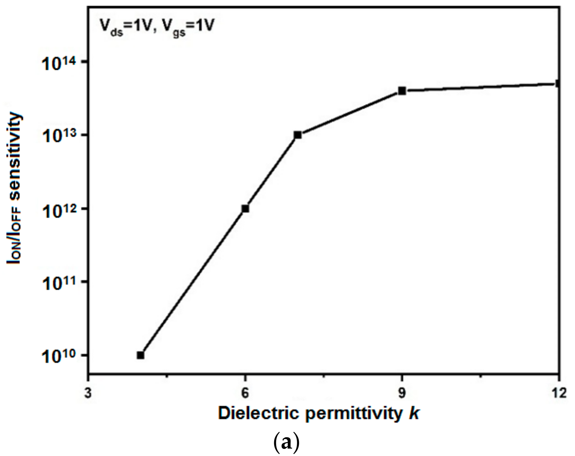
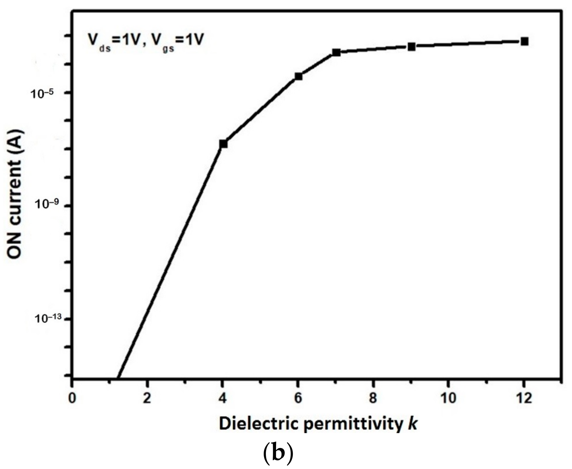
A shift in current with a change in the dielectric value is known as current sensitivity. The dielectric permittivity across the polar gate is kept fixed, whereas cavities are etched in the control gate across the tunnel junction. The performance is assessed by filling the cavities with biomolecules of different dielectrics. The performance is studied for both analyte-filled (k = 12) and empty cavities (k = 1), i.e., air-filled. The current sensitivity is determined as the ratio of the current when the cavity is filled with biomolecules of k = 12 to the current when the cavity is filled with air for a fixed gate voltage, as shown in Figure 13. As the dielectric permittivity increases, the capacitance across the cavity also increases. As a result of the resulting change in capacitance, the charge density across the junction shifts, raising the surface potential, and, consequently, the electric field across the junction increases. A higher electric field results in better coupling, leading to improved tunneling efficiency and resulting in a higher ON current. The OFF current remains more or less unaffected, thereby improving the overall current ratio.
4.7.1. Current Sensitivity
The current sensitivity calculation can be presented as follows:
The current sensitivity in the presence of biomolecules with a permittivity, k, is = 10−4. The current sensitivity in an empty cavity with k = 1 (air) is = . Vgs = constant.
4.7.2. Threshold Voltage Sensitivity
The threshold voltage (Vth) sensitivity calculation can be presented as follows:
Svoltage = Vth (air, k = 1) − Vth (bioanalyte, k = 12) = 1 V − 0.3 V = 0.7 V
4.8. Impact of Dielectric Permittivity Variation on Current Ratio (Current Sensitivity)
The impact of the variation in the dielectric constant of the material on the drain current and current ratio is depicted in Figure 13. The ON current increases with the k-value as the alignment of the band improves with an increasing dielectric permittivity. This is due to the fact that as the dielectric value increases, the gate control across the tunnel junction also improves. Moreover, with an increase in the dielectric permittivity value, the capacitance across the tunnel junction increases; i.e., the charge carrier concentration across the junction rises, which, in turn, increases the electric field across the junction. Thus, a better alignment is achieved. Moreover, as the OFF current remains almost the same, the current ratio also increases, and hence, the relative sensitivity also improves.
4.9. Impact of Dielectric Permittivity Variation on Threshold Voltage
The effect of dielectric permittivity variation on threshold voltage is shown in Figure 14. The threshold voltage is calculated by the constant current method at a 10−7 value for the ON current. We found that the threshold voltage thereby declines with a rise in the k value. As the k value increases; the coupling improves; the band alignment becomes better because of the increased electric field; and, hence, the tunneling probability becomes higher.
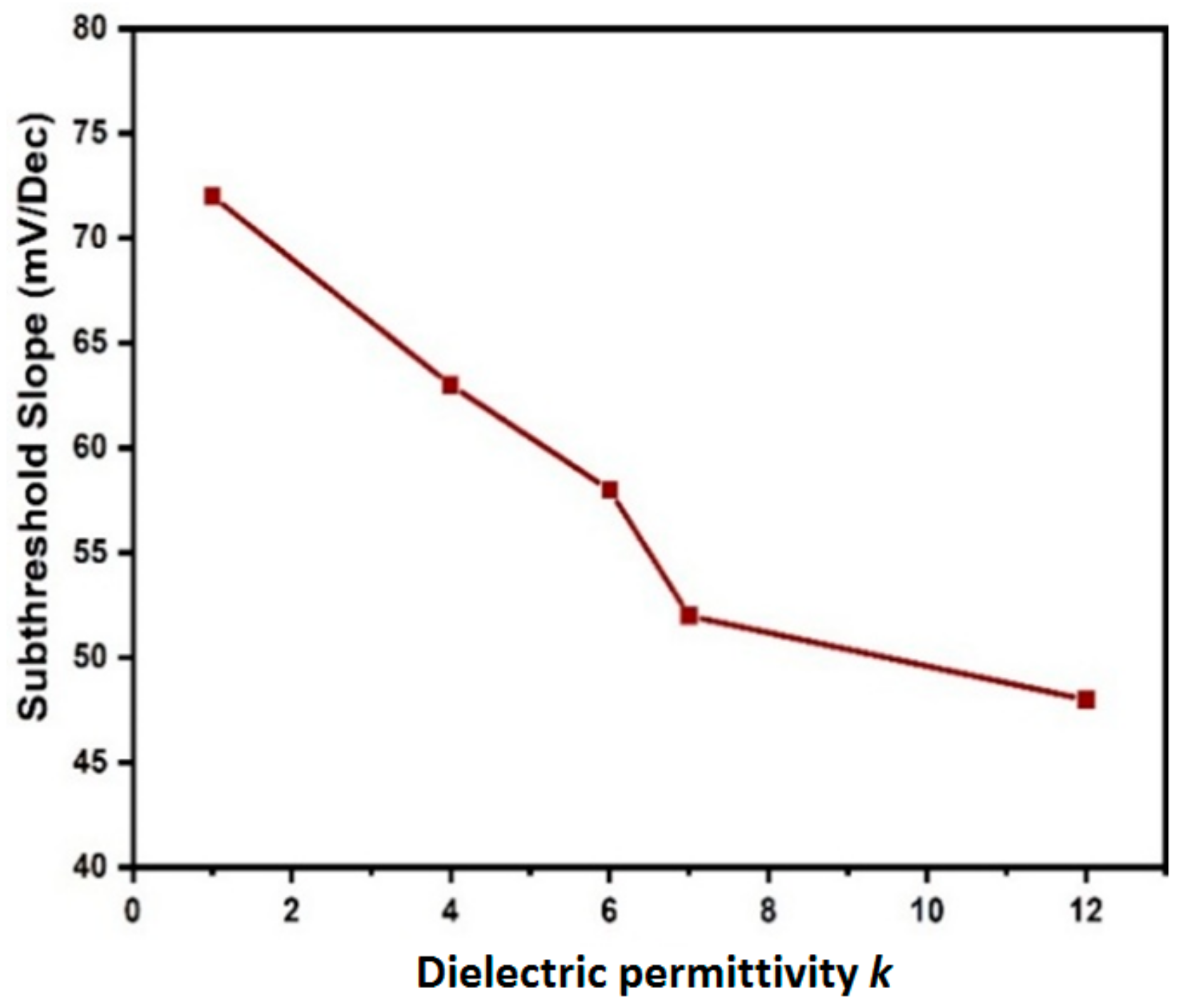
4.10. Impact of Dielectric Permittivity on Subthreshold Swing (SS)
One of the important parameters that determines the switching speed is the SS [43].
The SS of a TFET depends significantly on the tunneling phenomenon [38]. The plot in Figure 15 reflects that, for neutral biomolecules, SS decreases with an increase in the k-value. This is due to the fact that, as mentioned in the previous subsection, a higher k value will result in a higher electric field, which is why the tunneling probability increases.
4.11. Comparison with Literature
A comparative survey presented in Table 4 shows that the proposed JLTFET can achieve current sensitivities two orders of magnitude higher than competing TFET-based devices from the literature. In other words, this device is capable of achieving ION/IOFF sensitivity in the range of 1013 for current and 0.7 V for voltage change.
5. Conclusions
This work discusses the application of JLTFET-based biosensors for the detection of various biomolecules. Both the relative current sensitivity and the voltage sensitivity of the proposed sensor are analyzed, and values of 1013 and 0.7 V are reported. The analytical model of the proposed device is developed. It is solved and validated using the Sentaurus TCAD software. The impact of the position, the electric charge of the biomolecules, the fill factor, and the size of the cavity are also studied. The device not only exhibits a significantly improved relative current sensitivity in comparison with the existing FET and TFET-based biosensors but also shows itself to be practical for low-power uses. Thus, a dielectric-modulation-based design opens a pathway to improved performance and offers a wide range of possibilities for future research and applications.
Author Contributions
Conceptualization, S.C.; methodology, S.C. and K.L.B.; software, S.C.; validation, K.L.B., K.G., J.I. and Z.J.; formal analysis, S.C.; investigation, S.C.; design and simulation, S.C.; writing—original draft preparation, S.C.; writing—review and editing, S.C., K.L.B., K.G., J.I., Z.J. and O.J.; visualization, S.C.; supervision, K.L.B.; project administration, K.L.B. and K.G.; funding acquisition, K.G., J.I., Z.J. and O.J. All authors have read and agreed to the published version of the manuscript.
Funding
All authors besides O.J. declare that no funds, grants, or other support were received during the preparation of this manuscript. O.J. declares that her work was supported by the Ministry of Science, Technological Development, and Innovations of the Republic of Serbia through grant 451-03-47/2023-01/200026.
Institutional Review Board Statement
Not applicable.
Informed Consent Statement
Not applicable.
Data Availability Statement
Data and materials supporting the research are found within the manuscript. Raw data files will be provided by the corresponding author upon request.
Acknowledgments
This publication is an outcome of the R&D work undertaken for the project under the Visvesvaraya Scheme of the Ministry of Electronics and Information Technology, Government of India, implemented by the Digital India Corporation (formerly Media Lab Asia).
Conflicts of Interest
The authors declare no conflict of interest.
References
- Cui, Y.; Wei, Q.; Park, H.; Lieber, C.M. Nanowire nano-sensors for highly sensitive and selective detection of biological and chemical species. Science 2001, 293, 1289–1292. [Google Scholar] [CrossRef] [PubMed]
- Yang, N.; Chen, X.; Ren, T.; Zhang, P.; Yang, D. Carbon nanotube-based biosensors. Sens. Actuators B Chem. 2015, 207, 690–715. [Google Scholar] [CrossRef]
- Byon, H.R.; Choi, H.C. Network single-walled carbon nanotube-field effect transistors (SWNT-FETs) with increased Schottky contact area for highly sensitive biosensor applications. J. Am. Chem. Soc. 2006, 128, 2188–2189. [Google Scholar] [CrossRef]
- Tang, X.; Bansaruntip, S.; Nakayama, N.; Yenilmez, E.; Chang, Y.I.; Wang, Q. Carbon nanotube DNA sensor and sensing mechanism. Nano Lett. 2006, 6, 1632–1636. [Google Scholar] [CrossRef]
- Star, J.C.; Gabriel, P.; Bradley, K.; Grüner, G. Electronic detection of specific protein binding using nanotube FET devices. Nano Lett. 2003, 3, 459–463. [Google Scholar] [CrossRef]
- Alam, M.Z.; Alimuddin; Khan, S.A. A Review on Schiff Base as a Versatile Fluorescent Chemo-sensors Tool for Detection of Cu2+ and Fe3+ Metal Ion. J. Fluoresc. 2023, 13, 1–32. [Google Scholar] [CrossRef]
- Alam, M.Z.; Khan, S.A. A review on Rhodamine-based Schiff base derivatives: Synthesis and fluorescent chemo-sensors behaviour for detection of Fe3+ and Cu2+ ions. J. Coord.Chem. 2023, 76, 371–402. [Google Scholar] [CrossRef]
- Naresh, V.; Lee, N. A Review on Biosensors and Recent Development of Nanostructured Materials-Enabled Biosensors. Sensors 2021, 21, 1109. [Google Scholar] [CrossRef]
- Singh, A.; Sharma, A.; Ahmed, A.; Sundramoorthy, A.K.; Furukawa, H.; Arya, S.; Khosla, A. Recent Advances in Electrochemical Biosensors: Applications, Challenges, and Future Scope. Biosensors 2021, 11, 336. [Google Scholar] [CrossRef] [PubMed]
- Chen, C.; Wang, J. Optical biosensors: An exhaustive and comprehensive review. Analyst 2020, 145, 1605–1628. [Google Scholar] [CrossRef]
- Karimi-Maleh, H.; Orooji, Y.; Karimi, F. A critical review on the use of potentiometric based biosensors for biomarkers detection. Biosens. Bioelectron. 2021, 184, 113252. [Google Scholar] [CrossRef] [PubMed]
- Ramanathan, K.; Danielsson, B. Principles and applications of thermal biosensors. Biosens. Bioelectron. 2001, 16, 417–423. [Google Scholar] [CrossRef] [PubMed]
- Narang, R.; Saxena, M.; Gupta, M. Comparative Analysis of Dielectric-Modulated FET and TFET-Based Biosensor. IEEE Trans. Nanotechnol. 2015, 14, 427–435. [Google Scholar] [CrossRef]
- Kataoka, H.; Miyahara, Y. Label-free detection of DNA by field-effect devices. IEEE Sens. J. 2011, 11, 3153–3160. [Google Scholar] [CrossRef]
- Sarkar, S.; Banerjee, K. Fundamental limitations of conventional-FET biosensors: Quantum-mechanical-tunneling to the rescue. In Proceedings of the 70th Device Research Conference, University Park, PA, USA, 18–20 June 2012; pp. 83–84. [Google Scholar] [CrossRef]
- Narang, R.; Reddy, K.V.S.; Saxena, M.; Gupta, R.S.; Gupta, M. A Dielectric-Modulated Tunnel-FET-Based Biosensor for Label-Free Detection: Analytical Modeling Study and Sensitivity Analysis. IEEE Trans. Electron Devices 2012, 59, 2809–2817. [Google Scholar] [CrossRef]
- Narang, R.; Saxena, M.; Gupta, R.S.; Gupta, M. Dielectric Modulated Tunnel Field-Effect Transistor—A Biomolecule Sensor. IEEE Electron Device Lett. 2012, 33, 266–268. [Google Scholar] [CrossRef]
- Kanungo, S.; Chattopadhyay, S.; Gupta, P.S.; Rahman, H. Comparative Performance Analysis of the Dielectrically Modulated Full-Gate and Short-Gate Tunnel FET-Based Biosensors. IEEE Trans. Electron Devices 2015, 62, 994–1001. [Google Scholar] [CrossRef]
- Anam, A.; Anand., S.; Amin, S.I. Design and Performance Analysis of Tunnel Field Effect Transistor with Buried Strained Si1−xGex Source Structure Based Biosensor for Sensitivity Enhancement. IEEE Sens. J. 2020, 20, 13178–13185. [Google Scholar] [CrossRef]
- Narang, R.; Saxena, M.; Gupta, R.S.; Gupta, M. Analytical Model for a Dielectric Modulated Double Gate FET (DM-DG-FET) Biosensor. In Proceedings of the International Conference on Emerging Electronics, Bangalore, India, 11–14 December 2022; pp. 1–4. [Google Scholar] [CrossRef]
- Shafi, N.; Sahu, C.; Periasamy, C. Virtually doped Si-Ge tunnel FET for enhanced sensitivity in biosensing applications. Superlattices Microstruct. 2018, 120, 75–89. [Google Scholar] [CrossRef]
- Anand, S.; Singh, A.; Amin, S.I.; Thool, A.S. Design and performance analysis of dielectrically modulated doping-less tunnel FET-based label free biosensor. IEEE Sens. J. 2019, 19, 4369–4374. [Google Scholar] [CrossRef]
- Narang, R.; Saxena, M.; Gupta, M. Modeling and simulation investigation of sensitivity of symmetric split gate Junctionless FET for biosensing application. IEEE Sens. J. 2017, 17, 4853–4861. [Google Scholar] [CrossRef]
- Singh, S.; Raj, B.; Vishvakarma, S.K. Analytical modeling of split gate junction-less transistor for a biosensor application. Sens. Biosens. Res. 2018, 18, 31–36. [Google Scholar] [CrossRef]
- Ghosh, B.; Akram, M.W. Junction less Tunnel Field Effect Transistor. IEEE Electron Device Lett. 2013, 34, 584–586. [Google Scholar] [CrossRef]
- Chakraborty, A.; Singha, D.; Sarkar, A. Staggered heterojunctions-based tunnel-FET for application as a label-free biosensor. Int. J. Nanopart. 2018, 10, 107–116. [Google Scholar] [CrossRef]
- Gao, N.; Lu, N.; Wang, Y. Robust ultrasensitive tunneling-FET biosensor for point-of-care diagnostics. Sci. Rep. 2016, 6, 22554. [Google Scholar] [CrossRef] [PubMed]
- Choudhury, S.; Baishnab, K.L.; Bhowmik, B.; Guha, K. Design and optimization of asymmetrical TFET. In Microsystem Technologies; Springer, SCI: Berlin/Heidelberg, Germany, 2021; Volume 27, pp. 3457–3464. [Google Scholar] [CrossRef]
- Gupta, S.K.; Kumar, S. Analytical Modeling of a Triple Material Double Gate TFET with Hetero-Dielectric Gate Stack. Silicon 2018, 11, 1355–1369. [Google Scholar] [CrossRef]
- Darwin, S.; ASTS. Mathematical Modeling of Junctionless Triple Material Double Gate MOSFET for Low Power Applications. J. Nano Res. 2019, 56, 71–79. [Google Scholar] [CrossRef]
- Priya, G.L.; Balamurugan, N.B. New dual material double gate junctionless tunnel FET: Subthreshold modeling and simulation. AEU Int. J. Electron. Commun. 2019, 99, 130–138. [Google Scholar] [CrossRef]
- Im, H.; Huang, X.J.; Gu, B.; Choi, Y.K. A dielectric-modulated field-effect transistor for biosensing. Nat. Nanotechnol. 2007, 2, 430–434. [Google Scholar] [CrossRef]
- Sharma, D.; Singh, D.; Pandey, S.; Yadav, S.; Kondekar, P.N. Comparative analysis of full-gate and short-gate dielectric modulated electrically doped Tunnel-FET based biosensors. Superlattice Microstruct. 2017, 111, 767–775. [Google Scholar] [CrossRef]
- Venkatesh, P.; Nigam, K.; Pandey, S.; Yadav, S.; Kondekar, P.N. A dielectrically modulated electrically doped tunnel FET for application of label free biosensor. Superlattice Microstruct. 2017, 109, 470–479. [Google Scholar] [CrossRef]
- Verma, M.; Tirkey, S.; Yadav, S.; Sharma, D.; Yadav, D.S. Performance assessment of a novel vertical dielectrically modulated TFET-based biosensor. IEEE Trans. Electron Devices 2017, 64, 3841–3848. [Google Scholar] [CrossRef]
- Devi, W.V.; Bhowmick, B. Optimization of Pocket doped Junctionless TFET and its Application in digital Inverter. Micro Nano Lett. 2018, 14, 69–73. [Google Scholar] [CrossRef]
- INTERNATIONAL. International Technology Roadmap for Semiconductor; INTERNATIONAL: New York, NY, USA, 2018; Available online: Ieee.org (accessed on 28 July 2022).
- Hussain, S. A comprehensive study on tunneling field effect transistor using non-local band-to-band tunneling model. J. Phys. Conf. Ser. 2020, 1432, 012028. [Google Scholar] [CrossRef]
- Bal, P.; Ghosh, B.; Mondal, P. Dual material gate junctionless tunnel field effect transistor. J. Comput. Electron. 2014, 13, 230–234. [Google Scholar] [CrossRef]
- Soni, D.; Sharma, D.; Aslam, M.; Yadav, S. Approach for the improvement of sensitivity and sensing speed of TFET-based biosensor by using plasma formation concept. Micro Nano Lett. 2018, 13, 1728–1733. [Google Scholar] [CrossRef]
- Zweckstetter, M.; Hummer, G.; Bax, A. Prediction of Charge-Induced Molecular Alignment of Biomolecules Dissolved in Dilute Liquid-Crystalline Phases. Biophys. J. 2004, 86, 3444–3460. [Google Scholar] [CrossRef] [PubMed]
- Lee, J.; Kim, M.J.; Yang, H.; Kim, S.; Yeom, S.; Ryu, G.; Shin, Y.; Sul, O.; Jeong, J.K.; Lee, S.-B. Extended-Gate Amorphous InGaZnO Thin Film Transistor for Biochemical Sensing. IEEE Sens. J. 2020, 21, 178–184. [Google Scholar] [CrossRef]
- Kanungo, S.; Chattopadhyay, S.; Gupta, P.S. Study and analysis of the effects of Si-Ge source and pocket doped channel on sensing performance of dielectrically modulated tunnel FET based biosensor. IEEE Trans. Electron Devices 2016, 63, 2589–2596. [Google Scholar] [CrossRef]
Figure 1.
Proposed DM-JLTFET as a biosensor.

Figure 2.
Calibration of the simulated model with a conventional JLTFET.

Figure 3.
Energy band diagram of a DM-JLTFET as a biosensor for k = 12 (dashed and dash-dotted lines) and k = 1 (solid lines). The green arrow shows the tunnel width.
Figure 3.
Energy band diagram of a DM-JLTFET as a biosensor for k = 12 (dashed and dash-dotted lines) and k = 1 (solid lines). The green arrow shows the tunnel width.

Figure 4.
Surface potential along the channel for different permittivities.

Figure 5.
Comparison of surface potential values along the microchannel—analytical model (solid lines) vs. simulation (dashed).
Figure 5.
Comparison of surface potential values along the microchannel—analytical model (solid lines) vs. simulation (dashed).

Figure 6.
Variation in drain current versus gate voltage for biomolecules with different values of dielectric permittivity: a comparison of analytical and simulated results.
Figure 6.
Variation in drain current versus gate voltage for biomolecules with different values of dielectric permittivity: a comparison of analytical and simulated results.

Figure 7.
Drain current versus gate voltage for different cavity lengths.

Figure 8.
Drain current versus gate voltage for different values of the cavity thickness.

Figure 9.
(a) Drain current versus gate voltage for different values of electric charge in biomolecules. (b) Enlarged part of the current–voltage dependence shown in (a).
Figure 9.
(a) Drain current versus gate voltage for different values of electric charge in biomolecules. (b) Enlarged part of the current–voltage dependence shown in (a).

Figure 10.
(a) Drain current for negative molecules, −1 × 10¹² C/cm2 with permittivity variation. (b) Sensitivity as a function of a negative charge with permittivity variation. (c) Threshold voltage as a function of negative charge with permittivity variation.
Figure 10.
(a) Drain current for negative molecules, −1 × 10¹² C/cm2 with permittivity variation. (b) Sensitivity as a function of a negative charge with permittivity variation. (c) Threshold voltage as a function of negative charge with permittivity variation.

Figure 11.
(a) Drain current for positive molecules, 1 × 10¹² C/cm2 with permittivity variation. (b) Sensitivity as a function of a positive charge. (c) Threshold voltage as a function of a positive charge.
Figure 11.
(a) Drain current for positive molecules, 1 × 10¹² C/cm2 with permittivity variation. (b) Sensitivity as a function of a positive charge. (c) Threshold voltage as a function of a positive charge.

Figure 12.
Drain current versus gate voltage for various fill factors.

Figure 13.
(a) Current sensitivity (ON/OFF current ratio) dependence on k-value. (b) ON current dependence on k-value.
Figure 13.
(a) Current sensitivity (ON/OFF current ratio) dependence on k-value. (b) ON current dependence on k-value.


Figure 14.
Threshold voltage dependence on dielectric permittivity.

Figure 15.
Subthreshold slope dependence on dielectric permittivity, d.


Table 1.
Parameter values for biosensor design.
| Parameters | Values |
|---|---|
| L1 | 5 nm |
| L2 | 5–10 nm |
| L3 | 5–10 nm |
| 1 nm | |
| 2 nm | |
| 1 nm | |
| 5 nm | |
| 4.1 eV | |
| (Co) | 4.7 eV |
| (Sc) | 4.0 eV |
| 5–7 nm | |
| 10–30 nm | |
| Bioanalyte permittivities | k = 1–12 |
Table 2.
A comparison with reference works.
| References | ION (A/μm) | IOFF (A/μm) | Ratio | Vth (V) | SS (Average) mV/dec | SS (Point) mV/dec |
|---|---|---|---|---|---|---|
| Ref. [25] | 36 × 10−6 | 5 × 10⁻¹⁴ | 6 × 10⁸ | 0.4 | 70 | 38 |
| Ref. [30] | 1 × 10⁻⁶ | 1 × 10⁻¹³ | 6 × 10⁷ | 0.8 | 48 | - |
| Ref. [39] | 18 × 10−5 | 3 × 10⁻¹³ | 6 × 10⁸ | 0.4 | - | 17 |
| Present work (k = 12) | 3 × 10⁻⁴ | 2.4 × 10⁻¹⁷ | 1.2 × 10¹³ | 0.3 | 48 | 9 |
Table 3.
Dielectric permittivity values.
| Parameters | Values for k |
|---|---|
| Air | 1 |
| Ferro-cytochrome | 4 |
| Biotin | 2 |
| Bacteriophage T7 | 6 |
| Zein | 7 |
| Keratin | 9 |
| Gelatin | 12 |
Disclaimer/Publisher’s Note: The statements, opinions and data contained in all publications are solely those of the individual author(s) and contributor(s) and not of MDPI and/or the editor(s). MDPI and/or the editor(s) disclaim responsibility for any injury to people or property resulting from any ideas, methods, instructions or products referred to in the content. |
© 2023 by the authors. Licensee MDPI, Basel, Switzerland. This article is an open access article distributed under the terms and conditions of the Creative Commons Attribution (CC BY) license (https://creativecommons.org/licenses/by/4.0/).
Share and Cite
MDPI and ACS Style
Choudhury, S.; Baishnab, K.L.; Guha, K.; Jakšić, Z.; Jakšić, O.; Iannacci, J. Modeling and Simulation of a TFET-Based Label-Free Biosensor with Enhanced Sensitivity. Chemosensors 2023, 11, 312. https://doi.org/10.3390/chemosensors11050312
AMA Style
Choudhury S, Baishnab KL, Guha K, Jakšić Z, Jakšić O, Iannacci J. Modeling and Simulation of a TFET-Based Label-Free Biosensor with Enhanced Sensitivity. Chemosensors. 2023; 11(5):312. https://doi.org/10.3390/chemosensors11050312
Chicago/Turabian StyleChoudhury, Sagarika, Krishna Lal Baishnab, Koushik Guha, Zoran Jakšić, Olga Jakšić, and Jacopo Iannacci. 2023. "Modeling and Simulation of a TFET-Based Label-Free Biosensor with Enhanced Sensitivity" Chemosensors 11, no. 5: 312. https://doi.org/10.3390/chemosensors11050312
Note that from the first issue of 2016, this journal uses article numbers instead of page numbers. See further details here.