Article

Miniaturized Compact Reconfigurable Half-Mode SIW Phase Shifter with PIN Diodes

Department of Computer Science and Engineering, University of Quebec in Outaouais (UQO), Gatineau, QC J8Y 3G5, Canada
*
Author to whom correspondence should be addressed.
Technologies 2023, 11(3), 63; https://doi.org/10.3390/technologies11030063
Submission received: 1 March 2023 / Revised: 8 April 2023 / Accepted: 21 April 2023 / Published: 23 April 2023
(This article belongs to the Special Issue Perpetual Sensor Nodes for Sustainable Wireless Network Applications)

Abstract

:
In this work, a novel electrically reconfigurable phase shifter based on a half-mode substrate integrated waveguide (HM-SIW) is proposed. SIW is a guided transmission line topology, and by using half-mode excitation, a smaller size can be achieved. Phase shifters are electronic devices that change the phase of transmission for a wide range of applications, including inverse scattering and sensing. The tunability of PIN diodes is applied here to achieve a reconfigurable design. The proposed single-layer structure does not require extra wiring layers for the bias circuit on the suggested printed circuit board. Its principle consists in the integration, in the HM-SIW, of three parallel lines, each connecting the edge of the HM-SIW and linked to a PIN diode and a radial stub. Here we present the results of measurements for a frequency band from 4.5 to 7 GHz that demonstrate how the experiment agrees with simulations. Insertion loss was less than −10 dB, and port coupling was less than −2 dB for both simulation and measurement solutions. The proposed half-mode structure is around half the size of a typical SIW line. With the proposed design, the seven states of the PIN diodes can be validated (ON and OFF), with a wide band adaptation and a relatively constant phase difference across a broad frequency range (44%). A key benefit of the proposed design for a microwave component is the reduction of extra biasing layers for the PIN diodes. This is in addition to the reduced size of the transmission line compared to a commercial SIW. In the annexed section, simulation software is used for a more comprehensive analysis involving more phase shift values and parametric studies.

1. Introduction

The phase shifter is a key microwave circuit in modern communication, especially when designing a phase array system [1,2,3,4]. In multidisciplinary antenna devices, a phase shifter can be used to feed both the transmit and receive sections [5,6,7,8]. However, a phase shifter is a more practical method of identifying information due to the low amount of power and linearity features at reception [9]. Currently, phase shifters are mainly applied to the electronic beam control of an antenna in a phased array system [10,11,12,13,14]. This is to improve the quality of the coverage area in transmission as well as in high-speed reception. Other applications are cavity filters, power dividers, phase modulators, high power devices, and radars [15]. Phase shifters can be designed using passive or active elements.
According to the literature, there are different types of phase shifters [16,17]. We can create phase shifts based on transmission lines to create an arbitrary degree of phase shift in a frequency band [16]. This technique has been applied to Schiffman-coupled differential transmission lines. Furthermore, high-power handling waveguides can generate a phase step from a multi-step ridge section along a shift guided line [17]. Moreover, filtering mechanisms undergo different transmission line comparisons for phase shifting. With this mechanism, it is possible to provide constant phase delays [18]. A dual-band phase shifter has been proposed by comparing two different transmission lines for two distinct phase shifts [19]. A more complex structure has been applied to design a tunable filter phase shifter at 1 GHz frequency with two power dividers and two reconfigurable filter couplers [20]. Additionally, substrate-integrated waveguides (SIW), as a new generation of transmission lines [21,22,23], can be configured for phase-shifting microwave networks [24,25,26]. Added metal posts to change SIW resonators [24], slots on the upper surface of the SIW [25], high dielectric constant perturbation [26,27], fixed cross-sectional elements [28], and coupled slots [29] are some of the models presented to develop a SIW phase shifter.
Many of these methods generate a fixed phase difference between two points in the microwave component. However, it is highly desirable to create a modular or reconfigurable phase shifter device. In particular, a compact and miniaturized element is required that can be easily integrated with other microwave-packaged components. By using a diode and its related states, one can tune the constant phase shifter structure as studied in [30,31]. The PIN diodes can interact with the SIW line to change the required phase difference while the signal travels through the line. Integration of diodes in an electromagnetic device is not straightforward and requires innovative aspects regarding diode state change. An example of a technique presented in a patent from 2022 involves eliminating the need for additional biasing lines for PIN diodes used in beam switching applications [32]. This algorithm is suggested to generate a phase shifter microwave component in this novel progressive work. The intervention load parameters may also be modified by using a varactor and capacitor in addition to the PIN diodes [33,34,35]. However, a PIN diode could provide a more stable and quicker response to bias and RF sources.
With a tapered microstrip choke and resistor in one united layer, radio frequency (RF) signals and DC current are isolated [36]. In order to separate two energy sources and their functionality, this step must be taken. In addition to the required phase shift and simple one-layer design, it is necessary to reduce the total surface of a compact microwave device. As a result, we propose a half-mode SIW to realize a novel practical electronic device. The half-mode SIW is smaller and performs similarly to a typical SIW phase shifter. The proposed structure can be applied to miniaturized RF circuits to generate desirable phase shifts. A similar dielectric constant must exist to compare the width and size of a phase shifter component to determine the amount of miniaturization. Using the concept of magnetic wall, this paper proposes the steps for designing a new half-mode substrate integrated waveguide (HM-SIW), which presents all the advantages of a SIW but with a size reduced by half [37,38,39]. Thus, three microstrip lines are connected to three PIN diodes, which are connected at each end to a radial stub. This circuit generates an electrically controllable phase shift between the two ports of a HM-SIW thanks to the eight active states of the diodes associated with the radial stubs. To validate the proposed design, we used several simulation techniques and a concrete measurement step. The length and width of the microstrip lines and their location on the HM-SIW are optimized to have an approximately constant phase shift over the considered frequency range. The rest of the paper is organized as follows: Section 2 presents the design of the HM-SIW and the proposed HM-SIW phase shifter component. Simulation results and fabricated circuit tests for optimized structures are presented in Section 3. Moreover, concluding remarks are given in Section 4. In addition, two useful Appendix A and Appendix B that investigate a high phase shift feature and some parametric studies with the same proposed technology from simulation software have been prepared.

2. Design of the HM-SIW Phase Shifter

The proposed HM-SIW consists of a one-layer substrate, and the background is covered with copper all around. The substrate material is Rogers RT/duroid 5880 with 2.2 relative permittivity (εr), 0.508 mm thickness, and 0.0009 loss tangent. The first step in a reconfigurable compact modular phase shifter design is to create a proper transmission line. This transfers signals within the frequency band with low dissipation.

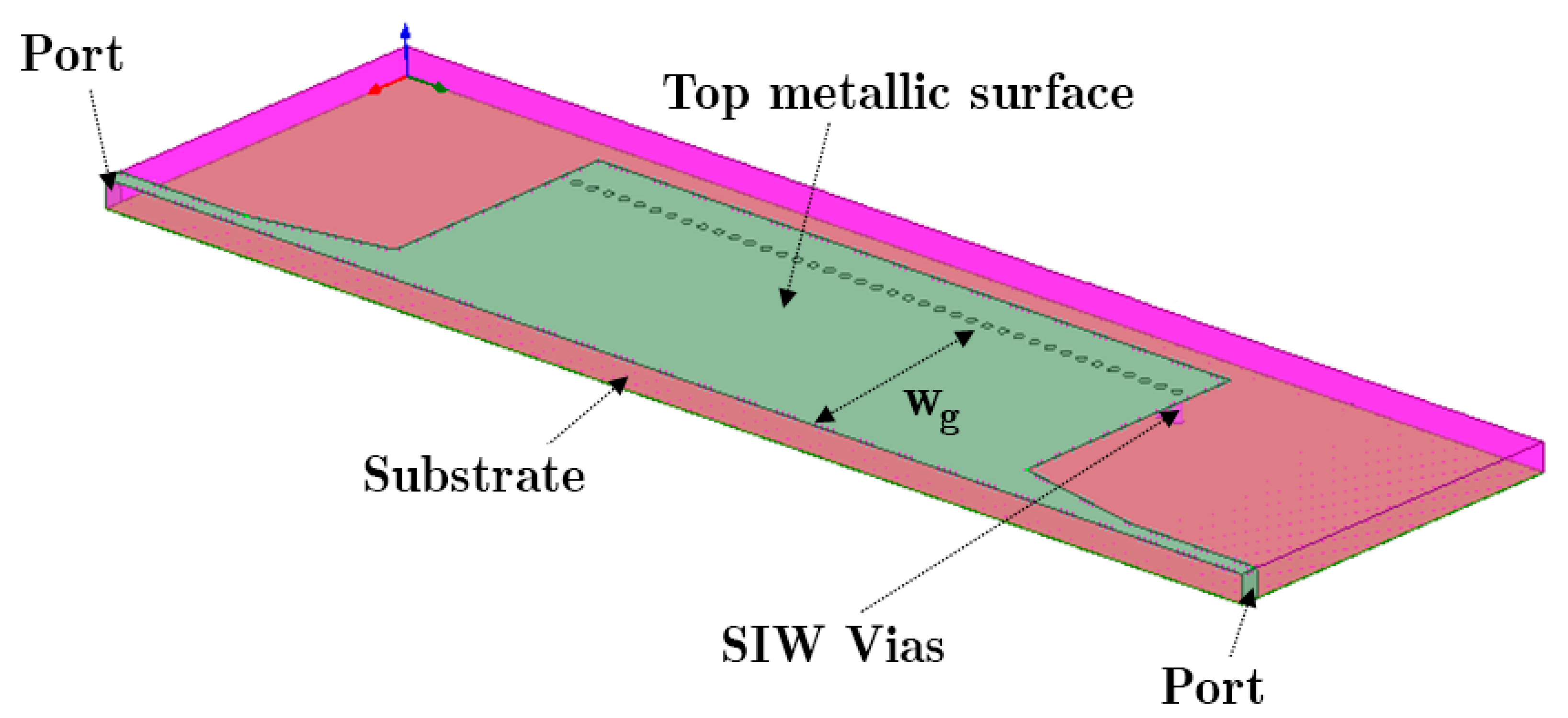
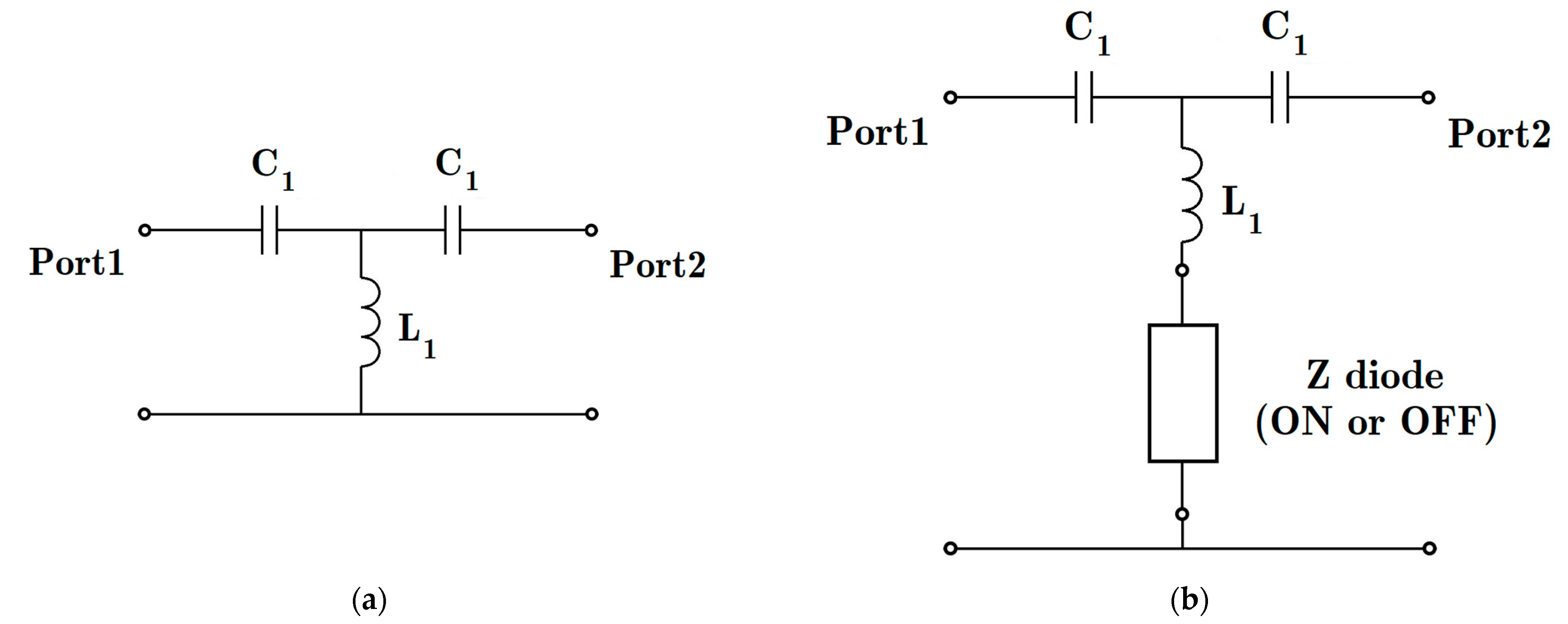
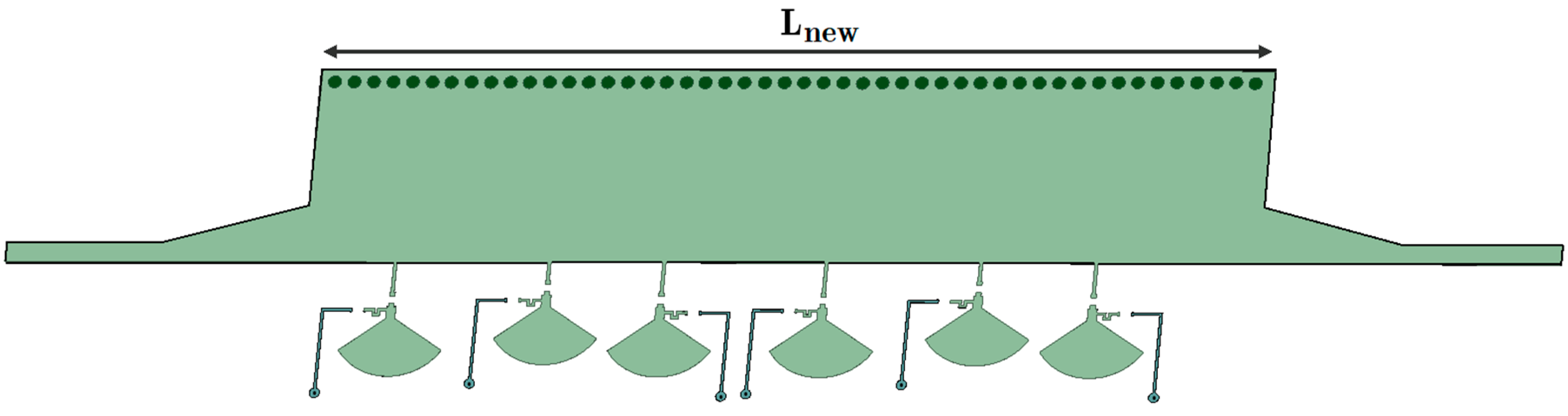
2.1. Transmission Line Topology

Figure 1 illustrates the geometric parameters of a HM-SIW structure that transfers a desired signal. The width of the transmission line can be reduced when using a half-mode SIW, but on the other hand, most of the SIW features are still maintained. Instead of vias in both corners, one edge will be an open aperture.
Dividing a SIW transmission line in half creates the HM-SIW. On the open aperture plane, the magnetic field is nearly parallel, which creates an equivalent perfect magnetic conductor. This topology can handle a lower amount of signal transmission power and requires a smaller frequency wavelength compared to the thickness of the substrate. Both of the aforementioned facts are acceptable for electronically controlled phase shifter designs and the desired operation frequency of 4~8 GHz.
In addition, the port widths are configured to transmit 50 Ω from microstrip line theory [40]. This configuration is being continued to prepare a constant matching feature to be used with the HM-SIW structure. A typical microstrip line has been used to feed the proposed structure. For adequate impedance matching, the microstrip line segment connecting the SIW has been tapered. We refer to the employed structure as the microstrip to SIW transition [41].
Starting from the cutoff frequency and exploiting the operating conditions of a SIW line, width (Wg), pitch, or distance between the vias (p), and via diameter (d) can be formed. Equations (1)–(9) describe the conditions that govern SIW operation in dominant mode [42]. Then, by exploiting the phenomenon of the magnetic wall, we can define HM-SIW [43].
λ g = c 0 r   ,
λ 2   <   W e f f   <   λ ,
p   <   d (Physically realizable condition of vias.),
p λ g   <   0.25 (avoiding bandgap),
d < λ g 5 ,   and   p 2 d   (reducing radiation loss),
p λ c > 0.05   (avoiding over perforation),
W eff = W g 1.08 d 2 p + 0.1 d 2 W g   ,
p d < 3 ,   and   d W g < 0.2   (accurate range),
L eff = L 1.08 d 2 p + 0.1 d 2 L   ,
where c0, λg, Leff, and Weff are, respectively, the speed of light, guided wavelength, effective length, and width [44]. Equations (1) and (2) are applied to calculate the transmission line geometry for 4 GHz when modeling SIW with a dielectric-filled rectangular waveguide. Then, the Weff is split in half for a half-mode SIW. Furthermore, the diameter of the via (d) and the distance between the vias (p) are set up with Equations (3)–(9) and the fabrication limits. The diameter of the via holes is d = 1.016 mm, and the distance between two via centers is p = 1.5 mm. Each via is 0.492 mm away from the metal edge, and Wg = 15 mm.

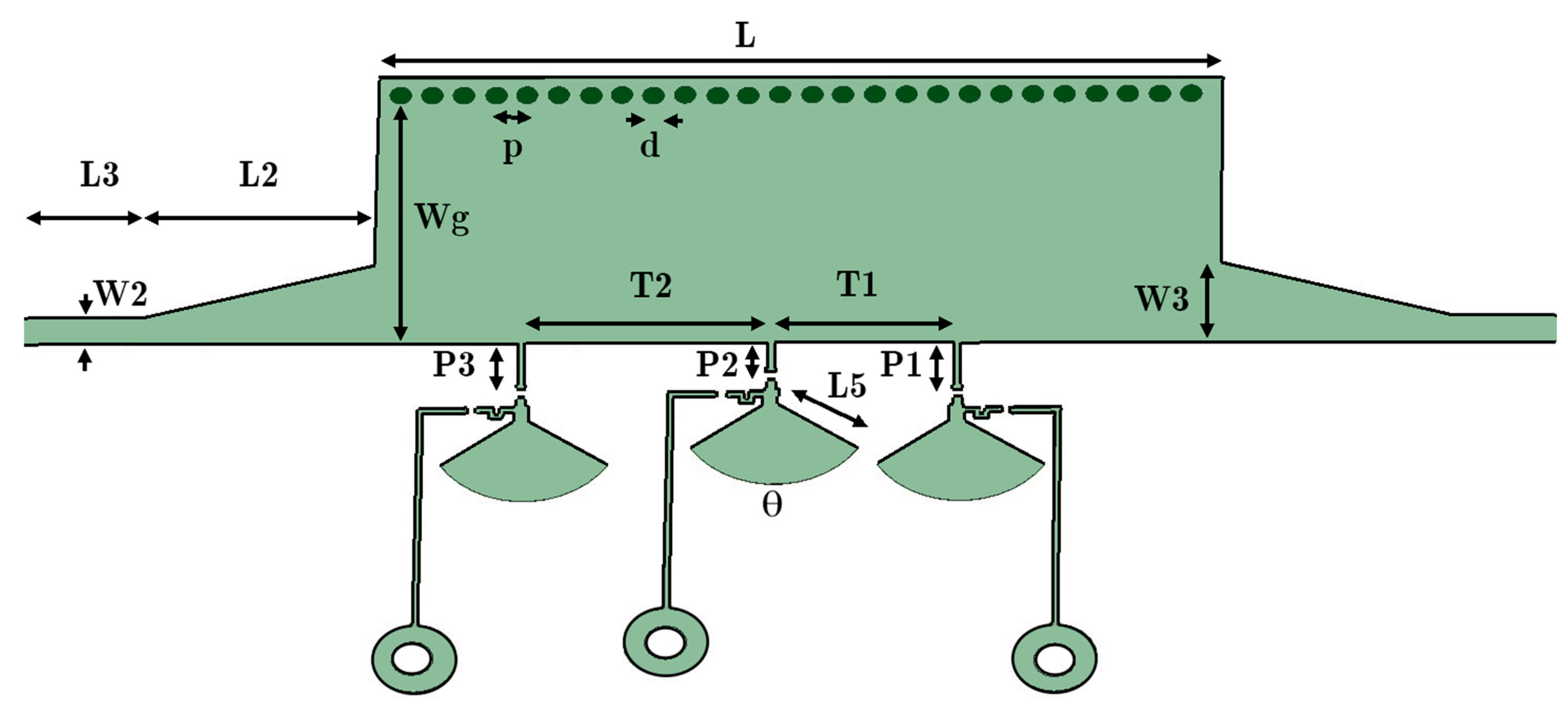
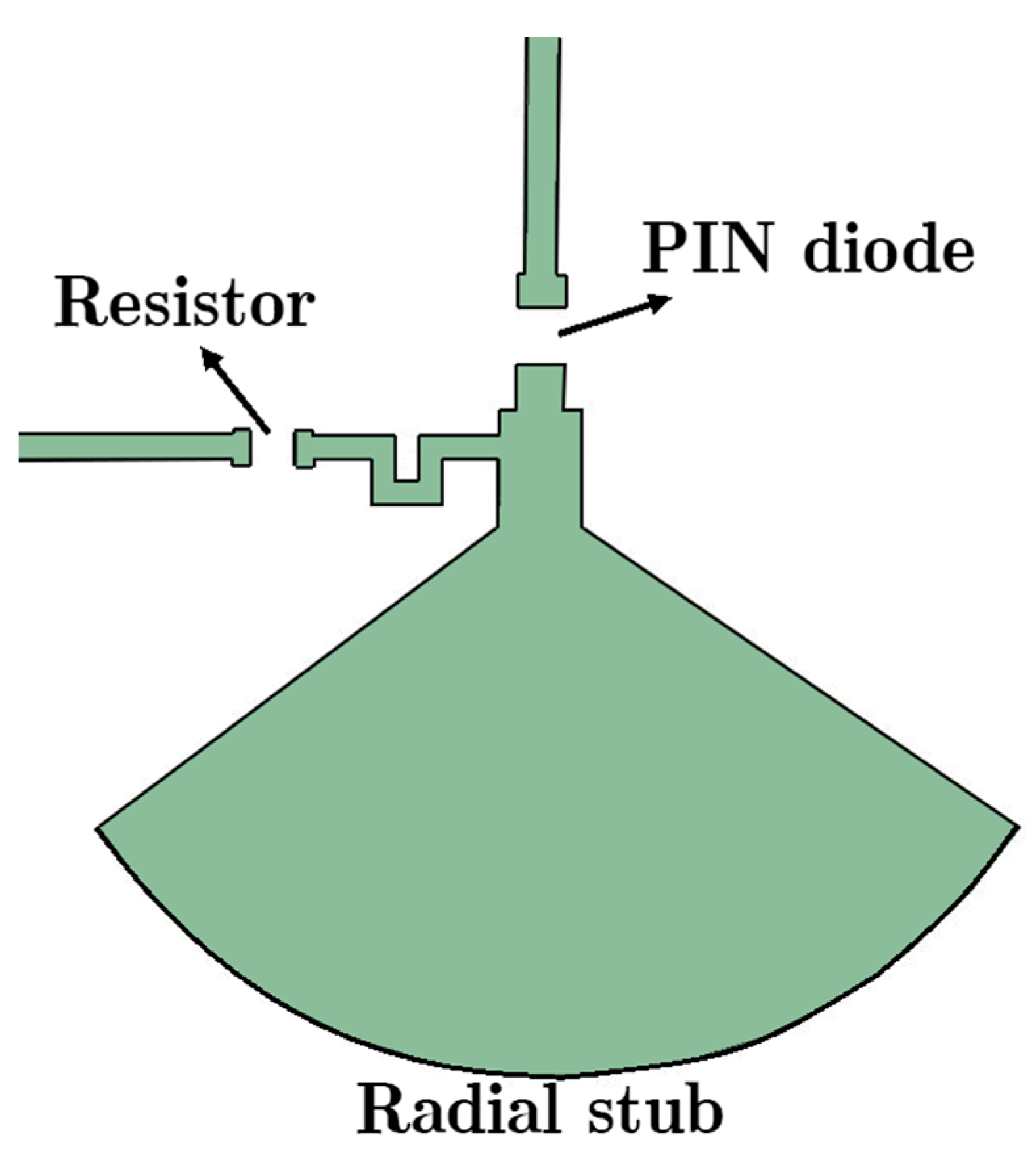
2.2. Phase Shifting Topology

A transmission line has its own fixed-phase feature. To change the phase of the transmitted signal, it is possible to integrate parallel posts with the fixed HM-SIW. As shown in Figure 2, three different microstrip lines with lengths P1, P2, and P3 are connected to the device. Three PIN diodes are added to the lines to change the load of the new integrated lines. Additionally, a 115 Ω resistor and a radial stub end are provided with L5 length and θ angle. The resistor, radial stub, and meander line after the PIN diode function as a DC/RF blockage. To reduce the requirement for additional technology in the design, this isolation technique is implemented on the same layer as the RF phase shifter.
Depending on the DC bias support of PIN diodes, their situation may change (voltage > 0.8 V). To block interference between the two sources, the DC/RF isolating technique is implemented (Figure 3 illustrates this technique). To generate a broad resonant RF short circuit, a radial stub is used (L5 = 4.61 mm and θ ≈ 110°). It can provide a decoupling network between one source and other components. Furthermore, PIN diodes must be modeled in order to be exploited in numerical software. The electronic circuit model of a PIN diode is shown in Figure 4. A parallel RLC circuit is applied instead of a PIN diode element for the HM-SIW, including both diode states. During the ON state, it can be a parallel resistor or an inductance. On the other hand, it is a parallel capacitor and resistor in the OFF state. The diode is modeled as a low-value resistor in the ON state. In contrast, it is a high-value resistor when it is in the OFF state. A parallel RLC circuit model is exploited because some simulation software, such as ANSYS HFSS, is only able to consider parallel RLC elements.
The PIN diode is MPP4201 from Microsemi, and the resistor is from KOA Speer Electronics. The required voltage for changing the diode situation to an ON state was 0.8 V. For the linear performance of the diode, a stable DC voltage source with the desired switch is used.

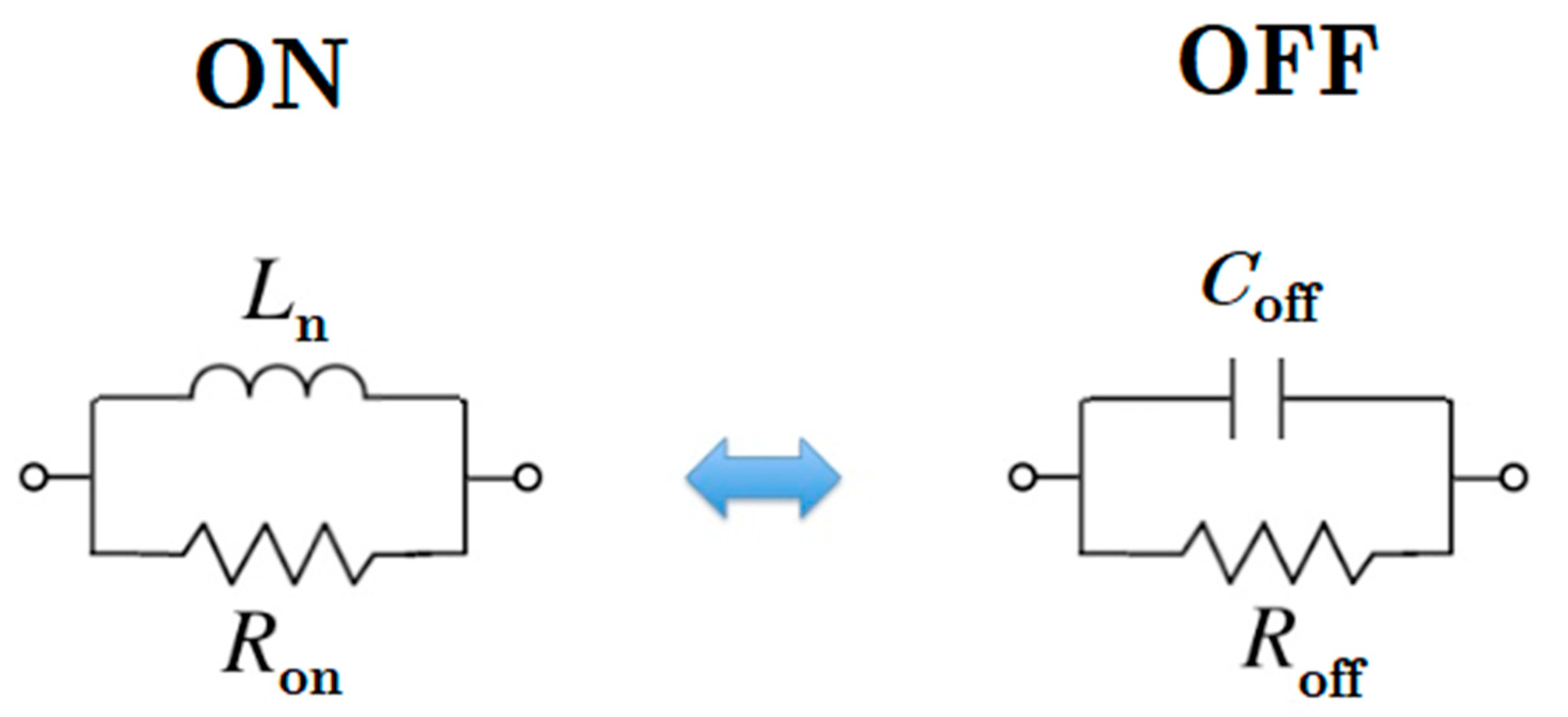
2.3. Working Principle

This subsection provides a qualitative perspective on the principle of structure. One method to analyze the structure is to hypothesize HM-SIW as a transmission line [45]. Despite being a high-pass filter by considering the cut-off frequency, the HM-SIW’s primary mode reduces signal transmission to a band-pass. The equivalent circuit element of a high-pass filter with one parallel stub is modeled as a T-network high-pass filter circuit in Figure 5 [24,30]. By adding inductance to the parallel branch, it is possible to increase the phase shift when compared with the reference value. This procedure is applied in the schematic of Figure 6. The lumped element values for the high-pass filter are from an equivalent value for a Butterworth model [46]. Then diode post values can tune both the phase and amplitude values of the reference HM-SIW. This principle is applied here for phase shifting applications with parametric studies, simulation software, and concrete measurement.
When looking at Figure 2, the added length of lines connecting to the PIN diodes presents a constant phase shift for every branch. Additionally, they provide enough space for a diode soldering pad. The location of PIN diode stubs is tuned with full wave simulation, considering fabrication constraints and achieving a sensible phase shift for a smaller total length.

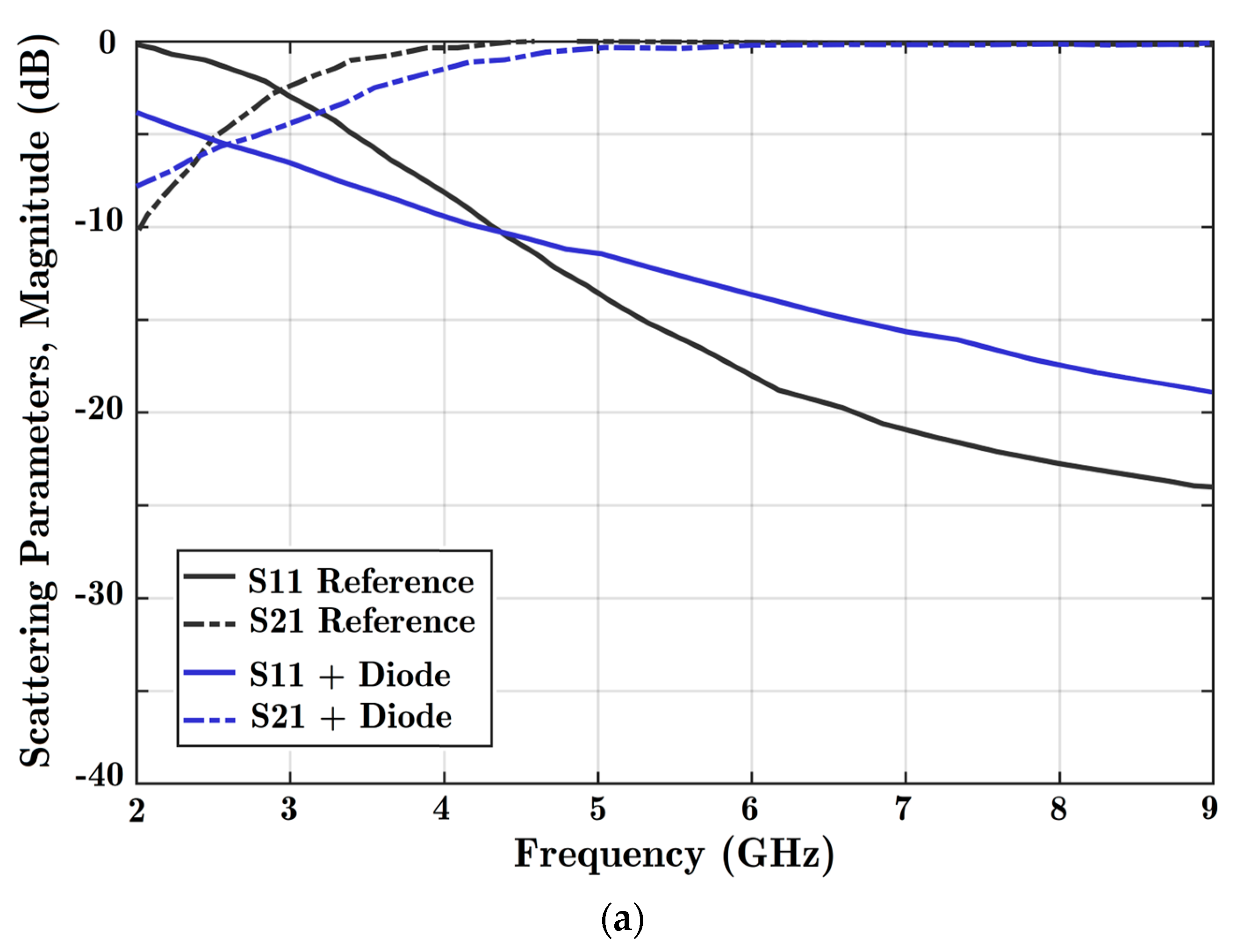
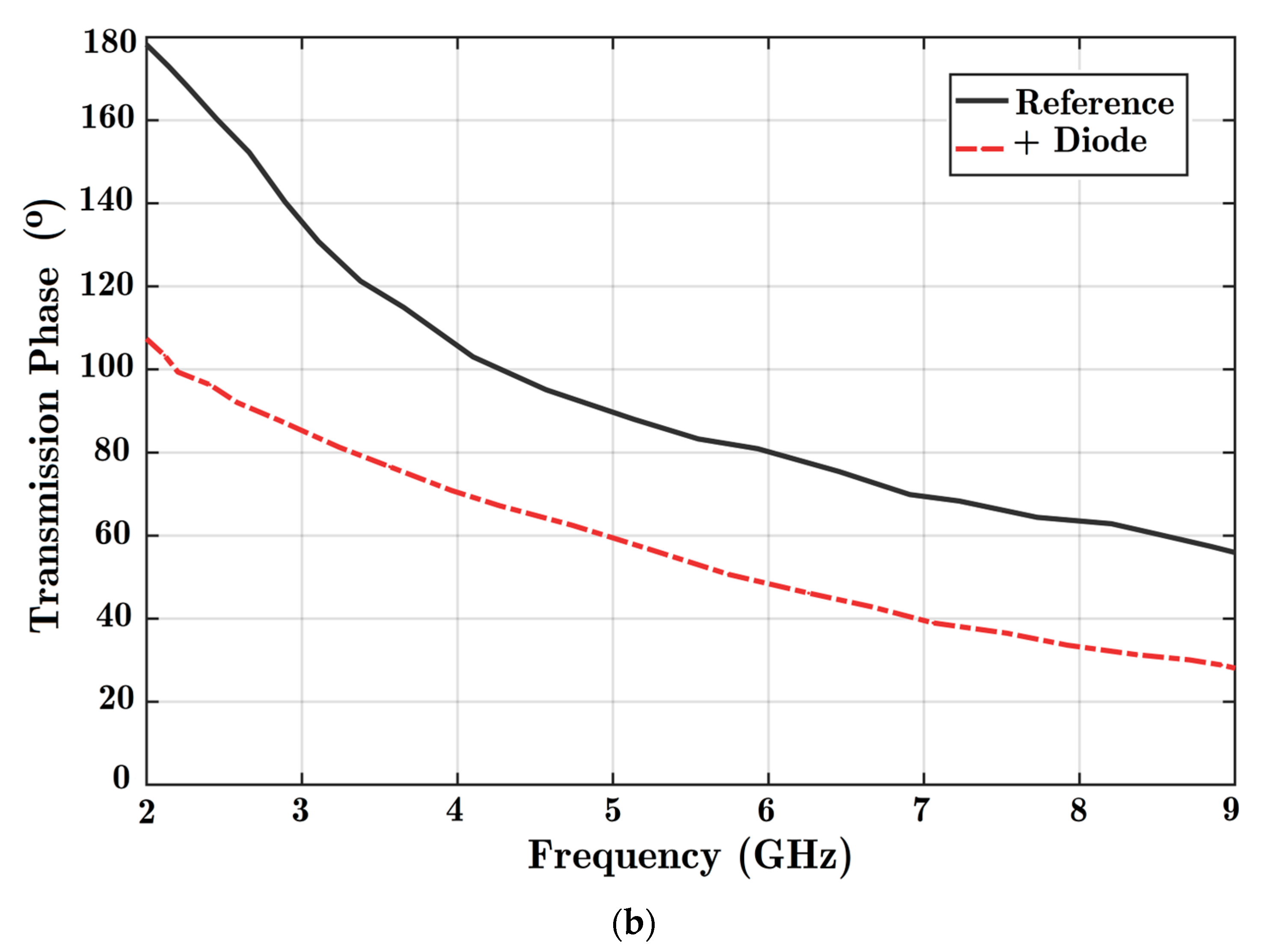
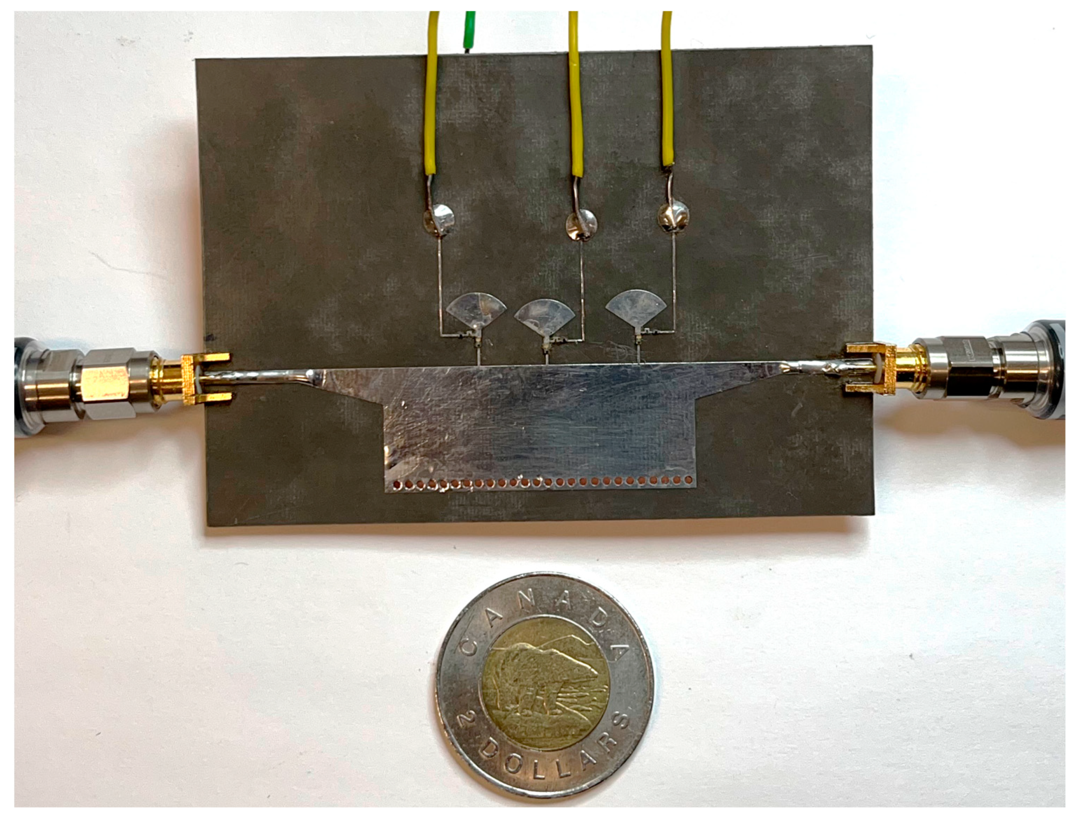
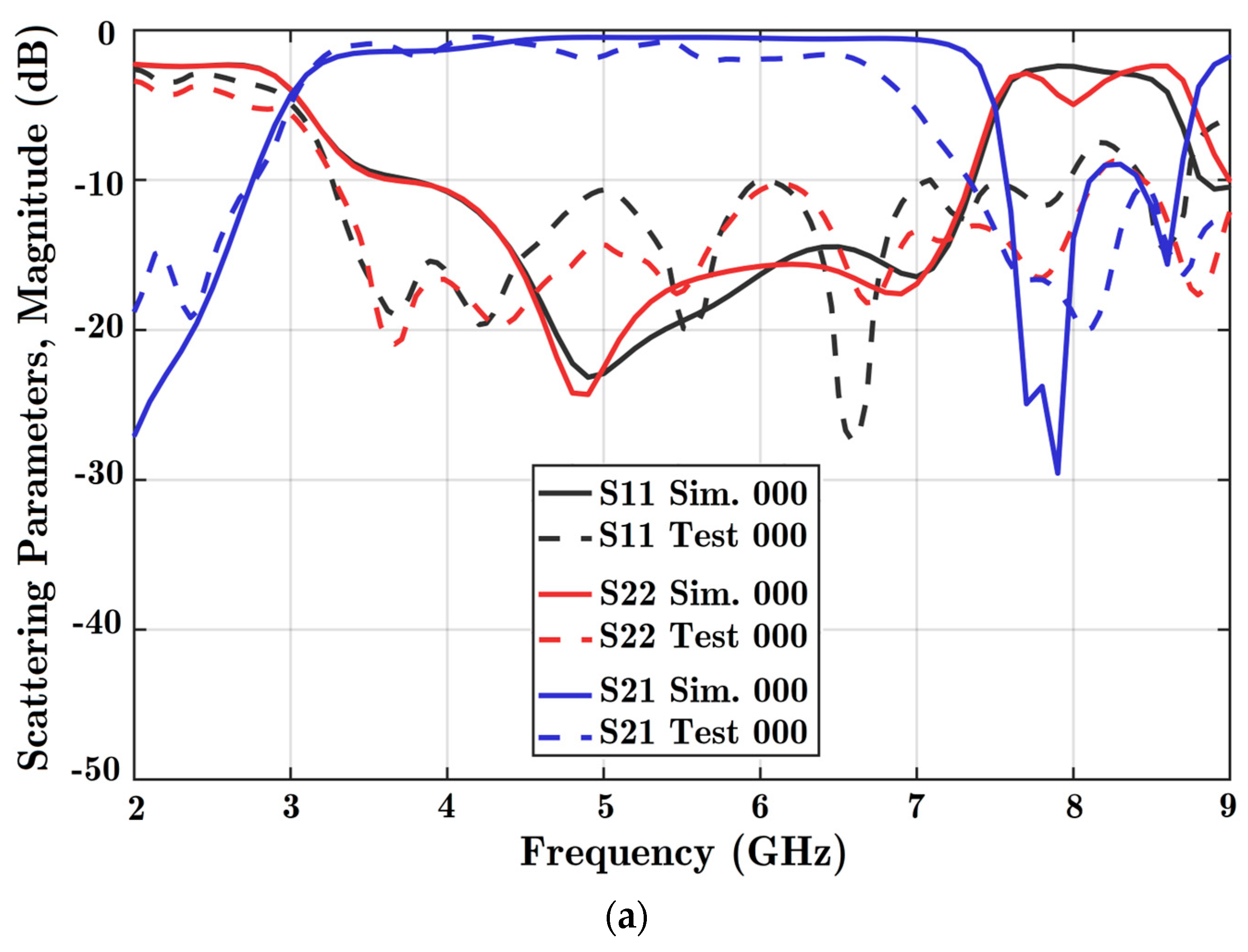
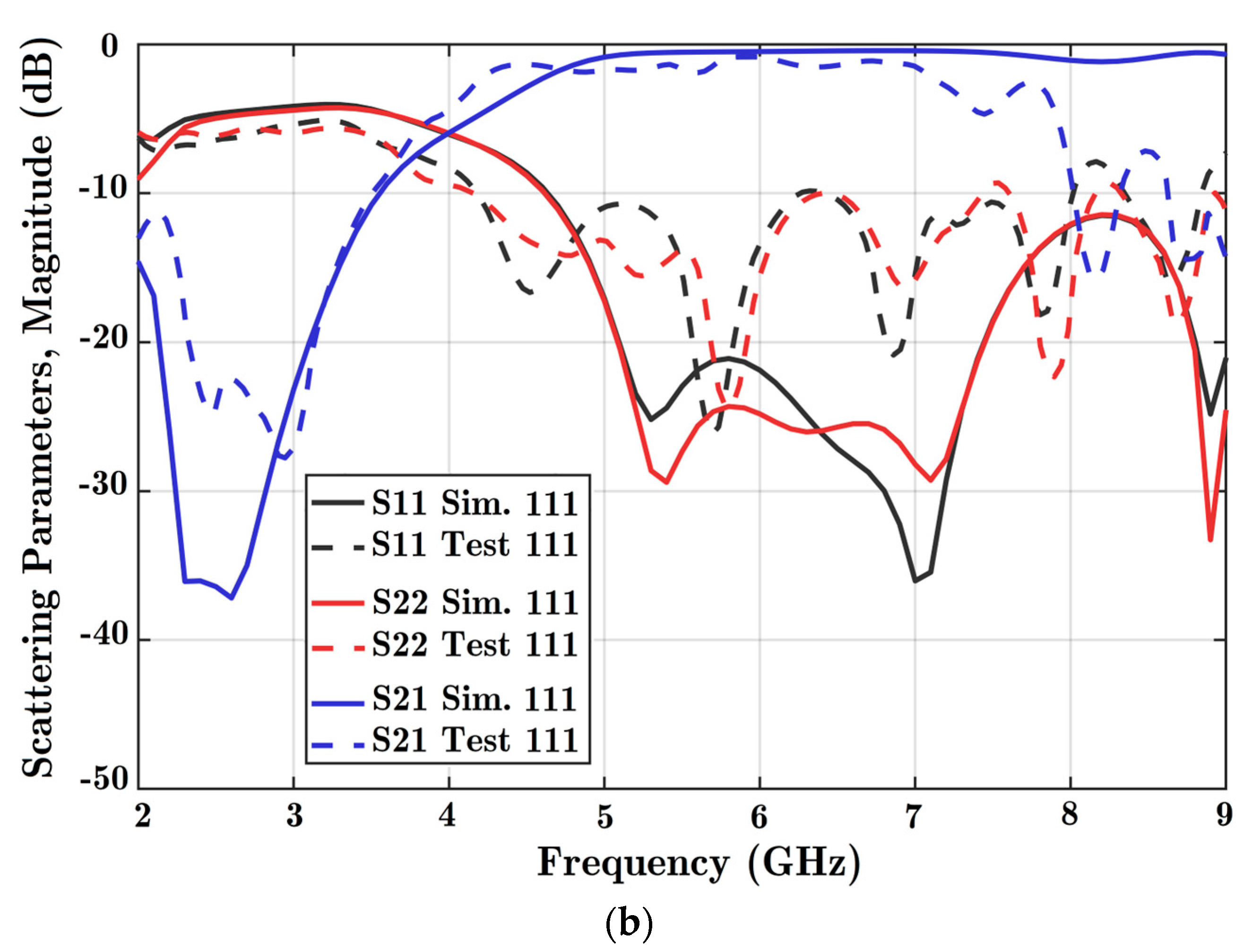
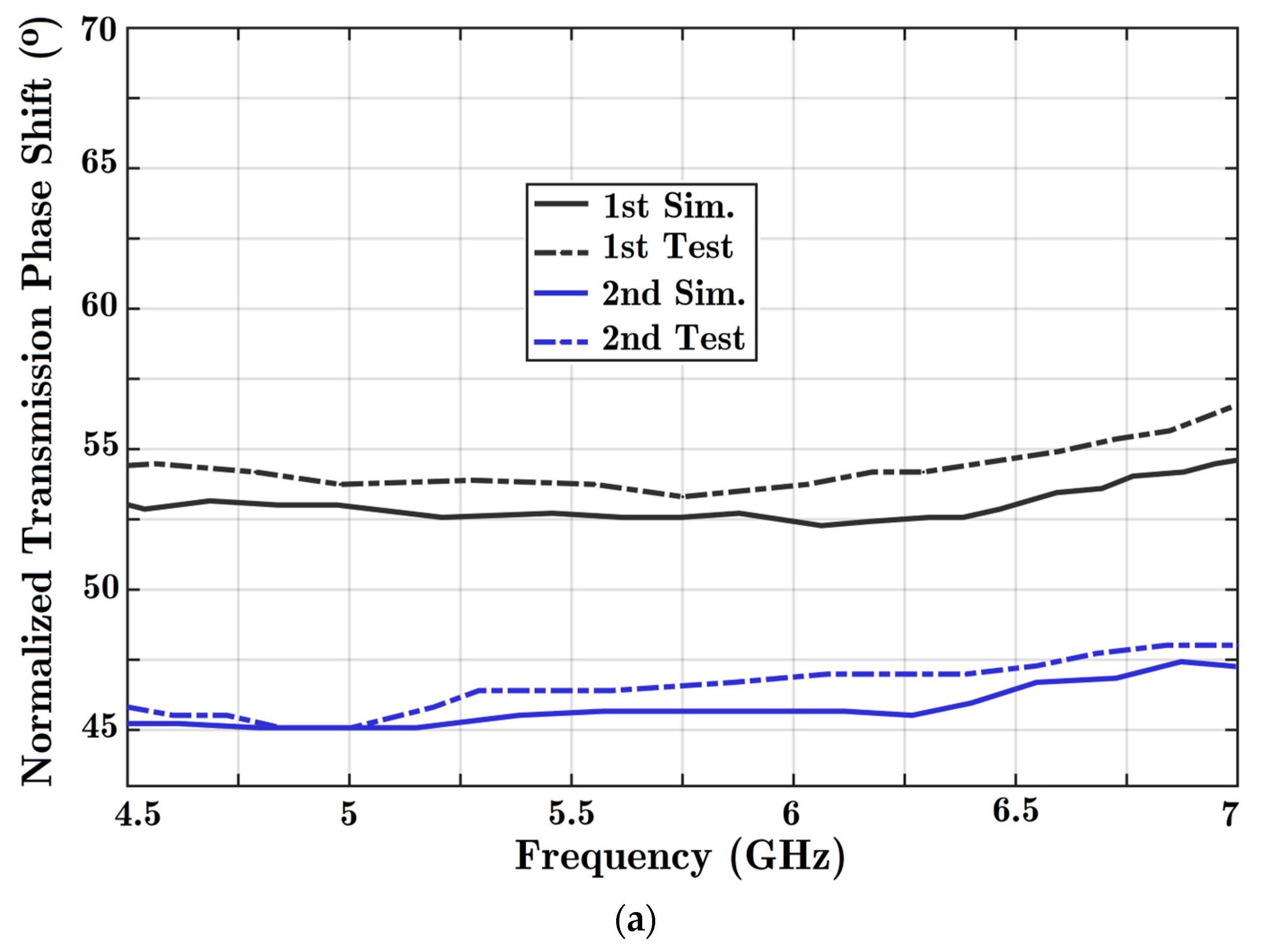
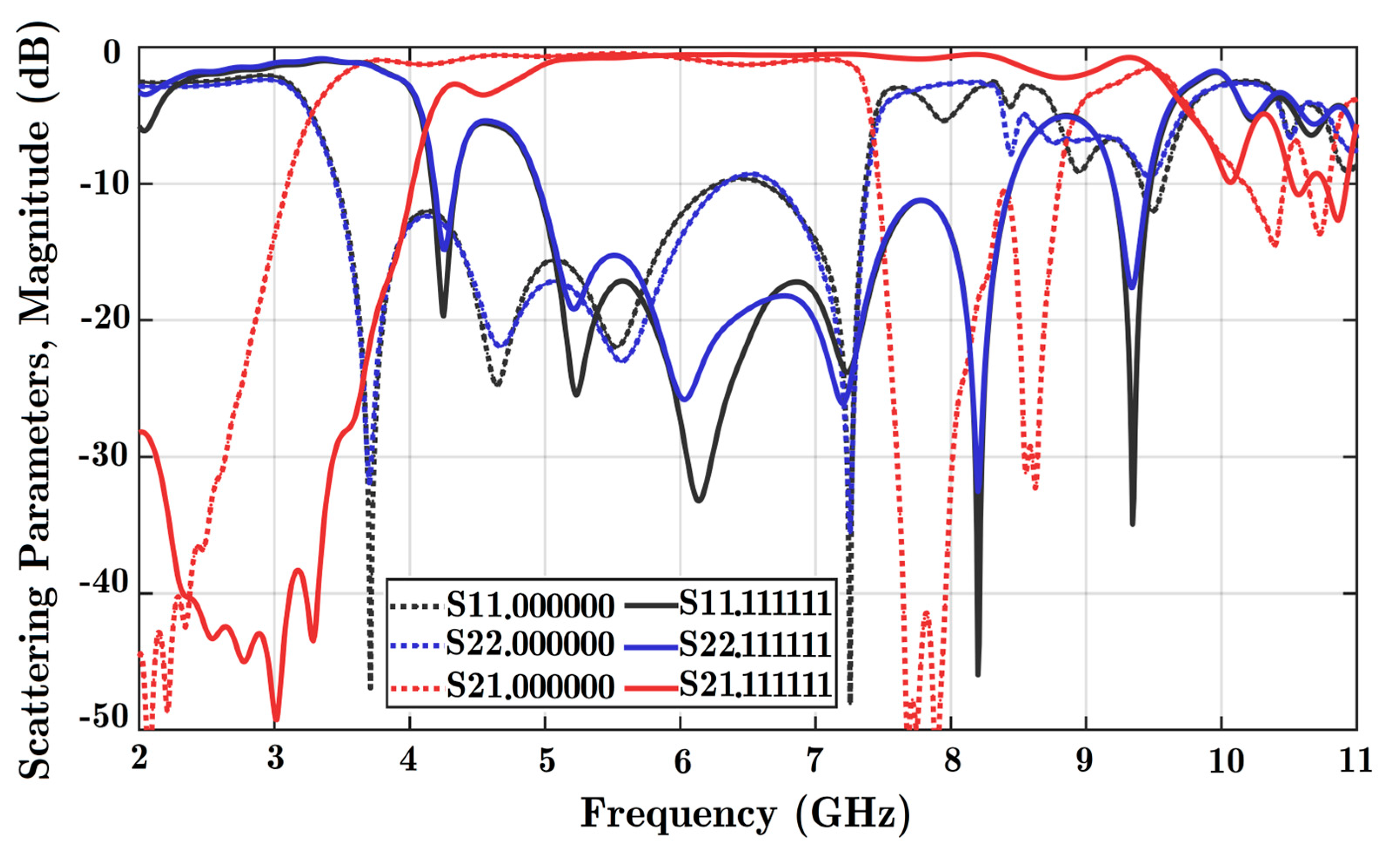
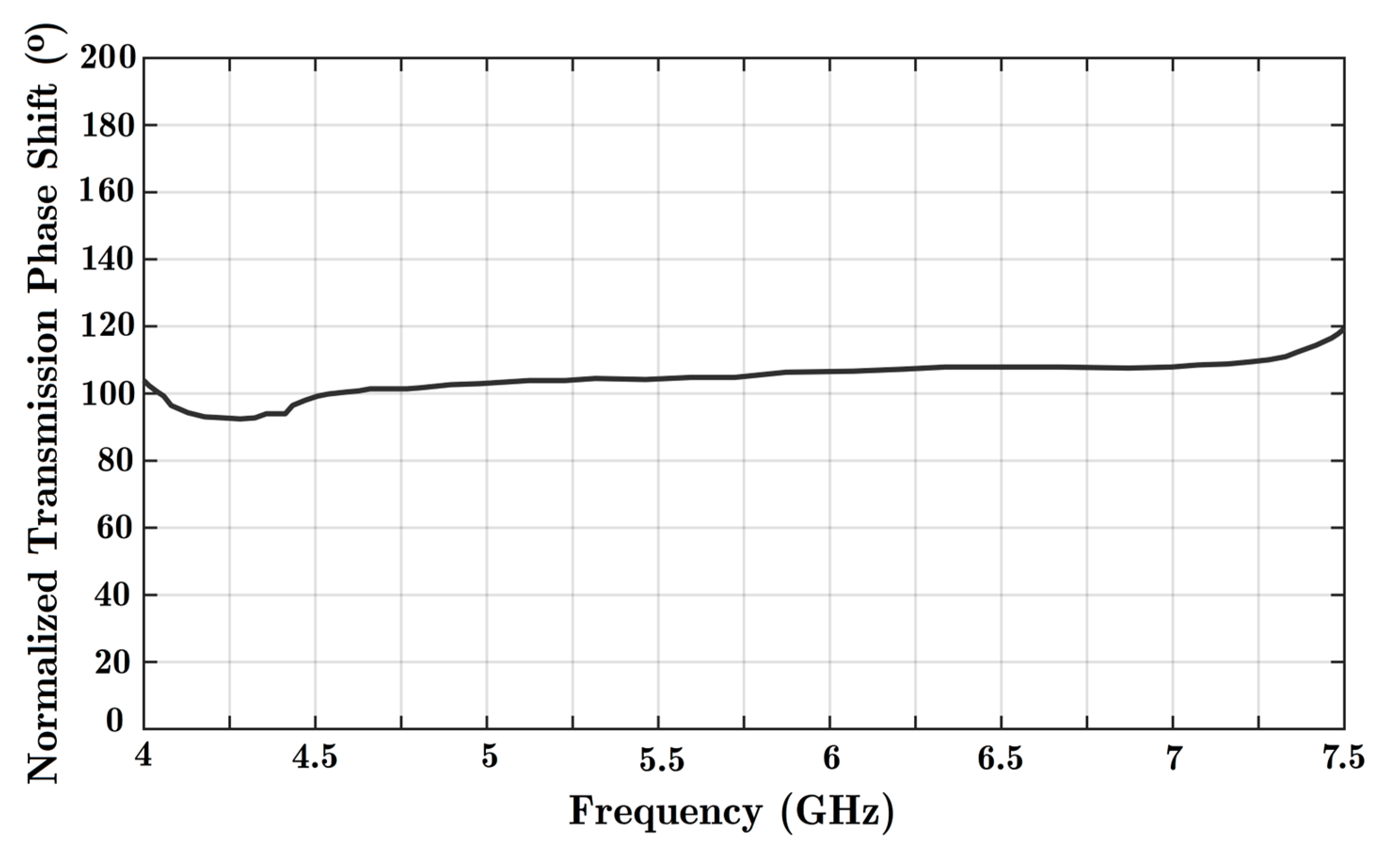
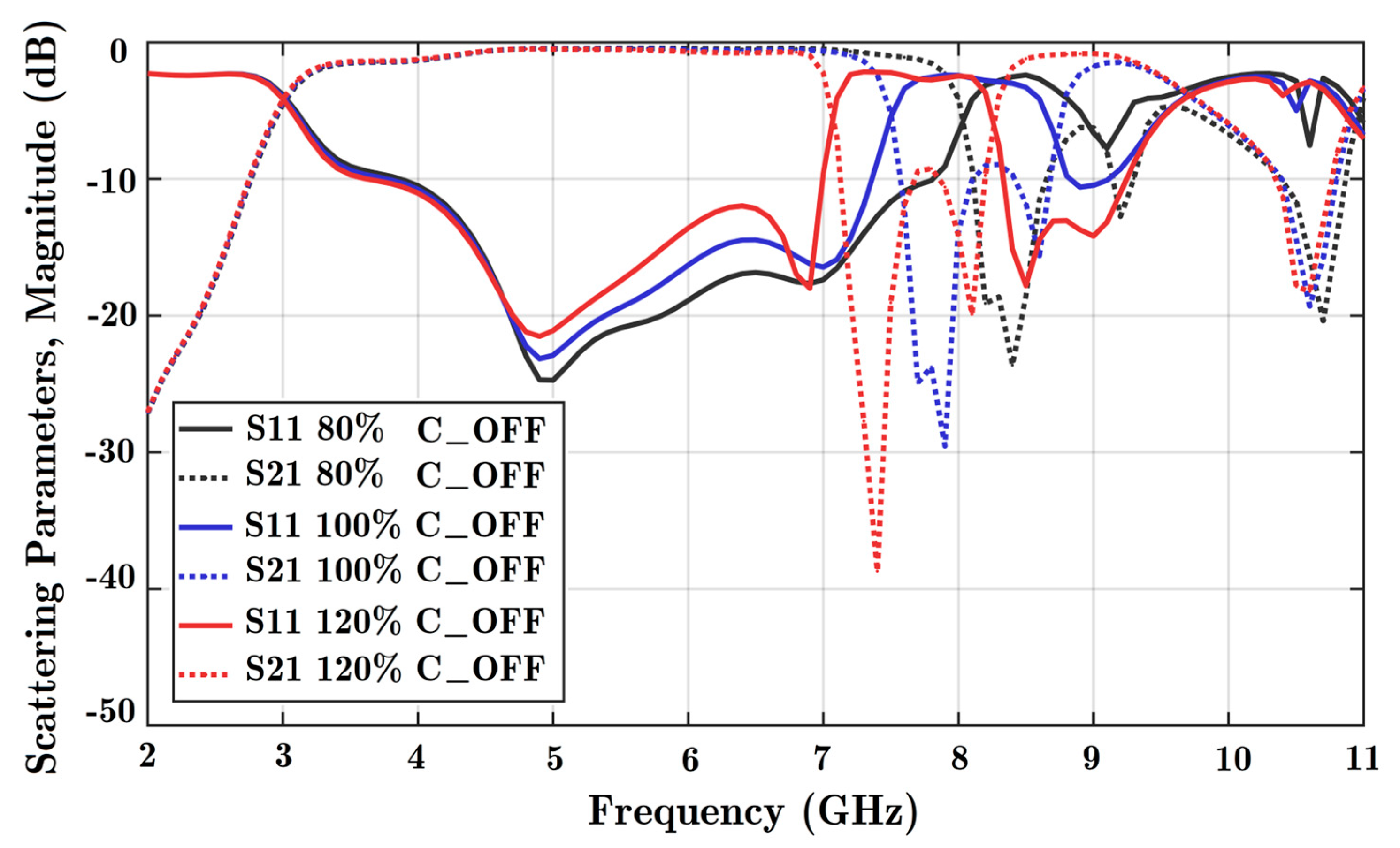
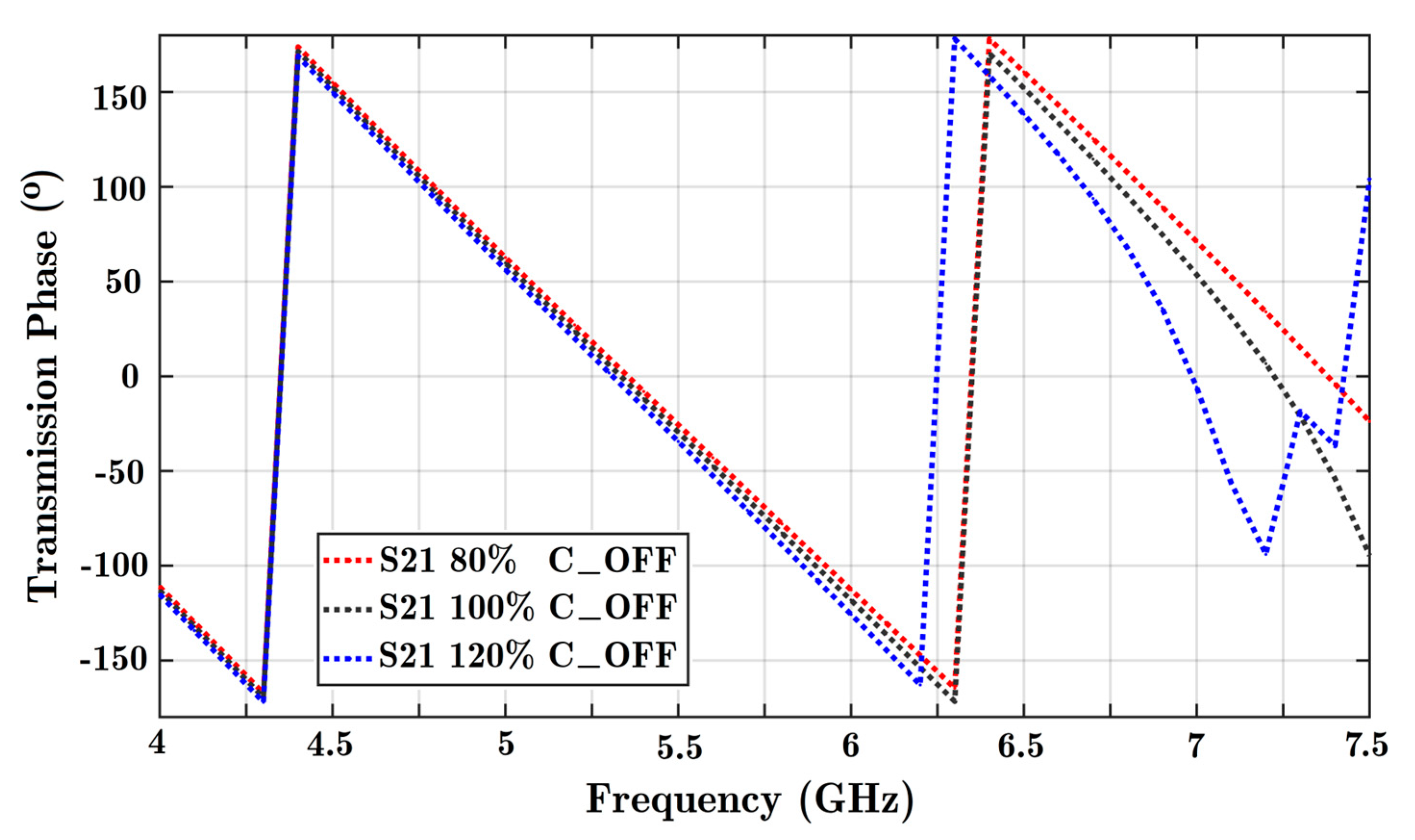
3. Results and Discussion of Varied Solutions

The proposed structure was designed in numerical full wave simulation software according to the geometry of Figure 2. In light of the scattering parameters, the geometry was tuned to provide suitable performance across the frequency range. The background surface is applied with a perfect electric conductor as the boundary condition. Other directions are chosen as open added-space boundaries. Two ideal waveguide ports with larger areas are added to the two microstrip lines at the corners. The frequency of analysis in the simulation software is 2 to 9 GHz. Various simulation software, including CST, ANSYS HFSS, and a circuit analyzer (ADS), is used to verify the structure before a concrete measurement study.
To further evaluate a HM-SIW phase shifter microwave component, the proposed structure is fabricated as shown in Figure 7. Two SMA connectors are soldered to the input and output ports. In the figure, the metallic surface of the HM-SIW is covered with copper and solder paste. A portable network analyzer from Keysight (N9950B) is connected to investigate the scattering parameters for two ports, including reflection and coupling values both in dB and phase units. Before performing the scattering parameter measurements, a mechanical 2-port calibration is conducted (based on a broadband SOLT kit). PIN diodes and resistors are soldered to the board. Then, a DC source is employed to change the diode situation using key control. For better soldering on the same SIW surface, three extra arms connected in one direction to the diode are provided. On the opposite side of the background, the diodes are connected to a DC source in the other direction.
There are three diodes in the design; therefore, eight different formations of diode states can be explored. The first state, 000, shows that all three diodes are OFF. Moreover, 111 indicates that all three diodes are in the ON state. The magnitude of scattering parameters in dB is obtained in these two situations from varied solutions. In Figure 8, the scattering coefficients for both ports are acceptable from 4.5 to 7 GHz for both scenarios. Based on the different solutions, the reflection coefficients of both ports were below −10 dB, and the coupling parameter was below −2 dB considering the assigned frequency band. The coupling parameter was not acceptable to work at frequencies exceeding 7 GHz in the experiment because of loss in the connectors.
Once proper wave transmission has been carried out in the allocated frequency band, both solutions are examined to determine the phase of transmission. Since three PIN diodes are integrated in the transmission line, there would be eight different situations for diodes. State 000 assigns the first and reference situations. Then, by changing the states of the diodes one by one, the transmission phase variation is analyzed. The phase variation can be controlled digitally with this reconfigurable phase shifter. Figure 9 presents the phase difference resulting from normalizing different diode states to the reference 000 formation.
A maximum 55° phase shift is achieved when all diodes are ON (as shown in Figure 9a). For the entire frequency range, a nearly stable response is achieved. Moreover, different diode formations lead to a quantitative feature in the phase shifter. Only phase shift performance in the 4.5 to 7 GHz frequency range is shown in the charts.
Ideally, phase shifters should provide a constant phase shift and dominant signal transmission. The signal coupling parameter in Figure 8 shows high quality wave transmission. In addition, a nearly constant phase difference is achieved based on the analysis of Figure 9, considering every frequency point.
In order to compare the achieved results with similar phase shifter designs in the literature, Table 1 was prepared. The proposed structure has a promising configuration compared to recent phase shifter designs in the literature. In addition to the tunable states (seven normalized modes), the DC biasing of PIN diodes is integrated into a similar layer as the RF signal. This feature eliminates the need for an extra bias layer (preventing multilayer designs). Furthermore, the half-mode design decreases the width of the SIW phase shifter, which makes it an ideal device for modular and integrated systems. Miniaturized size and enhanced DC biasing technology enable a reliable, cost-effective electronic component that can be integrated into a package. As an example, the proposed system can be applied to a sensing antenna for the phase engineering section. Beam steering systems require compact phase shifters. With a phase shifter, it is possible to realize a high-resolution detective system for applications such as automatic radar sensors. Another application of this innovative phase shifter is for time-varying surfaces.
Furthermore, a revised model is simulated using simulation software in Appendix A to illustrate the capabilities of the proposed HM-SIW structure. It is possible to cascade two or more phase shifters to generate higher phase shift values. Signal loss happens at port connections and transitions, so cascading more phase shifter components does not generate more loss. This expanded design is included in Appendix A of the simulation software. The total size of the redesigned model will increase by 41%.
Moreover, a parametric study is provided in Appendix B. The parametric study covers the nonlinearity and variation of PIN diode characteristics, including the equivalent parallel circuit models. In this case, the diode parameters such as resistance, inductance, and capacitance were tuned to further investigate their effects on the scattering parameters of the HM-SIW. As well as using full wave simulation software to analyze the compact structure, circuit simulation software is used to study the different circuit elements modeling the diodes.

4. Conclusions

A brand-new half-mode substrate integrated waveguide (HM-SIW) phase shifter is proposed here to cover 4.5 to 7 GHz frequencies. The structure is based on microstrip lines integrated into HM-SIW, PIN diodes, and radial stubs. It is optimized to achieve low insertion (<−2 dB) and reflection losses. By exploiting a half-mode SIW formation, it results in a smaller dimension than a typical SIW formation. A parametric study achieves high performance with multiple phase shifts, scattering parameters, and a miniaturized modular design. The primary design concept covers 0° to 60° phase shifts with 7 distinct states. By cascading two similar topologies without extra wave dissipation, the phase shift can reach 120°. Furthermore, the observed phase deviation was less than 5° in the frequency band. The structure is innovatively designed on one substrate layer. This makes it compact, low-loss, and low-profile, so it can be easily combined with other modular microwave devices. It does not require extra wire binding for DC biasing the tunable element (PIN diode). This makes it attractive for millimeter-wave frequencies and applications such as sensing and antenna beamforming.

Author Contributions

Conceptualization, H.B. and F.D.W.; methodology, H.B. and F.D.W.; software, A.G., B.M. and F.D.W.; validation, H.B., A.G. and F.D.W.; resources, H.B. and L.T.; writing—original draft preparation, B.M. and F.D.W.; writing—review and editing, H.B. and A.G.; supervision, H.B. and L.T. All authors have read and agreed to the published version of the manuscript.

Funding

This research received no external funding.

Informed Consent Statement

Not applicable.

Data Availability Statement

The data presented in this study are openly available.

Conflicts of Interest

The authors declare no conflict of interest.

Abbreviations

In order to help readers, some key terms and symbols are described in this part as follows.
SIWSubstrate integrated waveguide
HM-SIWHalf-mode substrate integrated waveguide
RFRadio frequency
RLCResistor, inductance, capacitance
SOLTShort, open, load, through
CST, ANSYS HFSS, AWR, and ADS are different simulation software

Appendix A

It should be noted that all diode states can prepare for a phase shift from 15° to 55°. More phase shift is possible by cascading the structures without extra loss in the wave transition. The main dissipation in the signal is from the microstrip to SIW transition, including the port matching mechanism. This appendix provides a cascaded structure similar to the proposed design. For this study, simulation software is used only to elaborate on the capabilities of a HM-SIW phase shifter. The updated structure has a length of Lnew = 73 mm, as illustrated in Figure A1.
Figure A1. A proposal for cascading the structure of the phase shifter with the HM-SIW to generate twice the primary phase shifts.
Technologies 11 00063 g0a1
It is achieved that the operating frequency of this cascaded phase shifter is 4.8 to 7.4 GHz for the extended design. It is the result of a simple transforming property of the design of the structure without additional geometric optimization in the simulation medium. In CST software, only a copy-transfer operation is utilized to create a simple extended feature for this purpose. With proper tuning of the cascaded structure, it is possible to achieve a similar frequency band. Scattering parameters are shown in Figure A2 for both reflection and coupling coefficients. Only two scenarios, all diodes OFF and all diodes ON, are considered here for the sake of brevity. Within the assigned frequency bandwidth, the coupling value was less than −2 dB, and the reflection coefficient of the two ports was less than −10 dB.
Figure A2. Scattering parameters versus frequency for two states: all diodes OFF, and all diodes ON. Reflection coefficients for port 1 (S11), port 2 (S22), and the coupling parameter between the ports (S21) are obtained. Only simulation software is executed for this cascaded phase shifter element. State 000000 is the situation with all diodes OFF (dotted lines), while 111111 represents six diodes ON at the same time (solid lines).
Technologies 11 00063 g0a2
A similar diode feature is added to the design. Moreover, the number of diodes has increased to six in this extended design. The purpose of a cascaded phase shifter based on the proposed HM-SIW is to show the capability of the microwave device to achieve higher phase shifts. The increased number of diodes also leads to more phase shifts. As shown in Figure A3, the extended structure achieved the maximum value of phase shift. Now, it is possible to have up to 120° of phase shift. By cascading three phase shifters, the ultimate transmission phase shift value would be 180°.
Figure A3. The maximum achieved phase shift value is presented using an extended reconfigurable structure with six diode posts integrated with a HM-SIW transmission line.
Technologies 11 00063 g0a3

Appendix B

As PIN diodes are nonlinear elements, their equivalent circuit models can be varied by altering the supply voltage and bias source [47]. It is possible to use a precise DC source and a fast switch key to change the state of a PIN diode with more consistency. As another option, the proposed phase shifter can be applied in a receiving section using a lower amount of RF power signal (a small signal). This will improve the stability of the diode.
A parametric analysis was performed here with the purpose of applying a 20% variation to some equivalent circuits of the applied PIN diode in simulation software. The components to be studied are the resistor and inductance values in the ON state and the capacitance in the OFF state (Coff = 0.10704, 0.1338, and 0.16056 PF).
To perform parametric studies, it is beneficial to use circuit software, such as ADS or AWR, rather than working with full-wave CST or ANSYS HFSS. This is because circuit software is here to tune equivalent circuit elements. First, the structure is simulated without PIN diodes in CST. To replace the diode component, discrete ports are added that connect to the ground layer. Then, there would be eight different ports, including the two main input and output ports in the case of the proposed fabricated structure. In the next step, scattering parameters can be exported in s8p format with a normalized 50 Ω impedance. Then a s8p file can be applied to an 8-port scattering module in ADS software. Finally, it is an easy and quick way to tune the equivalent parameters of the diode in circuit software to achieve the desired scattering parameters.
Figure A4 is the parametric study for the OFF state on the scattering parameters. Similarly, Figure A5 presents the variation of the OFF state capacitance in the transmission phase. Changing the ON state parameters does not affect either the magnitude or phase of the scattering parameters in a sensible way.
Figure A4. Scattering parameters versus frequency for parametric studies when all diodes are OFF. Reflection coefficients for port 1 (S11) and the coupling parameter between the ports (S21) are obtained. Only simulation software was used for these parametric studies. Dotted lines indicate coupling, while solid lines represent reflection coefficients (80% C = 0.10704, 100% C = 0.1338, and 120% C = 0.16056 PF).
Technologies 11 00063 g0a4
Figure A5. Variation of the transmission phase using different capacitance parameters in the off state. Changes in the transmission phase are noticeable at higher frequencies. A frequency range of 4 to 7.5 GHz is considered here.
Technologies 11 00063 g0a5
The parametric analysis shows that with a lower-capacitance PIN diode, it is possible to increase the operating frequency band of the phase shifter.

References

  1. Schiffman, B.M. A new class of broad-band microwave 90-degree phase shifters. IRE Trans. Microw. Theory Tech. 1958, 6, 232–237. [Google Scholar] [CrossRef]
  2. Qiu, L.-L.; Zhu, L.; Ouyang, Z.-A.; Deng, L. Wideband Butler matrix based on dual-layer HMSIW for enhanced miniaturization. IEEE Microw. Wirel. Compon. Lett. 2021, 32, 25–28. [Google Scholar] [CrossRef]
  3. Akbari, M.; Farahani, M.; Ghayekhloo, A.; Zarbakhsh, S.; Sebak, A.-R.; Denidni, T.A. Beam tilting approaches based on phase gradient surface for mmWave antennas. IEEE Trans. Antennas Propag. 2020, 68, 4372–4385. [Google Scholar] [CrossRef]
  4. Guo, Y.-X.; Zhang, Z.-Y.; Ong, L.C. Improved wide-band Schiffman phase shifter. IEEE Trans. Microw. Theory Tech. 2006, 54, 1196–1200. [Google Scholar] [CrossRef]
  5. Rohaninezhad, M.; Ghayekhloo, A.; Afsahi, M.; Denidni, T.A. Design of a Transparent System for Mutual Coupling Reduction of Microstrip Array Antennas with Confined Water. Phys. Status Solidi (a) 2022, 219, 2200082. [Google Scholar] [CrossRef]
  6. Ghayekhloo, A.; Akbari, M.; Afsahi, M.; Orouji, A.A.; Sebak, A.R.; Denidni, T.A. Multifunctional transparent electromagnetic surface based on solar cell for backscattering reduction. IEEE Trans. Antennas Propag. 2019, 67, 4302–4306. [Google Scholar] [CrossRef]
  7. Zarbakhsh, S.; Sebak, A.R. Multifunctional Drone-Based Antenna for Satellite Communication. IEEE Trans. Antennas Propag. 2022, 70, 7223–7227. [Google Scholar] [CrossRef]
  8. Omam, Z.R.; Abdel-Wahab, W.M.; Raeesi, A.; Palizban, A.; Pourziad, A.; Nikmehr, S.; Gigoyan, S.; Safavi-Naeini, S. Ka-band passive phased-array antenna with substrate integrated waveguide tunable phase shifter. IEEE Trans. Antennas Propag. 2020, 68, 6039–6048. [Google Scholar] [CrossRef]
  9. Kim, D.-C.; Park, S.-J.; Kim, T.-W.; Minz, L.; Park, S.-O. Fully digital beamforming receiver with a real-time calibration for 5G mobile communication. IEEE Trans. Antennas Propag. 2019, 67, 3809–3819. [Google Scholar] [CrossRef]
  10. Louati, S.; Talbi, L.; Hettak, K.; Boutayeb, H. 28 GHz Digital SIW Phase Shifter Using Embedded PIN Diodes. In Proceedings of the IEEE International Symposium on Antennas and Propagation and USNC-URSI Radio Science Meeting (AP-S/URSI), Denver, CO, USA, 10–15 July 2022; pp. 848–849. [Google Scholar] [CrossRef]
  11. Ghayekhloo, A.; Boutayeb, H.; Talbi, L. Developing an Electromagnetic Vortex Beam Structure Based on Advanced Plasma Transmit-array. In Proceedings of the IEEE International Symposium on Antennas and Propagation and USNC-URSI Radio Science Meeting (AP-S/URSI), Denver, CO, USA, 10–15 July 2022; pp. 740–741. [Google Scholar] [CrossRef]
  12. Khodaee, M.; Akbari, M.; Zarbakhsh, S. A Novel Antenna with Dual Band-Notched Characteristics using Shorting Pin and Z-Shaped Slot on Conductor Backed. Appl. Comput. Electromagn. Soc. J. ACES 2013, 28, 809–814. [Google Scholar]
  13. Akbari, M.; Khodaee, M.; Zarbakhsh, S.; Gholami, R. A simple UWB antenna with dual stop-band performance using rectangular slot and strip line ended up shorting pin. Prog. Electromagn. Res. C 2013, 42, 83–94. [Google Scholar] [CrossRef]
  14. Ali, Q.; Shahzad, W.; Ahmad, I.; Safiq, S.; Bin, X.; Abbas, S.M.; Sun, H. Recent developments and challenges on beam steering characteristics of reconfigurable Transmitarray antennas. Electronics 2022, 11, 587. [Google Scholar] [CrossRef]
  15. Parment, F.; Ghiotto, A.; Vuong, T.-P.; Duchamp, J.-M.; Wu, K. Double dielectric slab-loaded air-filled SIW phase shifters for high-performance millimeter-wave integration. IEEE Trans. Microw. Theory Tech. 2016, 64, 2833–2842. [Google Scholar] [CrossRef]
  16. An, S.; Zheng, B.; Tang, H.; Li, H.; Zhou, L.; Dong, Y.; Haerinia, M.; Zhang, H. Ultrawideband Schiffman Phase Shifter Designed with Deep Neural Networks. IEEE Trans. Microw. Theory Tech. 2022, 70, 4694–4705. [Google Scholar] [CrossRef]
  17. Cano, J.L.; Mediavilla, A.; Tribak, A. Parametric design of a class of full-band waveguide differential phase shifters. Electronics 2019, 8, 346. [Google Scholar] [CrossRef]
  18. Shi, J.; Nie, Y.; Han, P.; Zhang, W.; Cao, Q. Compact filtering phase shifter with simple structure. IEEE Microw. Wirel. Compon. Lett. 2021, 31, 1263–1266. [Google Scholar] [CrossRef]
  19. Dong, Q.; Wu, Y.; Chen, W.; Yang, Y.; Wang, W. Single-layer dual-band bandwidth-enhanced filtering phase shifter with two different predetermined phase-shifting values. IEEE Trans. Circuits Syst. II Express Briefs 2020, 68, 236–240. [Google Scholar] [CrossRef]
  20. Zhu, X.; Yang, T.; Chi, P.-L.; Xu, R. Novel passive vector-sum reconfigurable filtering phase shifter with continuous phase-control and tunable center frequency. IEEE Trans. Microw. Theory Tech. 2021, 70, 1188–1197. [Google Scholar] [CrossRef]
  21. Wu, K.; Bozzi, M.; Fonseca, N.J.G. Substrate integrated transmission lines: Review and applications. IEEE J. Microw. 2021, 1, 345–363. [Google Scholar] [CrossRef]
  22. Hautcoeur, J.; Ghayekhloo, A.; Hettak, K.; Talbi, L.; Boutayeb, H.; Wu, K. 60 GHz Frequency Sensor Antenna for Short-Range Millimeter-Wave Detection Application. IEEE Sens. Lett. 2022, 6, 1–4. [Google Scholar] [CrossRef]
  23. Karami, F.; Boutayeb, H.; Amn-e-Elahi, A.; Ghayekhloo, A.; Talbi, L. Developing Broadband Microstrip Patch Antennas Fed by SIW Feeding Network for Spatially Low Cross-Polarization Situation. Sensors 2022, 22, 3268. [Google Scholar] [CrossRef]
  24. Sellal, K.; Talbi, L.; Denidni, T.A.; Lebel, J. Design and implementation of a substrate integrated waveguide phase shifter. IET Microw. Antennas Propag. 2008, 2, 194–199. [Google Scholar] [CrossRef]
  25. Muneer, B.; Qi, Z.; Shanjia, X. A broadband tunable multilayer substrate integrated waveguide phase shifter. IEEE Microw. Wirel. Compon. Lett. 2015, 25, 220–222. [Google Scholar] [CrossRef]
  26. Zhang, W.; Shen, Z.; Xu, K.; Shi, J. A compact wideband phase shifter using slotted substrate integrated waveguide. IEEE Microw. Wirel. Compon. Lett. 2019, 29, 767–770. [Google Scholar] [CrossRef]
  27. Omam, Z.R.; Abdel-Wahab, W.M.; Pourziad, A.; Nikmehr, S.; Palizban, A.; Gigoyan, S.; Safavi-Naeini, S. Tunable substrate integrated waveguide phase shifter using high dielectric constant slab. IEEE Microw. Wirel. Compon. Lett. 2020, 30, 485–488. [Google Scholar] [CrossRef]
  28. Ebrahimpouri, M.; Nikmehr, S.; Pourziad, A. Broadband compact SIW phase shifter using omega particles. IEEE Microw. Wirel. Compon. Lett. 2014, 24, 748–750. [Google Scholar] [CrossRef]
  29. Yang, T.; Ettorre, M.; Sauleau, R. Novel phase shifter design based on substrate-integrated-waveguide technology. IEEE Microw. Wirel. Compon. Lett. 2012, 22, 518–520. [Google Scholar] [CrossRef]
  30. Sellal, K.; Talbi, L.; Nedil, M. Design and implementation of a controllable phase shifter using substrate integrated waveguide. IET Microw. Antennas Propag. 2012, 6, 1090–1094. [Google Scholar] [CrossRef]
  31. Louati, S.; Boutayeb, H.; Hettak, K.; Talbi, L. New reconfigurable SIW phase shifter with transverse CPW-based stubs and PIN Diodes. In Proceedings of the IEEE International Symposium on Antennas and Propagation and USNC-URSI Radio Science Meeting (AP-S/URSI), Denver, CO, USA, 10–15 July 2022; pp. 850–851. [Google Scholar] [CrossRef]
  32. Boutayeb, H.; Zhai, W.; Repeta, M. Switchable lens antenna with integrated frequency selective structure. U.S. Patent 11,515,653, 29 November 2022. [Google Scholar]
  33. Wu, Z.; Shim, Y.; Rais-Zadeh, M. Miniaturized UWB filters integrated with tunable notch filters using a silicon-based integrated passive device technology. IEEE Trans. Microw. Theory Tech. 2012, 60, 518–527. [Google Scholar] [CrossRef]
  34. Nosrati, M.; Vahabisani, N.; Daneshmand, M. A novel ultra wideband (UWB) filter with double tunable notch-bands using MEMS capacitors. In Proceedings of the IEEE MTT-S International Microwave Symposium Digest (MTT), Seattle, WA, USA, 2–7 June 2013; pp. 1–3. [Google Scholar] [CrossRef]
  35. Shao, C.; Chu, H.; Zhu, X.-H.; Guo, Y.-X. Tunable Phase Shifter with Small Phase Error and Insertion Loss Fluctuation Using a Resonator-Based Structure. IEEE Trans. Circuits Syst. II Express Briefs 2022, 70, 11–15. [Google Scholar] [CrossRef]
  36. Dehbashi, R.; Oskouei, H.D.; Forooraghi, K. A novel broad-band microstrip radial stub resonator used in bias-T application. Microw. Opt. Technol. Lett. 2006, 48, 1766–1770. [Google Scholar] [CrossRef]
  37. Cheng, Y.; Hong, W.; Wu, K. Half mode substrate integrated waveguide (HMSIW) directional filter. IEEE Microw. Wirel. Compon. Lett. 2007, 17, 504–506. [Google Scholar] [CrossRef]
  38. Nguyen-Trong, N.; Fumeaux, C. Half-mode substrate-integrated waveguides and their applications for antenna technology: A review of the possibilities for antenna design. IEEE Antennas Propag. Mag. 2018, 60, 20–31. [Google Scholar] [CrossRef]
  39. Ho, M.-H.; Hsu, C.-I.G.; Tang, K.-H.; Hong, W. Miniaturized band pass filter design using half mode substrate integrated coaxial resonators. Micromachines 2022, 13, 389. [Google Scholar] [CrossRef] [PubMed]
  40. Fallah, M.; Ghayekhloo, A.; Abdolali, A. Design of frequency selective band stop shield using analytical method. J. Microw. Optoelectron. Electromagn. Appl. 2015, 14, 217–228. [Google Scholar] [CrossRef]
  41. Karami, F.; Rezaei, P.; Amn-e-Elahi, A.; Abolfathi, A.; Kishk, A.A. Broadband and efficient patch array antenna fed by substrate integrated waveguide feed network for Ku-band satellite applications. Int. J. RF Microw. Comput. Aided Eng. 2021, 31, e22772. [Google Scholar] [CrossRef]
  42. Karami, F.; Rezaei, P.; Amn-e-Elahi, A.; Abolfathi, A. An X-Band Substrate Integrated Waveguide Fed Patch Array Antenna: Overcoming low efficiency, narrow impedance bandwidth, and cross-polarization radiation challenges. IEEE Antennas Propag. Mag. 2021, 63, 25–32. [Google Scholar] [CrossRef]
  43. Wu, K.; Deslandes, D.; Cassivi, Y. The substrate integrated circuits-a new concept for high-frequency electronics and optoelectronics. In Proceedings of the 6th International Conference on Telecommunications in Modern Satellite, Cable and Broadcasting Service, Nis, Yugoslavia, 1–3 October 2003; pp. I–III. [Google Scholar] [CrossRef]
  44. Rayas-Sanchez, J.E.; Gutierrez-Ayala, V. A general EM-based design procedure for single-layer substrate integrated waveguide interconnects with microstrip transitions. In Proceedings of the IEEE MTT-S International Microwave Symposium Digest, Atlanta, GA, USA, 15–20 June 2008; pp. 983–986. [Google Scholar] [CrossRef]
  45. Shao, W.; Li, J.-L. Design of a half-mode SIW high-pass filter. Appl. Comput. Electromagn. Soc. J. ACES 2011, 26, 447–451. [Google Scholar]
  46. Bianchi, G.; Sorrentino, R. Electronic Filter Simulation & Design; McGraw Hill Professional: New York, NY, USA, 2007. [Google Scholar]
  47. Bidgoli, H.A.; Khodaei, M.; Tayarani, M. Multioctave Power Amplifier Design Using 9:1 Planar Impedance Transformer. IEEE Microw. Wirel. Compon. Lett. 2020, 31, 45–48. [Google Scholar] [CrossRef]
Figure 1. Schematic of the proposed HM-SIW structure from simulation software.
Technologies 11 00063 g001
Figure 2. Structure of the phase shifter with the HM-SIW including diode posts and RF/DC blocking system from simulation software (T1, T2, L2, L3, W2, W3, Wg, L, P1, P2, and P3 parameters are, respectively, 11.55, 8.55, 11, 12, 1.59, 4.7, 14.5, 40, 2.8, 1.8, and 2.8 mm).
Technologies 11 00063 g002
Figure 3. Specification of the PIN diode placement in the reconfigurable phase shifter design. The resistor is one element to isolate RF signals with DC bias.
Technologies 11 00063 g003
Figure 4. Equivalent circuit model of a PIN diode for two different states. Using a parallel arrangement for both states, the ON state is derived from a series-to-parallel transformation. (Ln = 0.209 nH, Ron = 33.3 Ω, Roff = 30 kΩ, and Coff = 0.1338 pF).
Technologies 11 00063 g004
Figure 5. Qualitative circuit model analysis of (a) a high-pass filter equaling the HM-SIW guided transmission line and (b) the effect of parallel impedance posts on the SIW topology (C1 = 1.061 pF and L1 = 1.326 nH). Port locations are shown in Figure 1. Furthermore, Figure 4 displays the values for the diode impedance (Z diode).
Technologies 11 00063 g005
Figure 6. Analysis of the effects of adding parallel stubs to the transmission line. Charts of (a) scattering parameter magnitudes and (b) transmission phase when the HM-SIW is alone (reference) and by adding a parallel diode (ON state) are prepared.
Technologies 11 00063 g006aTechnologies 11 00063 g006b
Figure 7. A fabricated HM-SIW phase shifter that can be easily integrated with other microwave components due to its compact, modular, and miniaturized features.
Technologies 11 00063 g007
Figure 8. Scattering parameters versus frequency for two states: (a) all diodes OFF, and (b) all diodes ON. Reflection coefficients for port 1 (S11), port 2 (S22), and the coupling parameter between the ports (S21) are obtained. Simulation software charts are in solid colors, and the experiment is shown in dashed lines. State 000 is the situation with all diodes OFF, while state 111 is three diodes ON at the same time.
Technologies 11 00063 g008aTechnologies 11 00063 g008b
Figure 9. The achieved phase shift quantities are presented using the proposed reconfigurable structure with three parallel diode posts integrated with a HM-SIW transmission line. Comparisons are made between the results of two concrete simulations and experiment solutions: (a) the first phase range of 45° to 70°; (b) the medium phase range of 30° to 45°; and (c) the primary phase steps of 0° to 30°.
Technologies 11 00063 g009aTechnologies 11 00063 g009b
Table 1. A comparison table with previously reported SIW phase shifter works and their performances.
References[20][24][25][26][27][28][29][30][35]This Work
TechnologyTwo
reconfigurable filter couplers
Change in
the diameter
and position
of posts
Change
length
of slots
Two slots
location
Control the
distance of a high
dielectric
constant
Different cross-sectional elementsChange in the
position
of posts
Change the
waveguide
loading
Tunable resonators with varactorParallel
embedded
component with HM-SIW
Frequency (GHz)1–1.31010–142629–314.2–7.222.5–26.59.5–10.56.54.5–7
Phase
difference (°)
3005590 and
180
−90, −45, 0, 45, 9027545 and 906045360~60
Insertion loss (dB)−4−1−1.5−1.5−2−2.5−1.5−1−3.5<−2
Number of layers and complexityComplex121Complex11211
Reconfigurable×××××
Size (λ0 × λ0)1.1 × 0.90.84 × 0.33×1.9 × 1.430.6 × 0.40.8 × 0.673.6 × 0.71.5 × 0.50.91 × 0.30.76 × 0.31
√ The structure is benefit from this feature. × There is no information on the required feature.
Disclaimer/Publisher’s Note: The statements, opinions and data contained in all publications are solely those of the individual author(s) and contributor(s) and not of MDPI and/or the editor(s). MDPI and/or the editor(s) disclaim responsibility for any injury to people or property resulting from any ideas, methods, instructions or products referred to in the content.

