
Recent Advances in Si-Compatible Nanostructured Photodetectors
 , ,
, ,
Abstract
:1. Introduction
2. Thin Film and Quantum Well Photodetectors
3. Quantum Dot Photodetectors
4. Future Directions
5. Conclusions
Author Contributions
Funding
Institutional Review Board Statement
Informed Consent Statement
Data Availability Statement
Acknowledgments
Conflicts of Interest
References
- Rogalski, A. Infrared Detectors; CRC Press: Boca Raton, FL, USA, 2011; 876p. [Google Scholar]
- Lozovoy, K.A.; Voitsekhovskiy, A.V.; Kokhanenko, A.P.; Satdarov, V.G.; Pchelyakov, O.P.; Nikiforov, A.I. Heterostructures with self-organized quantum dots of Ge on Si for optoelectronic devices. Opto-Electron. Rev. 2014, 22, 171–177. [Google Scholar] [CrossRef] [Green Version]
- Dingle, R.; Wiegmann, W.; Henry, C.H. Quantum states of confined carriers in very thin AlxGa1-xAs-GaAs-AlxGa1-xAs heterostructures. Phys. Rev. Lett. 1974, 33, 827–830. [Google Scholar] [CrossRef]
- Eaglesham, D.J.; Cerullo, M. Dislocation-free Stranski–Krastanov growth of Ge on Si(100). Phys. Rev. Lett. 1990, 64, 1943–1946. [Google Scholar] [CrossRef] [PubMed]
- Mo, Y.-W.; Savage, D.E.; Swartzentruber, B.S.; Lagally, M.G. Kinetic pathway in Stranski–Krastanov growth of Ge on Si(001). Phys. Rev. Lett. 1990, 65, 1020–1023. [Google Scholar] [CrossRef]
- Yakimov, A.I.; Markov, V.A.; Dvurechenskii, A.V.; Pchelyakov, O.P. ‘Coulomb staircase’ in Si/Ge structure. Philos. Mag. B 1992, 65, 701–705. [Google Scholar] [CrossRef]
- Pchelyakov, O.P.; Dvurechensky, A.V.; Latyshev, A.V.; Aseev, A.L. Ge/Si heterostructures with coherent Ge quantum dots in silicon for applications in nanoelectronics. Semicond. Sci. Technol. 2011, 26, 014027. [Google Scholar] [CrossRef]
- Wei, R.; Deng, N.; Dong, H.; Ren, M.; Zhang, L.; Chen, P.; Liu, L. Ge quantum-dot polysilicon emitter heterojunction phototransistors for 1.31–1.55 μm light detection. Mater. Sci. Eng. B 2008, 147, 187–190. [Google Scholar] [CrossRef]
- Elcurdi, M.; Boucaud, P.; Sauvage, S. Near-infrared waveguide photodetector with Ge/Si self-assembled quantum dots. Appl. Phys. Lett. 2002, 80, 509–511. [Google Scholar] [CrossRef] [Green Version]
- Tong, S.; Liu, J.L.; Wan, J.; Wang, K.L. Normal-incidence Ge quantum-dot photodetectors at 1.5 µm based on Si substrate. Appl. Phys. Lett. 2002, 80, 1189–1191. [Google Scholar] [CrossRef] [Green Version]
- Masini, G.; Colace, L.; Assanto, G. 2.5 Gbit/s polycrystalline germanium-on-silicon photodetector operating from 1.3 to 1.55 µm. Appl. Phys. Lett. 2003, 82, 2524–2526. [Google Scholar] [CrossRef]
- Elving, A.; Hansson, G.V.; Ni, W.-X. SiGe (Ge-dot) heterojunction phototransistor for efficient light detection at 1.3–1.55 μm. Physica E Low-Dimens. Syst. Nanostruct. 2003, 16, 528–532. [Google Scholar] [CrossRef]
- Yu, J.; Kasper, E.; Oehme, M. 1.55 μm resonant cavity enhanced photodiode based on MBE grown Ge quantum dots. Thin Solid Film. 2006, 508, 396–398. [Google Scholar] [CrossRef]
- Jenkins, D.W.; Dow, J.D. Electronic properties of metastable GexSn1-x alloys. Phys. Rev. B 1987, 36, 7994–8000. [Google Scholar] [CrossRef] [PubMed]
- Bauer, M.; Taraci, J.; Tolle, J.; Chizmeshya AV, G.; Zollner, S.; Smith, D.J.; Menendez, J.; Hu, C.; Kouvetakis, J. Ge-Sn semiconductors for band-gap lattice engineering. Appl. Phys. Lett. 2002, 81, 2992–2994. [Google Scholar] [CrossRef]
- Ferry, D.K.; Bird, J.P.; Akis, R. Quantum dots: Applications in technology and in quantum physics. Physica E Low-Dimens. Syst. Nanostruct. 2004, 25, 298–302. [Google Scholar] [CrossRef]
- Paul, D.J. Si/SiGe heterostructures: From material and physics to devices and circuits. Semicond. Sci. Technol. 2004, 19, 75–108. [Google Scholar] [CrossRef]
- Wang, K.L.; Tong, S.; Kim, H.J. Properties and applications of SiGe nanodots. Mater. Sci. Semicond. Process. 2005, 8, 389–399. [Google Scholar] [CrossRef]
- Kouvetakis, J.; Chizmeshya AV, G. New classes of Si-based photonic materials and device architectures via designer molecular routes. J. Mater. Chem. 2007, 17, 1649–1655. [Google Scholar] [CrossRef]
- Roucka, R.; Xie, J.; Kouvetakis, J.; Mathews, J.; D’Costa, V.; Menendez, J.; Tolle, J.; Yu, S.-Q. Ge1-ySny photoconductor structures at 1.55 μm: From advanced materials to prototype devices. J. Vac. Sci. Technol. B 2008, 26, 1952–1959. [Google Scholar] [CrossRef]
- D’Costa, V.R.; Fang, Y.-Y.; Tolle, J.; Kouvetakis, J.; Menendez, J. Tunable Optical Gap at a Fixed Lattice Constant in Group-IV Semiconductor Alloys. Phys. Rev. Lett. 2009, 102, 107403. [Google Scholar] [CrossRef]
- D’Costa, V.R.; Fang, Y.-Y.; Tolle, J.; Kouvetakis, J.; Menendez, J. Ternary GeSiSn alloys: New opportunities for strain and band gap engineering using group-IV semiconductors. Thin Solid Film. 2010, 518, 2531–2537. [Google Scholar] [CrossRef]
- Wu, J.; Chen, S.; Seeds, A.; Liu, H. Quantum dot optoelectronic devices: Lasers, photodetectors and solar cells. J. Phys. D Appl. Phys. 2015, 48, 363001. [Google Scholar] [CrossRef]
- Conley, B.R.; Mosleh, A.; Ghetmiri, S.A.; Du, W.; Soref, R.A.; Sun, G.; Margetis, J.; Tolle, J.; Naseem, H.A.; Yu, S.Q. Temperature dependent spectral response and detectivity of GeSn photoconductors on silicon for short wave infrared detection. Opt. Express 2014, 22, 15639–15652. [Google Scholar] [CrossRef] [PubMed]
- Oehme, M.; Kostecki, K.; Ye, K.; Bechler, S.; Ulbricht, K.; Schmid, M.; Kaschel, M.; Gollhofer, M.; Körner, R.; Zhang, W.; et al. GeSn-on-Si normal incidence photodetectors with bandwidths more than 40 GHz. Opt. Express 2014, 22, 839–846. [Google Scholar] [CrossRef]
- Pham, T.; Du, W.; Tran, H.; Margetis, J.; Tolle, J.; Sun, G.; Soref, R.A.; Naseem, H.A.; Li, B.; Yu, S.Q. Systematic study of Si-based GeSn photodiodes with 2.6 µm detector cutoff for short-wave infrared detection. Opt. Express 2016, 24, 4519–4531. [Google Scholar] [CrossRef] [Green Version]
- Steglich, M.; Oehme, M.; Kasebier, T.; Zilk, M. Ge-on-Si photodiode with black silicon boosted responsivity. Appl. Phys. Lett. 2015, 107, 051103. [Google Scholar] [CrossRef]
- Zhou, H.; Xu, S.; Lin, Y.; Huang, Y.C.; Son, B.; Chen, Q.; Guo, X.; Lee, K.H.; Goh, S.C.K.; Gong, X.; et al. High-efficiency GeSn/Ge multiple-quantum-well photodetectors with photon-trapping microstructures operating at 2 μm. Opt. Express 2020, 28, 10280–10293. [Google Scholar] [CrossRef] [PubMed]
- Yakimov, A.I.; Dvurechenskii, A.V.; Nikiforov, A.I. Germanium Self-Assembled Quantum Dots in Silicon for Nano- and Optoelectronics. J. Nanoelectron. Optoelectron. 2006, 1, 119–175. [Google Scholar] [CrossRef]
- Martyniuk, P.; Rogalski, A. Quantum-dot infrared photodetectors: Status and outlook. Prog. Quantum Electron. 2008, 32, 89–120. [Google Scholar] [CrossRef]
- Barve, A.V.; Lee, S.J.; Noh, S.K.; Krishna, S. Review of current progress in quantum dot infrared photodetectors. Laser Photonics Rev. 2010, 4, 738–750. [Google Scholar] [CrossRef]
- Yakimov, A.I.; Kirienko, V.V.; Armbrister, V.A.; Bloshkin, A.A.; Dvurechenskii, A.V. Phonon bottleneck in p-type Ge/Si quantum dots. Appl. Phys. Lett. 2015, 107, 213502. [Google Scholar] [CrossRef]
- Liu, G.; Zhang, J.; Wang, L. Dark current model and characteristics of quantum dot infrared photodetectors. Infrared Phys. Technol. 2015, 73, 36–40. [Google Scholar] [CrossRef]
- Mahmoodi, A.; Jahromi, H.D.; Sheikhi, M.H. Dark current modeling and noise analysis in quantum dot infrared photodetectors. IEEE Sens. J. 2015, 15, 5504–5509. [Google Scholar] [CrossRef]
- Wang, K.L.; Cha, D.; Liu, J.; Chen, C. Ge/Si self-assembled quantum dots and their optoelectronic device applications. Proc. IEEE 2007, 95, 1866–1882. [Google Scholar] [CrossRef]
- Aqua, J.-N.; Berbezier, I.; Favre, L. Growth and self-organization of SiGe nanostructures. Phys. Rep. 2013, 522, 59–189. [Google Scholar] [CrossRef]
- Izhnin, I.; Fitsych, O.I.; Voitsekhovskii, A.V.; Kokhanenko, A.P.; Lozovoy, K.A.; Dirko, V.V. Nanostructures with Ge–Si quantum dots for infrared photodetectors. Opto-Electron. Rev. 2018, 26, 195–200. [Google Scholar] [CrossRef]
- Brunner, K. Si/Ge nanostructures. Rep. Prog. Phys. 2002, 65, 27–72. [Google Scholar] [CrossRef]
- Pchelyakov, O.P.; Bolkhovityanov Yu, B.; Dvurechenskii, A.V.; Nikiforov, A.I.; Yakimov, A.I.; Voigtlander, B. Molecular beam epitaxy of silicon-germanium nanostructures. Thin Solid Film. 2000, 367, 75–84. [Google Scholar] [CrossRef]
- Krasilnik, Z.F.; Novikov, A.V.; Lobanov, D.N.; Kudryavtsev, K.E.; Antonov, A.V.; Obolenskiy, S.V.; Zakharov, N.D.; Werner, P. SiGe nanostructures with self-assembled islands for Si-based optoelectronics. Semicond. Sci. Technol. 2011, 26, 014029. [Google Scholar] [CrossRef]
- Shi, S.; Pacifici, D.; Zaslavsky, A. Fast and efficient germanium quantum dot photodetector with an ultrathin active layer. Appl. Phys. Lett. 2021, 119, 221108. [Google Scholar] [CrossRef]
- Siontas, S.; Wang, H.; Li, D.; Zaslavsky, A.; Pacifici, D. Broadband visible-to-telecom wavelength germanium quantum dot photodetectors. Appl. Phys. Lett. 2018, 113, 181101. [Google Scholar] [CrossRef]
- Yakimov, A.I.; Bloshkin, A.A.; Timofeev, V.A.; Nikiforov, A.I.; Dvurechenskii, A.V. Effect of overgrowth temperature on the mid-infrared response of Ge/Si(001) quantum dots. Appl. Phys. Lett. 2012, 100, 053507. [Google Scholar] [CrossRef]
- Yakimov, A.I.; Kirienko, V.V.; Bloshkin, A.A.; Armbrister, V.A.; Dvurechenskii, A.V.; Hartmann, J.M. Photovoltaic Ge/SiGe quantum dot mid-infrared photodetector enhanced by surface plasmons. Opt. Express 2017, 25, 25602–25611. [Google Scholar] [CrossRef] [PubMed]
- Dvurechenskii, A.; Yakimov, A.; Kirienko, V.; Bloshkin, A.; Zinovyev, V.; Zinovieva, A.; Mudryi, A. Enhanced Optical Properties of Silicon Based Quantum Dot Heterostructures. Defect Diffus. Forum 2018, 386, 68–74. [Google Scholar] [CrossRef]
- Yakimov, A.I.; Kirienko, V.V.; Bloshkin, A.A.; Dvurechenskii, A.V.; Utkin, D.E. Near-infrared photoresponse in Ge/Si quantum dots enhanced by localized surface plasmons supported by aluminum nanodisks. J. Appl. Phys. 2020, 128, 143101. [Google Scholar] [CrossRef]
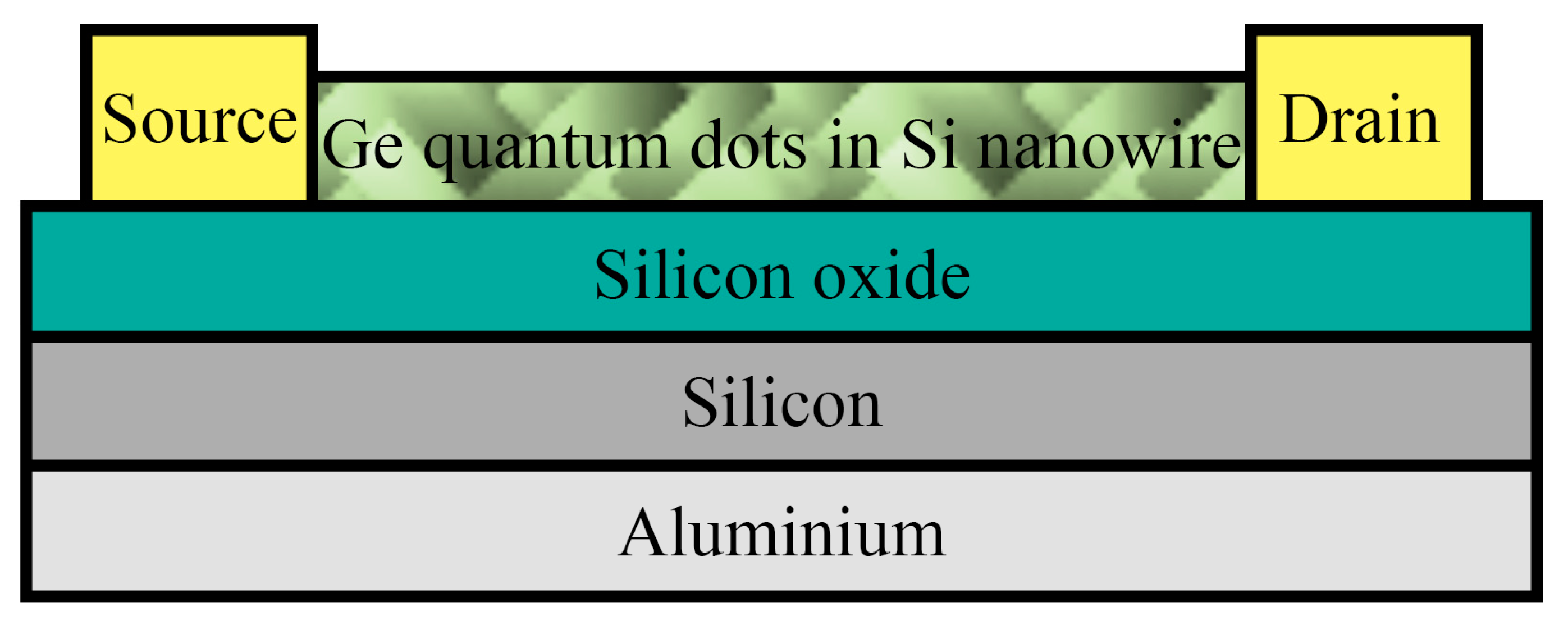
- John, J.W.; Dhyani, V.; Singh, S.; Jakhar, A.; Sarkar, A.; Das, S.; Ray, S.K. Low-noise, high-detectivity, polarization sensitive, room-temperature infrared photodetectors based on Ge quantum dot decorated Si-on-insulator nanowire field effect transistors. Nanotechnology 2021, 32, 315205. [Google Scholar] [CrossRef]
- Zhou, H.; Xu, S.; Wu, S.; Huang, Y.-C.; Zhao, P.; Tong, J.; Son, B.; Guo, X.; Zhang, D.; Gong, X.; et al. Photo detection and modulation from 1,550 to 2,000 nm realized by a GeSn/Ge multiple-quantum-well photodiode on a 300-mm Si substrate. Opt. Express 2020, 28, 34772–34786. [Google Scholar] [CrossRef]
- Li, X.; Peng, L.; Liu, Z.; Zhou, Z.; Zheng, J.; Xue, C.; Zuo, Y.; Chen, B.; Cheng, B. 30 GHz GeSn photodetector on SOI substrate for 2 μm wavelength application. Photonics Res. 2021, 9, 494–500. [Google Scholar] [CrossRef]
- Kumar, H.; Pandey, A.K. GeSn-Based Multiple-Quantum-Well Photodetectors for Mid-Infrared Sensing Applications. IEEE Trans. Nanobiosci. 2022, 21, 175–183. [Google Scholar] [CrossRef]
- Son, B.; Lin, Y.; Lee, K.H.; Margetis, J.; Kohen, D.; Tolle, J.; Tan, C.S. Metal-Semiconductor-Metal Photodetectors on a GeSn-on-Insulator Platform for 2 μm Applications. IEEE Photonics J. 2022, 14, 6824406. [Google Scholar] [CrossRef]
- Timofeev, V.A.; Nikiforov, A.I.; Tuktamyshev, A.R.; Mashanov, V.I.; Loshkarev, I.D.; Bloshkin, A.A.; Gutakovskii, A.K. Pseudomorphic GeSiSn, SiSn and Ge layers in strained heterostructures. Nanotechnology 2018, 29, 154002. [Google Scholar] [CrossRef] [PubMed]
- Timofeev, V.; Nikiforov, A.; Yakimov, A.; Mashanov, V.; Loshkarev, I.; Bloshkin, A.; Kirienko, V.; Novikov, V.; Kareva, K. Studying the morphology, structure and band diagram of thin GeSiSn films and their mid-infrared photoresponse. Semicond. Sci. Technol. 2019, 34, 014001. [Google Scholar] [CrossRef]
- Sun, G.; Soref, R.A.; Khurgin, J.B.; Yu, S.-Q.; Chang, G.-E. Longwave IR lattice matched L-valley Ge/GeSiSn waveguide quantum cascade detector. Opt. Express 2022, 30, 42385–42393. [Google Scholar] [CrossRef]
- Timofeev, A.A.; Mashanov, V.I.; Nikiforov, A.I.; Loshkarev, A.D.; Gulyaev, D.V.; Volodin, V.A.; Kozhukhov, A.S.; Komkov, O.S.; Firsov, D.D.; Korolkov, I.V. Study of structural and optical properties of a dual-band material based on tin oxides and GeSiSn compounds. Appl. Surf. Sci. 2022, 573, 151615. [Google Scholar] [CrossRef]
- Timofeev, V.A.; Mashanov, V.I.; Nikiforov, A.I.; Skvortsov, I.V.; Gayduk, A.E.; Bloshkin, A.A.; Loshkarev, I.D.; Kirienko, V.V.; Kolyada, D.V.; Firsov, D.D.; et al. Tuning the structural and optical properties of GeSiSn/Si multiple quantum wells and GeSn nanostructures using annealing and a faceted surface as a substrate. Appl. Surf. Sci. 2022, 593, 153421. [Google Scholar] [CrossRef]
- Siontas, S.; Li, D.; Wang, H.; Aravind AV, P.S.; Zaslavsky, A.; Pacifici, D. High-performance germanium quantum dot photodetectors in the visible and near infrared. Mater. Sci. Semicond. Process. 2019, 92, 19–27. [Google Scholar] [CrossRef]
- Xu, G.; Cong, H.; Wan, F.; Wang, X.; Xie, C.; Xu, C.; Xue, C. Si-Based Ge 320 × 256 Focal Plane Array for Short-Wave Infrared Imaging. IEEE Photonics Technol. Lett. 2022, 34, 517–520. [Google Scholar] [CrossRef]
- Gao, Y.; Cansizoglu, H.; Polat, K.G.; Ghandiparsi, S.; Kaya, A.; Mamtaz, H.H.; Mayet, A.S.; Wang, Y.; Zhang, X.; Yamada, T. Photon-trapping microstructures enable high-speed high-efficiency silicon photodiodes. Nat. Photonics 2017, 11, 301–308. [Google Scholar] [CrossRef]
- Cansizoglu, H.; Bartolo-Perez, C.; Gao, Y.; Devine, E.P.; Ghandiparsi, S.; Polat, K.G.; Mamtaz, H.H.; Yamada, T.; Elrefaie, A.F.; Wang, S.-Y. Surface-illuminated photon-trapping high-speed Ge-on-Si photodiodes with improved efficiency up to 1700 nm. Photonics Res. 2018, 6, 734–742. [Google Scholar] [CrossRef]
- Kumar, H.; Pandey, A.K.; Lin, C.-H. Optimal design and noise analysis of high-performance DBR-integrated lateral germanium (Ge) photodetectors for SWIR applications. J. Electron Devices Soc. 2022, 10, 649–659. [Google Scholar] [CrossRef]
- Wu, S.; Xu, S.; Zhou, H.; Jin, Y.; Chen, Q.; Huang, Y.-C.; Zhang, L.; Gong, X.; Tan, C.S. High-Performance Back-Illuminated Ge0.92Sn0.08/Ge Multiple-Quantum-Well Photodetector on Si Platform for SWIR Detection. IEEE J. Sel. Top. Quantum Electron. 2022, 28, 8200109. [Google Scholar] [CrossRef]
- Seo, D.; Kwon, W.-B.; Kim, S.C.; Park, C.-S. Frequency Response Estimation of 1.3 μm Waveguide Integrated Vertical PIN Type Ge-on-Si Photodetector Based on the Analysis of Fringing Field in Intrinsic Region. Curr. Opt. Photonics 2019, 3, 510–515. [Google Scholar]
- Hu, X.; Wu, D.; Chen, D.; Wang, L.; Xiao, X.; Yu, S. 180 Gbit/s Si3N4-waveguide coupled germanium photodetector with improved quantum efficiency. Opt. Lett. 2021, 46, 6019–6022. [Google Scholar] [CrossRef]
- Wang, H.; Zhang, J.; Zhang, G.; Chen, Y.; Huang, Y.-C.; Gong, X. High-speed and high-responsivity p-i-n waveguide photodetector at a 2 μm wavelength with a Ge0.92Sn0.08/Ge multiple-quantum-well active layer. Opt. Lett. 2021, 46, 2099–2102. [Google Scholar] [CrossRef] [PubMed]
- Cui, J.; Chen, H.; Zhou, J.; Li, T. High Performance Ge-on-Si Photodetector With Optimized Light Field Distribution by Dual-Injection. IEEE Photonics J. 2022, 14, 6817304. [Google Scholar] [CrossRef]
- Fu, Z.; Yu, H.; Wei, Z.; Xia, P.; Zhang, Q.; Wang, X.; Huang, Q.; Wang, Y.; Yang, J. High-Power and High-Speed Ge/Si Traveling-Wave Photodetector Optimized by Genetic Algorithm. J. Light. Technol. 2022, 41, 240–248. [Google Scholar] [CrossRef]
- Wang, H.; Chen, Y.; Zhang, G.; Zhang, J.; Xu, H.; Huang, Y.-C.; Gong, X. Monolithic Waveguide-Integrated Group IV Multiple-Quantum-Well Photodetectors on 300 mm Si Substrates. IEEE Trans. Electron Devices 2022, 69, 2166–2172. [Google Scholar] [CrossRef]
- Wang, H.; Zhang, J.; Zhang, G.; Chen, Y.; Han, K.; Huang, Y.-C.; Gong, X. Monolithic Waveguide Group IV Multiple-Quantum-Well Photodetectors and Modulators on 300-mm Si Substrates for 2-μm Wavelength Optoelectronic Integrated Circuit. IEEE Trans. Electron Devices 2022, 69, 7161–7166. [Google Scholar] [CrossRef]
- Wei, Z.; Yu, H.; Fu, Z.; Xia, P.; Zhang, Q.; Ning, N.; Huang, Q.; Wang, Y.; Yang, J. Silicon-based high-power traveling wave photodetector with inductive gain peaking. Opt. Express 2022, 30, 46094–46105. [Google Scholar] [CrossRef]
- Sia JX, B.; Li, X.; Wang, J.; Wang, W.; Qiao, Z.; Guo, X.; Lee, C.W.; Sasidharan, A.; Gunasagar, S.; Littlejohns, C.G.; et al. Wafer-Scale Demonstration of Low-Loss (~0.43 dB/cm), High-Bandwidth (>38 GHz), Silicon Photonics Platform Operating at the C-Band. IEEE Photonics J. 2022, 14, 6628609. [Google Scholar]
- Li, Y.; Liu, X.; Li, X.; Wang, S.; Ye, H.; Zhang, L.; Li, Y.; Sun, S.; Chen, B.; Ma, Y.; et al. Surface illuminated interdigitated Ge-on-Si photodetector with high responsivity. Opt. Express 2021, 29, 16346–16361. [Google Scholar] [CrossRef] [PubMed]
- Kumari, K.; Kumar, S.; Mehta, M.; Chatterjee, A.; Selvaraja, S.K.; Avasthi, S. Laser-Crystallized Epitaxial Germanium on Silicon-Based Near-Infrared Photodetector. IEEE Sens. J. 2022, 22, 11682–11689. [Google Scholar] [CrossRef]
- Izhnin, I.I.; Kurbanov, K.R.; Lozovoy, K.A.; Kokhanenko, A.P.; Dirko, V.V.; Voitsekhovskii, A.V. Epitaxial fabrication of 2D materials of group IV elements. Appl. Nanosci. 2020, 10, 4375–4383. [Google Scholar] [CrossRef]
- Dushaq, G.; Paredes, B.; Villegas, J.E.; Tamalampudi, S.R.; Rasras, M. On-chip integration of 2D Van der Waals germanium phosphide (GeP) for active silicon photonics devices. Opt. Express 2022, 30, 15986–15997. [Google Scholar] [CrossRef] [PubMed]
- Lozovoy, K.A.; Dirko, V.V.; Vinarskiy, V.P.; Kokhanenko, A.P.; Voitsekhovskii, A.V.; Akimenko, N.Y. Two-dimensional materials of group IVA: Latest advances in epitaxial methods of growth. Russ. Phys. J. 2022, 64, 1583–1591. [Google Scholar] [CrossRef]
- Guskov, A.; Lavrov, S.; Galiev, R. Polarization sensitive photodetectors based on two-dimensional WSe2. Nanomaterials 2022, 12, 1854. [Google Scholar] [CrossRef]
- Lozovoy, K.A.; Izhnin, I.I.; Kokhanenko, A.P.; Dirko, V.V.; Vinarskiy, V.P.; Voitsekhovskii, A.V.; Fitsych, O.I.; Akimenko, N.Y. Single-element 2D materials beyond graphene: Methods of epitaxial synthesis. Nanomaterials 2022, 12, 2221. [Google Scholar] [CrossRef]
- Novikov, A.; Smagina, Z.; Stepikhova, M.; Zinovyev, V.; Rudin, S.; Dyakov, S.; Rodyakina, E.; Nenashav, A.; Sergeev, S.; Peretokin, A.; et al. One-stage formation of two-dimensional photonic crystal and spatially ordered arrays of self-assembled Ge(Si) nanoislands on pit-patterned silicon-on-insulator substrate. Nanomaterials 2021, 11, 909. [Google Scholar] [CrossRef]
- Tsai, C.H.; Huang, B.J.; Soref, R.A.; Sun, G.; Cheng, H.H.; Chang, G. GeSn resonant-cavity-enhanced photodetectors for efficient photodetection at the 2 μm wavelength band. Opt. Lett. 2020, 45, 1463–1466. [Google Scholar] [CrossRef]
- Berkmann, F.; Augel, L.; Hack, M.; Kawaguchi, Y.; Weisshaupt, D.; Fischer, I.A.; Schulze, J. Optimization of Fully Integrated Al Nanohole Array-Based Refractive Index Sensors for Use With a LED Light Source. IEEE Photonics J. 2022, 14, 4831708. [Google Scholar] [CrossRef]
- Srikam, S.; Traiwattanapong, W.; Limsuwan, P.; Chaisakul, P. An FDTD Investigation of Compact and Low-Voltage Waveguide-Integrated Plasmonic Ge/SiGe Multiple Quantum Wells Photodetectors. IEEE Photonics J. 2022, 14, 6650207. [Google Scholar] [CrossRef]
- Zhou, H.; Zhang, L.; Tong, J.; Wu, S.; Son, B.; Chen, Q.; Zhang, D.H.; Tan, C.S. Surface plasmon enhanced GeSn photodetectors operating at 2 μm. Opt. Express 2021, 29, 8498–8509. [Google Scholar] [CrossRef] [PubMed]
- Huang, J.; Guo, D.; Deng, Z.; Chen, W.; Liu, H.; Wu, J.; Chen, B. Midwave Infrared Quantum Dot Quantum Cascade Photodetector Monolithically Grown on Silicon Substrate. J. Light. Technol. 2018, 36, 4033–4038. [Google Scholar] [CrossRef]
- Masala, S.; Adinolfi, V.; Sun, J.-P.; Del Gobbo, S.; Voznyy, O.; Kramer, I.J.; Hill, I.G.; Sargent, E.H. The silicon:colloidal quantum dot heterojunction. Adv. Mater. 2015, 27, 7445–7450. [Google Scholar] [CrossRef]
- Xu, K.; Xiao, X.; Zhou, W.; Jiang, X.; Wei, Q.; Chen, H.; Deng, Z.; Huang, J.; Chen, B.; Ning, Z. Inverted Si:PbS colloidal quantum dot heterojunction-based infrared photodetector. ACS Appl. Mater. Interfaces 2020, 12, 15414–15421. [Google Scholar] [CrossRef]
- Xiao, X.; Xu, K.; Yin, M.; Qiu, Y.; Zheng, L.; Cheng, X.; Yu, Y.; Ning, Z. High quality silicon: Colloidal quantum dot heterojunction based infrared photodetector. Appl. Phys. Lett. 2020, 116, 101102. [Google Scholar] [CrossRef]
- Xu, Q.; Hu, J.; Wang, X. On-chip Ge, InGaAs, and colloidal quantum dot photodetectors: Comparisons for application in silicon photonics. J. Opt. Soc. Am. B 2021, 38, 194–200. [Google Scholar] [CrossRef]
- Lin, Y.; Lee, K.H.; Son, B.; Tan, C.S. Low-power and high-detectivity Ge photodiodes by in-situ heavy As doping during Ge-on-Si seed layer growth. Opt. Express 2021, 29, 2940–2952. [Google Scholar] [CrossRef]
- Zhu, J.; Zhu, H.; Liu, M.; Wang, Y.; Xu, H.; Ali, N.; Deng, H.; Tan, Z.; Cao, J.; Dai, N.; et al. Ultrabroadband and multiband infrared/terahertz photodetectors with high sensitivity. Photonics Res. 2021, 9, 2167–2175. [Google Scholar] [CrossRef]
- Son, B.; Zhou, H.; Lin, Y.; Lee, K.H.; Tan, C.S. Gourd-shaped hole array germanium (Ge)-on-insulator photodiodes with improved responsivity and specific detectivity at 1,550 nm. Opt. Express 2021, 29, 16520–16533. [Google Scholar] [CrossRef]
- Li, F.; Han, H.; Chen, Q.; Zhang, B.; Bao, H.; Dai, Y.; Ge, R.; Guo, S.; He, G.; Fei, Y.; et al. Saturation efficiency for detecting 1550 nm photons with a 2 × 2 array of Mo0.8Si0.2 nanowires at 2.2 K. Photonics Res. 2021, 9, 389–394. [Google Scholar] [CrossRef]
- Yuan, Y.; Hyang, Z.; Zeng, X.; Liang, D.; Sorin, W.V.; Fiorentino, M.; Beausoleil, R.G. High Responsivity Si-Ge Waveguide Avalanche Photodiodes Enhanced by Loop Reflector. IEEE J. Sel. Top. Quantum Electron. 2022, 28, 3800508. [Google Scholar] [CrossRef]
- Benedikovic, D.; Virot, L.; Aubin, G.; Hartmann, J.-M.; Amar, F.; Le Roux, X.; Alonso-Ramos, C.; Cassan, E.; Marris-Morini, D.; Boeuf, F.; et al. Silicon-Germanium Avalanche Receivers With fJ/bit Energy Consumption. IEEE J. Sel. Top. Quantum Electron. 2022, 28, 3802508. [Google Scholar] [CrossRef]
- Pang, Y.; Liu, Z.; Liu, X.; Zhang, D.; Niu, C.; Li, M.; Zheng, J.; Zuo, Y.; Cheng, B. High-performance waveguide-coupled lateral Ge/Si avalanche photodetector. Opt. Lett. 2022, 47, 4463–4466. [Google Scholar] [CrossRef]
- Benedikovic, D.; Virot, L.; Aubin, G.; Hartmann, J.-M.; Amar, F.; Le Roux, X.; Alonso-Ramos, C.; Cassan, E.; Marris-Morini, D.; Fedeli, J.-M.; et al. Silicon–germanium receivers for short-wave-infrared optoelectronics and communications. Nanophotonics 2021, 10, 1059–1079. [Google Scholar] [CrossRef]
- Izhnin, I.I.; Lozovoy, K.A.; Kokhanenko, A.P.; Khomyakova, K.I.; Douhan, R.M.H.; Dirko, V.V.; Voitsekhovskii, A.V.; Fitsych, O.I.; Akimenko, N.Y. Single-photon avalanche diode detectors based on group IV materials. Appl. Nanosci. 2022, 12, 253–263. [Google Scholar] [CrossRef]
- Wang, B.; Mu, J. High-speed Si-Ge avalanche photodiodes. PhotoniX 2022, 3, 8. [Google Scholar] [CrossRef]
- Vines, P.; Kuzmenko, K.; Kirdoda, J.; Dumas DC, S.; Mirza, M.M.; Millar, R.W.; Paul, D.J.; Buller, G.S. High performance planar germanium-on-silicon single-photon avalanche diode detectors. Nat. Commun. 2019, 10, 1086. [Google Scholar] [CrossRef] [Green Version]
- Llin, L.F.; Kirdoda, J.; Thorburn, F.; Huddleston, L.L.; Greener, Z.M.; Kuzmenko, K.; Vines, P.; Dumas DC, S.; Millar, R.W.; Buller, G.S.; et al. High sensitivity Ge-on-Si single-photon avalanche diode detectors. Opt. Lett. 2020, 45, 6406–6409. [Google Scholar] [CrossRef]
- Das, R.; Xie, Y.; Frankis, H.; Chen, K.; Rufenacht, H.; Lamontagne, G.; Bradley JD, B.; Knights, A.P. Gain-enabled optical delay readout unit using CMOS-compatible avalanche photodetectors. Photonics Res. 2022, 10, 2422–2433. [Google Scholar] [CrossRef]
- Marris-Morini, D.; Vakarin, V.; Ramirez, J.M.; Liu, Q.; Ballabio, A.; Frigerio, J.; Montesinos, M.; Alonso-Ramos, C.; Le Roux, X.; Serna, S.; et al. Germanium-based integrated photonics from near- to mid-infrared applications. Nanophotonics 2018, 7, 1781–1793. [Google Scholar] [CrossRef]
- Koerner, R.; Fischer, I.A.; Schwarz, D.; Clausen, C.J.; Hoppe, N.; Schulze, J. Engineering of Germanium Tunnel Junctions for Optical Applications. IEEE Photonics J. 2018, 10, 2200912. [Google Scholar] [CrossRef]
- Stepikhova, M.V.; Novikov, A.V.; Yablonskiy, A.N.; Shaleev, M.V.; Utkin, D.E.; Rutckaia, V.V.; Skorokhodov, E.V.; Sergeev, S.M.; Yurasov, D.V.; Krasilnik, Z.F. Light emission from Ge(Si)/SOI self-assembled nanoislands embedded in photonic crystal slabs of various periods with and without cavities. Semicond. Sci. Technol. 2019, 34, 024003. [Google Scholar] [CrossRef]
- Peretokin, A.V.; Stepikhova, M.V.; Novikov, A.V.; Dyakov, S.A.; Zinovieva, A.F.; Smagina, Z.h.V.; Nasimov, D.A.; Rodyakina, E.E.; Zinovyev, V.A. Photonic crystal band structure in luminescence response of samples with Ge/Si quantum dots grown on pit-patterned SOI substrates. Photonics Nanostruct.—Fundam. Appl. 2023, 53, 101093. [Google Scholar] [CrossRef]
- Stange, D.; Wirths, S.; Geiger, R.; Schulte-Braucks, C.; Marzban, B.; Von Den Driesch, N.; Mussler, G.; Zabel, T.; Stoica, T.; Hartmann, J.M.; et al. Optically pumped GeSn microdisk lasers on Si. ACS Photonics 2016, 3, 1279–1285. [Google Scholar] [CrossRef]
- Al-Kabi, S.; Ghetmiri, S.A.; Margetis, J.; Pham, T.; Zhou, Y.; Dou, W.; Collier, B.; Quinde, R.; Du, W.; Mosleh, A.; et al. An optically pumped 2.5 μm GeSn laser on Si operating at 110 K. Appl. Phys. Lett. 2016, 109, 171105. [Google Scholar] [CrossRef]
- Reboud, V.; Gassenq, A.; Pauc, N.; Aubin, J.; Milord, L.; Thai, Q.M.; Bertrand, M.; Guilloy, K.; Rouchon, D.; Rothman, J.; et al. Optically pumped GeSn micro-disks with 16% Sn lasing at 3.1 μm up to 180 K. Appl. Phys. Lett. 2017, 111, 092101. [Google Scholar] [CrossRef] [Green Version]
- Savvin, A.; Dormidonov, A.; Smetanina, E.; Mitrokhin, V.; Lipatov, E.; Genin, D.; Potanin, S.; Yelisseyev, A.; Vins, V. NV—Diamond laser. Nat. Commun. 2021, 12, 7118. [Google Scholar] [CrossRef]
- Wang, L.; Zhang, Y.; Sun, H.; You, J.; Miao, Y.; Dong, Z.; Liu, T.; Jiang, Z.; Hu, H. Nanoscale growth of a Sn-guided SiGeSn alloy on Si (111) substrates by molecular beam epitaxy. Nanoscale Adv. 2021, 3, 997. [Google Scholar] [CrossRef]
- Lozovoy, K.A.; Kokhanenko, A.P.; Dirko, V.V.; Akimenko, N.Y.; Voitsekhovskii, A.V. Evolution of epitaxial quantum dots formed by Volmer–Weber growth mechanism. Cryst. Growth Des. 2019, 19, 7015–7021. [Google Scholar] [CrossRef]
- Wang, S.; Zhang, N.; Chen, P.; Wang, L.; Yang, X.; Jiang, Z.; Zhong, Z. Toward precise site-controlling of self-assembled Ge quantum dots on Si microdisks. Nanotechnology 2018, 29, 345606. [Google Scholar] [CrossRef] [PubMed]
- Dirko, V.V.; Lozovoy, K.A.; Kokhanenko, A.P.; Voitsekhovskii, A.V. Thickness-dependent elastic strain in Stranski–Krastanow growth. Phys. Chem. Chem. Phys. 2020, 22, 19318–19325. [Google Scholar] [CrossRef] [PubMed]
- Liu, K.; Berbezier, I.; Favre, L.; Ronda, A.; Abbarchi, M.; Donnadieu, P.; Voorhees, P.W.; Aqua, J.-N. Capillary-driven elastic attraction between quantum dots. Nanoscale 2019, 11, 7798–7804. [Google Scholar] [CrossRef] [PubMed] [Green Version]
- Lozovoy, K.A.; Zhou, Y.; Smith, R.; Lloyd, A.; Kokhanenko, A.P.; Dirko, V.V.; Akimenko, N.Y.; Grigoryev, D.V.; Voitsekhovskii, A.V. Thickness-dependent surface energy and formation of epitaxial quantum dots. Thin Solid Film. 2020, 713, 138363. [Google Scholar] [CrossRef]
- Shklyaev, A.A.; Tsarev, A.V. Broadband Antireflection Coatings Made of Resonant Submicron- and Micron-Sized SiGe Particles Grown on Si Substrates. IEEE Photonics J. 2021, 13, 2200212. [Google Scholar] [CrossRef]
- Nikiforov, A.; Timofeev, V.; Mashanov, V.; Azarov, I.; Loshkarev, I.; Volodin, V.; Gulyaev, D.; Chetyrin, I.; Korolkov, I. Formation of SnO and SnO2 phases during the annealing of SnO(x) films obtained by molecular beam epitaxy. Appl. Surf. Sci. 2020, 512, 145735. [Google Scholar] [CrossRef]
- Dirko, V.V.; Lozovoy, K.A.; Kokhanenko, A.P.; Voitsekhovskii, A.V. High-resolution RHEED analysis of dynamics of low-temperature superstructure transitions in Ge/Si(001) epitaxial system. Nanotechnology 2022, 33, 115603. [Google Scholar] [CrossRef]
- Timofeev, V.; Mashanov, V.; Nikiforov, A.; Gutakovskii, A.; Gavrilova, T.; Skvortsov, I.; Gulyaev, D.; Firsov, D.; Komkov, O. Epitaxial growth of peculiar GeSn and SiSn nanostructures using a Sn island array as a seed. Appl. Surf. Sci. 2021, 553, 149572. [Google Scholar] [CrossRef]
- Dirko, V.V.; Lozovoy, K.A.; Kokhanenko, A.P.; Kukenov, O.I.; Korotaev, A.G.; Voitsekhovskii, A.V. Peculiarities of the 7 × 7 to 5 × 5 superstructure transition during epitaxial growth of germanium on silicon (111) surface. Nanomaterials 2023, 13, 231. [Google Scholar] [CrossRef]
- Rutckaia, V.; Heyroth, F.; Novikov, A.; Shaleev, M.; Petrov, M.; Schilling, J. Quantum dot emission driven by Mie resonances in silicon nanostructures. Nano Lett. 2017, 17, 6886–6892. [Google Scholar] [CrossRef]
- Bai, X.; Purcell-Milton, F.; Gun’ko, Y.K. Optical Properties, Synthesis, and Potential Applications of Cu-Based Ternary or Quaternary Anisotropic Quantum Dots, Polytypic Nanocrystals, and Core/Shell Heterostructures. Nanomaterials 2019, 9, 85. [Google Scholar] [CrossRef] [PubMed] [Green Version]
- de Mello Donegá, C. Synthesis and properties of colloidal heteronanocrystals. Chem. Soc. Rev. 2011, 40, 1512–1546. [Google Scholar] [CrossRef] [PubMed]
- Zora, A.; Triberis, G.P.; Simserides, C. Near-Field Optical Properties of Quantum Dots, Applications and Perspectives. Recent Pat. Nanotechnol. 2011, 5, 188. [Google Scholar] [CrossRef] [PubMed]
- Bera, D.; Qian, L.; Tseng, T.-K.; Holloway, P.H. Quantum Dots and Their Multimodal Applications: A Review. Materials 2010, 3, 2260–2345. [Google Scholar] [CrossRef] [Green Version]
- Vukusic, L.; Kukucka, J.; Watzinger, H.; Milem, J.M.; Schaffler, F.; Katsaros, G. Single-shot readout of hole spins in Ge. Nano Lett. 2018, 18, 7141–7145. [Google Scholar] [CrossRef] [Green Version]
- Watzinger, H.; Kukucka, J.; Vukusic, L.; Gao, F.; Wang, T.; Schaffler, F.; Zhang, J.-J.; Katsaros, G. A germanium hole spin qubit. Nat. Commun. 2018, 9, 3902. [Google Scholar] [CrossRef] [Green Version]
- Hendrickx, N.W.; Lawrie WI, L.; Russ, M.; von Riggelen, F.; de Snoo, S.L.; Schouten, R.N.; Sammak, A.; Scappucci, G.; Veldhorst, M. A four-qubit germanium quantum processor. Nature 2021, 591, 580–585. [Google Scholar] [CrossRef]
- Takeda, K.; Noiri, A.; Nakajima, T.; Kobayashi, T.; Tarucha, S. Quantum error correction with silicon spin qubits. Nature 2022, 608, 682–686. [Google Scholar] [CrossRef]
- Warren, A.; Economou, S.E. Silicon qubits get closer to achieving error correction. Nature 2022, 601, 320–322. [Google Scholar] [CrossRef]


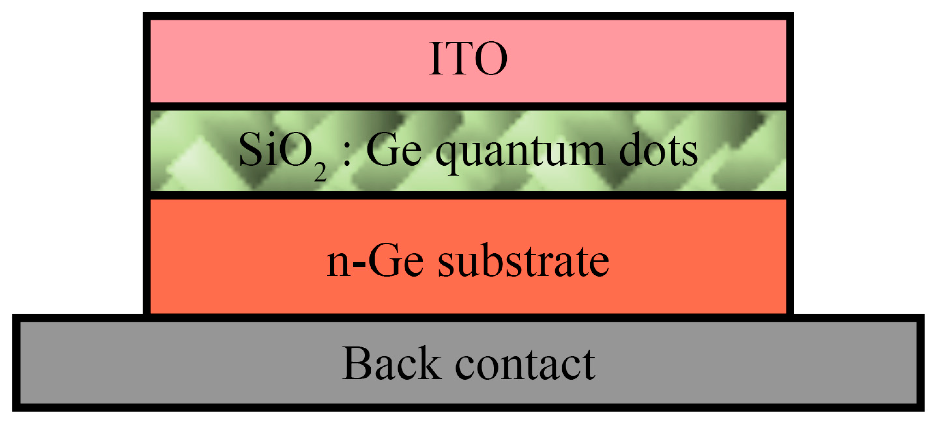
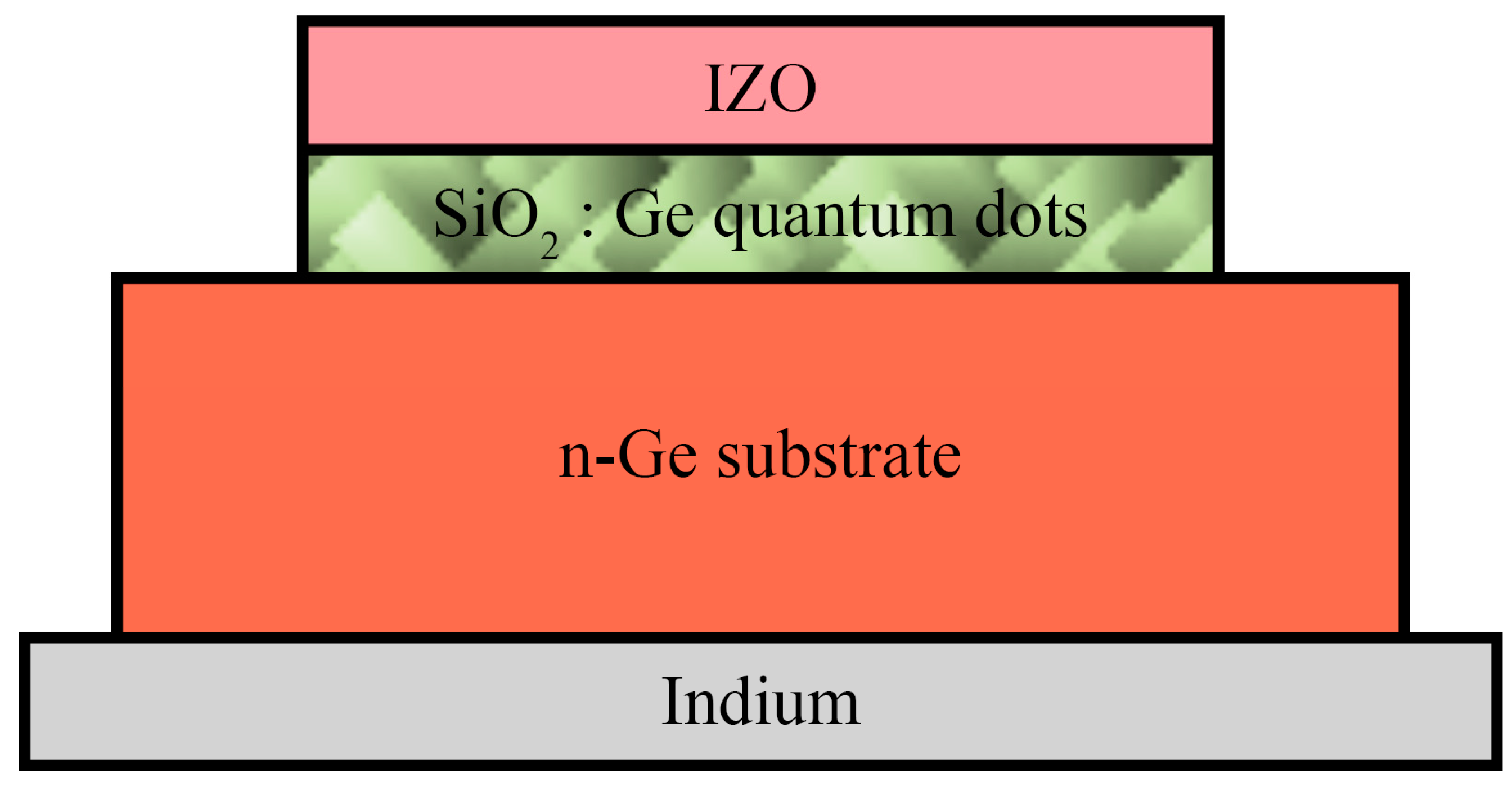
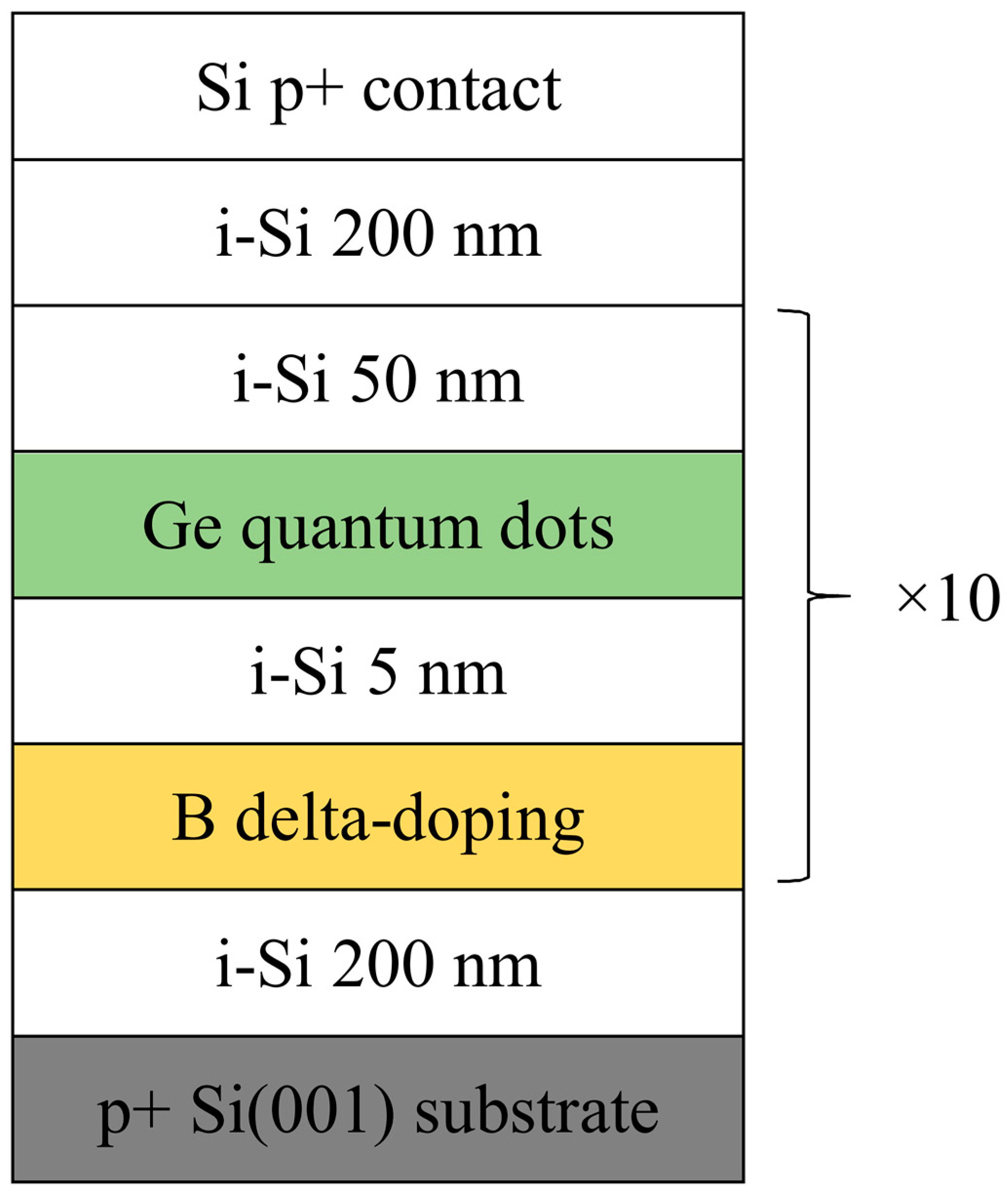
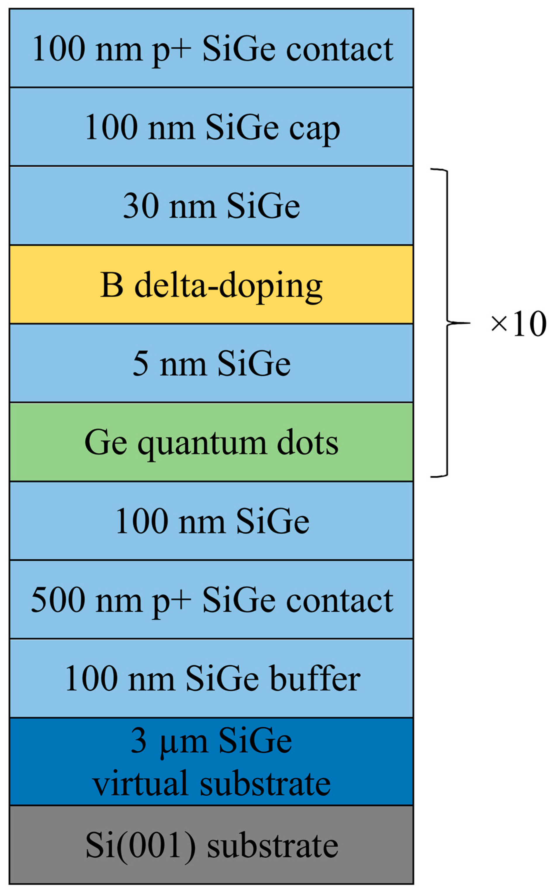
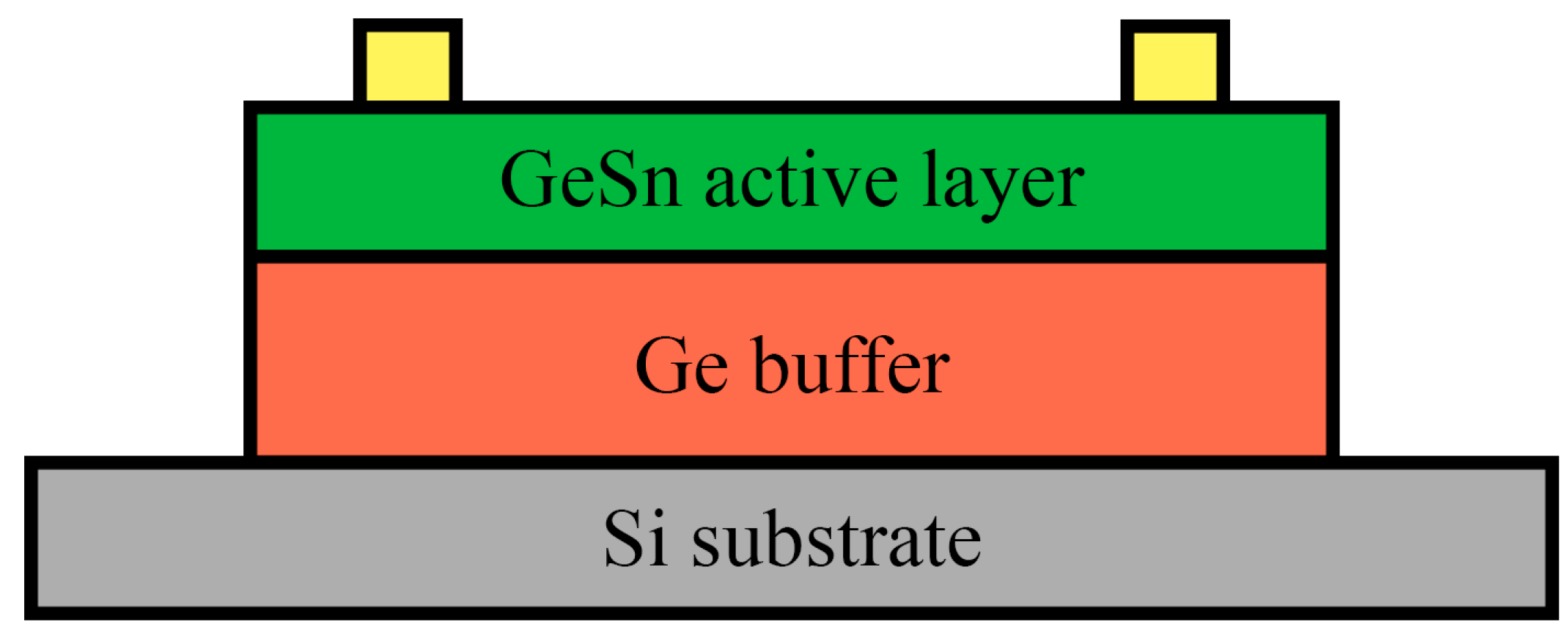
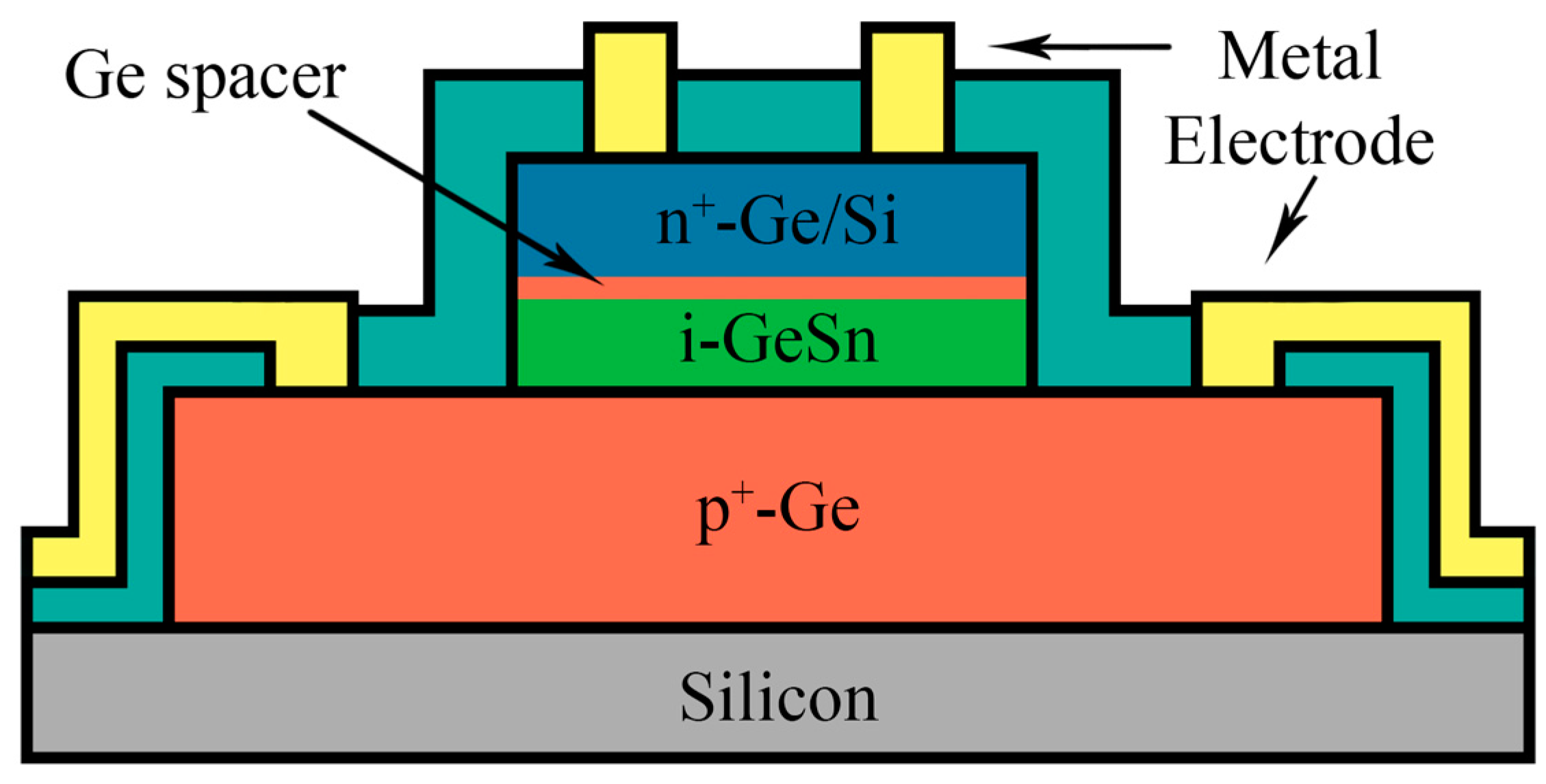
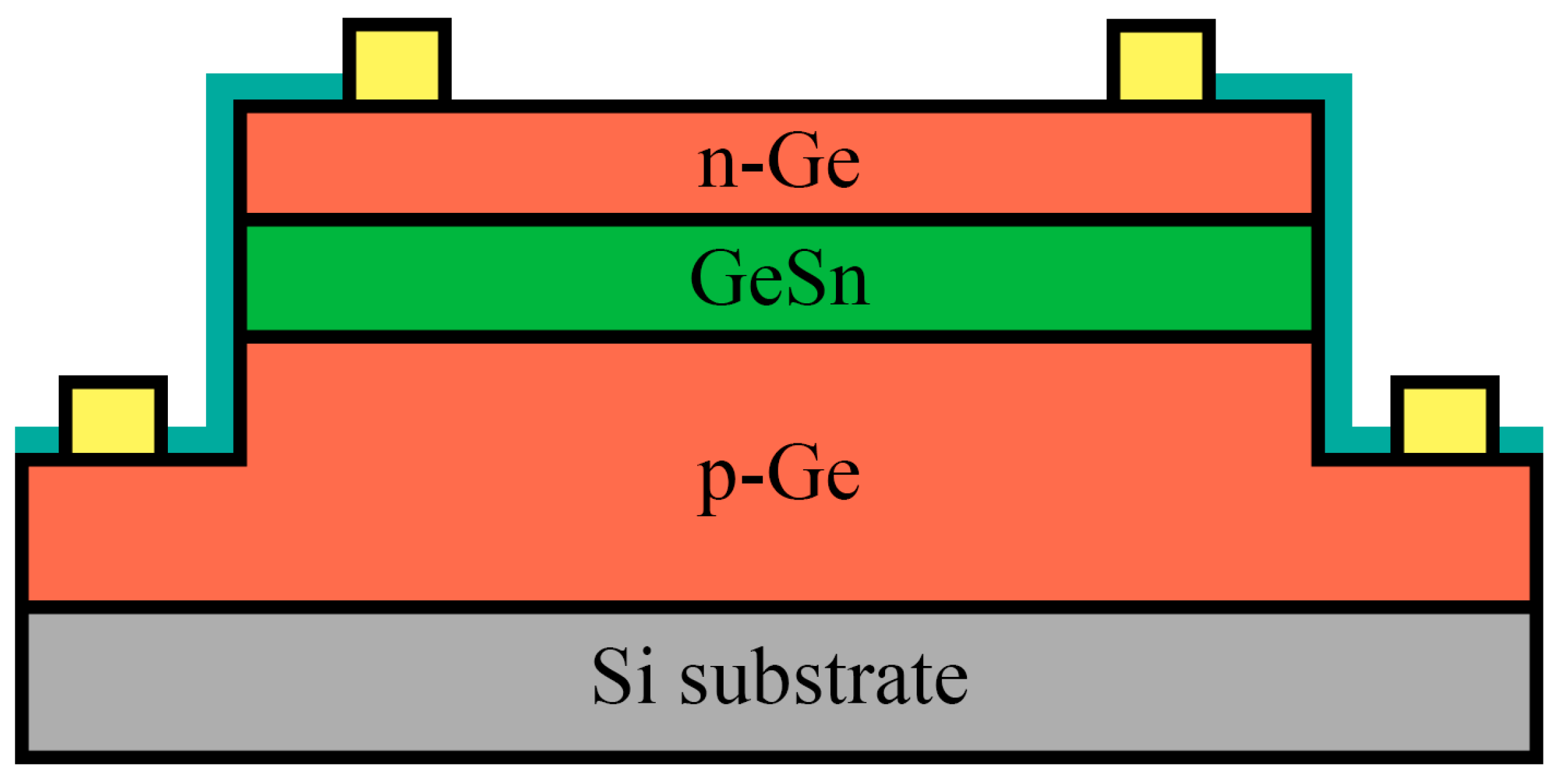
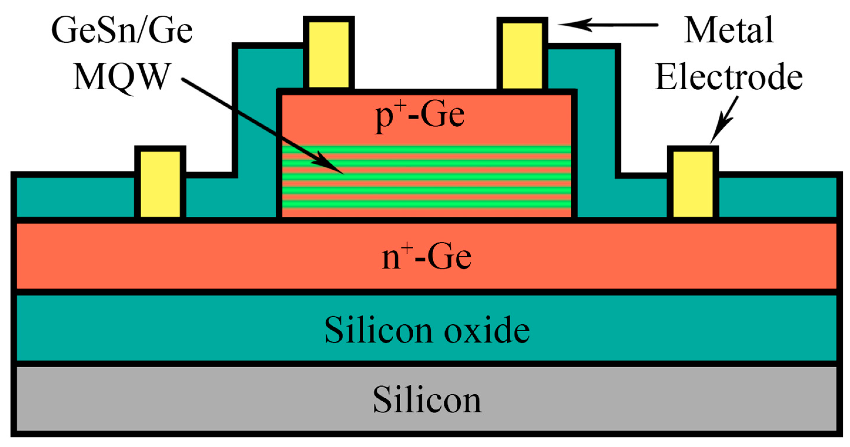
| Model | Wavelength | Responsivity | Dark Current Density | Detectivity |
|---|---|---|---|---|
| nm | A/W | mA/cm2 | cm·Hz1/2·W−1 | |
| One layer GeSn/Ge photoconductor [24] | 1550– 2000 | 0.18 | – | 1.0·109 |
| One layer Ge/GeSn/Ge p-i-n photodiode [25] | 1550 | 0.22 | 70 | – |
| One layer Ge/GeSn/Ge photodetector [26] | 1550– 2600 | 0.30 | 10 | 4.0·109 |
| Black silicon Ge-on-Si p-i-n photodiode [27] | 1550 | 0.34 | 150 | – |
| Multiple quantum wells GeSn/Ge photodetector [28] | 1550– 2200 | 0.11 | 40 | 2.1·108 |
| Multiple quantum wells GeSn/Ge photodetector [48] | 1550– 2200 | 0.31 | 16 | 1.4·1010 |
| One layer SiO2: Ge QDs/Ge photodetector [41] | 640– 1550 | 0.47 | – | – |
| One layer SiO2: Ge QDs/Ge photodetector [42] | 400– 1550 | 1.12 | – | 2.0·1010 |
| Multiple layer Ge QDs/Si photodetector [43] | up to 4000 | 0.43 | 10−6 | 6.2·1010 |
| Multiple layer Ge QDs/SiGe photodetector [44] | up to 6000 | 40 | – | 1.4·1011 |
| Si nanowire: Ge QDs/SiO2/Si phototransistor [47] | 1200– 1700 | 5.50 | – | 9.3·1011 |
Disclaimer/Publisher’s Note: The statements, opinions and data contained in all publications are solely those of the individual author(s) and contributor(s) and not of MDPI and/or the editor(s). MDPI and/or the editor(s) disclaim responsibility for any injury to people or property resulting from any ideas, methods, instructions or products referred to in the content. |
© 2023 by the authors. Licensee MDPI, Basel, Switzerland. This article is an open access article distributed under the terms and conditions of the Creative Commons Attribution (CC BY) license (https://creativecommons.org/licenses/by/4.0/).
Share and Cite
Douhan, R.; Lozovoy, K.; Kokhanenko, A.; Deeb, H.; Dirko, V.; Khomyakova, K. Recent Advances in Si-Compatible Nanostructured Photodetectors. Technologies 2023, 11, 17. https://doi.org/10.3390/technologies11010017
Douhan R, Lozovoy K, Kokhanenko A, Deeb H, Dirko V, Khomyakova K. Recent Advances in Si-Compatible Nanostructured Photodetectors. Technologies. 2023; 11(1):17. https://doi.org/10.3390/technologies11010017
Chicago/Turabian StyleDouhan, Rahaf, Kirill Lozovoy, Andrey Kokhanenko, Hazem Deeb, Vladimir Dirko, and Kristina Khomyakova. 2023. "Recent Advances in Si-Compatible Nanostructured Photodetectors" Technologies 11, no. 1: 17. https://doi.org/10.3390/technologies11010017