
Design of a Half-Bridge Current-Source Inverter Topology for Avionic Systems


Abstract
:1. Introduction
1.1. Theoretical Background
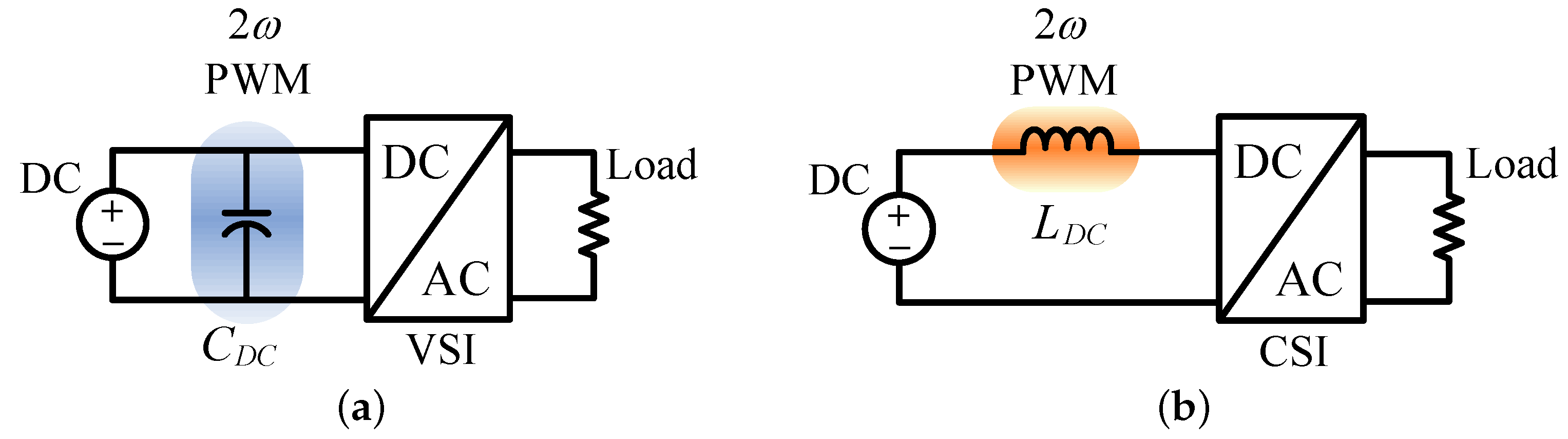
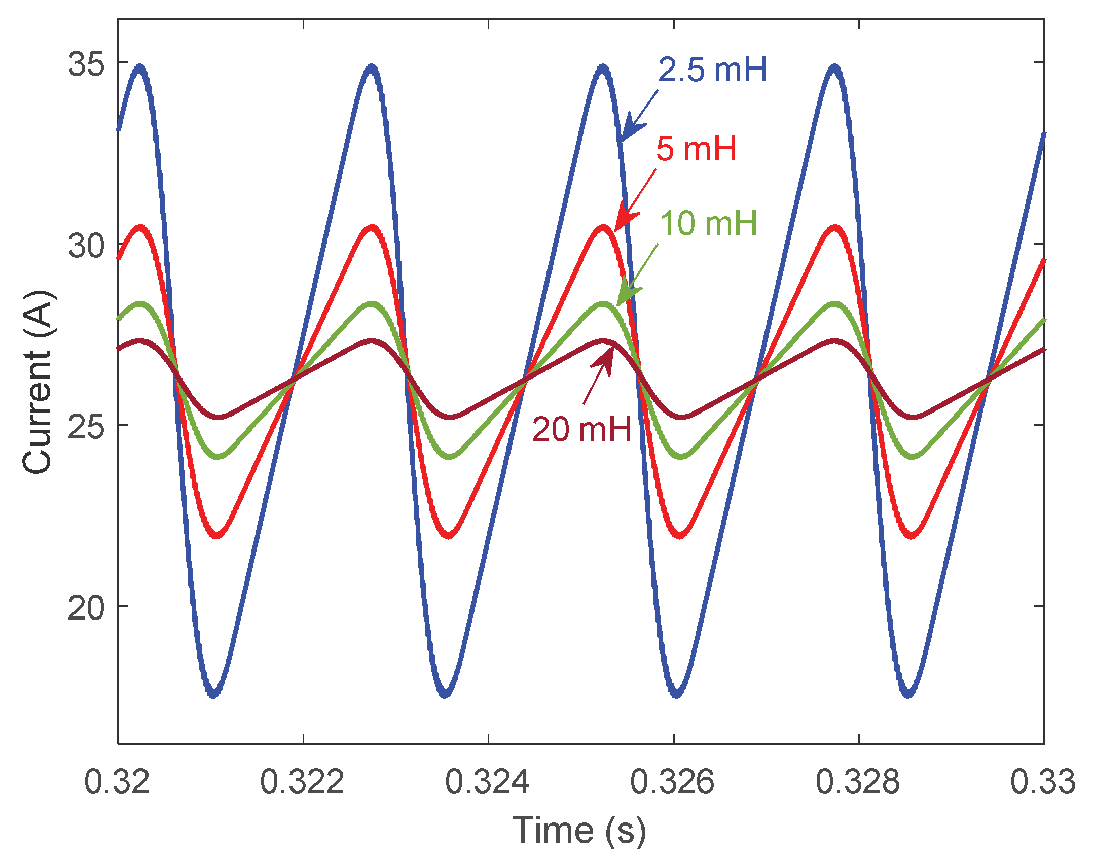
1.2. Current-Source Inverter
- The maximum acceptable input current or voltage ripple causing average power loss at the output of the DC supply.
- The maximum acceptable current ripple (for CSI) or voltage ripple (for VSI) at the input of the inverter causing distortion before an unacceptable level found in the output current of the inverter feeding a load.
- They do not need a large capacitor at the DC link as it affects the lifetime and reliability of the inverter;
- No freewheeling diodes are required when operating into an inductive load, therefore the cost of the system is reduced;
- They can survive an output short circuit thereby allowing fault ride-through properties.
- CSIs can handle capacitive loads relatively easily, however, capacitive loads can cause large current spikes in a VSI;
- Power switches are highly utilized, unlike the VSIs, the current from the supply is switching between them, therefore the switches conduct for a full conducting cycle;
- CSIs have a higher output voltage than the input voltage. VSI topology is acting as a buck converter and it features an output voltage lower than the input voltage;
- The EMI generation is low compared to VSIs as changing currents generates EMI; however, CSIs have substantially constant current.
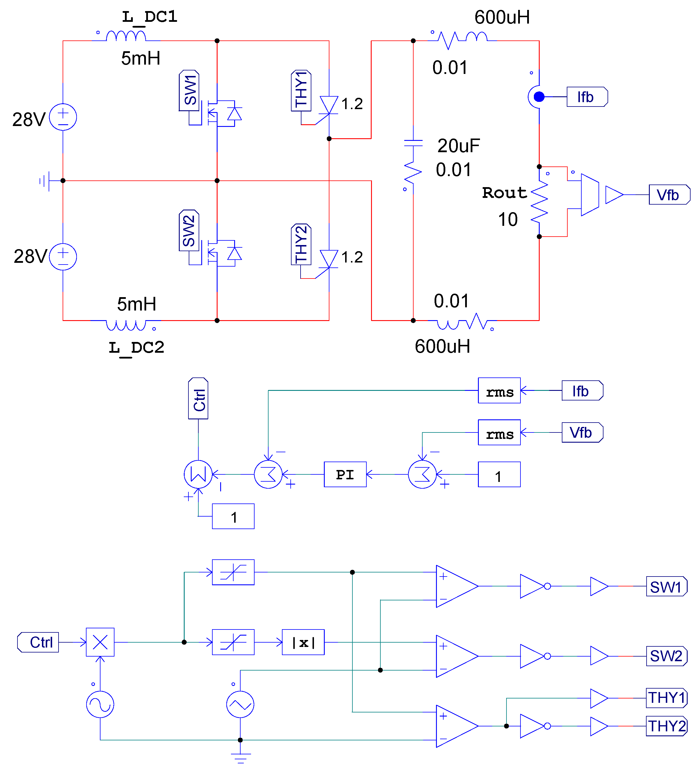
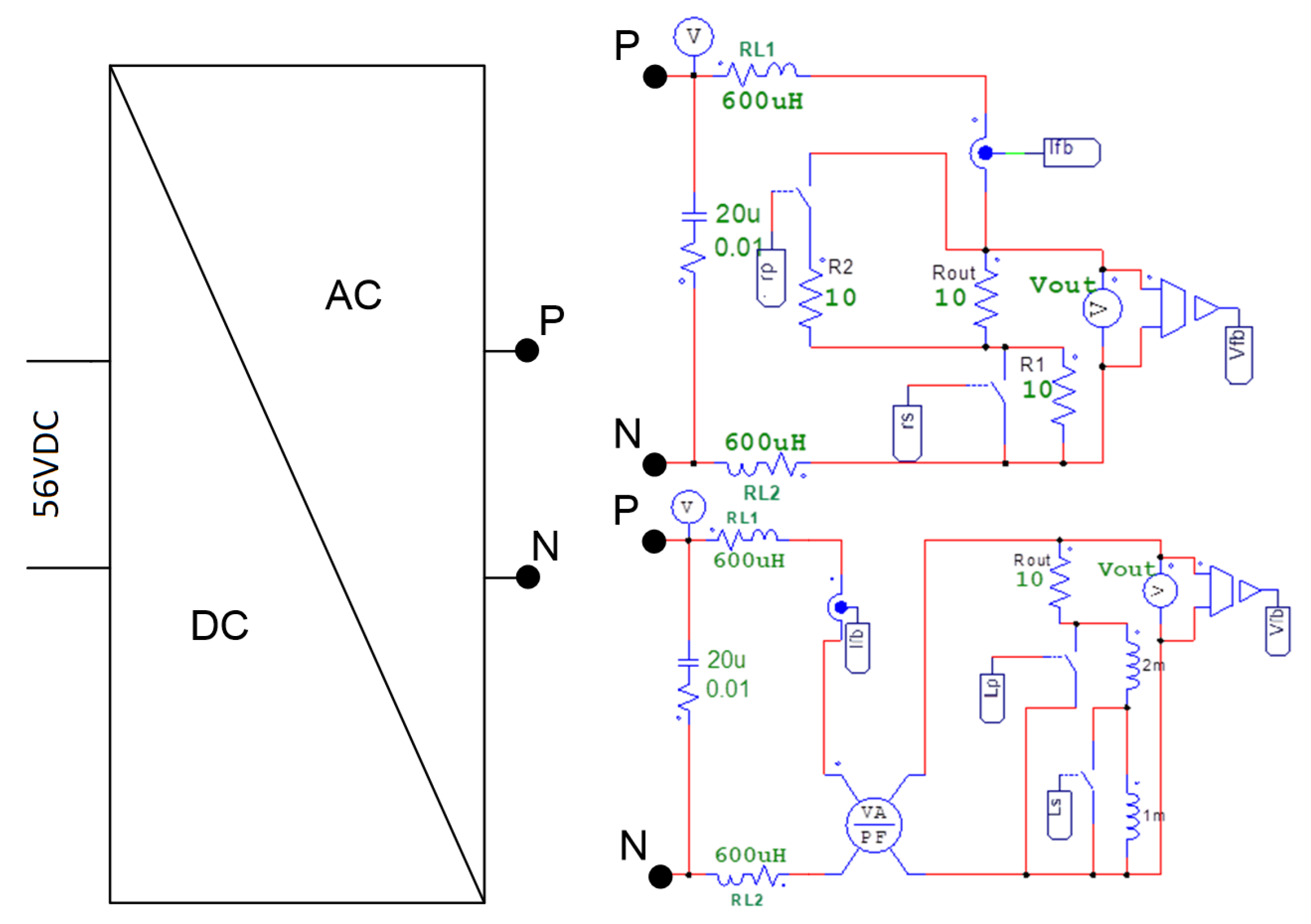
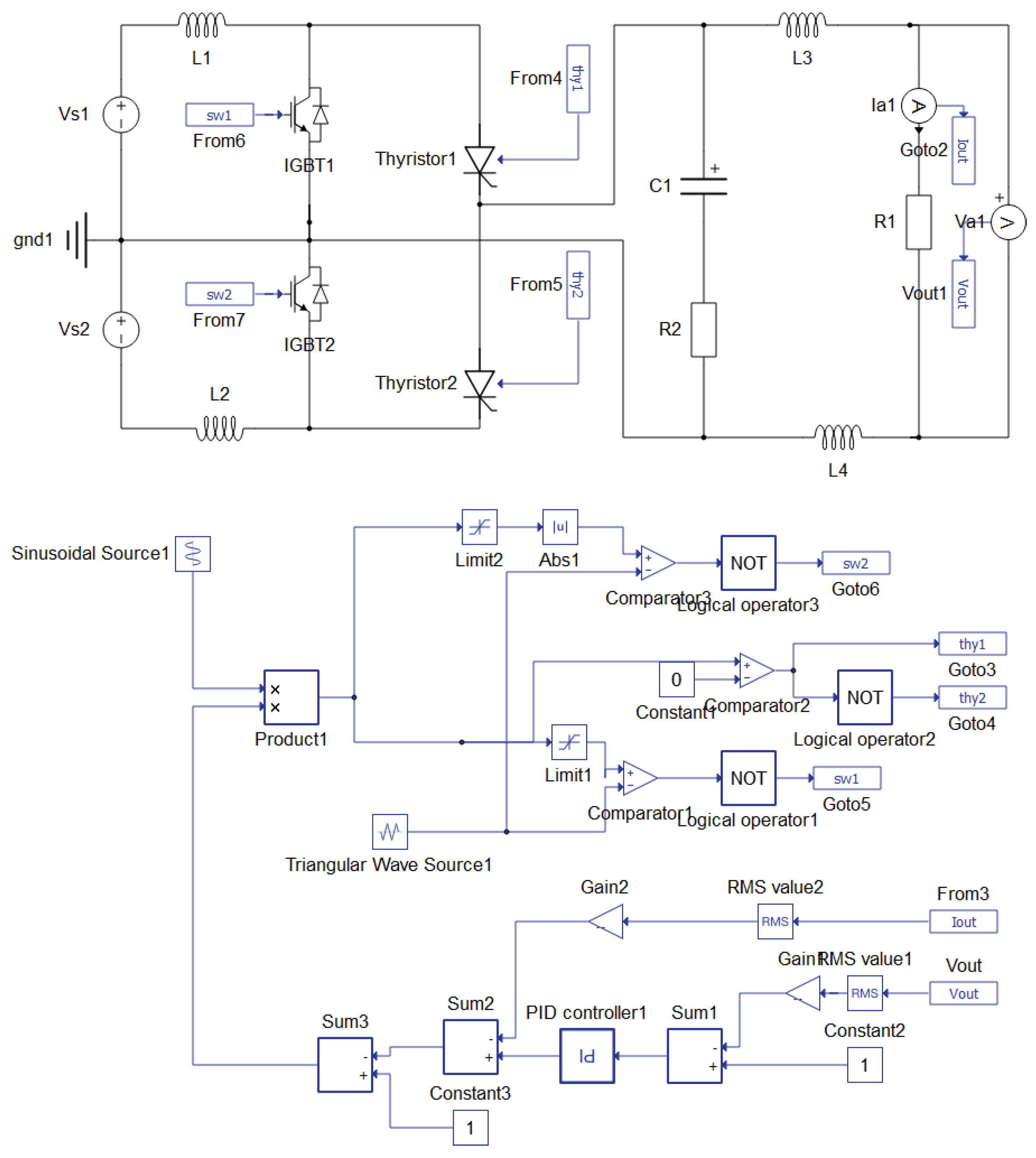
1.3. System Description
- Reduced switching loss due to single switch modulation, which also leads to zero current switchings for thyristors;
- the current through the SCR drops below the value of the holding current naturally and prevents crossover distortion;
- low component count in the main current path. This topology does not include series diodes with SCRs to block reverse voltages. In addition, SCRs do not require any snubber circuit as they commutate naturally due to the waveshaper output current.
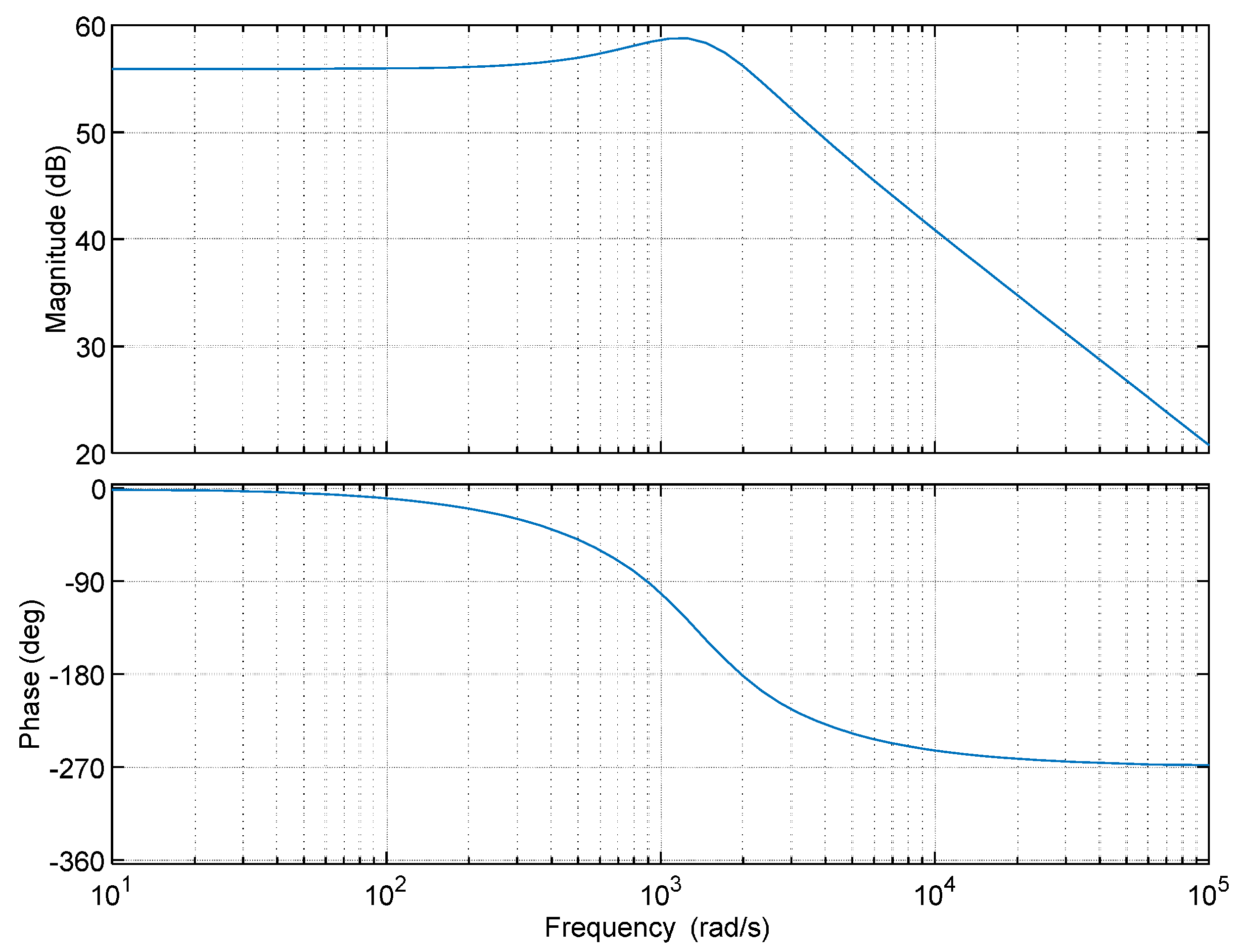
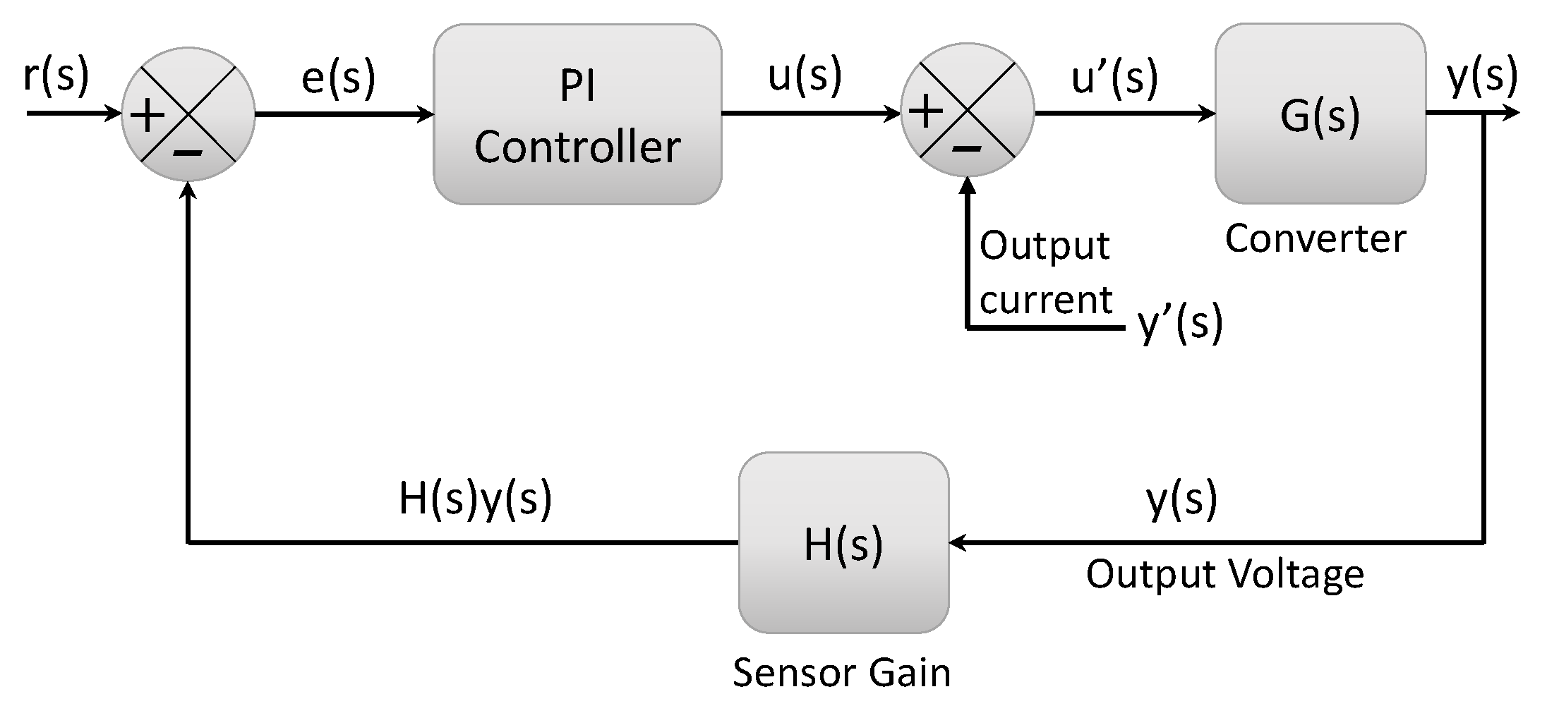
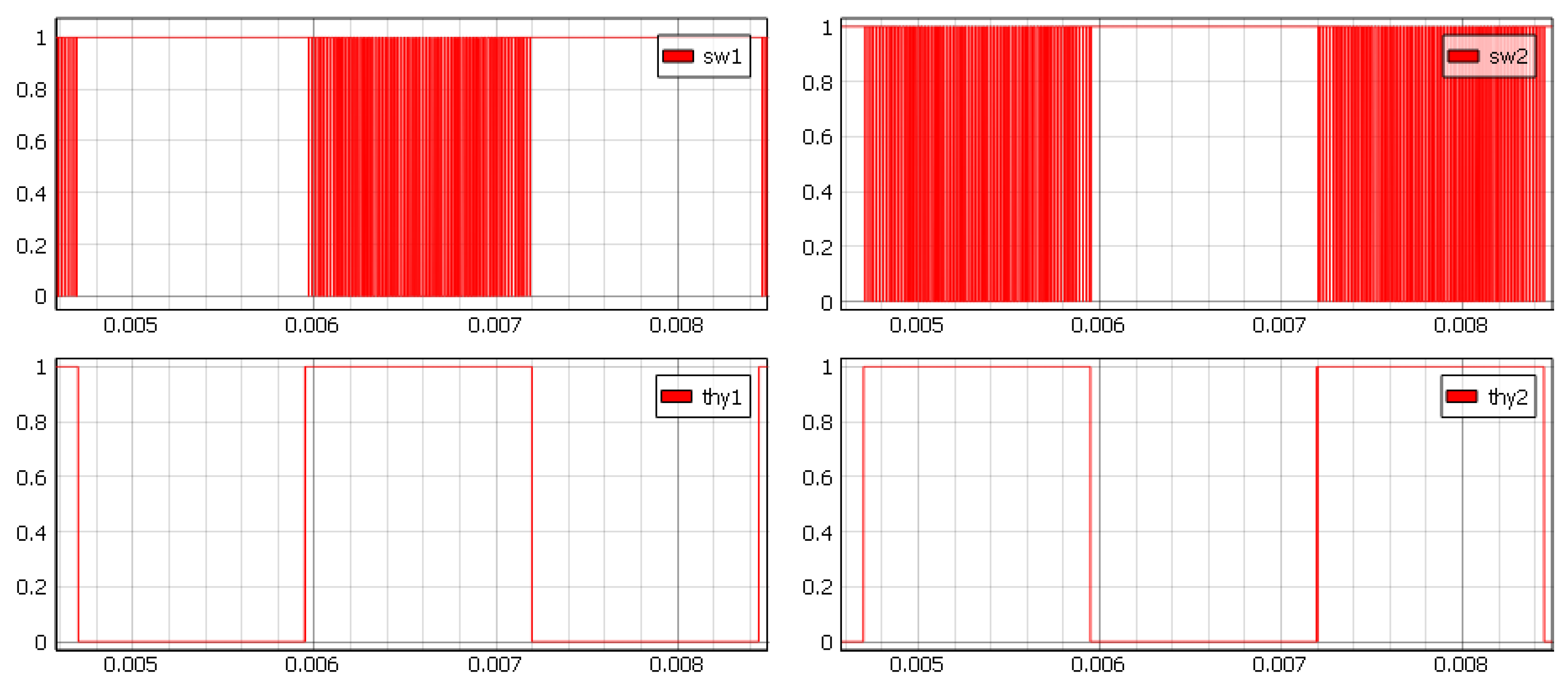
1.4. Control Scheme
2. Inverter Simulations
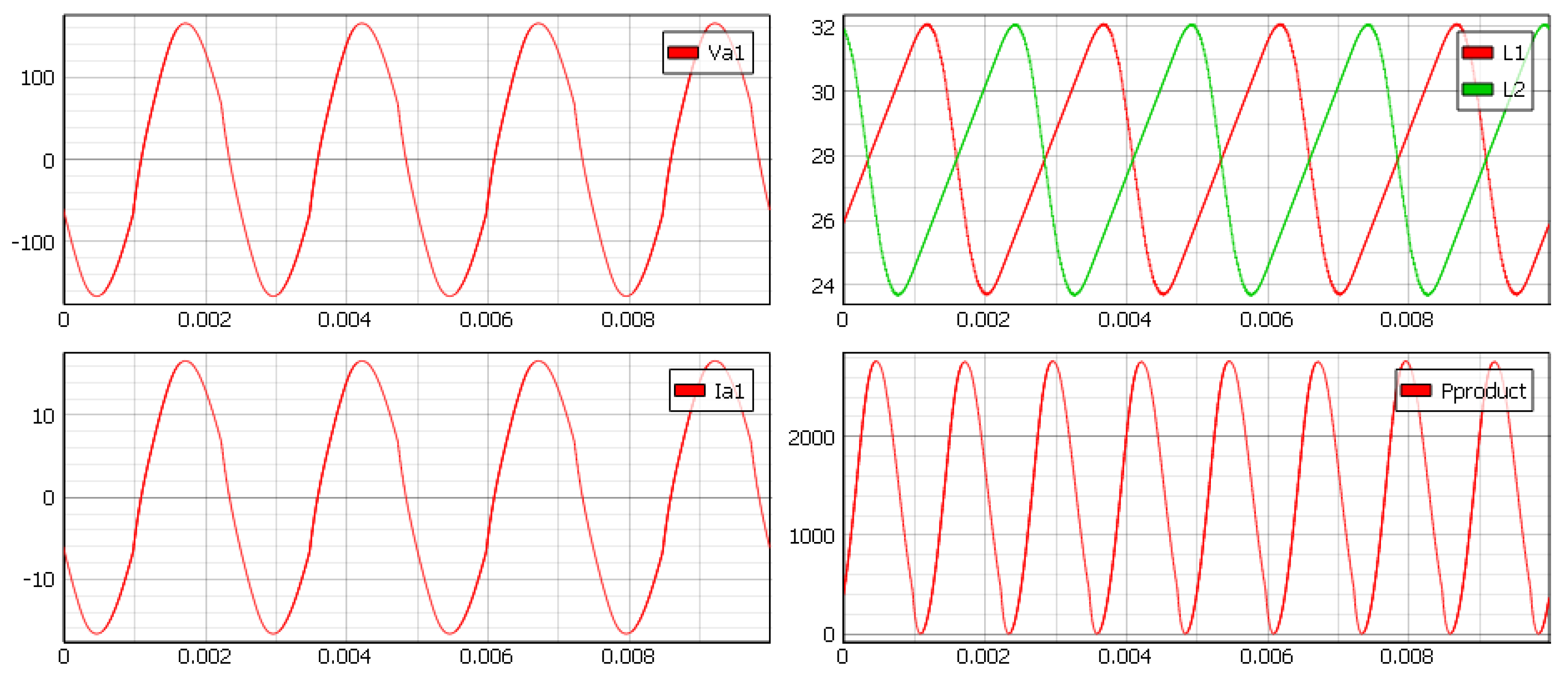
2.1. Ideal Operation Test
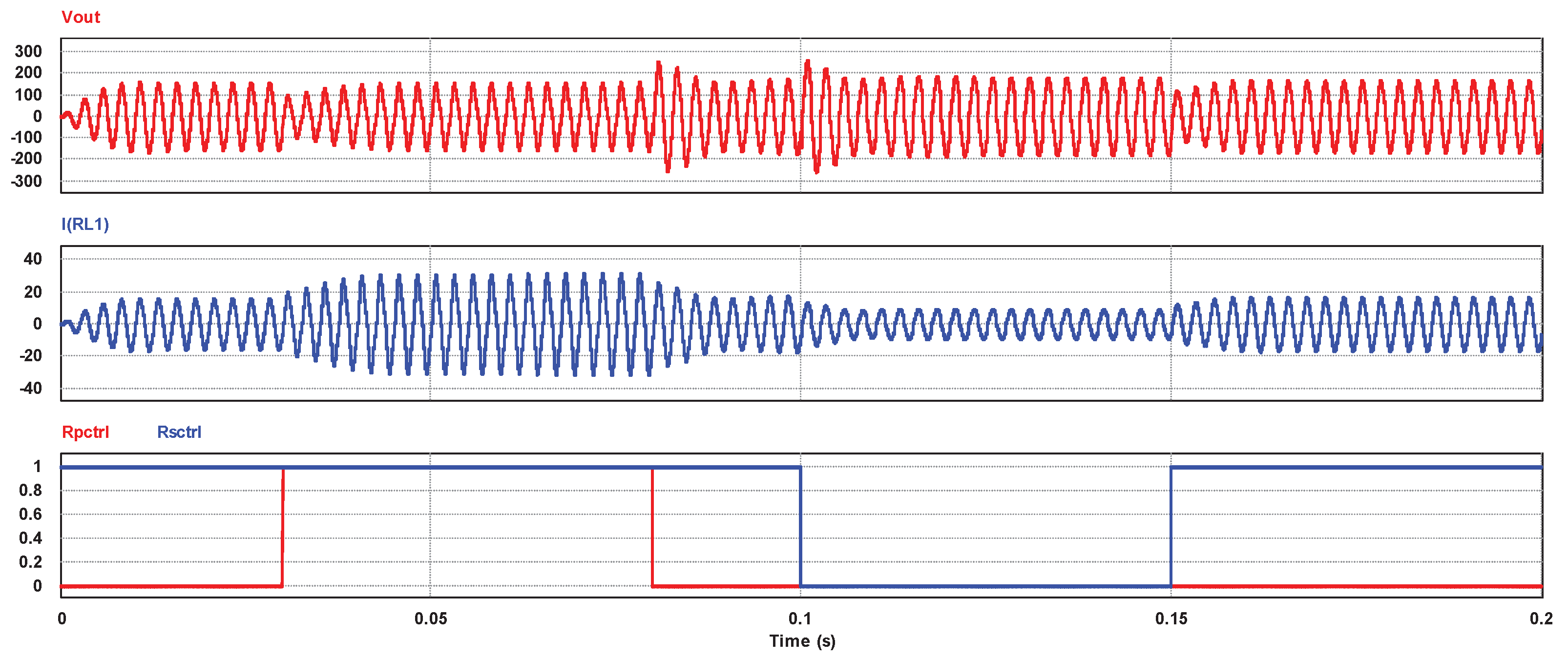
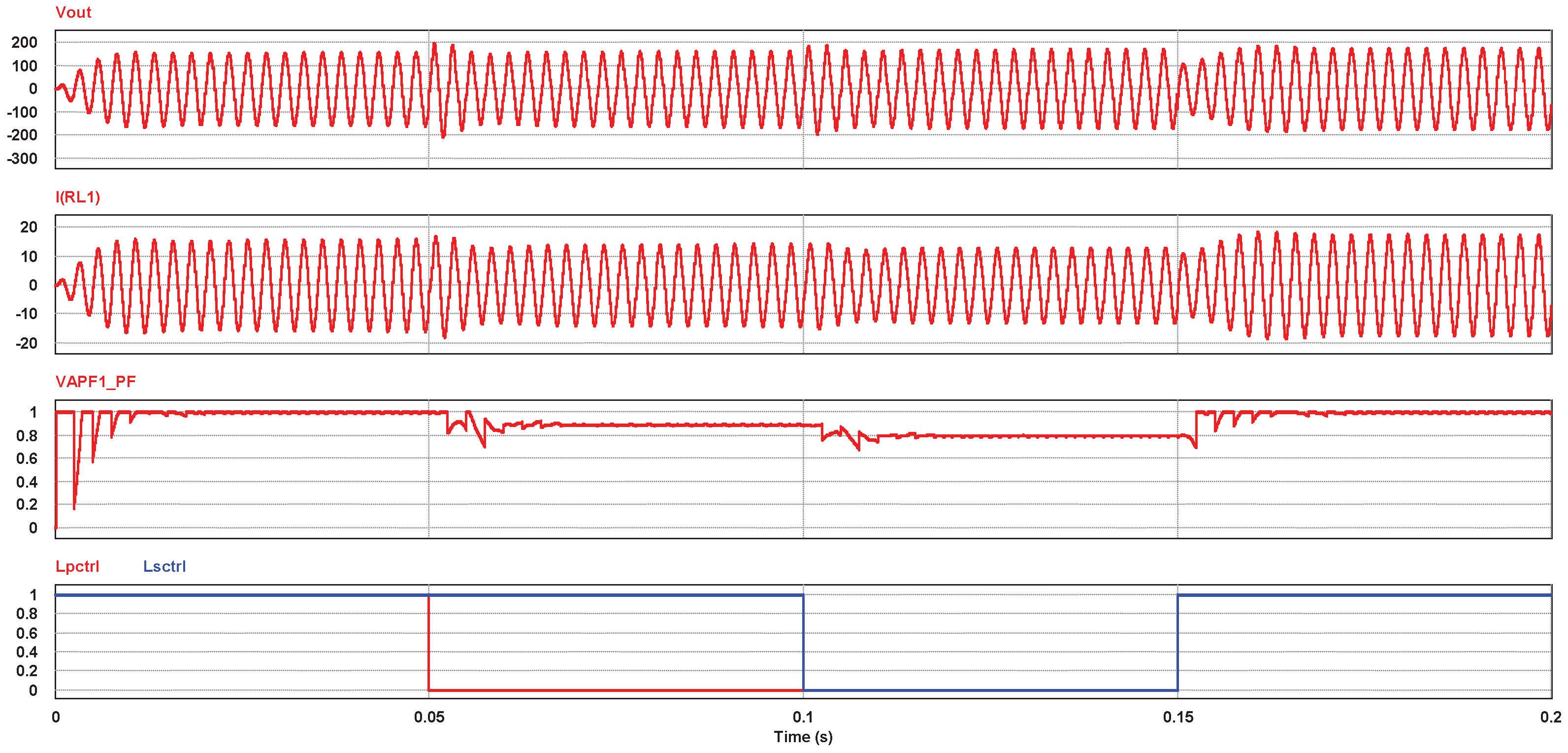
2.2. Dynamic Load Test
3. Experimental Results
Test Procedure
4. Conclusions
Author Contributions
Funding
Institutional Review Board Statement
Informed Consent Statement
Data Availability Statement
Conflicts of Interest
Abbreviations
| AC | Alternating current |
| AEA | All electric aircraft |
| CL | Capacitor inductor |
| CSI | Current–source inverter |
| DC | Direct current |
| DC/DC | Direct current to direct current converter |
| DC/AC | Direct current to alternating current converter (inverter) |
| GaN | Gallium Nitride |
| HIL | Hardware-in-the-loop |
| IGBT | Insulated-gate bipolar transistor |
| MEA | More electric aircraft |
| MOSFET | Metal oxide semiconductor field effect transistor |
| PF | Power factor |
| PWM | Pulse width modulation |
| rms | Root mean square |
| SCR | Silicon controlled rectifier (thyristor) |
| SiC | Silicon carbide |
| THD | Total harmonic distortion |
| VSI | Voltage-source inverter |
References
- Rosero, J.A.; Ortega, J.A.; Alabadas, E.; Romeral, L. Moving towards a more electric aircraft. IEEE Aerosp. Electron. Syst. Mag. 2007, 22, 3–9. [Google Scholar] [CrossRef] [Green Version]
- Abarzadeh, M.; Kojabadi, H.M. A static ground power unit based on the improved hybrid active neutral-point-clamped converter. IEEE Trans. Ind. Electron. 2016, 63, 7792–7803. [Google Scholar] [CrossRef]
- Mihalache, L. DSP control of 400 Hz inverters for aircraft applications. In Proceedings of the IEEE Industry Applications Conference, Pittsburgh, PA, USA, 13–18 October 2002; pp. 1564–1571. [Google Scholar]
- Sener, E.; Ertasgin, G. Current-source 1-Ph inverter design for aircraft applications. Aircraft Eng. Aerosp. Technol. 2020, 92, 1295–1305. [Google Scholar] [CrossRef]
- Yuan, G.; Luo, S.; Zhou, S.; Zou, X.; Zou, K. Low-order harmonics analysis and suppression method for 400 Hz single-phase VSI. In Proceedings of the IEEE Applied Power Electronics Conference and Exposition, Charlotte, NC, USA, 15–18 March 2015; pp. 2341–2345. [Google Scholar]
- Khaligh, H.; Torkaman, H.; Ebrahimian, A. Novel algorithm for optimum output passive filter design in 400 Hz inverter. In Proceedings of the IEEE Annual Power Electronics, Drives Systems and Technologies Conference, Tehran, Iran, 13–15 February 2018; pp. 335–340. [Google Scholar]
- Jahns, T.M.; Maldonado, M.A. A new resonant link aircraft power generating system. IEEE Trans. Aerosp. Electron. Syst. 1993, 29, 206–214. [Google Scholar] [CrossRef]
- He, J.; Zhang, D.; Torrey, D. Recent advances of power electronics applications in more electric aircrafts. In Proceedings of the AIAA/IEEE Electric Aircraft Technologies Symposium, Cincinnati, OH, USA, 12–14 July 2018; pp. 1–8. [Google Scholar]
- Prisse, L.; Ferer, D.; Foch, H.; Lacoste, A. New power centre and power electronics sharing in aircraft. In Proceedings of the IEEE European Conference on Power Electronics and Applications, Barcelona, Spain, 8–10 September 2009; pp. 1–9. [Google Scholar]
- MIL-STD-704F; Aircraft Electric Power Characteristics. Department of Defense Interface Standard: Washington, DC, USA, 2004.
- Ertasgin, G.; Whaley, D.M.; Ertugrul, N.; Soong, W.L. Analysis of DC Link energy storage for single-phase grid-connected PV inverters. Electronics 2019, 8, 601. [Google Scholar] [CrossRef] [Green Version]
- Yao, Z.; Wang, Z.; Blaabjerg, F.; Loh, P.C. Single-Stage Doubly Grounded Transformerless PV Grid-Connected Inverter with Boost Function. IEEE Trans. Power Electron. 2022, 37, 2237–2249. [Google Scholar] [CrossRef]
- Alajmi, B.N.; Ahmed, K.H.; Adam, G.P.; Williams, B.W. Single-phase single-stage transformer less grid-connected PV system. IEEE Trans. Power Electron. 2013, 28, 2664–2676. [Google Scholar] [CrossRef]
- Cai, W.; Jiang, L.; Liu, B.; Duan, S.; Zou, C. A power decoupling method based on four-switch three-port DC/DC/AC converter in DC microgrid. IEEE Trans. Ind. Appl. 2015, 51, 336–343. [Google Scholar] [CrossRef]
- Aghaei, N.; Bizhani, H. Using fuzzy controller for improvement of power decoupling performance in PV systems. Int. J. Electron. 2020, 51, 376–389. [Google Scholar] [CrossRef]
- Basabi, S.T.; Farzanehfard, H. Novel transistor-less series power decoupling in conventional current source inverter for PV application. In Proceedings of the IEEE Power Electronics, Drive Systems, and Technologies Conference, Iran, Tehran, 4–6 February 2020; pp. 1–5. [Google Scholar]
- Shimizu, T.; Suzuki, S. A single-phase grid-connected inverter with power decoupling function. In Proceedings of the IEEE International Power Electronics Conference, Sapporo, Japan, 21–24 June 2010; pp. 2918–2923. [Google Scholar]
- Hirachi, K.; Tomokuni, Y. A novel control strategy on single–phase PWM current source inverter incorporating pulse area modulation. In Proceedings of the IEEE Power Conversion Conference, Nagaoka, Japan, 3–6 August 1997; pp. 289–294. [Google Scholar]
- Li, R.T.H.; Chung, H.S.; Chan, T.K.M. An active modulation technique for single-phase grid-connected CSI. IEEE Trans. Power Electron. 2007, 22, 1373–1382. [Google Scholar] [CrossRef]
- Kyritsis, A.C.; Papanikolaou, N.P.; Tatakis, E.C. A novel parallel active filter for current pulsation smoothing on single stage grid-connected AC-PV modules. In Proceedings of the IEEE European Conference on Power Electronics and Applications, Aalborg, Denmark, 2–5 September 2007; pp. 1–10. [Google Scholar]
- Zhang, J.; Ding, H.; Wang, B.; Guo, X.; Padmanaban, S. Active Power Decoupling for Current Source Converters: An Overview Scenario. Electronics 2019, 8, 197. [Google Scholar] [CrossRef] [Green Version]
- Watanabe, H.; Itoh, J.I. Novel DC to single-phase AC isolated current source inverter with power decoupling capability for micro-inverter system. In Proceedings of the IEEE Energy Conversion Congress and Exposition, Aalborg, Denmark, 20–24 September 2015; pp. 158–165. [Google Scholar]
- Lin, B.R.; Wang, K.W. Interleaved soft switching resonant converter with a small input ripple current. Int. J. Electron. 2020, 107, 644–658. [Google Scholar] [CrossRef]
- Tarter, R.E. Current-fed converters. In Solid-State Power Conversion Handbook, 1st ed.; Wiley-Interscience: New York, NY, USA, 1993; pp. 429–433. [Google Scholar]
- Madonna, V.; Migliazza, G.; Giangrande, P.; Lorenzani, E.; Buticchi, G.; Galea, M. The rebirth of the current source inverter: Advantages for aerospace motor design. IEEE Ind. Electron. Mag. 2019, 13, 65–76. [Google Scholar] [CrossRef]
- Mazda, F. The current-fed inverter. In Power Electronics Handbook, 3rd ed.; Newnes: Oxford, UK, 1997; pp. 345–350. [Google Scholar]
- Xiong, Y.; Oyane, A.; Ou, T.; Thilak, S.; Imaoka, J.; Yamamoto, M. Comparison of switching performance between GaN and SiC MOSFET via 13.56 MHz Half-bridge Inverter. In Proceedings of the IEEE International Symposium on Industrial Electronics, Delft, The Netherlands, 17–19 June 2020; pp. 672–676. [Google Scholar]
- Kamli, M.; Yamamoto, S.; Abe, M. A 50–150 kHz half-bridge inverter for induction heating applications. IEEE Trans. Ind. Electron. 1996, 43, 163–172. [Google Scholar] [CrossRef]
- Wang, X.; Loh, P.C.; Blaabjerg, F. Stability analysis and controller synthesis for single-loop voltage-controlled VSIs. IEEE Trans. Power Electron. 2017, 32, 7394–7404. [Google Scholar] [CrossRef] [Green Version]
- Wang, X.; Li, Y.W.; Blaabjerg, F.; Loh, P.C. Virtual-impedance - based control for voltage-source and current-source converters. IEEE Trans. Power Electron. 2015, 30, 7019–7037. [Google Scholar] [CrossRef]
- IEEE Standard 519-2014; IEEE Recommended Practice and Requirements for Harmonic Control in Electric Power Systems. IEEE-SA Standards Board: Piscataway, NJ, USA, 2014.
- Ertasgin, G.; Soong, W.L.; Ertugrul, N. Analysis and design of single-phase current-source grid-connected PV inverter. In Proceedings of the IEEE European Conference on Power Electronics and Applications, Lille, France, 2–6 September 2013; pp. 1–10. [Google Scholar]


| Steady State Characteristics | Limits |
|---|---|
| Voltage | 108.0 to 118.0 V, rms |
| Voltage Unbalance | 3.0 V, rms max. |
| Voltage Modulation | 2.5 V, rms max. |
| Voltage Phase Difference | 116 to 124 |
| Distortion Factor | 0.05 max. |
| Crest Factor | 1.31 to 1.51 |
| DC Component | +0.10 to −0.10 V |
| Frequency | 393 to 407 Hz |
| Peak Voltage | ±271.8 V |
| Controller Type | ||
|---|---|---|
| PI | 0.45 | 1.2 |
| Parameter | Value |
|---|---|
| Input Voltage | 56 V |
| Input Current | 26 A |
| Output Voltage | 120 V rms |
| Output Current | 12 A rms |
| Output Power | 1.4 kW |
| DC link Inductors (, ) | 5 mH |
| Filter Inductors (, ) | 600 H |
| Filter Capacitor () | 20 F |
| Switching Frequency | 50 kHz |
| Parameter | Value |
|---|---|
| Output Voltage () | 120 V rms |
| Output Current () | 12 A rms |
| Output Frequency | 400 Hz |
| Crest Factor | 1.43 |
| Output Power () | 1440 W |
| Input Power () | 1512 W |
| Efficiency (%) | 98 |
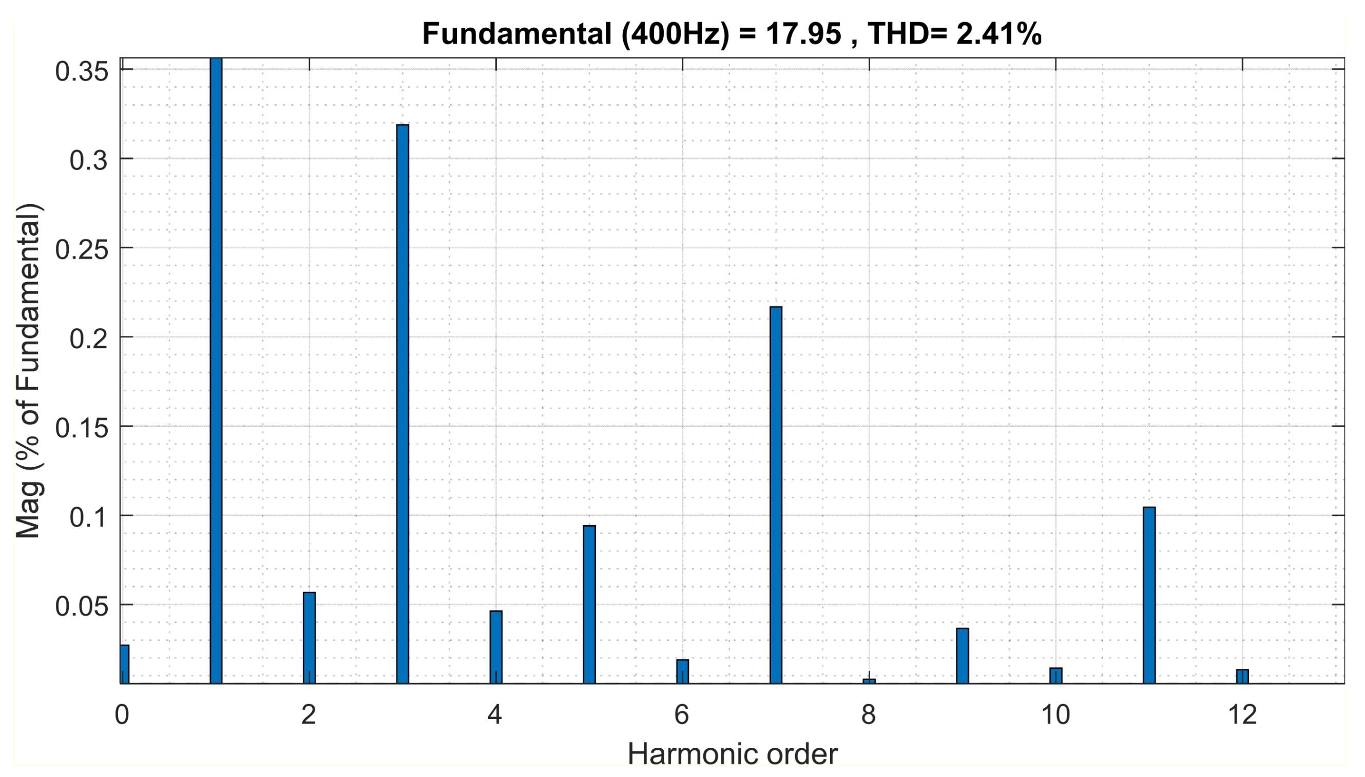
| THD (%) | 2.41 |
Publisher’s Note: MDPI stays neutral with regard to jurisdictional claims in published maps and institutional affiliations. |
© 2022 by the authors. Licensee MDPI, Basel, Switzerland. This article is an open access article distributed under the terms and conditions of the Creative Commons Attribution (CC BY) license (https://creativecommons.org/licenses/by/4.0/).
Share and Cite
Sener, E.; Ertasgin, G. Design of a Half-Bridge Current-Source Inverter Topology for Avionic Systems. Aerospace 2022, 9, 354. https://doi.org/10.3390/aerospace9070354
Sener E, Ertasgin G. Design of a Half-Bridge Current-Source Inverter Topology for Avionic Systems. Aerospace. 2022; 9(7):354. https://doi.org/10.3390/aerospace9070354
Chicago/Turabian StyleSener, Eralp, and Gurhan Ertasgin. 2022. "Design of a Half-Bridge Current-Source Inverter Topology for Avionic Systems" Aerospace 9, no. 7: 354. https://doi.org/10.3390/aerospace9070354