
Radiation Dose Detection on FY-4B Satellite
by
 , , ,
, , ,
Ying Sun
1,2,3,*, 
Binquan Zhang
1,3,
Xiaoxin Zhang
4,5,
Guohong Shen
1,3,
Tao Jing
1,2,3,
Shenyi Zhang
1,2,3,
Xianguo Zhang
1,3,
Cong Huang
4,5,
Jiawei Li
4,5,
Weiguo Zong
4,5,
Xin Zhang
1,3 and
Huanxin Zhang
1,3
1
National Space Science Center, Chinese Academy of Sciences, Beijing 100190, China
2
University of Chinese Academy of Sciences, Beijing 100049, China
3
Beijing Key Laboratory of Space Environment Exploration, Beijing100190, China
4
National Center for Space Weather, China Meteorological Administration, Beijing 100081, China
5
Innovation Center for FengYun Meteorological Satellite (FYSIC), Beijing 100081, China
*
Author to whom correspondence should be addressed.
Aerospace 2023, 10(4), 325; https://doi.org/10.3390/aerospace10040325
Submission received: 20 February 2023
/
Revised: 16 March 2023
/
Accepted: 22 March 2023
/
Published: 24 March 2023
(This article belongs to the Special Issue Meteorological Satellites Data Analysis)
Abstract
:The radiation damage effect is relatively serious during spacecraft operation in orbit. To know the real cumulative dose in orbit accurately, a radiation dose detector is carried on the FY-4B satellite. It comprises one electric control unit and three dose detectors, with a total of four payloads. Each dose detector includes five dose-monitoring points corresponding to different shielding thicknesses, which are mainly used for the measurement of the dose depth. Three dose detectors with the same function are installed in the X, Y and Z positions and can detect the total dose in different directions during the operation of the satellite. Each detector has the characteristics of small size, high integration and low power consumption. At present, the FY-4B satellite is in orbit. The detectors have been working normally since they were started up, and good preliminary detection results have been obtained. From the power-up of the detectors to April 2022, the maximum dose has reached 2.7 × 10³ rad(Si). We conducted a preliminary analysis of the relationship between total dose and shielding thickness. In addition, the relationship between daily average dose and shielding thickness was further analyzed. These studies have application value for radiation protection design.
1. Introduction
The FY-4 satellites are the second generation of China’s geostationary meteorological satellite. It is an ideal platform for space environment monitoring. The satellite is affected by various space environmental effects during its operation, such the single-event effect, charge–discharge effect and radiation damage effect. These effects can sometimes cause a serious impact on the satellite. Therefore, for safe operation and possible fault analysis, satellites carry relevant detectors for space environmental effect monitoring. The monitoring of the space radiation dose is an important means to ensure the safe operation of satellites. Accurate acquisition of the total radiation dose suffered by a satellite during operation is significance for the evaluation and analysis of the satellite’s working state.
As early as 1984, American scientists August and Circle carried out research on detecting the total radiation dose with a PMOS dosimeter [1]. The PMOS dosimeter usage was compared to other dosimeters, such as the CaF2:Mn thermoluminescent dosimeter and the radiachromic nylon film dosimeter, and the research showed that it is more convenient and faster to detect the dose with a PMOS dosimeter. Kelleher et al. introduced a design approach that could increase the sensitivity of the PMOS dosimeter [2]. Next, the space application of PMOS total dose detection gradually increased [3,4,5,6,7]. These results showed that PMOS is a good choice for a low dose rate and total dose space application. China first detected the space dose in 1999 and also adopted PMOS technology [8]. After years of technical improvement, people realized that the monitoring results of the space dose have good application value for the radiation protection design of follow-up satellites. So, total radiation dose detection technology has been widely used [9].
In view of the seriousness of the cumulative radiation effect of the space charged particle irradiation environment on the satellite and its payloads, the space environment monitoring subsystem of the FY-4B satellite is equipped with a radiation dose detector. This detector shows good innovation in detection technology. The accumulated dose under different shielding thicknesses in orbit can be measured and analyzed. The detection data are more sufficient and accurate and have good research value. This paper focuses on the engineering implementation of the radiation dose detector and the analysis of preliminary detection results in orbit.
2. Instrument Functions and Engineering Constraints
2.1. Instrument Function and Index
The radiation dose detector includes one electric control unit and three dose detectors. The electric control unit provides the required secondary power supply for the three dose detectors, and it is also responsible for the acquisition and transmission of detection data. The three dose detectors cover the X, Y and Z directions of the satellite. Each detector contains five dose detection points. Each dose detection point uses a PMOS sensor. There are electronic circuits at the back end to process the five sensor signals. The five PMOS sensors correspond to five kinds of shielding thickness. Therefore, the monitoring of the space radiation dose under different shielding thicknesses can be realized in orbit. The total dose in different directions in the satellite is detected, and the dose depth distribution is studied at the same time. See Table 1 for the main technical indexes of the irradiation dosimeter. According to the design requirements, different detection points correspond to different detection ranges. The detection sensitivity of each detection point is also different. We named the five dose detection points D1 to D5.
2.2. Engineering Constraints
The payloads adopt a miniaturization design, which has the characteristics of small volume, high integration and low power consumption. Detailed engineering indexes are shown in Table 2. The power consumption of a single dose detector is less than 0.65 W. The total power consumption of four loads is less than 3.35 W. The weight of each load is 0.8 kg, and the total weight of four loads is about 3.2 kg. The engineering structures and functions of the three dose detectors are completely the same, which are installed inside the satellite and connected with the electric control unit through cables.
3. Engineering Realization
3.1. Overall Scheme
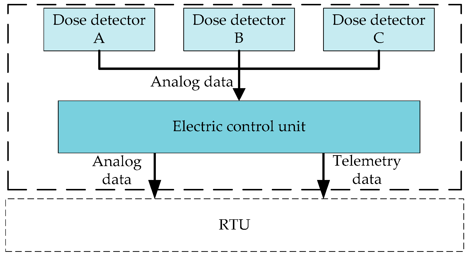
The FY-4B satellite radiation dose detector consists of one electric control unit and three dose detectors. See Figure 1 for the composition block diagram. The electric control unit inputs a primary power supply of +28 V from the RTU and converts it into +15 V to provide the required secondary power supply for the dose detectors. In addition, the electric control unit is also responsible for the collection and transmission of dose detection data to the RTU. The RTU controls the switch of the radiation dose detector. The radiation dose detector is equipped with three dose detectors installed in different directions of the satellite. Each dose detector has five dose-monitoring points corresponding to five different shielding thicknesses. The appropriate specifications and models of PMOS are selected as sensors for total dose detection. According to the ground simulation calculation results, the range design of the five sensors of each detector is 2 × 10⁶ rad(Si), 4 × 10⁵ rad(Si), 4 × 10⁴ rad(Si), 2 × 10⁴ rad(Si), and 8 × 10³ rad(Si), respectively. The measurement range can meet the total mission requirements of the satellite in orbit life. The PMOS sensors on the detector measure the cumulative radiation dose, and then the detection data are processed by the electric control unit, digitized by the RTU, and packaged and transmitted to the satellite platform.
3.2. Sensor Selection
Detecting the space radiation dose with a PMOS sensor is widely used in the world. A PMOS is a radiation-sensitive field effect transistor made with a specific process. When it is irradiated, an oxide trap charge and an interface trap charge are generated in its oxide layer, which makes the gate voltage drift. The relationship between gate voltage offset and irradiation cumulative dose can be obtained with calibration. The working principle of the radiation dose detector is to use this correspondence to monitor the change in the gate voltage so as to know the radiation dose of the sensor.
The gate oxide layer is the main sensitive area of the PMOS sensor. The bigger the thickness of the gate oxide layer, the much more irradiated is the ionized electron–hole that can be captured by the defects in the oxide layer, and the greater is the change in the gate voltage drift. So, the PMOS sensor with a thicker gate oxide layer has higher sensitivity. With the increase in the total irradiation dose, the gate voltage of the PMOS sensor drifts in the negative direction, that is, the gate voltage becomes smaller [10].
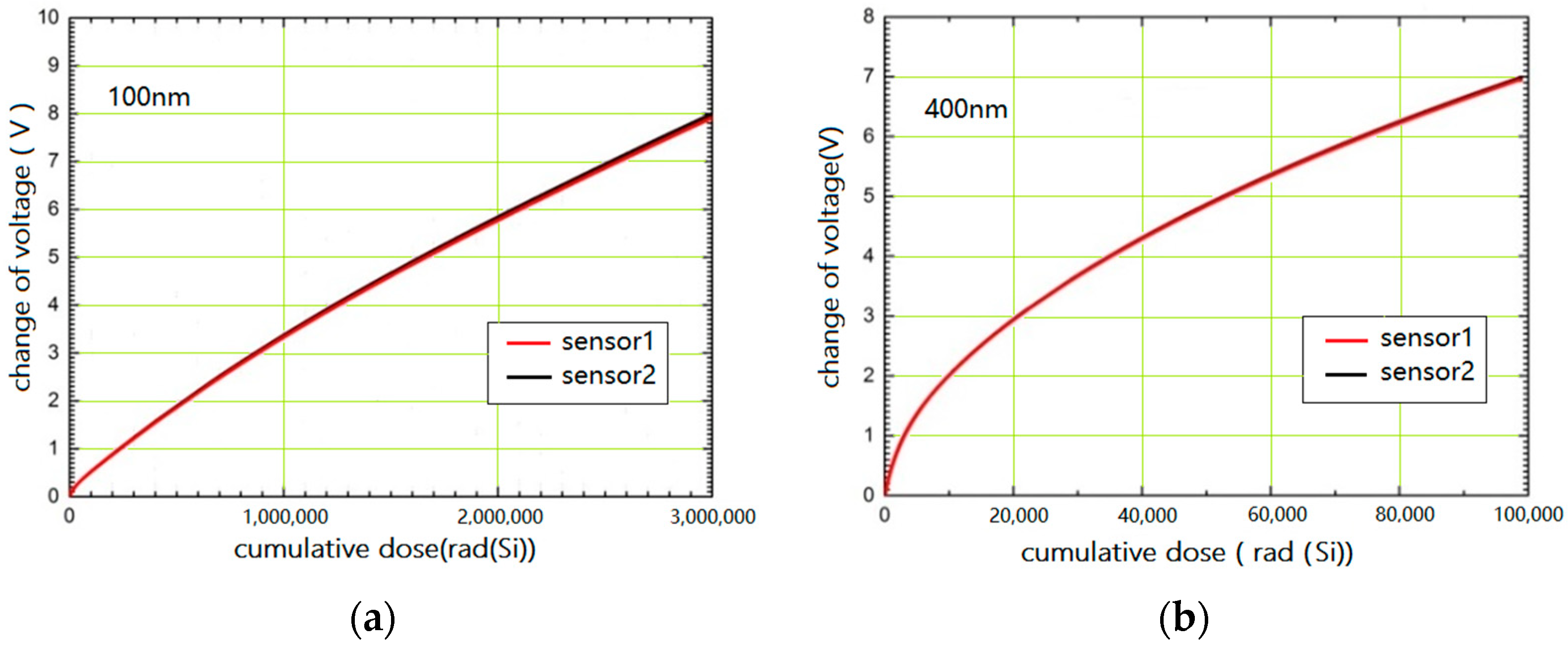
The thickness of the PMOS gate oxide layer can be 100 nm, 400 nm or 1 um. In this satellite task, we selected two kinds of sensors with a thickness of 100 nm and 400 nm. The measurement range of the 100 nm PMOS sensor is larger, but the detection sensitivity is low. The detection range of the 400 nm PMOS sensor is smaller, but the detection sensitivity is high. The relationship curves of the output voltage of PMOS sensors with the dose are shown in Figure 2. According to the detection index requirements of the FY-4B satellite, combined with the characteristics of different dose detections of PMOS sensors, the 400 nm PMOS sensor is chosen for the dose detection points of D1, D4 and D5. It can meet the detection requirement of high accuracy. The 100 nm PMOS sensor is chosen for the dose detection points of D2 and D3. It can meet the detection requirement of a large range.
3.3. Electronics Design
The irradiation dosimeter mainly includes two parts, which are electronic control unit electronics and dose detector electronics. The electronic principle diagram of the dose detector is shown in Figure 3.
The electronics of the electric control unit is composed of a secondary power conversion module, a power test module, a signal acquisition module and a temperature test module. It can provide secondary power for the three dose detectors and realize the collection and transmission of detector signals. As an engineering parameter, the power test module output can be used as the basis for judging whether the radiation dose detector works normally. In the power module circuit, the noise suppression circuit is selected. The back end of the DC/DC power converter is connected with an electromagnetic interference filter.
Dose detector electronics is mainly composed of a PMOS sensor circuit, a constant current source circuit, a comparison sampling circuit, a signal amplification output circuit and a temperature test circuit. There are two circuit boards. Five PMOS sensors and two temperature test circuits are designed on one circuit board, and the other circuits are designed on the other circuit board. The two circuit boards are electrically connected through electrical connectors between boards. The PMOS circuit is the main radiation receiving board. PMOS sensors are sensitive to temperature. To know about the working temperature environment of the PMOS sensors more accurately, two temperature-monitoring points are set on the sensor circuit board. The in-orbit temperature data can be used for the correction of dose detection data to improve data accuracy.
The other circuit board includes a constant current source circuit, a comparison sampling circuit and a signal amplification output circuit. This circuit board is placed behind the PMOS circuit board. It can prevent other circuit components from receiving radiation and affecting device performance. In addition, we also added a corresponding radiation shielding design in the structure, which will be described in detail in the later structure design.
The constant current source circuit provides a stable current source for the PMOS sensors. The current needed by the 400 nm PMOS sensor is about 10μA, and the current needed by the 100 nm PMOS sensor is about 175μA. The current of the same model PMOS sensors is slightly different. We need to test each sensor to get the accurate current. Generally, we call this current the zero-temperature coefficient. The PMOS sensor is a p-channel enhanced MOSFET. We tested the I–V characteristic of the PMOS sensor at different temperatures and obtained I–V curves. The current value corresponding to the intersection of these curves is the zero-temperature coefficient point. The test of the zero-temperature coefficient needs to select at least four constant temperature points within the range of −25 °C to +55 °C for testing. The PMOS working at this current point has the least temperature effect.
The response signal of the sensor after receiving irradiation is processed and amplified by the comparison sampling circuit and the amplification output circuit and finally output to the electric control unit. Through the design and debugging of the dose detector circuit, the task index requirements of the dose detection range and sensitivity are realized.
3.4. Detector Structure
To measure the cumulative dose under different shielding thicknesses, five sensors are designed for each dose detector, and the shielding thickness of each sensor is different [11]. The front panel of the five sensors is Al hemispherical structures with five kinds of thickness. The PMOS sensor is located at the center of the hemispherical structures. Figure 4 shows a three-dimensional picture with local transparency. From this figure, we can see that there are two circuit boards in the casing, and the left one is a PMOS board. The PMOS board is close to the front panel, which can ensure that the sensors are in the center of the hemisphere as much as possible and also ensure the detection field of view.
Three cylindrical shielding structures are installed on the back of the PMOS board, as shown by the yellow objects in Figure 4. The shielding structures are made of copper with a thickness of 1 mm. The density of copper is 8.96 g/cm3, which is more than three times the Al density. The installation position corresponds to the thinner position of the front panel. The shielding structures can effectively protect the right circuit board from radiation.
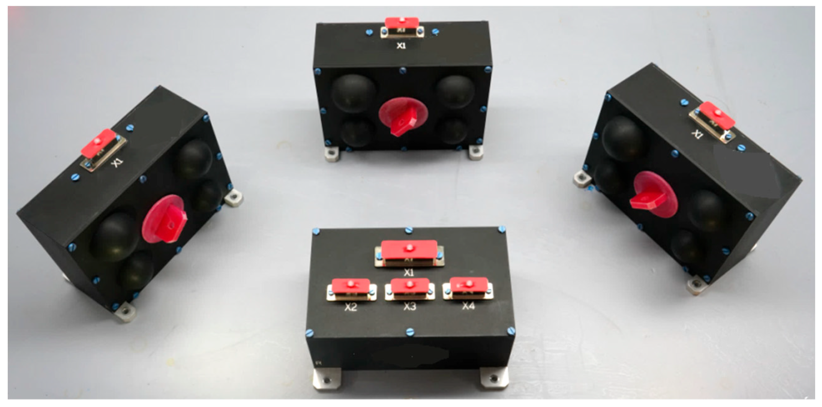
The structure of both the electronic control unit and dose detectors comprises an intermediate main structure and a side panel. The main structure adopts integrated molding. The circuit boards are fixed inside the main structure. The side panel is fastened to the main structure with screws. This structural design has the advantages of simple installation and strong anti-vibration ability. A photograph of the radiation dose detector is shown in Figure 5. The shell of the detector is made of 2A12 duralumin alloy, and the surface is treated with black anodizing. The red parts are protective covers, which were removed when the payloads were installed in the satellite.
4. Detector Calibration
4.1. Calibration Test
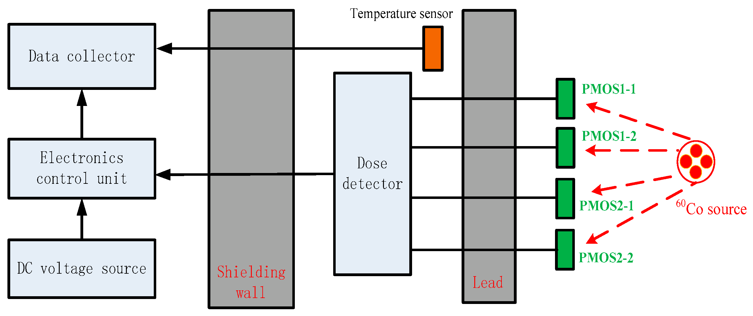
A radiation source was used to irradiate the PMOS sensors in a dose standard laboratory. The output signals of the sensors were generated, transmitted to the electric control unit and collected and analyzed with a data acquisition system. During the test, the circuit was shielded with lead brick to reduce the impact of radiation. Only the PMOS sensors were irradiated. The calibration test scheme is shown in Figure 6. The radioactive source was 20,000 Curies of 60Co from the Xinjiang Technical Institute of Physics and Chemistry, CAS. The average energy of the radiation source was 1.25 MeV, and the dose rate of the radiation source was calibrated. During the calibration test, it was necessary to record the dose rate at the sensor position, the start and end times of irradiation, the output voltage and ambient temperature of the dosimeter at different times, etc. The total dose of the irradiation test was bigger than the design range of the dosimeter, so we could judge whether the output of the dosimeter was normal at the maximum range.
We needed to know whether the 100 nm PMOS and 400 nm PMOS sensors were tested. The dose rate for the 100 nm PMOS sensor was 51.63 rad(Si)/s. The dose rate for the 400 nm PMOS sensor was 1.225 rad(Si)/s. Therefore, we usually need several days to complete the calibration test, and the data are collected in real time, once a second, so as to facilitate the accuracy of later data analysis.
The PMOS sensors cannot be recovered after being irradiated, so the calibrated sensors can no longer be used for flight products. To ensure that the calibration results are applicable to the sensors used in the payload, we took measurements during the purchase, screening and testing of the sensors to ensure the performance of the calibration sensors was consistent with that of the flight sensors. First, during the selection of sensors, the products purchased were from the same manufacturer and underwent the same process. The models and production batches of the sensors used in the flight production were the same as those used in the ground calibration so as to ensure the consistency of sensor performance from the manufacturing source. Second, the purchased sensors were strictly screened. These tests included a high-temperature stability test, a zero-temperature coefficient point test, a high- and low-temperature power-on test and a room-temperature power-on test. Only sensors that have passed all the tests can be qualified and used in the calibration test and flight products. Finally, each batch of sensors was calibrated. In the calibration test, four 400 nm and 100 nm PMOS sensors were randomly selected from all the sensors for the test to verify the consistency of the sensor response.
4.2. Calibration Results
The aim of calibration is to determine the functional relationship between the gate voltage of the PMOS sensor and the irradiation cumulative dose. According to the calibration results of the sensors and the working parameters of the circuit, the total detection range of the dose detector can be obtained. The accuracy is obtained using the deviation between the measured value of the irradiation experiment and the actual value of the irradiation. Deviation refers to the difference between the test result of a certain dose value and the true value. The real value of the radiation source dose has been calibrated by the Chinese Academy of Metrology, and the test uncertainty is better than 0.1%. The PMOS sensor is frontally irradiated by the radiation source so as to avoid the error caused by the difference in the radiation direction.
The sensitivity of the sensor to irradiation of charged particles is high. So, detection sensitivity mainly depends on the minimum variation voltage of the payload. The detection data are 0 to 10 V analog output, which is composed of 15 bits. The lowest bit represents the detection sensitivity. The 10 V analog output is divided into 32,768 parts, so the minimum variation voltage is about 0.3 mV. That is, from the initial voltage after the payload is started up, each increase of 0.3 mV increases the corresponding irradiation dose, which is the sensitivity of the payload.
After the sensor is irradiated, the functional relationship between the change in the gate voltage output and the irradiation cumulative dose is as follows:
Y = A1·X + A2·X2 + A3·X3
Y is the irradiation dose value. X is the change of sensor gate voltage. A1, A2 and A3 are the conversion parameters. Through the analysis of calibration data, we obtained the conversion parameters’ value for the 400 nm and 100 nm sensors, as shown in the following Table 3.
First, we divided 0.3 mV by the amplification factor of the sensor analog circuit. This is the value of X. Next, through the functional relationship, we obtained the value of Y, which is the dose detection sensitivity of this sensor. The corresponding relationship between gate voltage and irradiation dose is nonlinear, and we selected the maximum value as the sensitivity.
5. Preliminary Detection Results
The radiation dose detector can detect the radiation dose generated by all charged particles, including primary particles and secondary particles. It cannot detect neutrons directly, but it can detect secondary particles produced by neutrons and obtain the cumulative dose. Its main function is to detect the total cumulative dose, without the ability of particle identification.
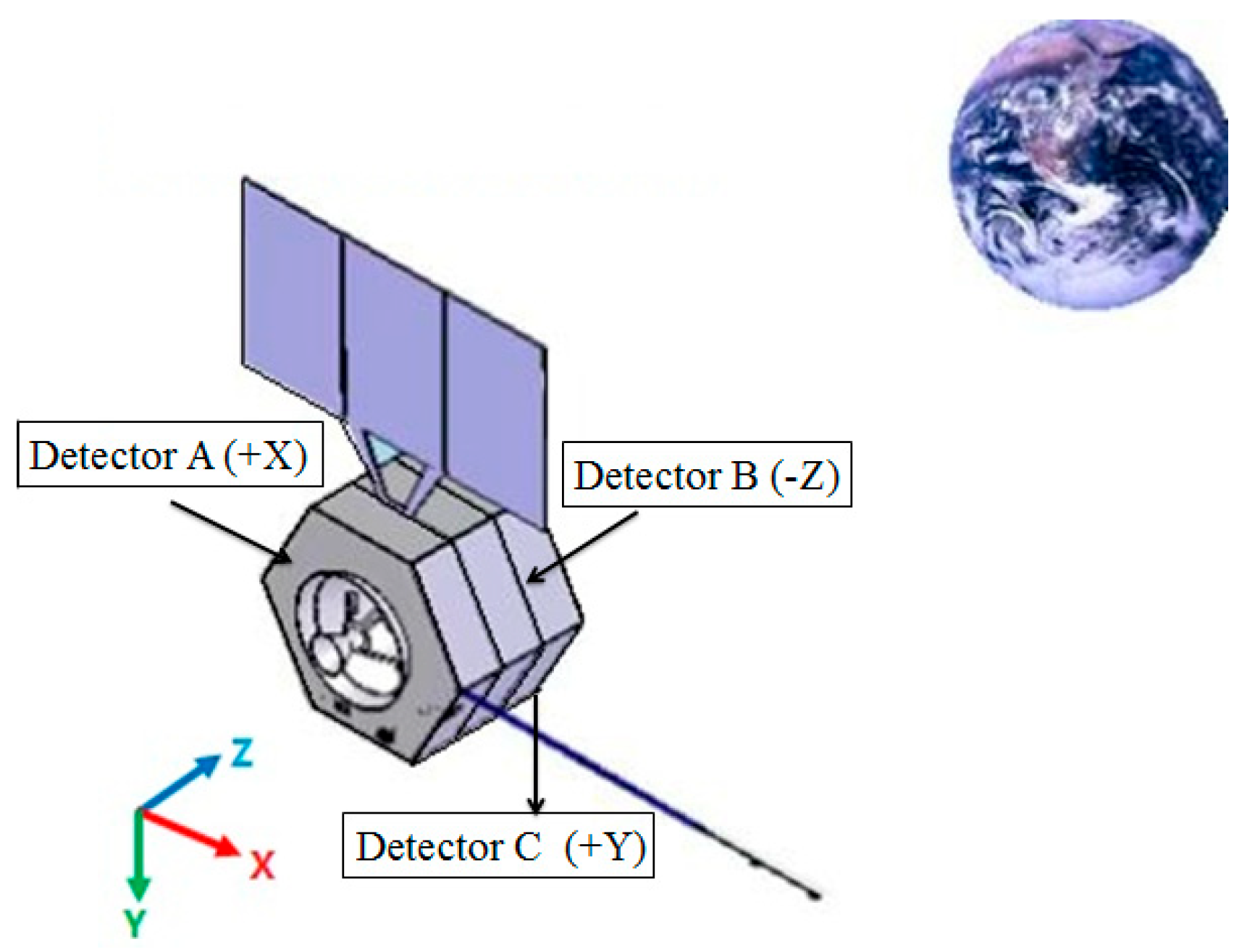
The FY-4B satellite was successfully positioned in the geostationary orbit over the equator at 123.5 degrees east longitude in June 2021, with an orbital height of 36,000 km. Figure 7 is a sketch that can help us understand the satellite position in reference to Earth and the detection direction of the three dose detectors. In Figure 7, Z is the direction to the Earth and X is the flight direction of the satellite. After radiation dose detector power-up, it continued to receive space particle irradiation and the cumulative dose increased. This indicates that the function of the detector is normal.
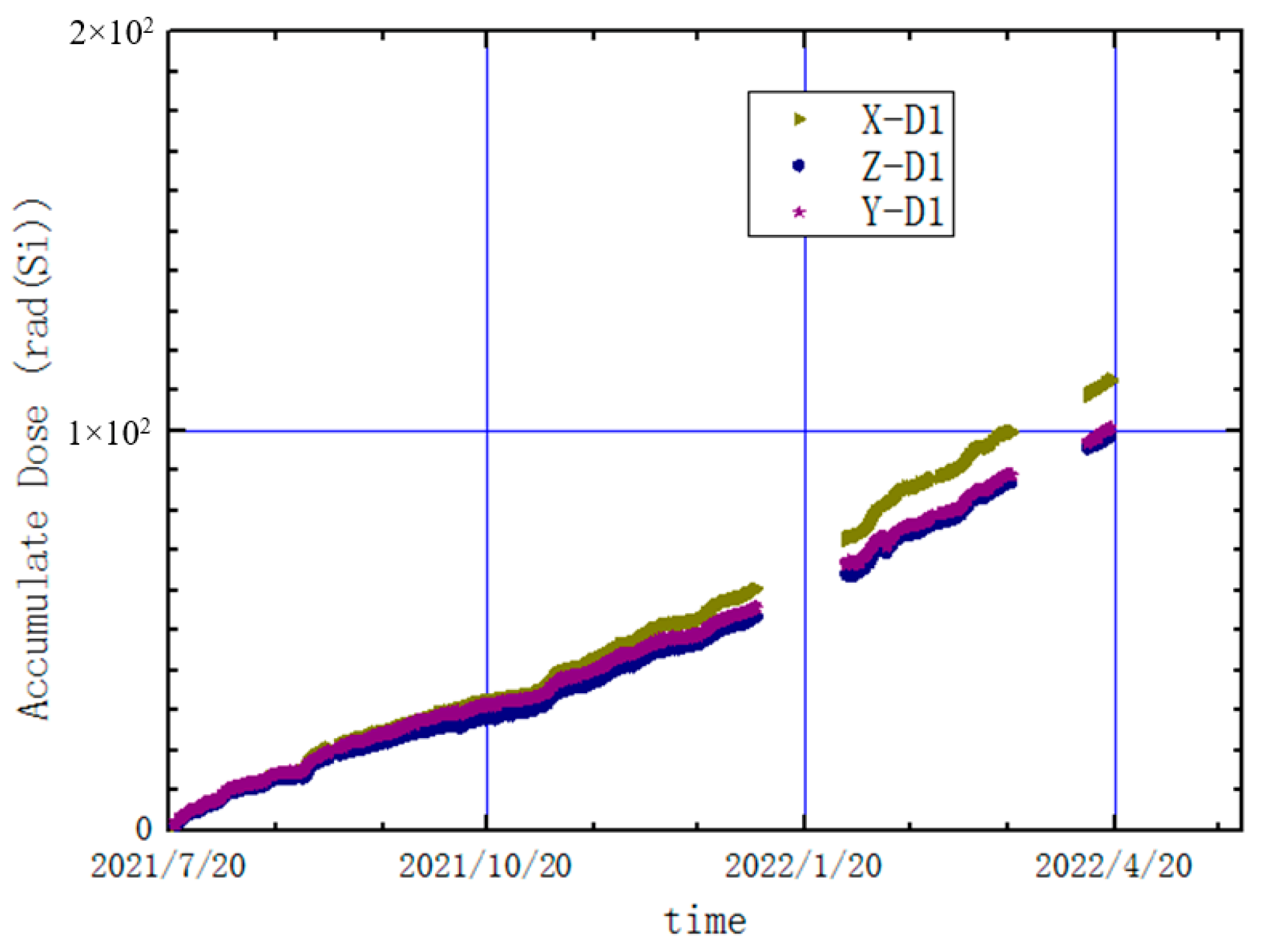
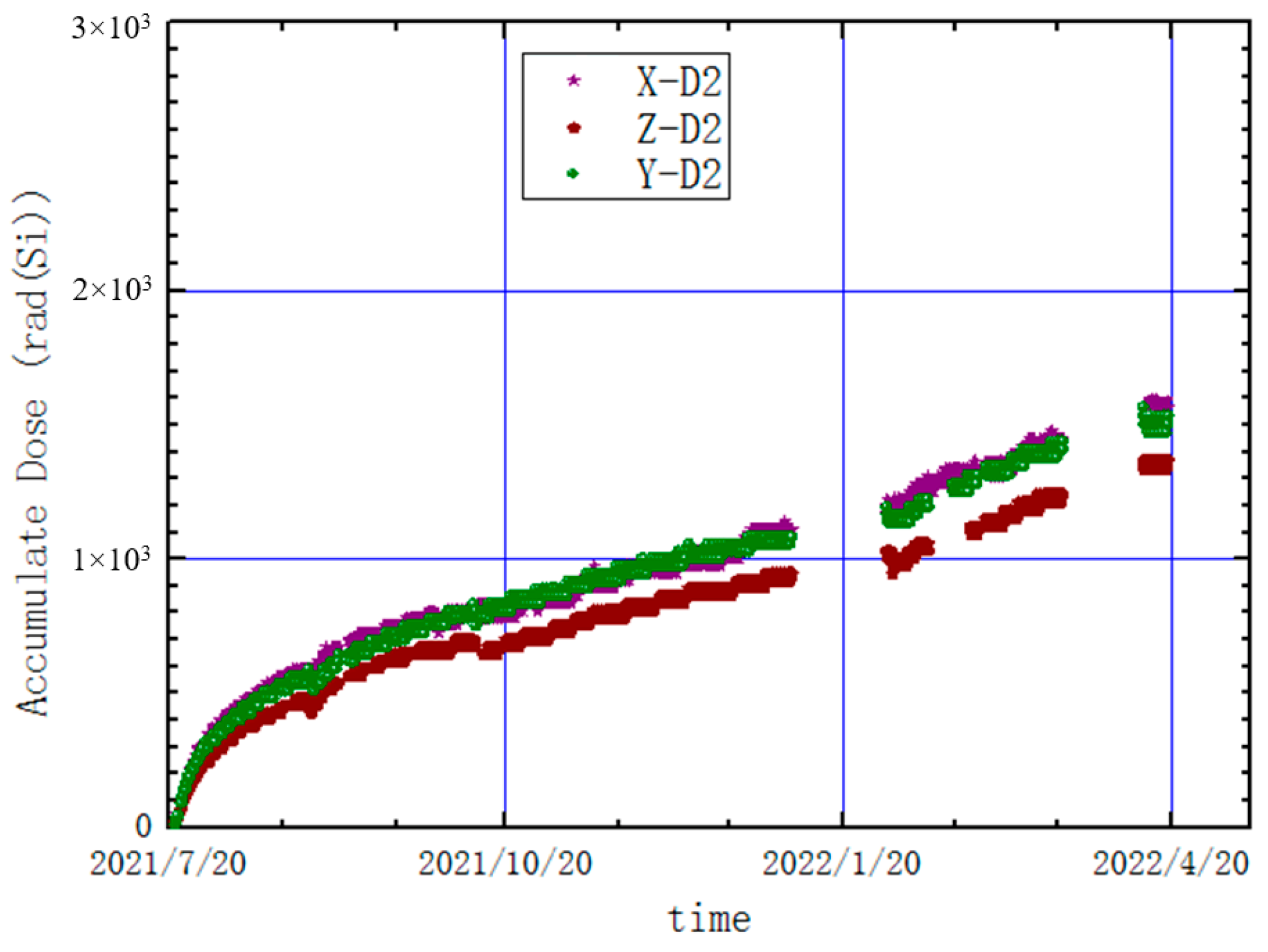
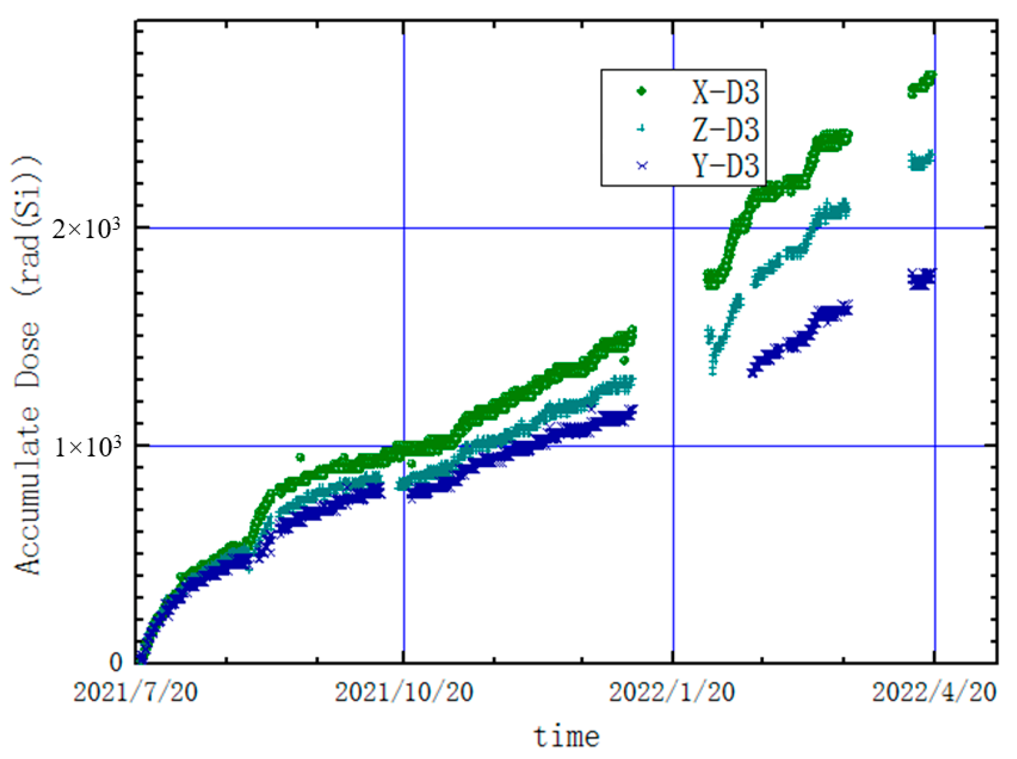
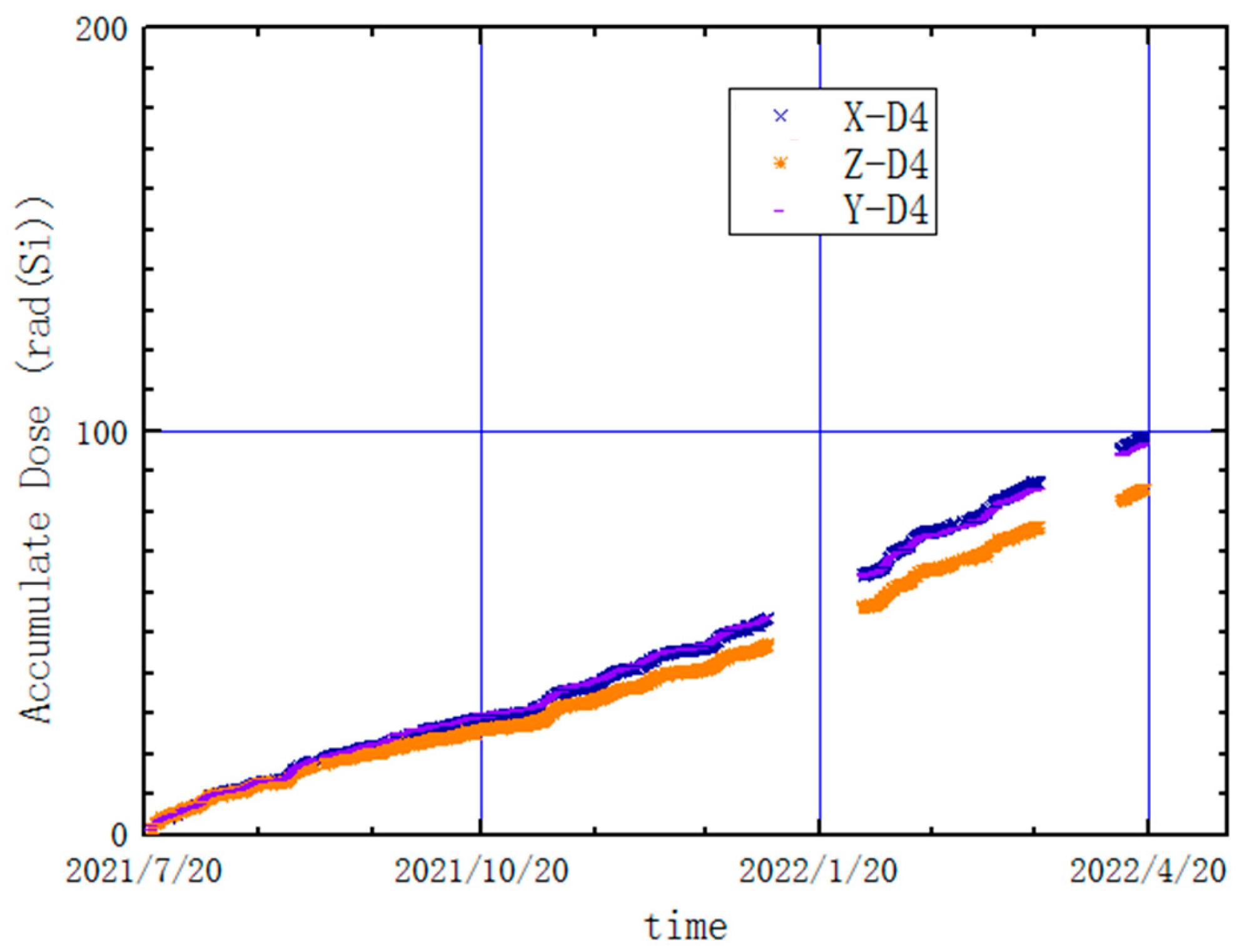
The gate voltage of the PMOS sensor changes with the change in ambient temperature, which affects the accuracy of detection data. Therefore, we should eliminate the change factor of the sensor gate voltage affected by a temperature change. All detectors have undergone a temperature cycling test on ground. We obtained the relationship between the sensor gate voltage and the temperature change without radiation. In this way, we can remove the influence of the PMOS sensor temperature on the space irradiation dose. Next, the change in gate voltage caused by the PMOS sensor only affected by space radiation at each time is calculated, and the cumulative dose of space radiation is finally obtained from the calibration curve. This makes the detection data more accurate. Figure 8, Figure 9, Figure 10, Figure 11 and Figure 12 are the results of detection data obtained after temperature correction.
We analyzed the data from the power-up of the detector to April 2022. There were two gaps around 20 January and the end of March 2022, which are data missing. From the current detection results, the cumulative dose in the X direction is the largest among the three satellite directions. The maximum cumulative dose detected has reached 2.7 k rad(Si). The different doses in the X, Y and Z directions indicate that the particle radiation level of the satellite in different directions is not the same.
In the aforementioned content, we have already mentioned that the front panels of the five sensors are Al structures with five kinds of thicknesses. The thickness is 3.5 mm, 1 mm, 0 mm, 6 mm and 2.5 mm, which corresponds to D1 to D5, respectively. Moreover, considering the shielding effect in other directions of the structure of the payload and the equivalent 1 mm thickness of the satellite skin, the actual equivalent Al shielding thickness of each sensor is shown in Table 5.
Under different shielding thicknesses, the total radiation dose received has a certain difference. From Figure 7 and Figure 11, we can find that the total dose detected by D2 and D3 is far greater than the total dose detected by D1, D4 and D5, which is mainly caused by the difference in shielding thickness. As of 19 April 2022, the cumulative dose measured under different shielding thicknesses in each direction is shown in Table 6. It can be seen from the table that when the shielding thickness increases from 1.8 mm to 2.8 mm, the cumulative dose decreases by about 40%. When the shielding thickness is more than 6 mm, the cumulative dose does not change significantly.
In 2004, scientists had conducted some analysis and research on the relationship between cumulative dose and shielding thickness [12]. We found that when the thickness of Al is greater than about 6.5 mm, the total dose level does not change obviously with the increase in the shielding thickness. Therefore, the five shielding thicknesses designed meet the research requirement. There are two types of shielding thickness less than 6.5 mm, two types of shielding thickness greater than 6.5 mm and one type of shielding thickness equal to 6.5 mm.
The daily average dose under different shielding thicknesses in each direction was further calculated from the above table, and the results are shown in Table 7. The daily average dose decreases exponentially with the increase in the shielding thickness. When the shielding thickness is greater than 6.5 mm, the daily average dose does not change significantly with the increase in the shielding thickness and basically remains at the level of 0.4 rad(Si)·d−1.
From these analysis data, it can be found that when the shielding thickness is less than 6 mm, the radiation dose level is closely related to the shielding thickness. As the cumulative dose increases, the difference becomes increasingly obvious. The shell structure thickness of the satellite load is generally less than 6 mm. Therefore, the detection results of the radiation dose detector show that the radiation protection design of the payload is necessary and that the method of carrying out the protection design more reasonably is important.
6. Conclusions
The radiation dose detector onboard the FY-4B satellite has adopted a new detection technology. Each detector includes 5 dose detection points, and 3 dose detectors have a total of 15 dose detection points. Five kinds of shielding thickness are set for five dose-monitoring points in each detector. In this way, the real total dose in-orbit detection data under different shielding thicknesses can be obtained. More accurate detection data can provide a more accurate data basis for engineering applications and can more effectively guide the reasonable layout of the internal components of the satellite.
The radiation dose detector carried on the FY-4B satellite has the characteristics of small volume, low power consumption and high integration. Each dose detector is equipped with several dose-monitoring points, which can realize the combined detection of a large range and high precision. The FY-4B satellite was successfully launched in June 2021. Since its startup, the radiation dose detector has been working normally and the preliminary detection results are good. From the power-up of the detector to April 2022, the maximum dose has reached 2.7 × 10³ rad(Si). Through the concrete analysis of five kinds of shielding thickness, the accurate equivalent shielding thickness can be obtained, which has good correspondence with in-orbit detection results. In addition, we conducted a preliminary analysis of the relationship between total dose and shielding thickness. In addition, the relationship between daily average dose and shielding thickness was further analyzed. These studies have certain application value for radiation protection design of the payload.
When the in-orbit cumulative dose is small, the detection data have some errors. With the increase in the cumulative dose, the detection data become increasingly accurate. After accumulating detection data for a long time in the later stage, we believe there will be more meaningful results that can promote the development of space total dose detection technology and promote the applied research of the space environment.
Author Contributions
Conceptualization, Y.S. and B.Z.; Methodology, S.Z. and G.S.; Software, X.Z. (Xin Zhang); Validation, H.Z.; Formal Analysis, T.J.; Investigation, B.Z.; Resources, X.Z. (Xiaoxin Zhang); Data Curation, X.Z. (Xiaoxin Zhang), X.Z. (Xianguo Zhang), C.H., J.L. and W.Z.; Writing—Original Draft Preparation, Y.S. and B.Z.; Writing—Review & Editing, Y.S., X.Z. (Xiaoxin Zhang), G.S., T.J., S.Z., X.Z. (Xianguo Zhang), C.H., J.L., W.Z., X.Z. (Xin Zhang) and H.Z.; Supervision, T.J. and X.Z. (Xianguo Zhang); ProjectAdministration, G.S. All authors have read and agreed to the published version of the manuscript.
Funding
This work was supported by the National Natural Science Foundation of China (41931073) and the National Key R&D Program of China (2021YFA0718600).
Data Availability Statement
No new data created or analyzed in this study. Data sharing is not applicable to this article.
Acknowledgments
We thank the following facility and personnel for supporting the calibration of dose detectors: Xinjiang Technical Institute of Physics & Chemistry, the Chinese Academy of Sciences, China. We thank Jing Sun provides service of calibration.
Conflicts of Interest
The authors declare no conflict of interest.
References
- August, L.S.; Circle, R.R. Advantages of using a PMOS FET dosimeter in high-dose radiation effects testing. IEEE Trans. Nucl. Sci. 1984, 31, 1113–1115. [Google Scholar] [CrossRef]
- Kelleher, A.; Lane, W.; Leonard, A. A design solution to increasing the sensitivity of PMOS dosimeters: The stacked RADFET approach. IEEE Trans. Nucl. Sci. 1995, 42, 48–51. [Google Scholar] [CrossRef]
- Schwank, J.R.; Roeske, S.B.; Beutler, D.E.; Moreno, D.J.; Shaneyfelt, M.R. A dose rate independent PMOS dosimeter for space applications. IEEE Trans. Nucl. Sci. 1996, 43, 2671–2678. [Google Scholar] [CrossRef]
- Dyer, C.S.; Watson, C.J.; Peerless, C.I.; Sims, A.J.; Barth, J. Measurements of the radiation environment from CREDO-11 on STRV&APEX. IEEE Trans. Nucl. Sci. 1996, 43, 2751–2757. [Google Scholar] [CrossRef]
- Bühler, P.; Desorgher, L.; Zehnder, A.; Daly, E.; Adams, L. Observations of the low earth orbit radiation environment from MIR. Radiat. Meas. 1996, 26, 917–921. [Google Scholar] [CrossRef] [PubMed] [Green Version]
- Bogorad, A.; Bowman, C.; Dennis, A.; Beck, J.; Lang, D.; Herschitz, R.; Buehler, M.; Blaes, B.; Martin, D. Integrated environmental monitoring system for spacecraft. IEEE Trans. Nucl. Sci. 1995, 42, 2051–2057. [Google Scholar] [CrossRef]
- MacKay, G.F.; Thomson, I.; Ng, A.; Sultan, N. Applications of MOSFET dosimeters on MIR and BION satellites. IEEE Trans. Nucl. Sci. 1997, 44, 2048–2051. [Google Scholar] [CrossRef]
- Xiaochao, Y.; Shijin, W.; Yue, W.; Wei, Z. Observation and research of space particle radiation dose on sun-synchronous orbit. J. Astronaut. 2008, 29, 357–361. [Google Scholar]
- Sun, J.; Guo, Q.; Zhang, J.; Ren, D.Y.; Lu, W.; Yu, X.F.; Wen, L.; Wang, G.l.; Zhang, Y.H. Influence of dose rate on radiation response of PMOSFET dosimeter. Microelectronics 2009, 39, 128–131. [Google Scholar]
- Chen, C.L. Simulation and Studying of PMOS Radiation Sensors. Master’s Thesis, Jiangnan University, Wuxi, China, March 2011. [Google Scholar]
- Sun, Y.; Zhang, B.Q.; Zhang, X.; Zhang, X.; Zhang, S.; Shen, G.; Chang, Z.; Wang, C.; Sun, Y.; Zong, W.; et al. Design spaceborne of radiation dosimeter in depth. Chin. J. Space Sci. 2021, 41, 793–799. [Google Scholar] [CrossRef]
- Cai, Z.B. Space Radiation Dose Analysis of Dual-Satellite Exploration Satellite; Special Committee of Space Exploration of China Society of Space Research: Beihai, China, 2003. [Google Scholar]
Figure 1.
The composition block diagram of the radiation dose detector.

Figure 2.
Received irradiation dose and corresponding voltage output of PMOS sensors. (a) Received irradiation dose and corresponding voltage output of the 100 nm PMOS sensor. (b) Received irradiation dose and corresponding voltage output of the 400 nm PMOS sensor.
Figure 2.
Received irradiation dose and corresponding voltage output of PMOS sensors. (a) Received irradiation dose and corresponding voltage output of the 100 nm PMOS sensor. (b) Received irradiation dose and corresponding voltage output of the 400 nm PMOS sensor.

Figure 3.
Electronic principle diagram of the radiation dose detector.

Figure 4.
The three-dimensional picture of the dose detector.

Figure 5.
The photograph of the radiation dose detector.

Figure 6.
The scheme of the dose calibration test.

Figure 7.
A sketch of the satellite position with reference to Earth and the detection direction of the dose detector.
Figure 7.
A sketch of the satellite position with reference to Earth and the detection direction of the dose detector.

Figure 8.
Cumulative dose results of the three dose detectors at monitoring point D1.

Figure 9.
Cumulative dose results of the three dose detectors at monitoring point D2.

Figure 10.
Cumulative dose results of the three dose detectors at monitoring point D3.

Figure 11.
Cumulative dose results of the three dose detectors at monitoring point D4.

Figure 12.
Cumulative dose results of the three dose detectors at monitoring point D5.


Table 1.
The main technical indexes of the radiation dose detector.
| Items | Dose Detection Points | Index (rad(Si)) |
|---|---|---|
| Detection range | D1 | 2.0 × 10⁴ |
| D2 | 4.0 × 10⁵ | |
| D3 | 2.0 × 10⁶ | |
| D4 | 8.0 × 10³ | |
| D5 | 4.0 × 10⁴ | |
| Detection accuracy | 15% | |
Table 2.
The main engineering indexes of the radiation dose detector.
| Index Items | Electric Control Unit | Dose Detector |
|---|---|---|
| Body size | 140 mm × 85 mm × 60 mm | 137 mm × 48 mm × 106 mm |
| Weight | 0.8 ± 0.03 kg | 0.8 ± 0.03 kg |
| Power consumption | <1.4 W | <0.65 W |
| Working temperature | −15 °C~+45 °C | −15 °C~+45 °C |
Table 3.
The conversion parameters’ value for the 400 nm and 100 nm sensors.
| Sensors | A1 | A2 | A3 |
|---|---|---|---|
| 100 nm | 214,086.49 | 28,510.88 | −1033.28 |
| 400 nm | 990.14 | 2067.62 | −30.28 |
Table 4.
Calibration results of the dose detector.
| Detection Points | Design Range (rad(Si)) | Calibration Results (rad(Si)) | Sensitivity (rad(Si)) | Accuracy |
|---|---|---|---|---|
| D1 | 2.0 × 10⁴ | 2.2 × 10⁴ | 1.42 | ≤7.2% |
| D2 | 4.0 × 10⁵ | 4.1 × 10⁵ | 16.2 | ≤10.2% |
| D3 | 2.0 × 10⁶ | 2.0 × 10⁶ | 114.9 | ≤10.2% |
| D4 | 8.0 × 10³ | 9.1 × 10³ | 1.0 | ≤7.2% |
| D5 | 4.0 × 10⁴ | 4.1 × 10⁴ | 4.0 | ≤7.2% |
Table 5.
Equivalent shielding thickness corresponding to each sensor.
| Detection Points | Types | Shielding Thicknesses |
|---|---|---|
| D1 | 400 nm | 6.5 mm |
| D2 | 100 nm | 2.8 mm |
| D3 | 100 nm | 1.8 mm |
| D4 | 400 nm | 8.6 mm |
| D5 | 400 nm | 6.7 mm |
Table 6.
The cumulative dose measured under different shielding thicknesses in each direction.
| Direction | Cumulative Dose under Each Equivalent Al Shielding Thickness (rad(Si)) | ||||
|---|---|---|---|---|---|
| 1.8 mm | 2.8 mm | 6.7 mm | 6.5 mm | 8.6 mm | |
| X | 2704.2 | 1563.1 | 101.1 | 113.0 | 98.2 |
| Y | 1791.6 | 1335.0 | 88.3 | 100.5 | 96.6 |
| Z | 2111.2 | 1224.3 | 93.7 | 98.8 | 85.5 |
Table 7.
The daily average dose under different shielding thicknesses in each direction.
| Direction | Daily Average Dose under Each Equivalent Al Shielding Thickness (rad(Si)) | ||||
|---|---|---|---|---|---|
| 1.8 mm | 2.8 mm | 6.7 mm | 6.5 mm | 8.6 mm | |
| X | 9.91 | 5.73 | 0.37 | 0.41 | 0.36 |
| Y | 6.56 | 4.89 | 0.32 | 0.37 | 0.35 |
| Z | 7.73 | 4.48 | 0.34 | 0.36 | 0.31 |
Disclaimer/Publisher’s Note: The statements, opinions and data contained in all publications are solely those of the individual author(s) and contributor(s) and not of MDPI and/or the editor(s). MDPI and/or the editor(s) disclaim responsibility for any injury to people or property resulting from any ideas, methods, instructions or products referred to in the content. |
© 2023 by the authors. Licensee MDPI, Basel, Switzerland. This article is an open access article distributed under the terms and conditions of the Creative Commons Attribution (CC BY) license (https://creativecommons.org/licenses/by/4.0/).
Share and Cite
MDPI and ACS Style
Sun, Y.; Zhang, B.; Zhang, X.; Shen, G.; Jing, T.; Zhang, S.; Zhang, X.; Huang, C.; Li, J.; Zong, W.; et al. Radiation Dose Detection on FY-4B Satellite. Aerospace 2023, 10, 325. https://doi.org/10.3390/aerospace10040325
AMA Style
Sun Y, Zhang B, Zhang X, Shen G, Jing T, Zhang S, Zhang X, Huang C, Li J, Zong W, et al. Radiation Dose Detection on FY-4B Satellite. Aerospace. 2023; 10(4):325. https://doi.org/10.3390/aerospace10040325
Chicago/Turabian StyleSun, Ying, Binquan Zhang, Xiaoxin Zhang, Guohong Shen, Tao Jing, Shenyi Zhang, Xianguo Zhang, Cong Huang, Jiawei Li, Weiguo Zong, and et al. 2023. "Radiation Dose Detection on FY-4B Satellite" Aerospace 10, no. 4: 325. https://doi.org/10.3390/aerospace10040325
Note that from the first issue of 2016, this journal uses article numbers instead of page numbers. See further details here.