Article

Characteristics Mode Analysis-Inspired Compact UWB Antenna with WLAN and X-Band Notch Features for Wireless Applications

1
Department of Electronics and Communication Engineering, Manipal Institute of Technology, Manipal Academy of Higher Education, Manipal 576104, India
2
Department of Information and Communication Technology, Manipal Institute of Technology, Manipal Academy of Higher Education, Manipal 576104, India
3
Discipline of Electrical, Electronic and Computer Engineering, University of KwaZulu-Natal, Durban 4041, South Africa
4
Department of Electronics and Communication Engineering, Sri Sivasubramaniya Nadar College of Engineering, Chennai 603110, India
*
Author to whom correspondence should be addressed.
J. Sens. Actuator Netw. 2023, 12(3), 37; https://doi.org/10.3390/jsan12030037
Submission received: 10 March 2023 / Revised: 20 April 2023 / Accepted: 20 April 2023 / Published: 23 April 2023
(This article belongs to the Topic Electronic Communications, IOT and Big Data)

Abstract

:
A compact circular structured monopole antenna for ultrawideband (UWB) and UWB dual-band notch applications is designed and fabricated on an FR4 substrate. The UWB antenna has a hybrid configuration of the circle and three ellipses as the radiating plane and less than a quarter-lowered ground plane. The overall dimensions of the projected antennas are 16 × 11 × 1.6 mm3, having a −10 dB impedance bandwidth of 113% (3.7–13.3 GHz). Further, two frequency band notches were created using two inverted U-shaped slots on the radiator. These slots notch the frequency band from 5–5.6 GHz and 7.3–8.3 GHz, covering IEEE 802.11, Wi-Fi, WLAN, and the entire X-band satellite communication. A comprehensive frequency and time domain analysis is performed to validate the projected antenna design’s effectiveness. In addition, a circuit model of the projected antenna design is built, and its performance is evaluated. Furthermore, unlike the traditional technique, which uses the simulated surface current distribution to verify functioning, characteristic mode analysis (CMA) is used to provide deeper insight into distinct modes on the antenna.

1. Introduction

Ultrawideband (UWB) communication systems have emerged as the most feasible solution for short-range, high-speed indoor data communications since the Federal Communication Commission (FCC) released the bandwidth 3.1–10.6 GHz. Following the FCC approval in 2002 for commercial use, UWB communication systems have grown popular among researchers and the wireless sectors [1]. As a result, a critical component of UWB communication systems, UWB antennas, has piqued numerous researchers’ curiosity. The transmission and reception of signals in the UWB system use short electromagnetic pulses. The system’s performance is principally governed by the characteristics of the radiators, which must meet rigorous frequency and time domain criteria across the entire working spectrum [2]. These specifications comprise a non-dispersive phase center, consistent radiation characteristics, and an impedance bandwidth without the stimulation of higher-order modes [3]. The monopole patch antenna arrangement has a small size, low cost, and broader impedance bandwidth, which is well-anticipated for UWB wireless applications [4]. So far, various types of monopole antenna geometries have been developed to cover the whole frequency range of UWB, comprising various types of radiating structures, engraving ground planes, embedding slits, slots, stubs on radiating, and ground planes as parasitic elements, as well as metamaterial loading [5,6,7,8,9,10,11]. The progress of wireless communication systems and the growing interest in wireless small-hand devices have increased the demand for operational frequency bands. This scenario has led to the crowded radio spectrum, and the regular frequency bands have begun to overlap. Even though the large frequency bandwidth of UWB systems offers several benefits, it creates interference with conventional wireless communication systems operating at different narrowband frequencies, such as the worldwide interoperability for microwave access (WiMAX) (3.3–3.7 GHz), C-band systems (3.7–4.2 GHz), the IEEE 802.1a standard-based wireless local network (WLAN) (5.15–5.825 GHz), and X-band satellite communication (7.25–7.745 GHz and 7.9–8.395 GHz) [12]. Therefore, compact large impedance bandwidth antennas having band-reject properties are needed for UWB applications. Different UWB antenna design techniques are available, such as dielectric resonators (DRAs) [13,14] and microstrip patch antennas (MPA)s. The distinctive features of both types of antennas are determined by their dielectric characteristics. Despite the fact that DRAs appear to be more efficient than MPAs in several aspects, MPAs have benefits in mechanical processing, gain, and stability over DRAs [15].
Conventional approaches for band rejection features are primarily focused on using a half- or quarter-wavelength filter configuration in an antenna’s design. The literature reveals many ideas for achieving single- and multi-band-notched features in UWB antennas [16,17,18], for example, an L-shaped slit on a radiating plane [19]; metamaterial loadings such as a split-ring resonator (SRR) and a complementary split-ring resonator (CSRR; the structure is not limited to the circle) [20,21]; a bent slit engraved on a radiating plane [22], where different structures such as L, Z, and G are etched on a radiating or ground plane [23,24] and are connected via the method described in [25]. In [26], a half-circle was embedded in a combination of two rectangular patches to achieve the UWB spectrum. The UWB dual-band notch was shown by the authors of [10] at 3.5 and 5.5 GHz. By placing J and inverted pi form slots onto the radiating plane, the WiMAX and WLAN band interference with the UWB was removed. In [24], a Z-shaped slot was engraved on the ground plane to achieve a frequency notching at the WLAN band. Reference [20] used an elliptical CSRR on a radiating plane to attain frequency notching characteristics at the WiMAX and WLAN bands. Dual-band notching is achieved in [19] by carving two L-shaped grooves on a radiator. The design of a wider impedance bandwidth antenna with compactness is challenging. A majority of the prior works lack notching of the complete existing narrowbands. This paper presents a composite structure of a circular- and ellipse-shaped UWB antenna with a simulated and measured impedance bandwidth of approximately 113% (3.7–13.3 GHz). The proposed design exhibits two frequency band notchings: one at 5–5.6 GHz, covering the WLAN and IEEE 802.11 bands, and one at 7.3–8.3 GHz, covering X-band satellite communication. Incorporating sequences of ellipses onto the circular monopole and the lowered ground plane embedded with an arc at the edges is responsible for extended ultrawide bandwidth. The inverted U-shaped slots on the UWB antenna radiator help attain two-band notch features by evading impedance matching and disturbing the current distribution. The band-notched mechanism has a negligible influence on the radiation characteristics of the projected antenna. Further, the proposed antenna is evaluated by developing its equivalent circuit and characteristic mode analysis (CMA).
The novelty of the proposed work is that there are no intricate structures used to achieve the UWB spectrum and dual-band notching. This simple structure provides an S11 curve below −11 dB for almost the entire impedance bandwidth. The UWB and UWB band notch structures are compact compared to the many antenna designs in the literature, and significantly less work is reported for the complete band rejection of X-band satellite communication. The projected antenna design is also exposed to a thorough time-domain analysis. A good time-domain response signifies the proposed design’s ability to incorporate it into practical applications. The projected antenna’s prototype is fabricated and measured. The simulation and measured results indicate that it has good frequency and time-domain responses. This work is organized as follows: a detailed design analysis of the projected design is depicted in Section 2. Section 3 describes a comprehensive analysis of the design to find the optimal dimensions. The development of a circuit model for the proposed antenna is depicted in Section 4. Section 5 illustrates the CMA of the proposed UWB antenna. Section 6 describes the experimental and simulated findings of the antenna’s design, followed by concluding remarks.

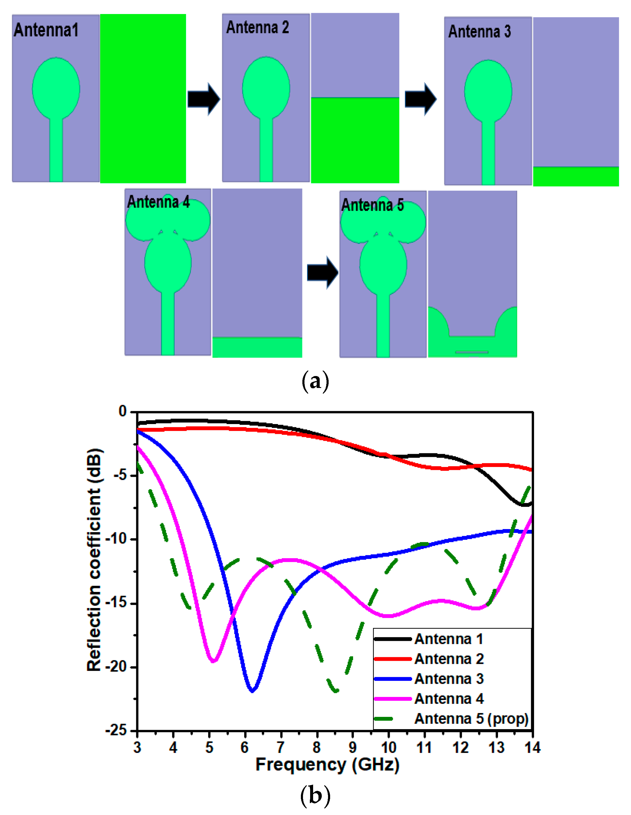
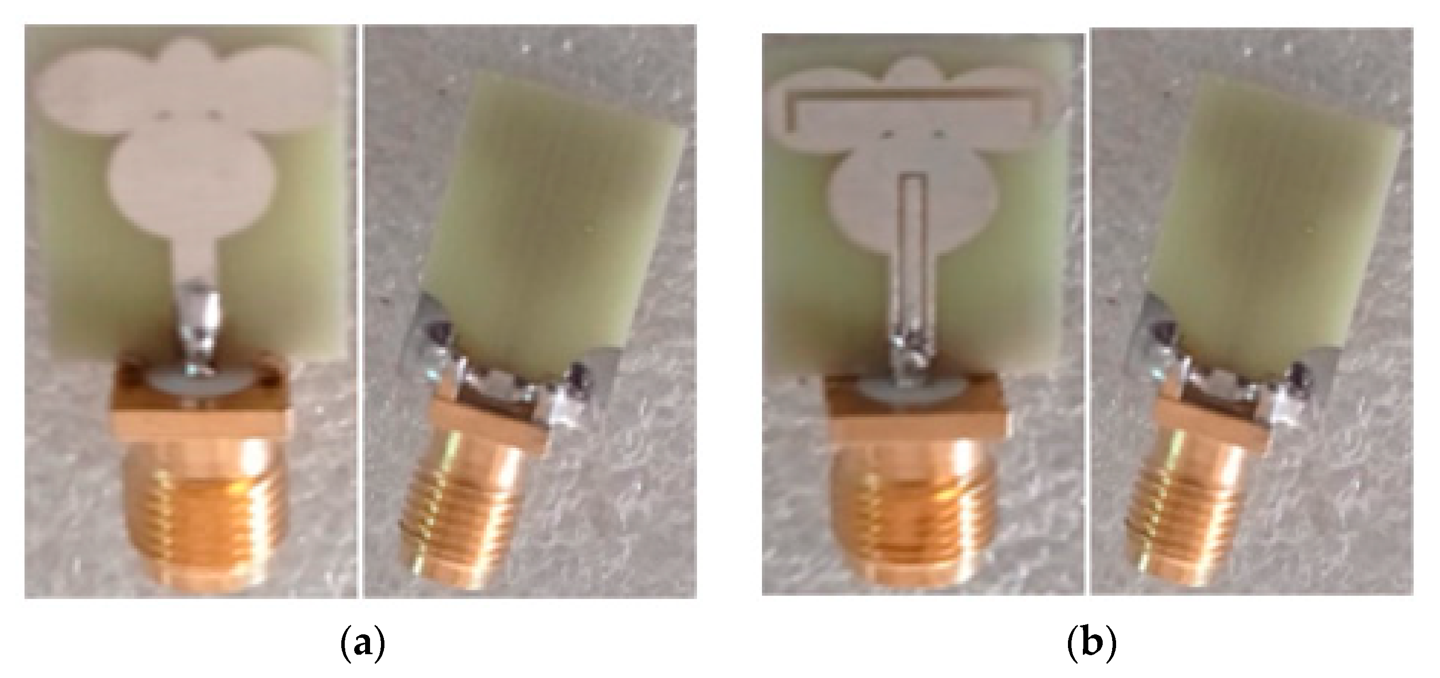
2. Antenna Design Methodology

The proposed configuration of the UWB antenna without band elimination features is fabricated on an FR4 substrate with the dimensions 0.19λ × 0.13λ × 0.01λ, where λ is computed using the lower frequency of 3.7 GHz. An antenna’s step-by-step evolution with its reflection coefficient (S11) is depicted in Figure 1. Antenna 1 is a fundamental circular monopole antenna with a complete ground plane that offers no frequency range below −10 dB in the S11 curve. Antenna 2’s ground plane is reduced to half, resulting in no frequency range below −10 dB in the S11 curve. The further ground plane is lowered to 1.9 mm in antenna 3, which provides an S11 curve ranging from 5.1 to 11.5 GHz. The reduction in the ground plane influences the quality factor, thereby increasing the impedance bandwidth. The impedance bandwidth is further improved in antenna 4 by modifying the radiating plane. Embedding ellipses with the circle arrangement provides an S11 of 4.3–13.6 GHz. Although antenna 4 provides a UWB spectrum, the ground plane of the antenna structure is further analyzed for a stable and broader S11 curve, especially at the lower frequency. Finally, in antenna 5, arc shapes are embedded onto the edges of the ground plane. This configuration exhibits an impedance bandwidth ranging from 3.7 to 13.3 GHz, well below −11 dB.
The circular monopole of antenna 1 is designed with a substrate thickness (h) of 1.6 mm, resonant frequency ( f r ) of 13 GHz, and dielectric constant ( ε r ) of 4.4. The design equations used for determining the patch dimensions are as described in Equations (1)–(3) [27].
The radius (r) of the circular patch is determined by:
  r = F 1 + 2 h π ε r F   ln π F 2 h + 1.7726 ,
where F is given by
F = 8.791 × 10 9 f r ε r .
The effective radius results from the fringing field spreading from the patch border to the ground plane. The fringing field around the circular patch may increase the radius of the circle. Therefore, the effective radius ( r e f f ) is determined as shown below:
  r e f f = 1.8412   c 2 π f r ε r ,
where  c = 3 × 10 11   mm / s .
Parametric analysis is carried out on every design to find an optimum value for the UWB antenna’s geometry. The final dimension for the proposed design is shown in Figure 2. The optimized physical dimension of the proposed UWB configuration is depicted in Table 1.
The frequency band notching is realized by perturbing the radiating plane. This perturbation should not disturb the UWB antenna radiation characteristics over the impedance bandwidth. Consequently, dual-band notch features are attained with the help of an inverted U-shaped slot on the radiator. The inverted U-shaped slot enables a frequency notch ranging from 5 to 5.6 GHz, covering WLAN and IEEE 802.11a/b/j/n/ac/ax standards. Inserting the slots results in an open circuit, avoiding impedance matching and current propagation at the notched frequency. The inverted U-shaped slot radiating-plane configuration helps frequency band elimination from 7.3 to 8.3 GHz, covering the entire X-band satellite communication. The geometric details of the dual-band notch UWB antenna are shown in Figure 3 and Table 2.
The surface current distributions of the UWB and UWB band notches are illustrated in Figure 4 and Figure 5, correspondingly. Regarding the UWB antenna without notch features, it can be noticed in Figure 4a–c that the maximum current concentration is at the feedline at resonance frequencies of 4.5 GHz, 8.5 GHz, and 12.7 GHz. Figure 5a,b shows the current distribution of the UWB antenna with notch characteristics. At the notch frequencies 5.4 GHz and 7.6 GHz, it can be observed that the slots are not allowing the field to propagate into the radiator from the feedline; instead, the maximum current concentration is around the slots. The current distribution plot signifies that the antenna is nonresponsive at the notch frequencies. To calculate the length of the parasitic elements, the following Equations (4) and (5) can be used [11]:
                                                              L p a r a s i t i c   e l e m e n t = λ g 2           ,
where  λ g  is the guided wavelength and is equal to  λ g = λ 0 ε e f f   ; and
L p a r a s i t i c   e l e m e n t = λ 0 2 ε e f f = c 2 f r ε e f f ,
where  ε e f f    is the effective dielectric constant,  f r  is the resonant frequency in GHz, and c is the speed of light.

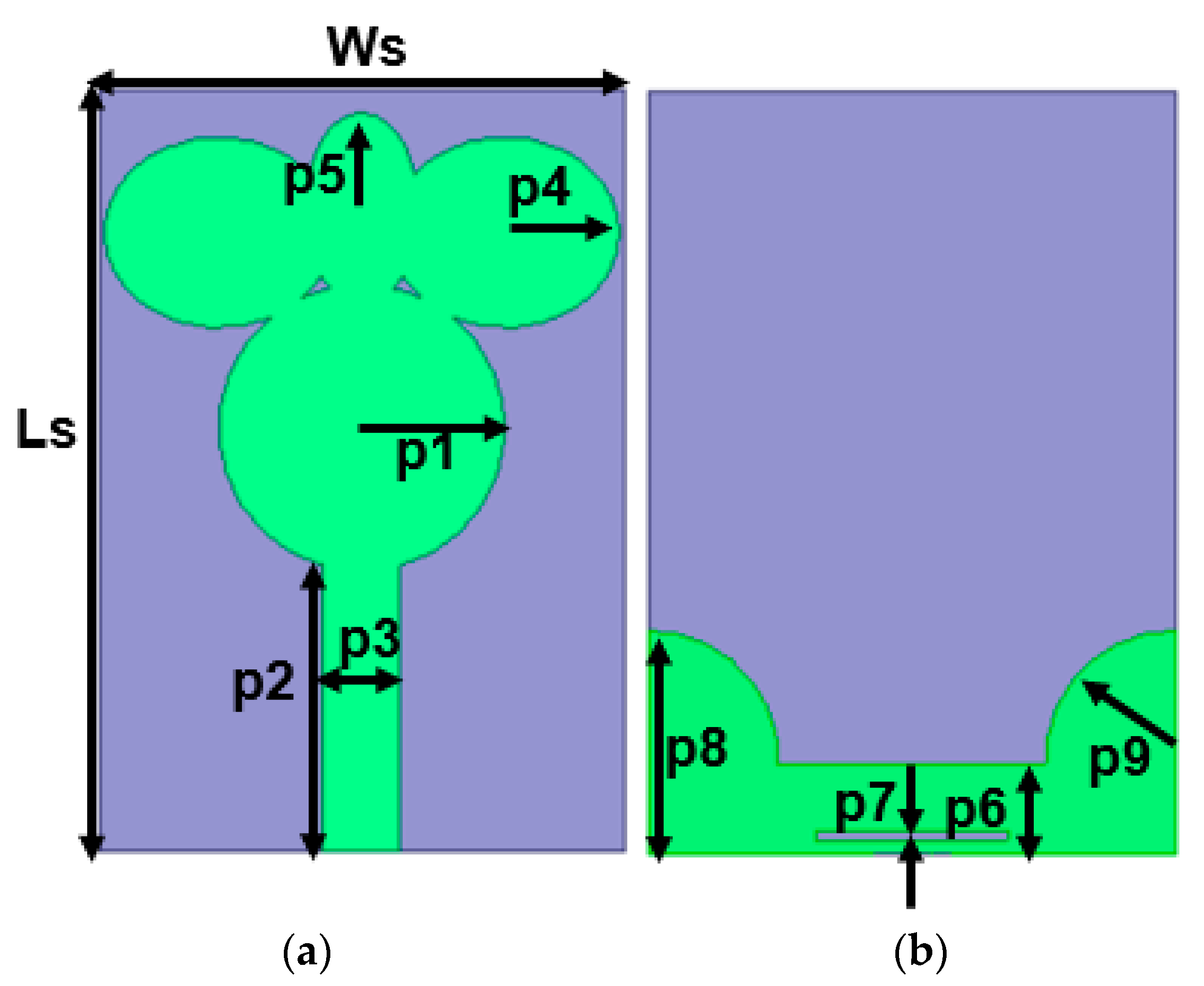
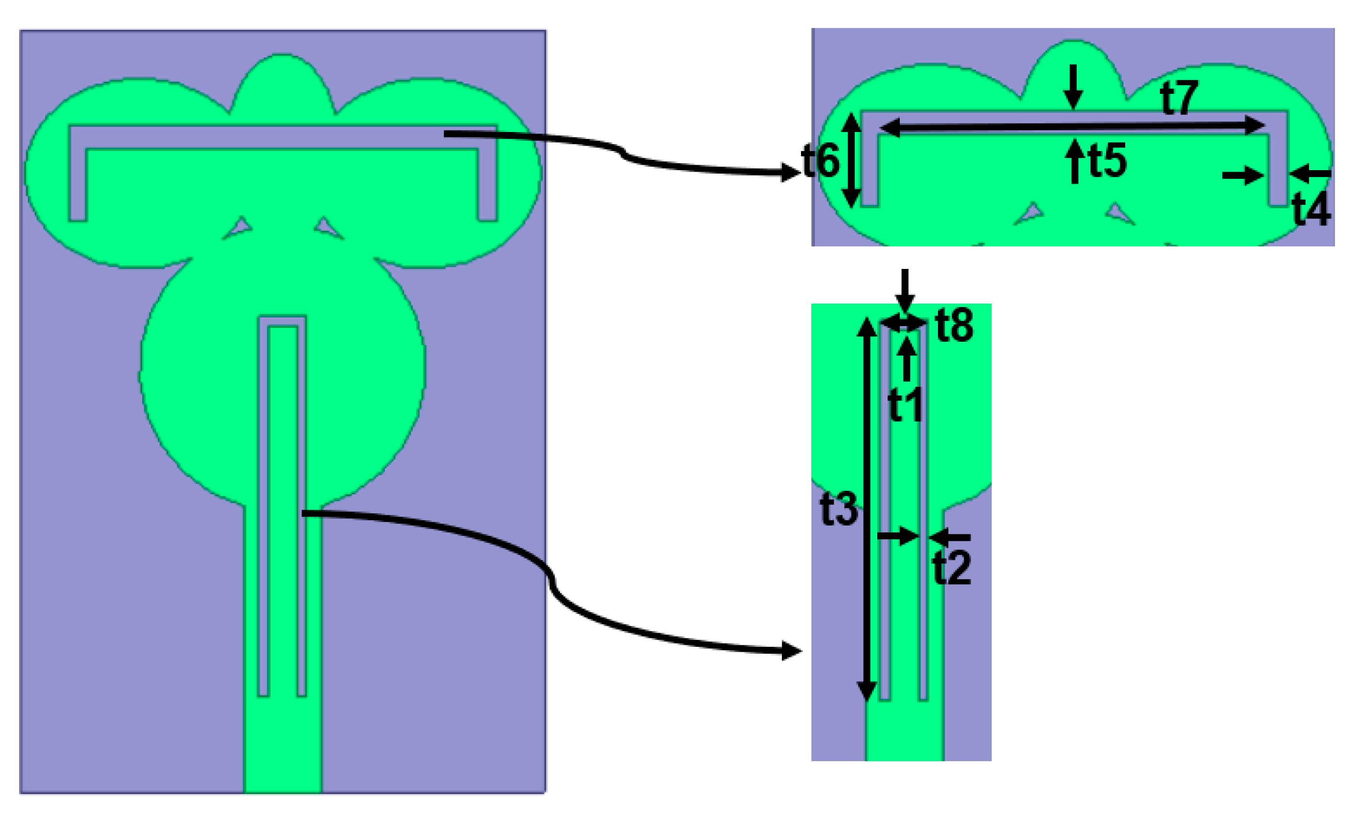
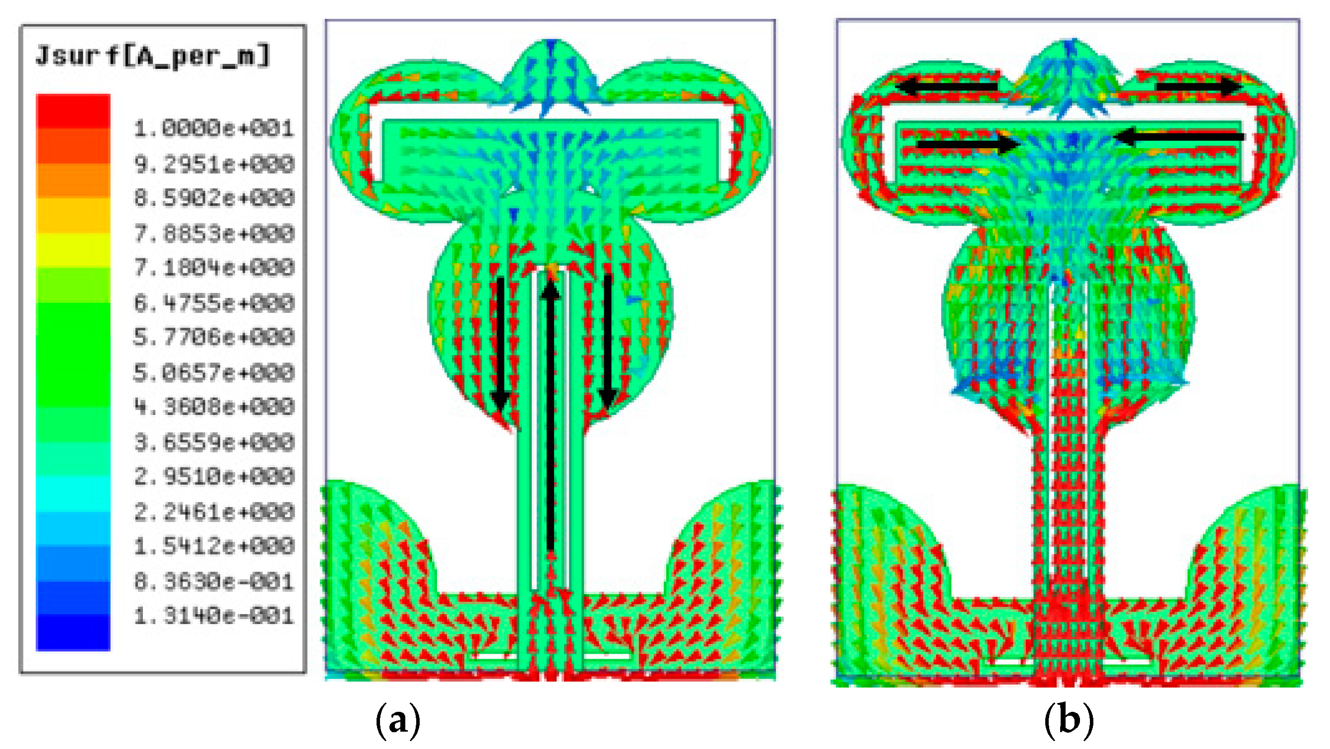
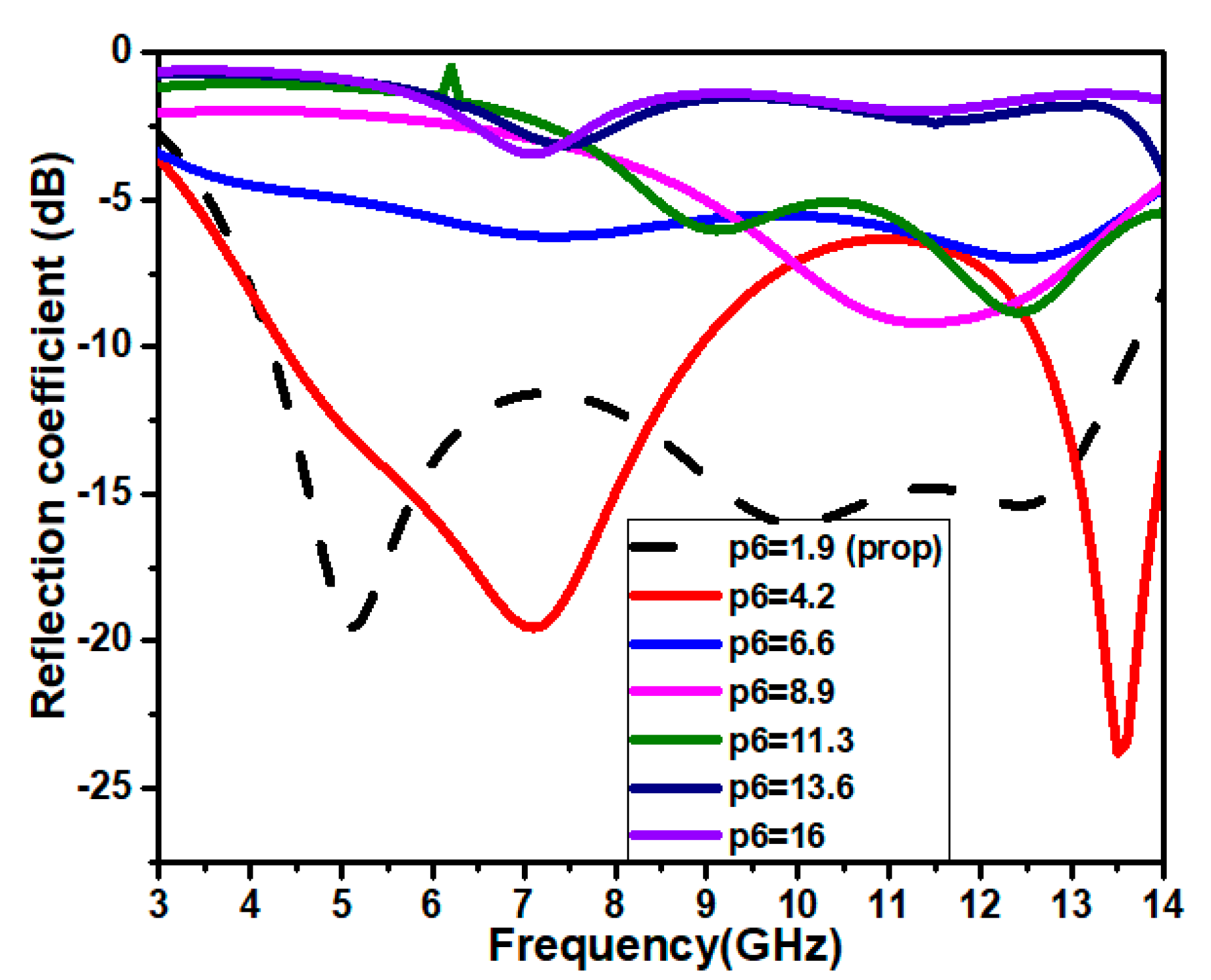
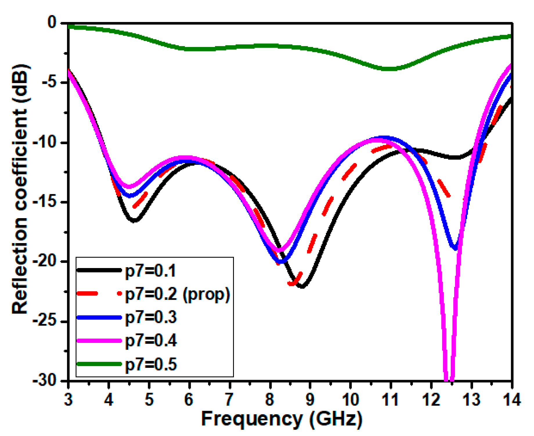
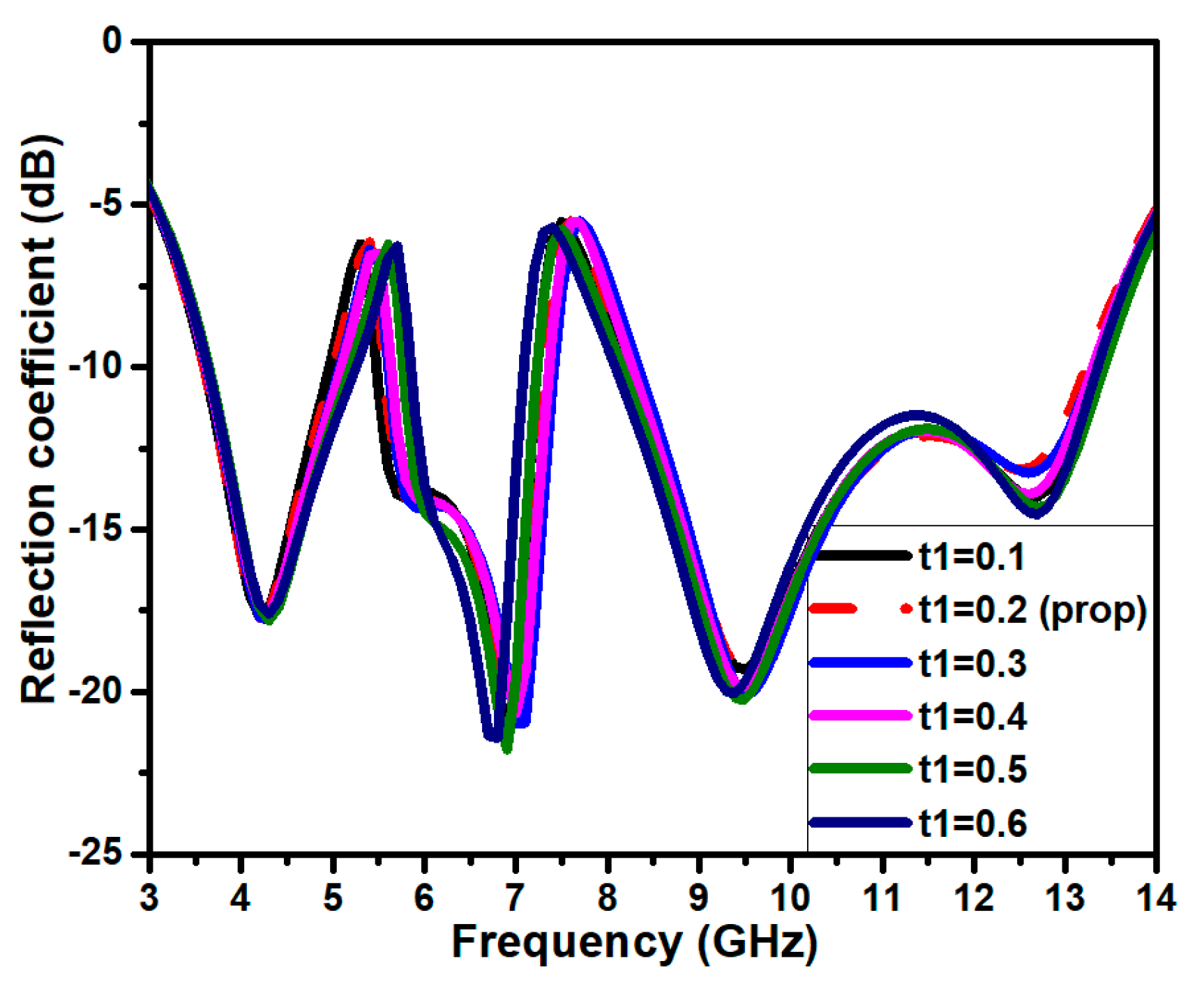
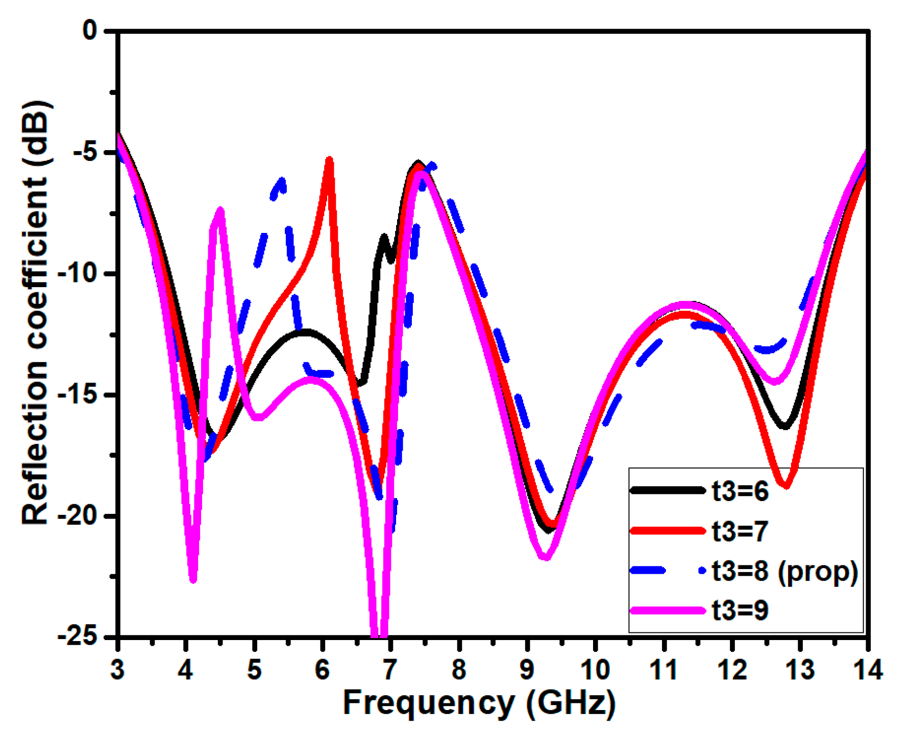
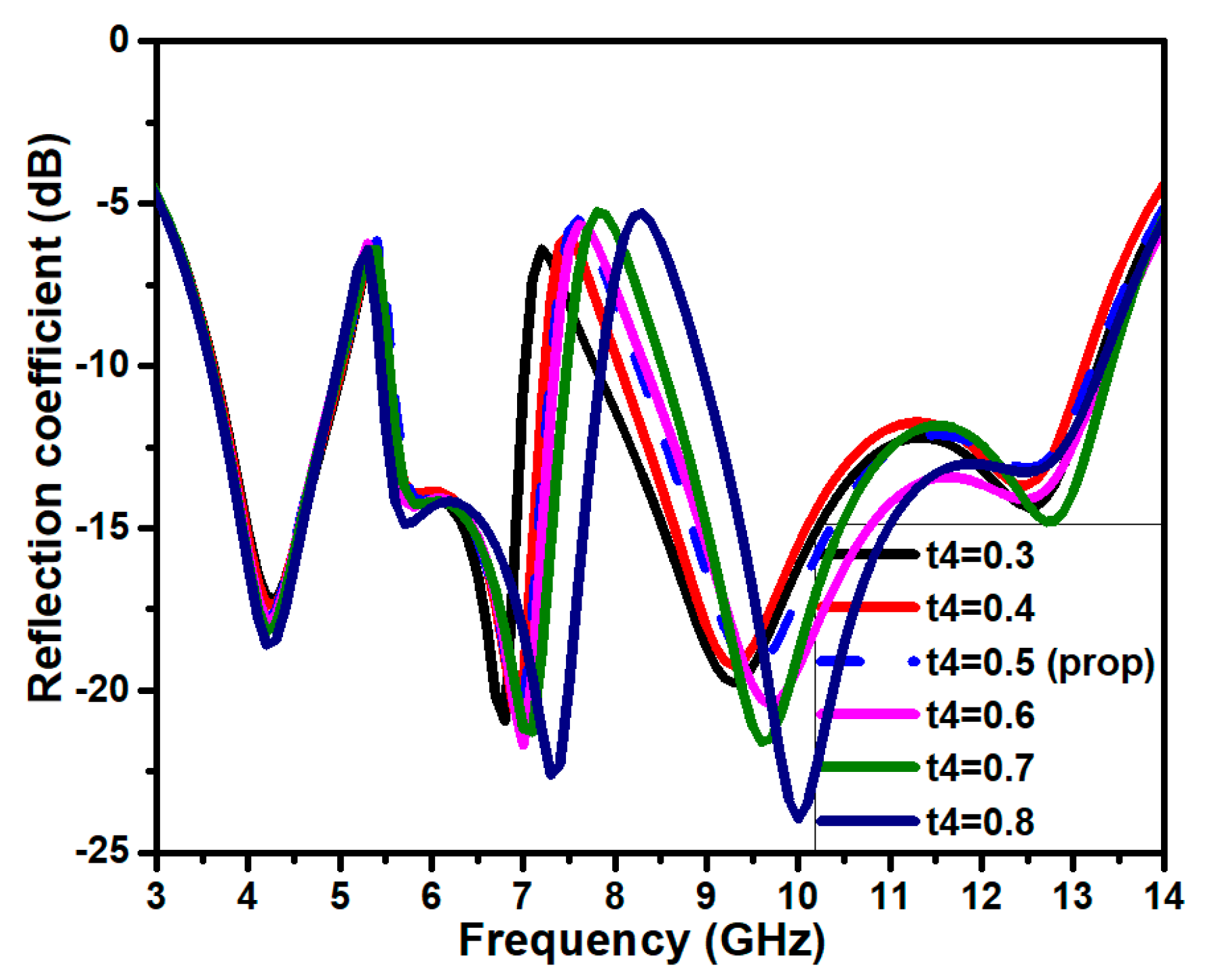
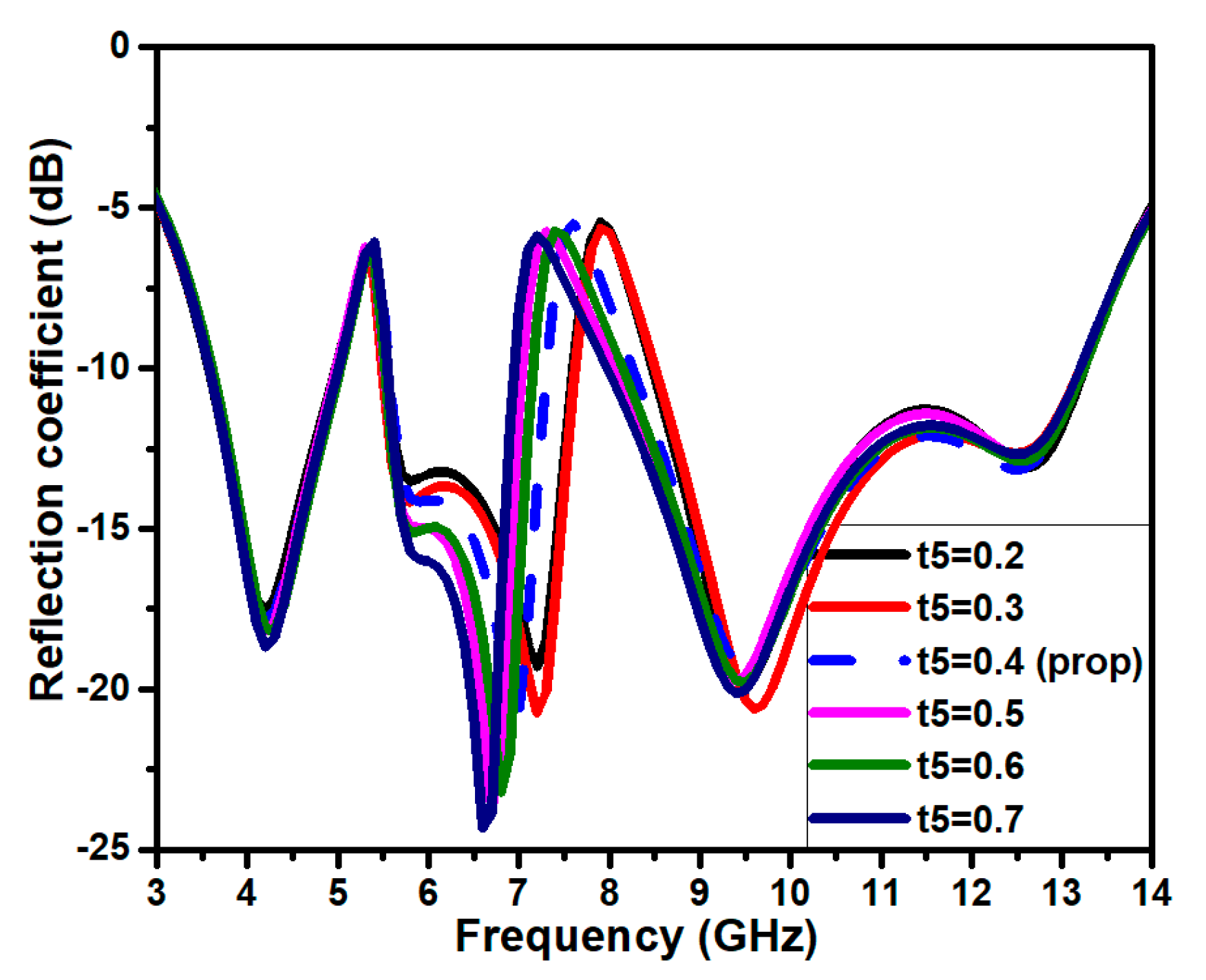
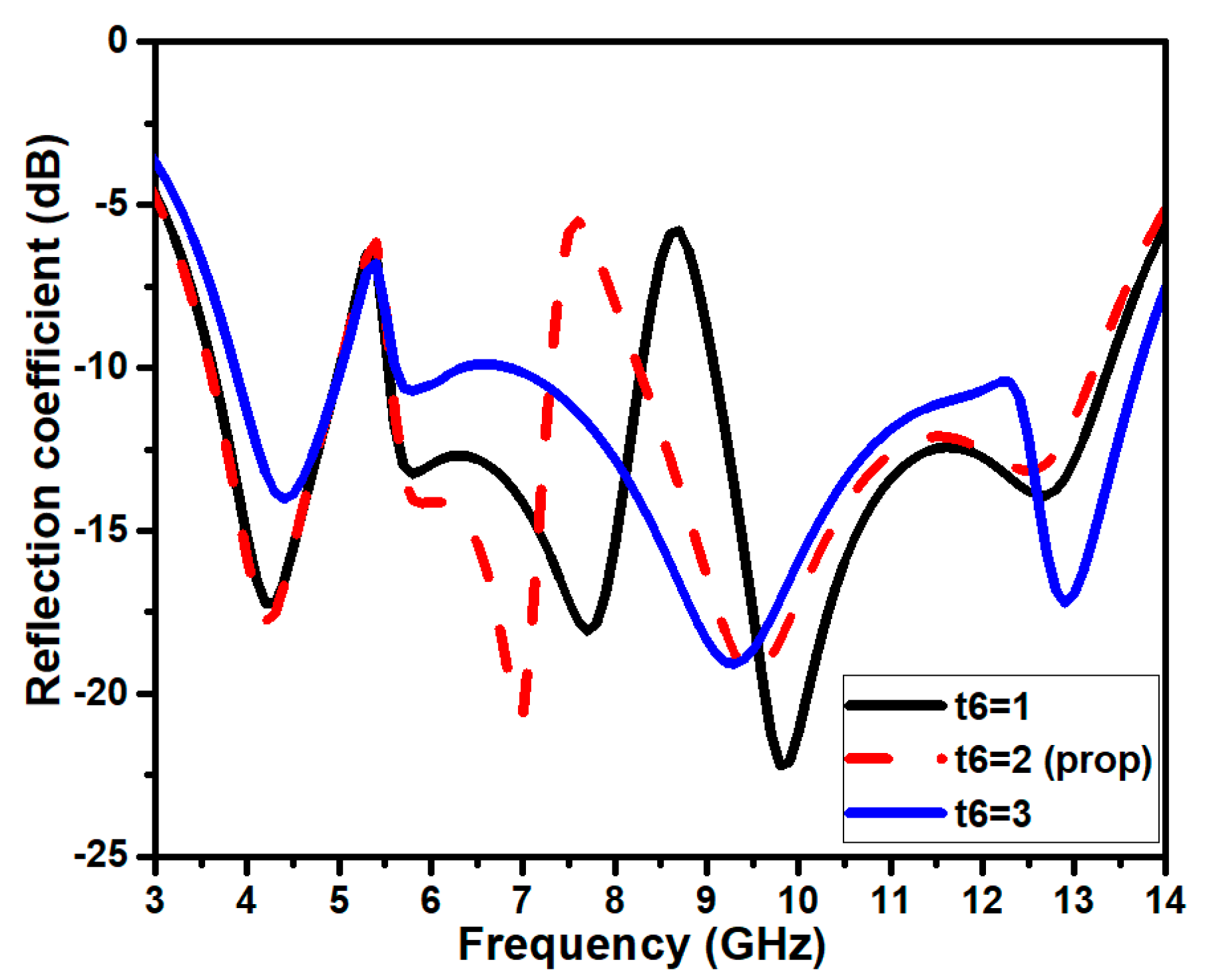
3. Parametric Analysis

The change in the dimensions of the antenna’s design and its impact on the antenna’s performance are examined through a parametric analysis. This segment depicts a detailed antenna structure analysis to attain the UWB and dual-band notch frequency features. First, to achieve the UWB frequency spectrum, the ground plane is lowered to less than a quarter of the entire ground plane. This process is carried out by simulating the design with a full ground plane, i.e., p6 = 16 mm, a length that exhibits no frequency range below −10 dB. Further, the length of p6 is reduced in a descending manner from 16, 13.6, 11.3, 8.9, 6.6, 4.2, and 1.9 mm, correspondingly, with a step of 2.35 mm. Every magnitude results in different S11 curves, as shown in Figure 6. From this figure, it can be observed that until reaching p6 = 6.6 mm, the reflection coefficient is not below −10 dB. The ground plane length of 1.9 mm shows an impedance bandwidth between 4 and 13.7 GHz. Consequently, to improve the bandwidth further in the UWB range, especially at a lower frequency, an arc shape is included at the edges of the ground plane. The optimal length of the rectangular slot (p7) on the ground plane is chosen by performing a parametric study. An initial value of p7 is chosen at 0.1 mm, and at an incremental step of 0.1 mm until reaching 0.5 mm, it varies, respectively. The value of p7 = 0.5 results in the no-frequency spectrum below −10 dB. The corresponding S11 curve is depicted in Figure 7. The optimal dimension of the rectangular slot’s width is found to be 0.2 mm, providing an impedance bandwidth of 113% in the frequency range of 3.7–13.3 GHz.
Second, inverted U-shaped slots are used to attain the frequency notching effect. The physical dimensions of these elements are realized by performing a parametric analysis. The inverted U-shaped notch is responsible for the first notch at the center frequency of 5.4 GHz. The initial dimensions of t1 and t2 are chosen to be 0.1 mm, and t3 = 6 mm. The S11 response for this configuration shows the frequency notching shifting towards the higher frequency after reaching 5.5 GHz. To attain the WLAN frequency band notch, the t1, t2, and t3 dimensions are simultaneously increased by 0.1 mm, 0.1 mm, and 1 mm, respectively. The corresponding S11 curves are depicted in Figure 8, Figure 9 and Figure 10. It can be witnessed from the figures that the optimum physical values of the inverted U-shaped slots were found to be t1 = 0.2 mm, t2 = 0.2 mm, and t3 = 8 mm, providing notching between the frequency range of 5–5.6 GHz. Similarly, the second notch is achieved by incorporating an inverted U-shaped slot. The optimum physical dimensions of the slot are found to be t4 = 0.5 mm, t5 = 0.4 mm, and t6 = 2 mm, resulting in the frequency notch from 7.3 to 8.3 GHz, as shown in Figure 11, Figure 12 and Figure 13.

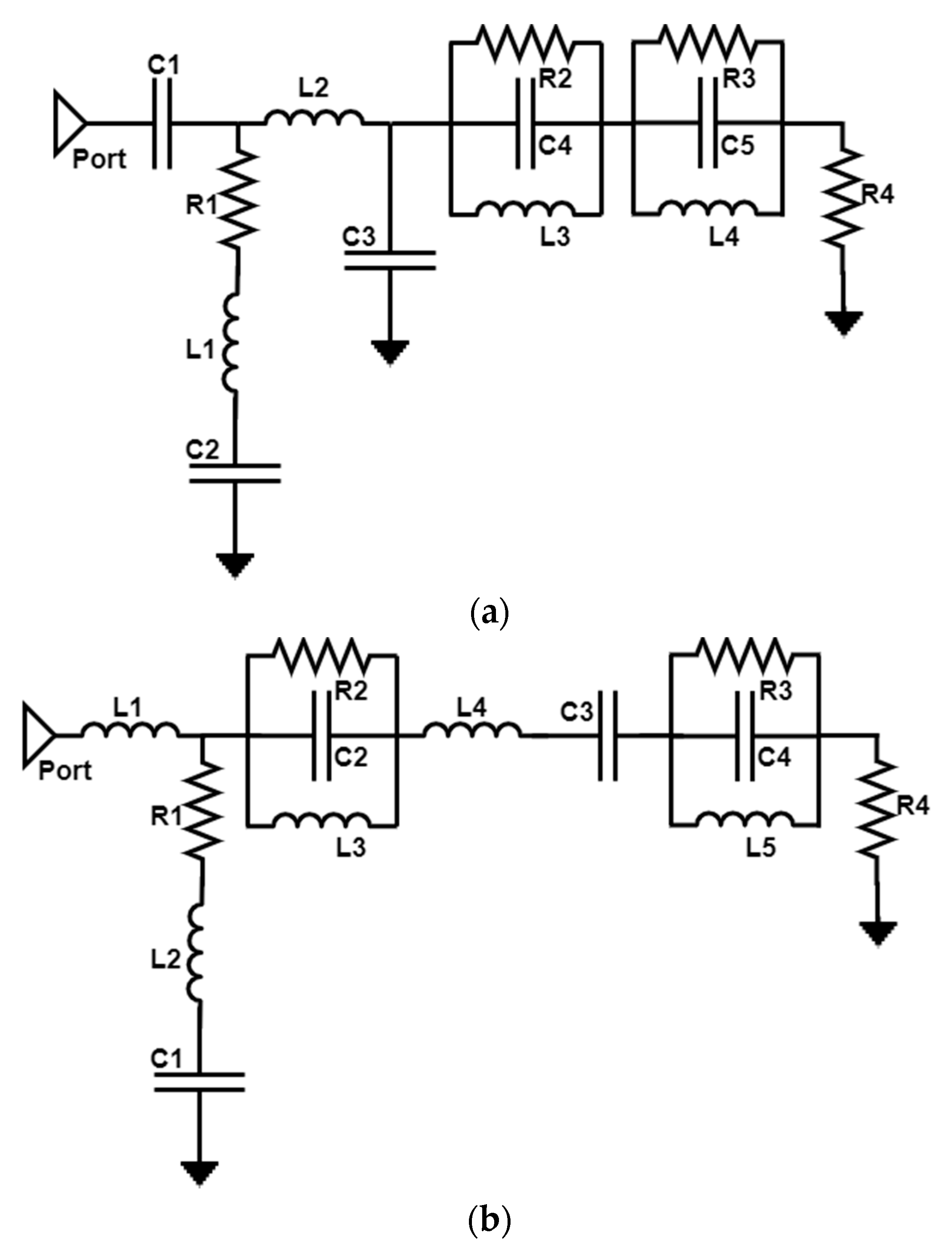
4. Antenna Modeling Using RLC Components
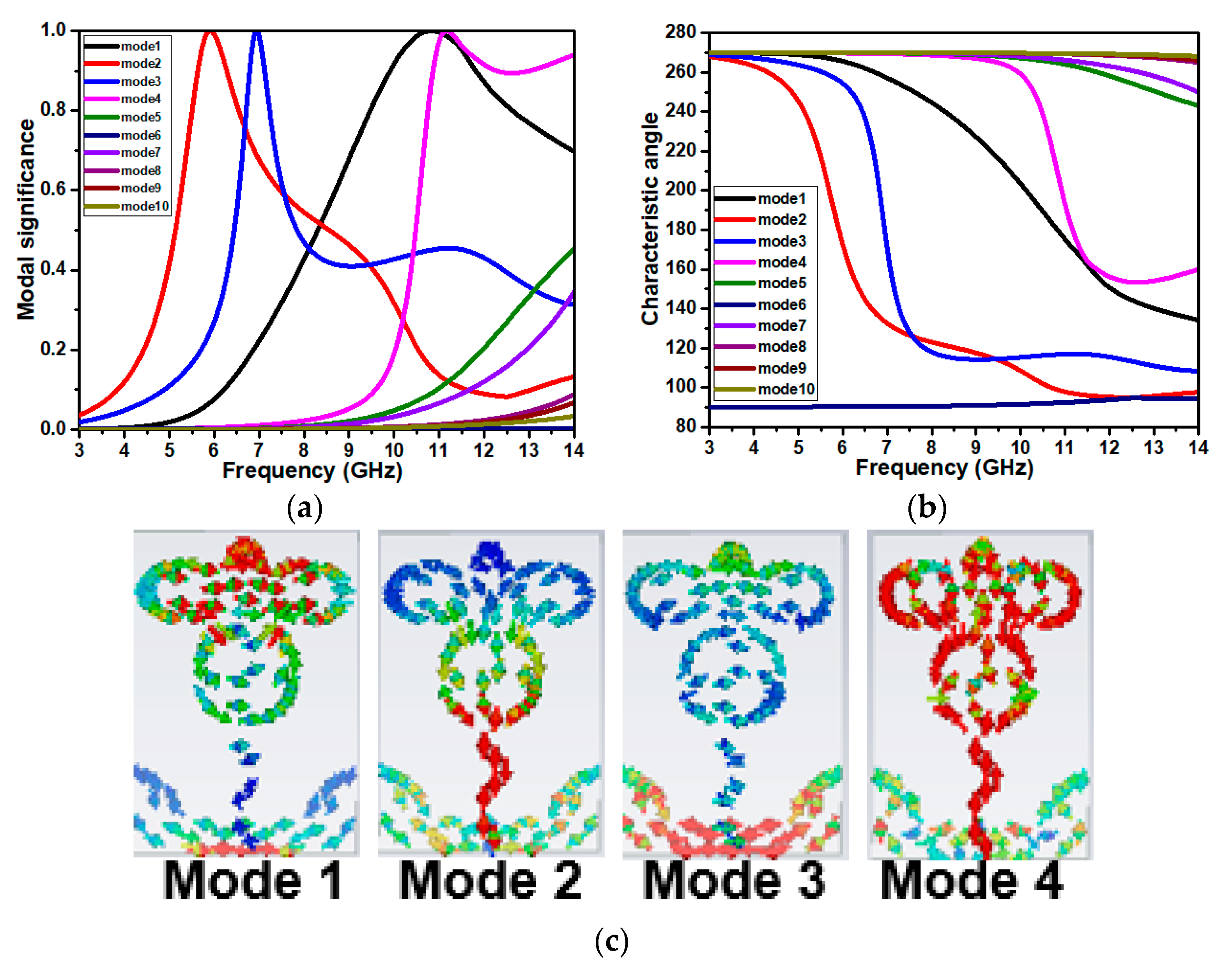
The transmitter and receiver in the communication system pose as an electrical system; therefore, analyzing the antenna as an equivalent circuit is useful for circuit simulations and time domain analysis. Such an electrical model can be highly beneficial in investigating the antenna’s integration with the transceivers. The circuit theory analyzes the antenna as a passive single-port network that imparts impedance to the source. The projected antenna equivalent circuit is modeled in AWR design environment 15, as depicted in Figure 14. The impedance model approach is used to build an analogous circuit model. [28]. A 50 Ω RF source is used to excite the input port. Different contiguous resonances generated by parallel resonators connected in series accomplish the wideband impedance matching. The UWB antenna exhibits two sharp resonances at 4.5 GHz and 8.5 GHz, and this is represented using two parallel RLCs connected in a series arrangement, as depicted in Figure 14a. The series RLC configuration resonates when the inductance and capacitance are equal, helping to tune applications. The series RLC provides a sharp curve at the resonating frequencies. The circuit arrangement used for the UWB antenna is modified to achieve an equivalent circuit to a dual-band notch UWB antenna. The RLC configuration used for achieving two notches is based on the impedance curve, and the associated circuit theory diagram is represented in Figure 14b.

5. CMA

The integration of the antenna with the radio frequency front-end transceivers necessitates a design metrics compromise that fulfills the application’s need. The CMA is one method for examining such a problem that uses classical electromagnetism to introduce the notion of the CMA [29,30]. The CMA generates an endless number of distinct current patterns that may be evaluated for the frequency of interest. According to the CMA, the arbitrary conducting plane has multiple distinctive modes, including orthogonal modal currents ( J i ) and weighted eigenvalues ( λ i ). The cumulative current is given in terms of ( J i ) and the modal weight coefficients ( β i ) by Equation (6):
  J = i = n N β i   J i         .
β i  is used to determine the impact of an individual eigencurrent on the total current and how it affects the overall electric field. The eigenvector signifies the excitation and radiation properties of the antenna while the eigenvalues indicate the magnitude of the capacitive and inductive energy storage, as illustrated in Table 3. The method of moment matrix (Z) links the eigenvalue and eigencurrent, as depicted in Equations (7) and (8):
Z = R + j X ,   and
X   J i     = λ i   R     J i     ,
where X and R represent the imaginary and real components of the impedance Z, respectively. The modal significance (MS) is a key CMA parameter that specifies every mode’s optimum normalized current performance and its effects on the radiation characteristics. The characteristic angle (CA) describes the phase difference between the antenna’s electric field and the surface current. The MS and CA ( α i   ) are computed using Equations (9) and (10), respectively. The proposed UWB antenna is simulated to study the physical insight of the structure through the CMA, as depicted in Figure 15a–c.
      M S = 1 1 + j λ i   ,   and
        α i   = 180 0 t a n 1 λ i     .
The CMA of the proposed antenna exhibits specific significant modes that contribute to the antenna’s radiation. The first four modes are relatively significant and contribute to the antenna performance. The eigencurrents are not affected by any source or excitation, but rather, by the structure and size of the antenna. The optimization of the geometry of the antenna by looking into the individual mode current helps in achieving a broader bandwidth and the required radiation properties. The substantial individual mode current contributes an antenna to achieve bidirectional and omnidirectional radiation patterns at the E- and H-planes, respectively.

6. Results and Discussions

This segment depicts the simulated and measured results of the projected UWB and UWB dual-band notched antennas for the S11, impedance, and radiation characteristics. Furthermore, detailed time-domain characteristics such as transfer function, phase response, group delay, fidelity factor, and equivalent circuit analysis are studied. The proposed microstrip-fed antennas are fabricated as shown in Figure 16. Ansoft HFSS simulators are utilized to optimize the design and develop good concordance among the simulated and measured results.

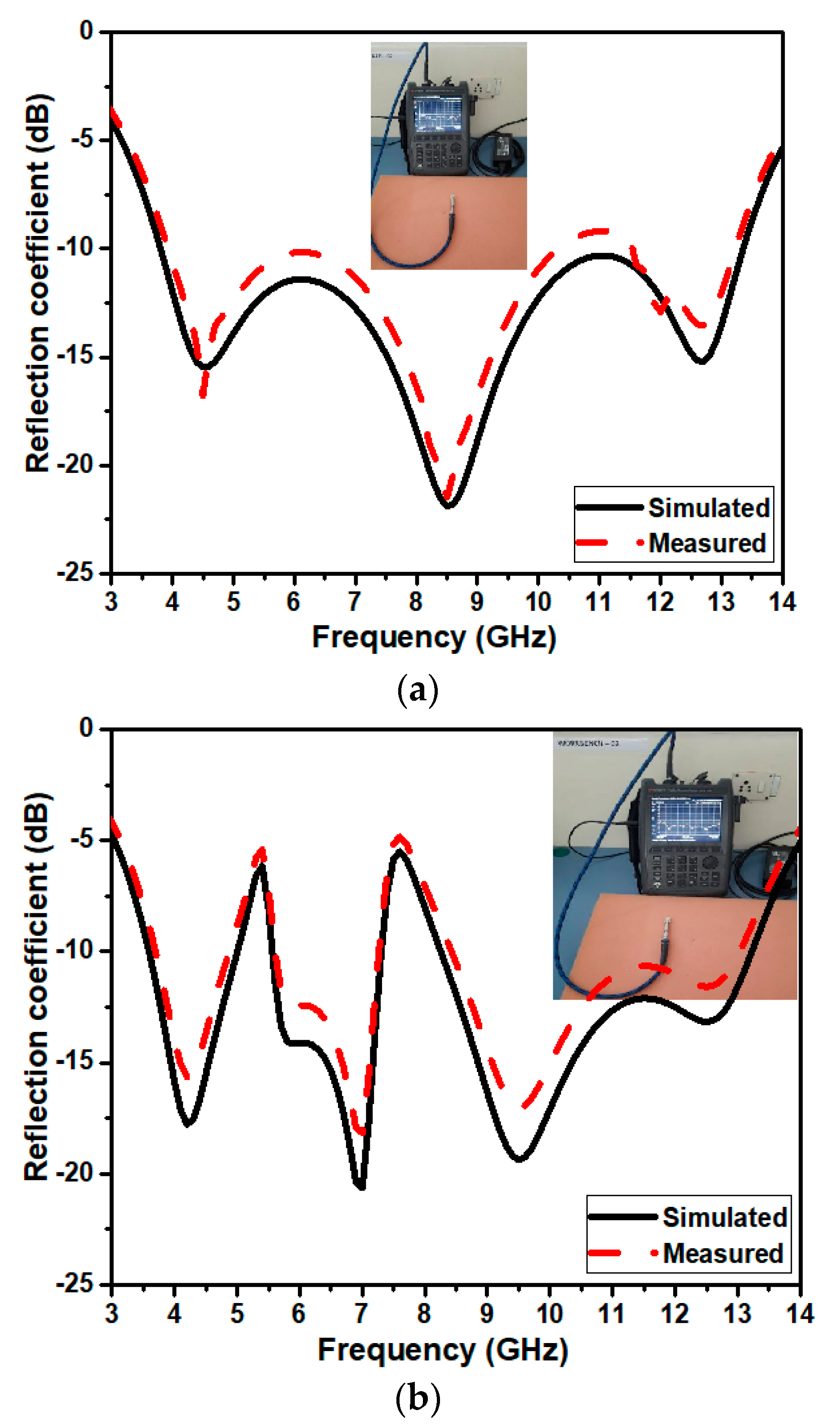
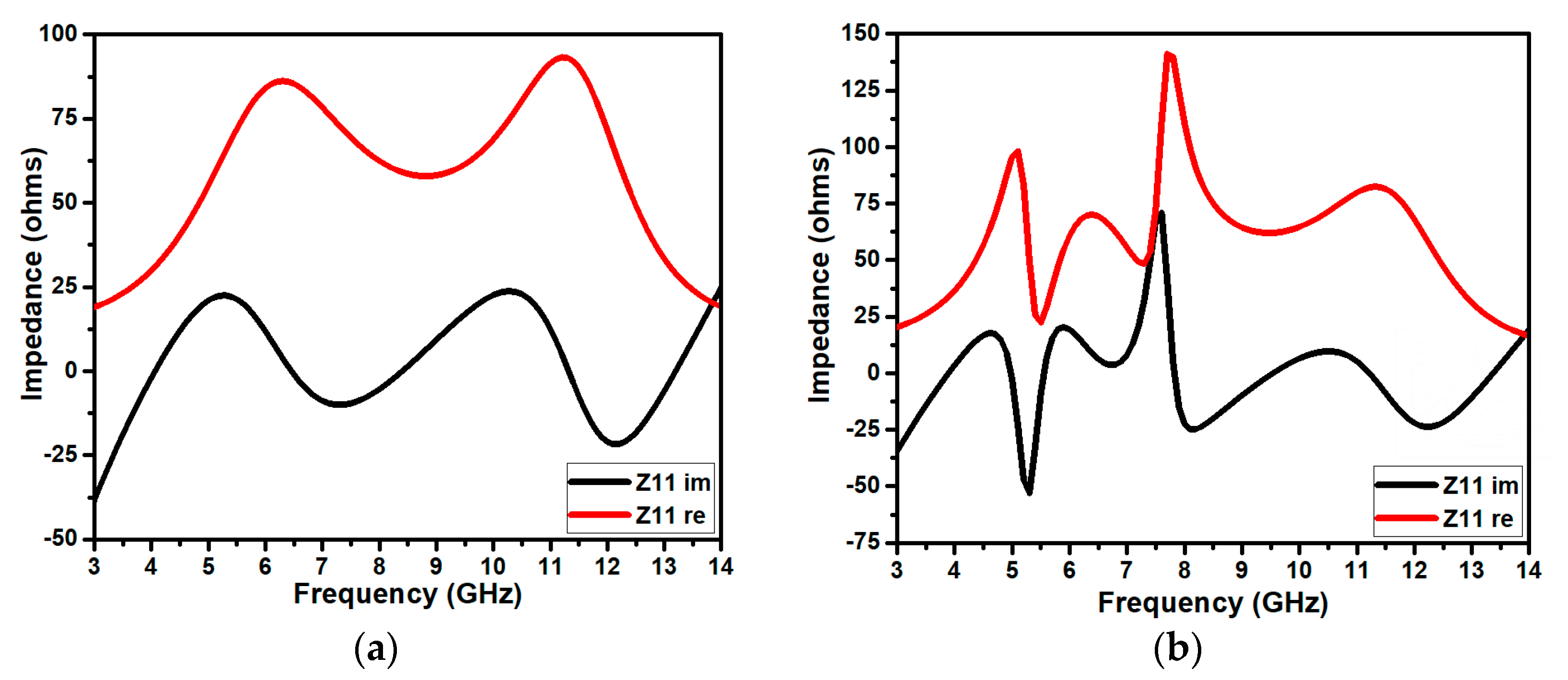
6.1. S-Parameters (S11) and Impedance (Z11)

Figure 17 illustrates the simulated and observed S11 curves of the UWB and dual-band UWB. It is evident that the projected UWB antenna structures have a measured (Keysight N9951A VNA is used) impedance bandwidth of approximately 113% between the range of 3.7 and 13.3 GHz. Conversely, the first notch is achieved between the frequencies of 5 and 5.6 GHz, filtering the IEEE 802.11, Wi-Fi, and WLAN bands. The second notch is achieved between the frequencies of 7.3 and 8.3 GHz, covering the complete X-band satellite communication. The measured results of the UWB band notches are in line with the simulation.
The impedance parameter (Z11) assists in identifying the operating frequency of the antenna element, which has only a resistive part and no reactive portion. The impedance curve of the projected UWB has a resistive part approximately equal to the 50 Ω and nearly 0 reactive components, as depicted in Figure 18a. Similarly, the dual-band notch antenna has nearly 50 Ω resistive parts and zero reactive components, respectively, except at the notched frequency bands. At the dual notch frequencies, the impedance has (98.25 − j22.89) Ω and (141.19 + j40.46) Ω, correspondingly, as depicted in Figure 18b.

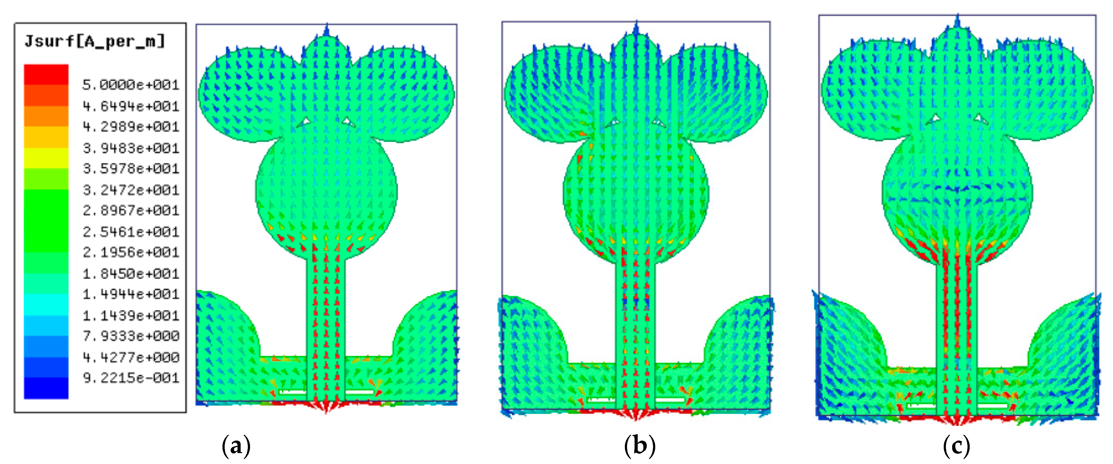
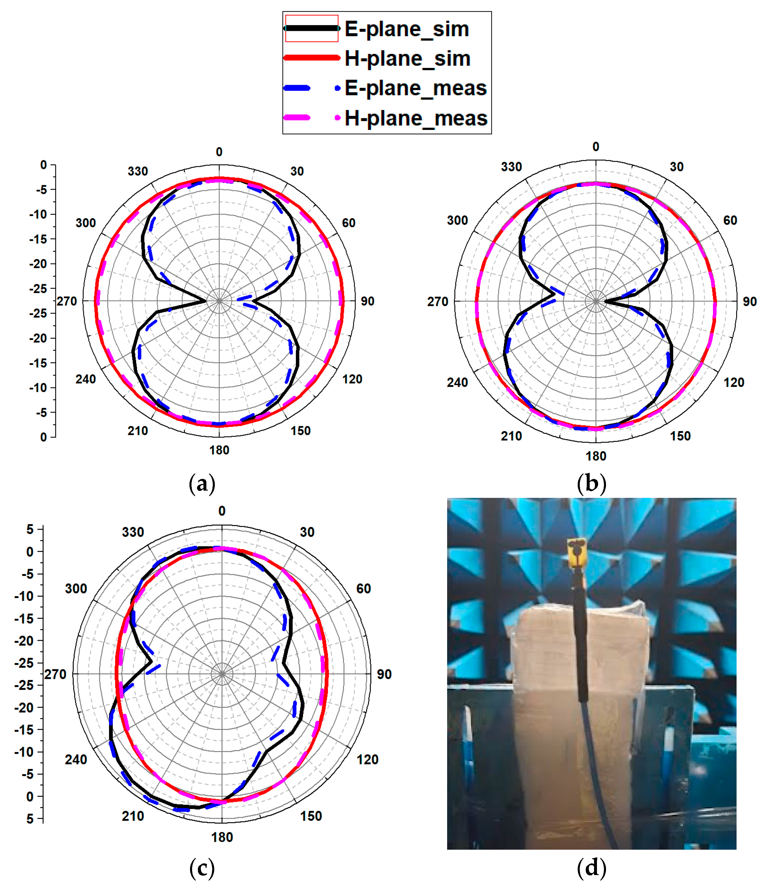
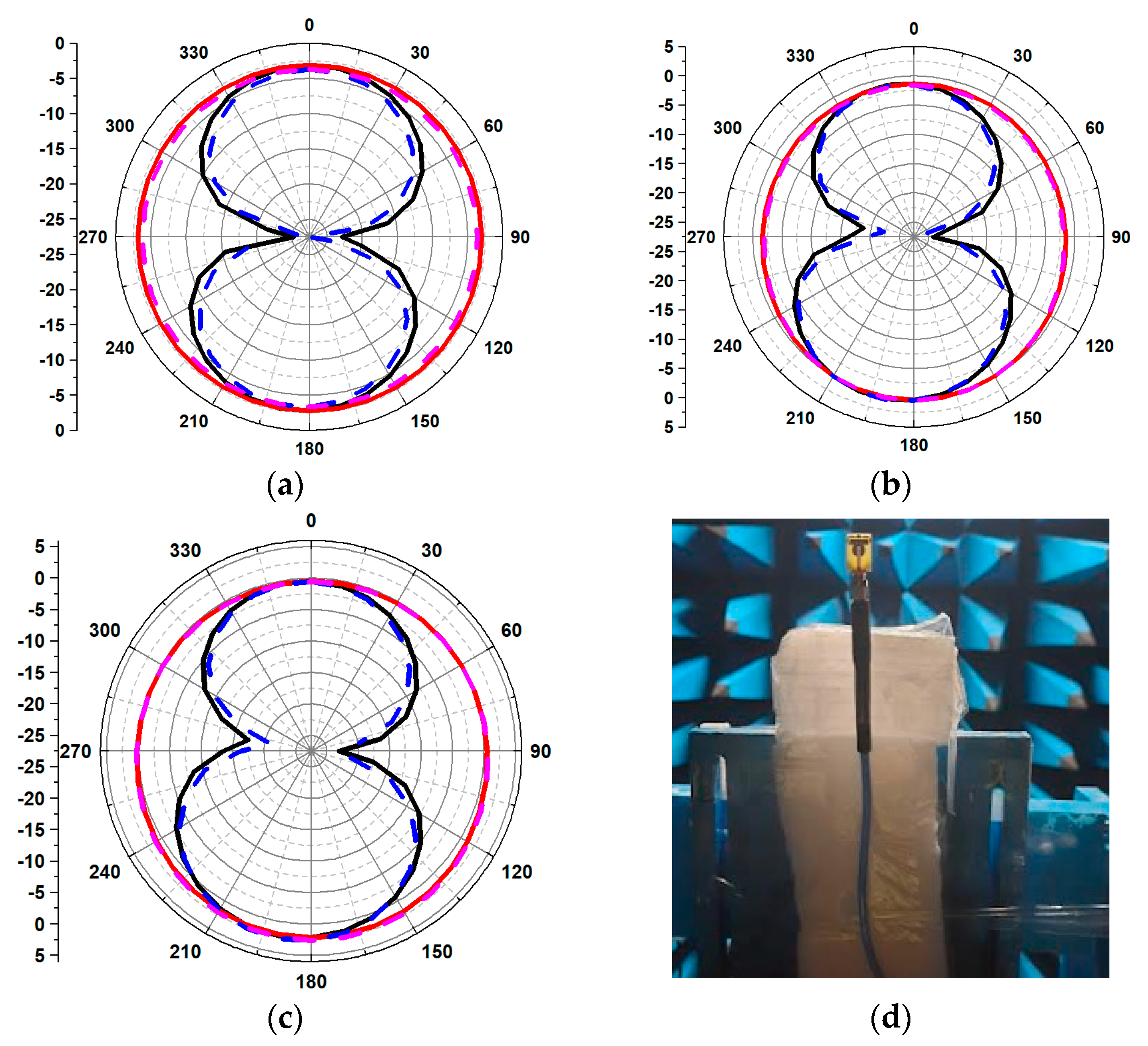
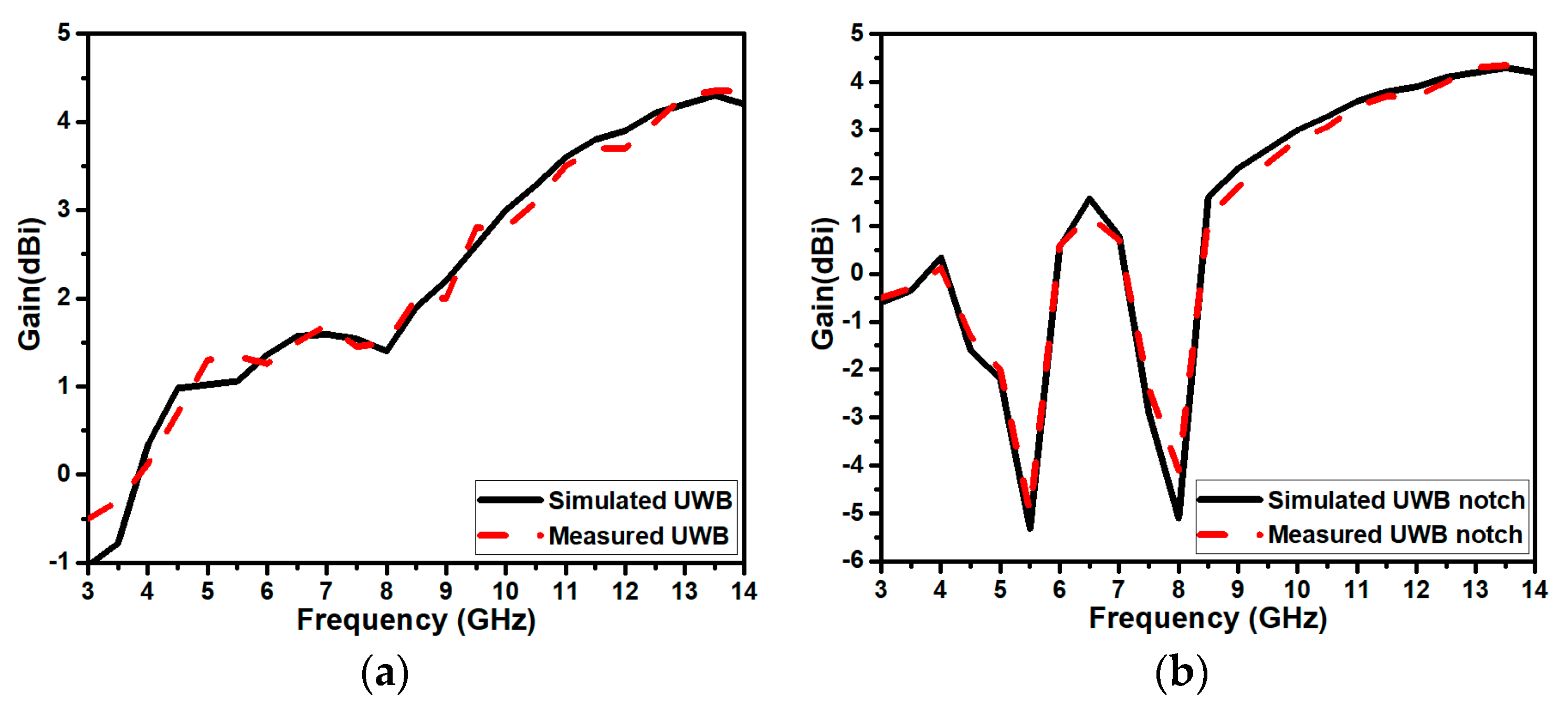
6.2. Radiation Characteristics

The radiation pattern analysis at the resonating frequencies is performed in the anechoic chamber. The radiation patterns of the projected UWB and UWB band notch antennas are performed at 4.5 GHz, 8.5 GHz, and 12.7 GHz and 4.2 GHz, 7 GHz, and 9.5 GHz, respectively. Because the antenna’s length and width are in the XY plane, the XZ and YZ planes serve as two primary planes, E and H. Figure 19 and Figure 20 show the computed and observed radiation patterns of the proposed UWB and UWB band notch antennas.
In the E-plane, both the antennas exhibit nearly bidirectional and omnidirectional patterns in the H-plane. A slight deviation is witnessed in the measured results. This may be because of the SMA connector loss, fabrication, and soldering influence. Figure 21 depicts the simulated and observed gains against the frequency curves of the UWB and dual-band notch UWB antennas. It can be noticed from the figure that the first notch frequency gain is well below −5 dB, and for the second notch, it is also below −5 dB, indicating the effectiveness of the notch structures.

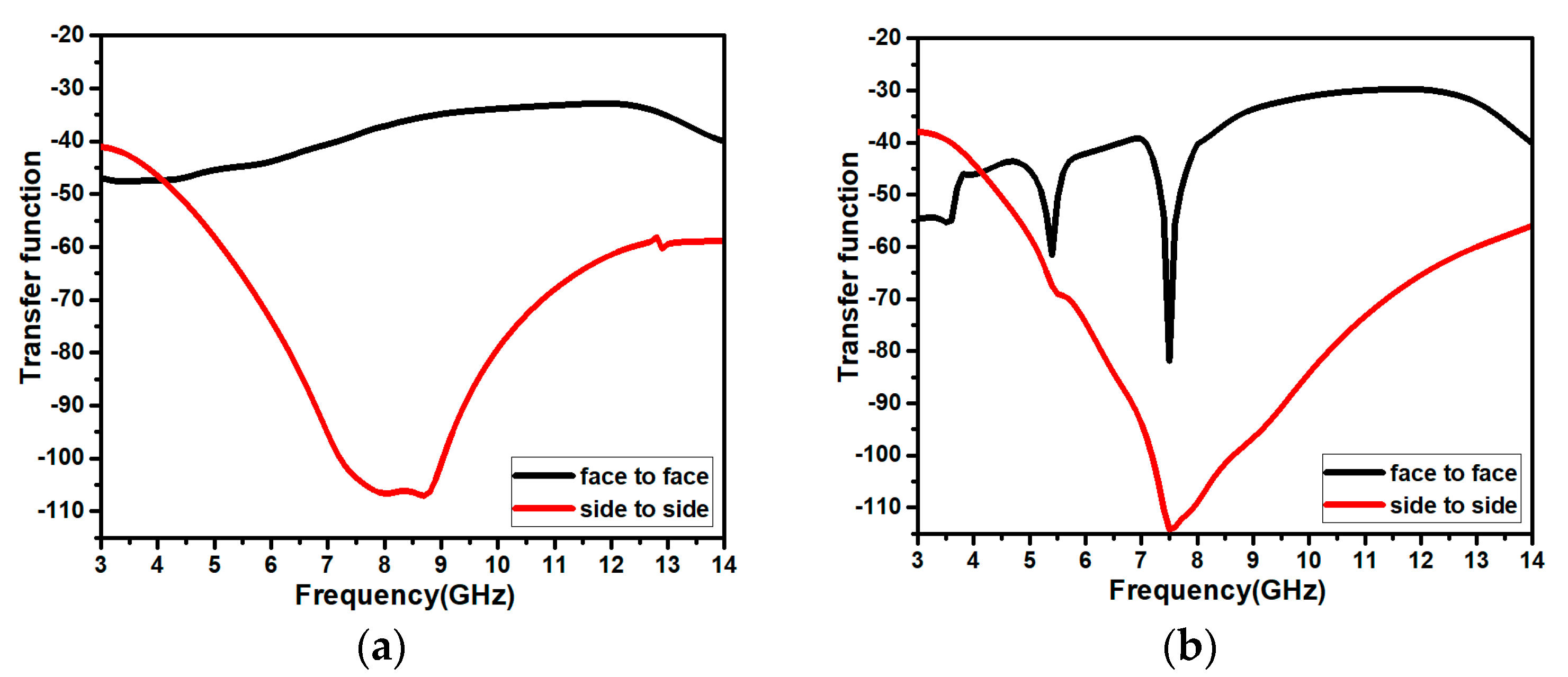
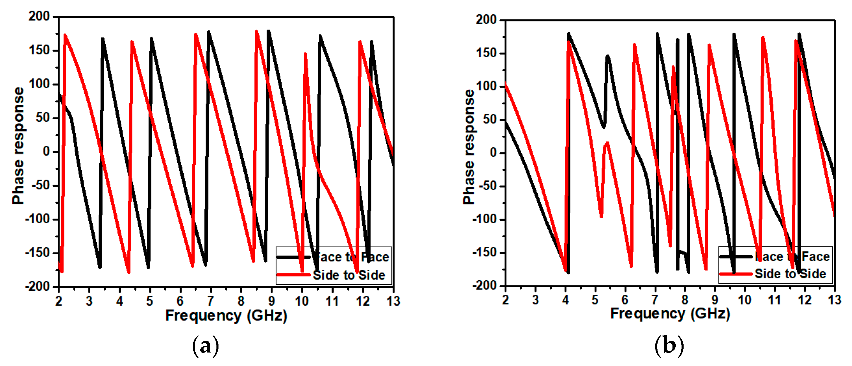
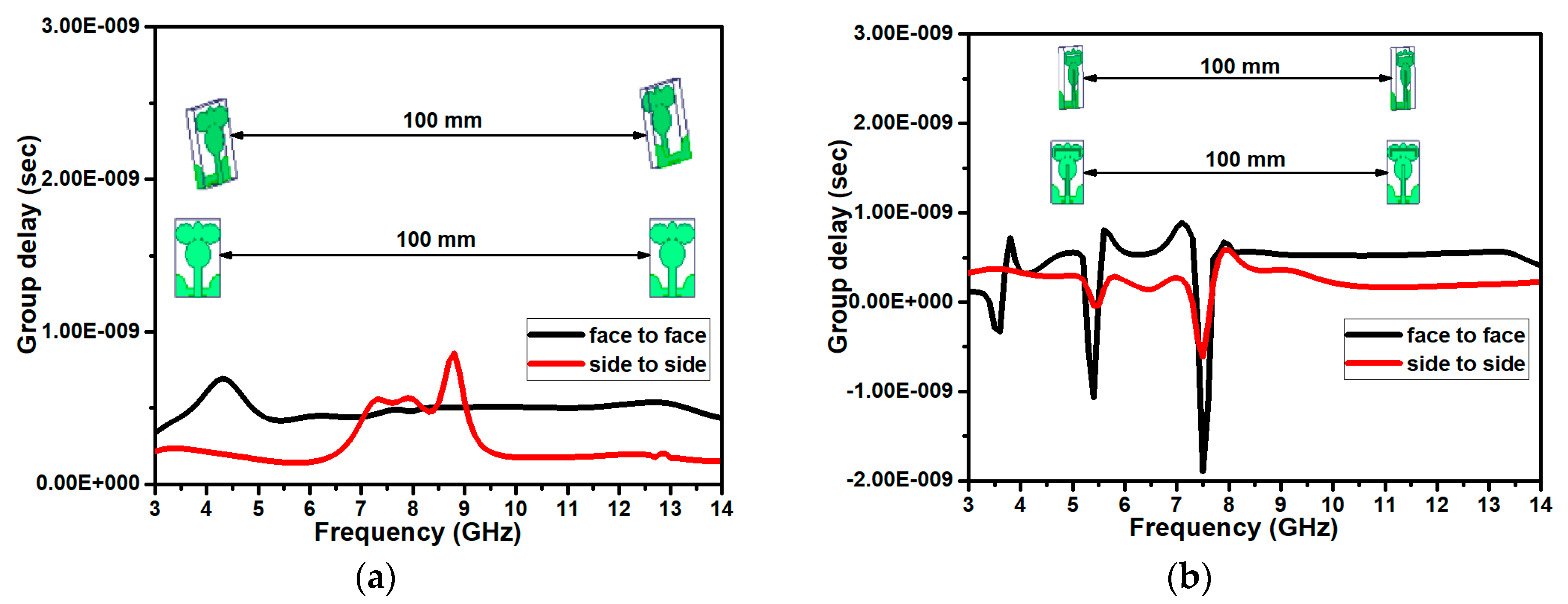
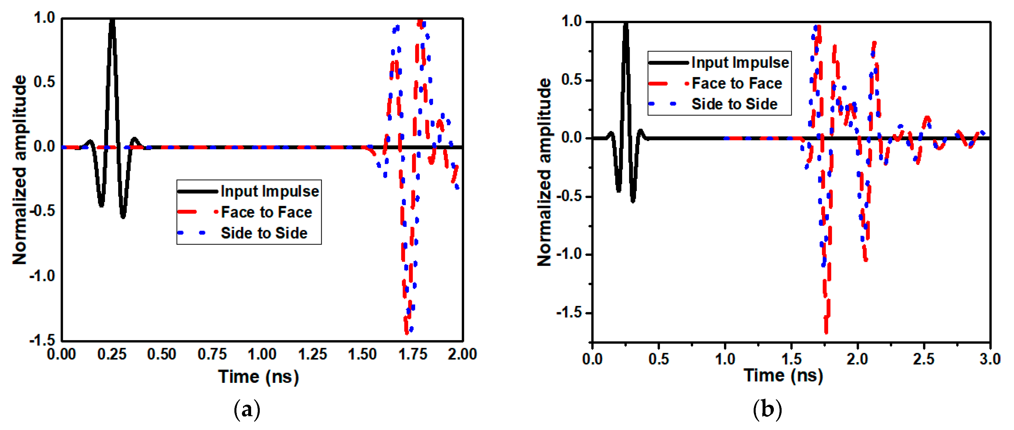
6.3. Time-Domain Analysis

The federal communication commission’s (FCC) specifications for designing ultrawideband (UWB) antennas necessitate additional performance parameters beyond those required for standard antennas. The UWB provides an unlicensed 7.5 GHz frequency band ranging from 3.1 to 10.6 GHz for short-range connectivity. A UWB transmits and receives signals using short pulses for this intent. Due to the obvious transmission link and distance, signal distortion and dispersion are possible during communication. The transfer function, phase response, group delay, and fidelity factors need to be examined for the linear phase between the input and output signals. To investigate the aforementioned metrics, two identically designed antennas are aligned face-to-face and side-to-side, situated at a distance of 100 mm apart. The transfer function curves of both the UWB and the UWB band notch are depicted in Figure 22. The transfer function/isolation describes the amount of correlation between the elements. The UWB and UWB band notch antennas have isolation values of less than −40 dB and −35 dB throughout the antennas’ operating frequency in both the face-to-face and side-to-side arrangements. These values indicate that the antennas have negligible correlation effects. The phase response curves indicate linearity in the transmitted and received signals. The phase responses of the projected UWB and UWB band notch are depicted in Figure 23. It can be witnessed that there is a negligible variation in the peaks of the phase response curve except for the frequency band, which is filtered out. The phase response curve signifies the linear phase between the input and output signals.
A further important time-domain parameter is the group delay, which is calculated quantitatively as the negative derivative of the phase variation in accordance with the angular frequency. As the signal propagates, it experiences amplitude and phase disturbance. The input signal may have numerous frequency components. For such signals, the group delay signifies the phase linearity of the system, and it is described by Equation (11). The acceptable value of the group delay is less than 1 ns.
τ g ω = d φ ω d ω
The group delays of the projected antennas are depicted in Figure 24, and they are less than 1 ns in both configurations—side-to-side and face-to-face—except for the notched frequency bands. The transmitted and received pulse shapes are analyzed using another significant metric, the fidelity factor (FF). This parameter signifies the amount of pulse shape distortion, not the amplitude of the pulse. The fidelity factors for the projected antennas are computed in both the face-to-face and side-to-side orientations. The input and out signals are normalized to ensure that the signals’ shapes are examined, and they are depicted in Figure 25. The similarity between the input and output signals is computed using Equations (12)–(14), and they are tabulated in Table 4.
T s n = T s t T s t 2 d t                         ,
R s n = R s t R s t 2 d t ,   and
  F F = max T s n t     R s n t + τ d t .

6.4. Comparative Analysis

In Table 5, the performance parameters of the projected UWB with two frequency band notch antennas are compared to those of the previously stated designs. The projected design has physical dimensions that are comparatively small, a broader impedance bandwidth, and good time-domain characteristics.

7. Conclusions

A novel, simple, and compact dual-band notch monopole antenna operating in the UWB range is designed, developed, and tested for efficacy. The proposed design combines circular and ellipse structures to provide a measured impedance bandwidth of between 3.7 and 13.3 GHz. Contrarily, the ground plane, which is lowered to less than a quarter of the substrate length, is responsible for the lower resonating frequency. The dual-band notching is performed by carving two inverted U-shaped slots on the radiator, rejecting the frequency band from 5 to 5.6 GHz and from 7.3 to 8.3 GHz, respectively. The lower and upper notches cover the existing narrowbands such as WLAN, IEEE 802.11/a/b/j/n/ac/ax, and the entire uplink–downlink of X-band satellite communication. In addition to the frequency domain analysis, the projected design is examined for time-domain metrics such as FF, group delay, phase response, and transfer function. The equivalent circuit is modeled and analyzed. The simulated and measured results are almost identical, and a performance comparison with existing structures makes it appropriate for UWB wireless applications. Furthermore, the results of the developed antenna show that it may be transformed into a MIMO antenna to boost channel capacity for future work.

Author Contributions

Conceptualization, P.K. (Praveen Kumar), M.P.M., T.A., P.K. (Pradeep Kumar), M.G.N.A. and V.S.; methodology, P.K. (Praveen Kumar), M.P.M., T.A., P.K. (Pradeep Kumar), M.G.N.A. and V.S.; software, P.K. (Praveen Kumar) and T.A.; validation, P.K. (Praveen Kumar), M.P.M., T.A., P.K. (Pradeep Kumar), M.G.N.A. and V.S.; writing—original draft preparation, P.K. (Praveen Kumar) and T.A.; writing—review and editing, P.K. (Praveen Kumar), M.P.M., T.A., P.K. (Pradeep Kumar) and M.G.N.A.; supervision, T.A. and M.P.M. All authors have read and agreed to the published version of the manuscript.

Funding

This research received no external funding.

Data Availability Statement

The data are contained within the article.

Conflicts of Interest

The authors declare no conflict of interest.

References

  1. Adame, B.O.; Salau, A.O. Genetic algorithm based optimum finger selection for adaptive minimum mean square error rake receivers discrete sequence-CDMA ultra-wide band systems. Wirel. Pers. Commun. 2022, 123, 1537–1551. [Google Scholar] [CrossRef]
  2. Ghosh, D.; De, A.; Taylor, M.C.; Sarkar, T.K.; Wicks, M.C.; Mokole, E.L. Transmission and reception by ultra-wideband (UWB) antennas. IEEE Antennas Propag. Mag. 2006, 48, 67–99. [Google Scholar] [CrossRef]
  3. Galvan-Tejada, G.M.; Peyrot-Solis, M.A.; Jardón Aguilar, H. Ultra Wideband Antennas: Design, Methodologies, and Performance; CRC Press: Boca Raton, FL, USA, 2019. [Google Scholar]
  4. Kumar, P.; Pai, M.M.; Ali, T. Ultrawideband antenna in wireless communication: A review and current state of the art. Telecommun. Radio Eng. 2020, 79, 929–942. [Google Scholar] [CrossRef]
  5. Rahman, M.; Haider, A.; Naghshvarianjahromi, M. A systematic methodology for the time-domain ringing reduction in UWB band-notched antennas. IEEE Antennas Wirel. Propag. Lett. 2020, 19, 482–486. [Google Scholar] [CrossRef]
  6. Kumar, P.; Ali, T.; Mm, M.P. Characteristic mode analysis-based compact dual band-notched UWB MIMO antenna loaded with neutralization line. Micromachines 2022, 13, 1599. [Google Scholar] [CrossRef]
  7. Modak, S.; Khan, T.; Laskar, R.H. Penta-notched UWB monopole antenna using EBG structures and fork-shaped slots. Radio Sci. 2020, 55, 1–11. [Google Scholar] [CrossRef]
  8. Kumar, P.; Ali, T.; Pai, M.M. Electromagnetic Metamaterials: A New Paradigm of Antenna Design. IEEE Access 2021, 9, 18722–18751. [Google Scholar] [CrossRef]
  9. Awan, W.A.; Choi, D.M.; Hussain, N.; Elfergani, I.; Park, S.G.; Kim, N. A frequency selective surface loaded uwb antenna for high gain applications. CMC-Comput. Mater. Contin. 2022, 73, 6169–6180. [Google Scholar]
  10. Kumar, P.; Pai, M.M.M.; Ali, T. Design and analysis of multiple antenna structures for ultrawide bandwidth. Telecommun. Radio Eng. 2021, 80, 13. [Google Scholar] [CrossRef]
  11. Kumar, P.; Ali, T.; Pai, M.M. A compact highly isolated two-and four-port ultrawideband Multiple Input and Multiple Output antenna with Wireless LAN and X-band notch characteristics based on Defected Ground Structure. Int. J. Commun. Syst. 2022, 35, e5331. [Google Scholar] [CrossRef]
  12. Emadian, S.R.; Ahmadi-Shokouh, J. Study on frequency and time domain properties of novel triple band notched UWB antenna in indoor propagation channel. Int. J. RF Microw. Comput.-Aided Eng. 2018, 28, e21428. [Google Scholar] [CrossRef]
  13. Ali, A.; Tong, J.; Iqbal, J.; Illahi, U.; Rauf, A.; Rehman, S.U.; Ghoniem, R.M. Mutual coupling reduction through defected ground structure in circularly polarized, dielectric resonator-based MIMO antennas for sub-6 GHz 5G applications. Micromachines 2022, 13, 1082. [Google Scholar] [CrossRef] [PubMed]
  14. Iqbal, J.; Illahi, U.; Khan, M.A.; Rauf, A.; Ali, E.M.; Bari, I.; Dalarsson, M. A novel single-fed dual-band dual-circularly polarized dielectric resonator antenna for 5G Sub-6GHz applications. Appl. Sci. 2022, 12, 5222. [Google Scholar] [CrossRef]
  15. Guha, D.; Kumar, C. Microstrip Patch versus Dielectric Resonator Antenna Bearing All Commonly Used Feeds: An experimental study to choose the right element. IEEE Antennas Propag. Mag. 2016, 58, 45–55. [Google Scholar] [CrossRef]
  16. NejatiJahromi, M.; NagshvarianJahromi, M.; Rahman, M. A New Compact Planar Antenna for Switching between UWB, Narrow Band and UWB with Tunable-notch Behaviors for UWB and WLAN Applications. Appl. Comput. Electromagn. Soc. J. 2018, 33, 400–406. [Google Scholar]
  17. Gao, G.; Hu, B.; He, L.; Wang, S.; Yang, C. Investigation of a reconfigurable dual notched UWB antenna by conceptual circuit model and time-domain characteristics. Microw. Opt. Technol. Lett. 2017, 59, 1326–1332. [Google Scholar] [CrossRef]
  18. Mewara, H.S.; Deegwal, J.K.; Sharma, M.M. A slot resonators based quintuple band-notched Y-shaped planar monopole ultra-wideband antenna. AEU-Int. J. Electron. Commun. 2018, 83, 470–478. [Google Scholar] [CrossRef]
  19. Tang, Z.; Zhan, J.; Wu, X.; Xi, Z.; Chen, L.; Hu, S. Design of a compact UWB-MIMO antenna with high isolation and dual band-notched characteristics. J. Electromagn. Waves Appl. 2020, 34, 500–513. [Google Scholar] [CrossRef]
  20. Kumar, S.; Lee, G.H.; Kim, D.H.; Mohyuddin, W.; Choi, H.C.; Kim, K.W. Multiple-input-multiple-output/diversity antenna with dual band-notched characteristics for ultra-wideband applications. Microw. Opt. Technol. Lett. 2020, 62, 336–345. [Google Scholar] [CrossRef]
  21. Liu, L.; Cheung, S.W.; Yuk, T.I. Compact MIMO antenna for portable UWB applications with band-notched characteristic. IEEE Trans. Antennas Propag. 2015, 63, 1917–1924. [Google Scholar] [CrossRef]
  22. Zhu, J.; Li, S.; Feng, B.; Deng, L.; Yin, S. Compact dual-polarized UWB quasi-self-complementary MIMO/diversity antenna with band-rejection capability. IEEE Antennas Wirel. Propag. Lett. 2015, 15, 905–908. [Google Scholar] [CrossRef]
  23. Kang, L.; Li, H.; Wang, X.; Shi, X. Compact offset microstrip-fed MIMO antenna for band-notched UWB applications. IEEE Antennas Wirel. Propag. Lett. 2015, 14, 1754–1757. [Google Scholar] [CrossRef]
  24. Chattha, H.T.; Latif, F.; Tahir, F.A.; Khan, M.U.; Yang, X. Small-sized UWB MIMO antenna with band rejection capability. IEEE Access 2019, 7, 121816–121824. [Google Scholar] [CrossRef]
  25. Tang, T.C.; Lin, K.H. An ultrawideband MIMO antenna with dual band-notched function. IEEE Antennas Wirel. Propag. Lett. 2014, 13, 1076–1079. [Google Scholar] [CrossRef]
  26. Tiwari, R.N.; Singh, P.; Kanaujia, B.K. A compact UWB MIMO antenna with neutralization line for WLAN/ISM/mobile applications. Int. J. RF Microw. Comput.-Aided Eng. 2019, 29, e21907. [Google Scholar] [CrossRef]
  27. Balanis, C.A. Antenna Theory: Analysis and Design; John Wiley & Sons: Hoboken, NJ, USA, 2015. [Google Scholar]
  28. Meena, M.L.; Kumar, M.; Parmar, G.; Meena, R.S. Design analysis and modeling of directional UWB antenna with elliptical slotted ground structure for applications in C-& X-bands. Prog. Electromagn. Res. C 2016, 63, 193–207. [Google Scholar]
  29. Garbacz, R.J. Modal expansions for resonance scattering phenomena. Proc. IEEE 1965, 53, 856–864. [Google Scholar] [CrossRef]
  30. Adams, J.J.; Genovesi, S.; Yang, B.; Antonino-Daviu, E. Antenna Element Design Using Characteristic Mode Analysis: Insights and research directions. IEEE Antennas Propag. Mag. 2022, 64, 32–40. [Google Scholar] [CrossRef]
  31. Kaur, K.; Kumar, A.; Sharma, N. Sprocket gear wheel shaped printed monopole ultra-wideband antenna with band notch characteristics: Design and measurement. Int. J. RF Microw. Comput.-Aided Eng. 2022, 32, e22989. [Google Scholar] [CrossRef]
  32. Kumar, G.; Singh, D.; Kumar, R. A planar CPW fed UWB antenna with dual rectangular notch band characteristics incorporating U-slot, SRRs, and EBGs. Int. J. RF Microw. Comput.-Aided Eng. 2021, 31, e22676. [Google Scholar] [CrossRef]
  33. Abbas, A.; Hussain, N.; Jeong, M.J.; Park, J.; Shin, K.S.; Kim, T.; Kim, N. A rectangular notch-band UWB antenna with controllable notched bandwidth and centre frequency. Sensors 2020, 20, 777. [Google Scholar] [CrossRef] [PubMed]
  34. Ranjan, P.; Kumar, A. Circularly polarized ultra–wide band filtering antenna with controllable band-notch for wireless communication system. AEU-Int. J. Electron. Commun. 2021, 135, 153738. [Google Scholar] [CrossRef]
  35. Kaur, K.; Kumar, A.; Sharma, N. Split Ring Slot Loaded Compact CPW-Fed Printed Monopole Antennas for Ultra-Wideband Applications with Band Notch Characteristics. Prog. Electromagn. Res. C 2021, 110, 39–54. [Google Scholar] [CrossRef]
  36. Devana, V.N.; Satyanarayana, V.; Lakshmi, A.V.; Sukanya, Y.; Kumar, C.; Ponnapalli, V.L.N.; Jagadeesh Babu, K. A novel compact fractal UWB antenna with dual band notched characteristics. Analog. Integr. Circuits Signal Process. 2022, 110, 349–360. [Google Scholar] [CrossRef]
  37. Puri, S.C.; Das, S.; Tiary, M.G. UWB monopole antenna with dual-band-notched characteristics. Microw. Opt. Technol. Lett. 2020, 62, 1222–1229. [Google Scholar] [CrossRef]
  38. Koteswara Rao Devana, V.N.; Maheswara Rao, A. A compact fractal dual high frequency band notched UWB antenna with a novel SC-DGS. Analog. Integr. Circuits Signal Process. 2021, 107, 145–153. [Google Scholar] [CrossRef]
  39. Medkour, H.; Cheniti, M.; Narbudowicz, A.; Das, S.; Vandelle, E.; Vuong, T.P. Coplanar waveguide-based ultra-wide band antenna with switchable filtering of WiMAX 3.5 GHz and WLAN 5 GHz signals. Microw. Opt. Technol. Lett. 2020, 62, 2398–2404. [Google Scholar] [CrossRef]
Figure 1. UWB antenna. (a) Antenna evolution representing the radiator (left) and ground pane (right) in each antenna configuration. (b) Reflection coefficient curve.
Jsan 12 00037 g001
Figure 2. Geometry details of the proposed UWB antenna: (a) radiator, and (b) ground plane.
Jsan 12 00037 g002
Figure 3. Geometry details of the proposed UWB dual-band notch antenna.
Jsan 12 00037 g003
Figure 4. The simulated current distribution of the UWB antenna at (a) 4.5 GHz, (b) 8.5 GHz, and (c) 12.7 GHz.
Jsan 12 00037 g004
Figure 5. The simulated current distribution of UWB band notch antenna at (a) 5.4 GHz, and (b) 7.6 GHz.
Jsan 12 00037 g005
Figure 6. The length of the ground plane (p6) analyzed for optimal value.
Jsan 12 00037 g006
Figure 7. The width of the rectangular slot on the ground plane is varied from 0.1 mm to 0.5 mm.
Jsan 12 00037 g007
Figure 8. The parameter t1 of the inverted U-shaped slot on the feedline is varied for choosing the ideal values.
Jsan 12 00037 g008
Figure 9. The parameter t2 of the inverted U-shaped slot on the feedline is varied for choosing the ideal values.
Jsan 12 00037 g009
Figure 10. The parameter t3 of the inverted U-shaped slot on the feedline is varied for choosing the ideal values.
Jsan 12 00037 g010
Figure 11. The parameter t4 of the inverted U-shaped slot on the radiator is varied for choosing the ideal values.
Jsan 12 00037 g011
Figure 12. The parameter t5 of the inverted U-shaped slot on the radiator is varied for choosing the ideal values.
Jsan 12 00037 g012
Figure 13. The parameter t6 of the inverted U-shaped slot on the radiator is varied for choosing the ideal values.
Jsan 12 00037 g013
Figure 14. The antenna equivalent circuit using lumped elements. (a) UWB: resistors (Ω): R1 = 1, R2 = 21, R3 = 3 K, and R4 = 50; inductors (nH): L1 = 12.3, L2 = 1.4, L3 = 0.254, and L4 = 0.79; and capacitors (pF): C1 = 0.79, C2 = 2, C3 = 0.25, C4 = 0.2, and C5 = 0.09. (b) UWB band notch: resistors (Ω): R1 = 3.8 K, R2 = 5 K, R3 = 3 K, and R4 = 50; inductors (nH): L1 = 1.31, L2 = 1, L3 = 0.112, L4 = 0.032, and L4 = 0.5; and capacitors (pF): C1 = 1, C2 = 6.3, C3 = 0.63, and C4 = 0.78.
Jsan 12 00037 g014
Figure 15. The CMA of the proposed UWB antenna at the center frequency: (a) MS, (b) CA, and (c) the first four significant modes of the current distribution.
Jsan 12 00037 g015
Figure 16. Prototypes of the proposed antenna designs: (a) UWB antenna, and (b) UWB band notch antenna.
Jsan 12 00037 g016
Figure 17. S11 curves of the (a) UWB and (b) UWB band notch antennas.
Jsan 12 00037 g017
Figure 18. Impedance curves of the (a) UWB and (b) UWB band notch.
Jsan 12 00037 g018
Figure 19. Simulated and measured radiation patterns of the UWB antennas. (a) 4.5 GHz, (b) 8.5 GHz, and (c) 12.7 GHz, and (d) the measurement setup.
Jsan 12 00037 g019
Figure 20. Simulated and measured radiation patterns of the UWB notch antenna. (a) 4.2 GHz, (b) 7 GHz, and (c) 9.5 GHz, and (d) the measurement setup.
Jsan 12 00037 g020
Figure 21. Gain versus frequency curves of the (a) UWB and (b) dual-band notch antennas.
Jsan 12 00037 g021
Figure 22. The transfer functions of the antennas: (a) UWB, and (b) UWB band notch.
Jsan 12 00037 g022
Figure 23. Phase responses of the antennas: (a) UWB, and (b) UWB band notch.
Jsan 12 00037 g023
Figure 24. The group delay of the antennas: (a) UWB, and (b) UWB band notch.
Jsan 12 00037 g024
Figure 25. Normalized inputs and outputs of the signals: (a) UWB, and (b) UWB band notch.
Jsan 12 00037 g025
Table 1. Optimized physical parameters of the proposed UWB antenna (dimensions in mm).
Parameters/Antenna DesignWSLSp1p2p3p4p5p6p7p8p9
UWB 1116361.6251.90.24.72.7
Table 2. Optimized physical parameters of the band notch elements (dimensions in mm).
Parameters/Antenna Designt1t2t3t4t5t6t7t8
UWB dual-band notch0.20.280.50.428.20.6
Table 3. The relevance of eigenvalues.
  Eigenvalues   ( λ i   )   CA   ( α i   ) Significance
  λ i   < 0   180 < α i   < 270 Capacitive (electric energy)
  λ i   = 0   α i   = 180 Resonating point
  λ i   > 0   90 < α i   < 180 Inductive (magnetic energy)
Table 4. Fidelity factors of the UWB and UWB band notch antennas for the different orientations.
AntennasOrientationFidelity Factor (%)
UWBSide-to-side93.49
Face-to-face92.6
UWB band notchSide-to-side94.32
Face-to-face93.9
Table 5. Performance comparisons with existing structures.
Ref.Dimension (λ3)Bandwidth (GHz)Notching TechniquesNo. of NotchesCenter Frequency of the Notches (GHz)   τ g ω   ( ns ) FF
[31]0.28 × 0.28 × 0.02 3.1–10.6Slots on a radiating plane23.5 and 5.5Constant except band notch-
[32]0.22 × 0.22 × 0.012.63–10.87U slot and rectangular split-ring resonator (SRR) on a radiating plane26.72 and 9.24<10.94
[33]0.26 × 0.17 × 0.02 3.1–12.5Electromagnetic bandgap on the back of a radiating plane15.5--
[34]0.33 × 0.28 × 0.023.08–10.55Bandpass filter of the T-shape16.205<1-
[35]0.18 × 0.18 × 0.02 3–12Circular SRR on a radiating plane25.3 and 7.4--
[36]0.20 × 0.26 × 0.023.77–11.64S-shaped slot and a pair of inverted L-shaped stubs on a radiating plane25.71 and 7.69Average of 1.360.78
[37]0.29 × 0.28 × 0.022.76–11Four circular stubs on a radiating plane and two complementary SRRs on a ground plane24.4 and 5.8<3.2-
[38]0.20 × 0.26 × 0.023.73–16.74A pair of inverted L-shaped stubs on a radiating plane and a C-shaped stub on a ground plane27.54 and 10.35<1.20.86
[39]0.33 × 0.21 × 0.02 3–10.6Two slits are engraved on a radiating plane23.5 and 5--
Proposed0.19 × 0.13 × 0.013.7–13.3Two inverted U-shaped slots on the radiator25.4 and 7.6<10.94
- not available.
Disclaimer/Publisher’s Note: The statements, opinions and data contained in all publications are solely those of the individual author(s) and contributor(s) and not of MDPI and/or the editor(s). MDPI and/or the editor(s) disclaim responsibility for any injury to people or property resulting from any ideas, methods, instructions or products referred to in the content.

