
Efficient GaN-on-Si Power Amplifier Design Using Analytical and Numerical Optimization Methods for 24–30 GHz 5G Applications

1
School of Information Engineering, Guangdong University of Technology, Guangzhou 510006, China
2
School of Integrated Circuits, Guangdong University of Technology, Guangzhou 510006, China
*
Author to whom correspondence should be addressed.
Electronics 2023, 12(7), 1750; https://doi.org/10.3390/electronics12071750
Submission received: 20 February 2023
/
Revised: 4 April 2023
/
Accepted: 4 April 2023
/
Published: 6 April 2023
(This article belongs to the Section Microwave and Wireless Communications)
Abstract
:This paper presents the design procedure of an efficient compact monolithic microwave integrated circuit power amplifier (MMIC PA) in a 0.1 μm GaN-on-Si process for 5G millimeter-wave communication. Load/source-pull simulations were conducted to correctly create equivalent large-signal matching models for stabilized power cells and to determine the optimal impedance domain. The shorted stub with bypass capacitors minimizes the transistor’s output reactance, simplifying the matching objective to an approximate real impedance transformation (IT). With miniaturization as the implementation guide, explicit formulas and tabulated methods based on mathematical analysis were applied to synthesize the filtering matching networks (MNs) for the input and output stages. In addition, a CAD-dependent numerical optimization approach was used for the interstage MN that needs to cope with high IT ratio and complex loads. The continuous-wave (CW) characterization for the proposed two-stage PA demonstrated 19.8 ± 0.7 dB of small-signal gain, very flat output power (Pout) and power-added efficiency (PAE) at 4 dB gain compression of 32–32.4 dBm and 34–34.6%, respectively, over 24–30 GHz, with 37.1% of peak PAE at mid-frequency.
1. Introduction
Economic and social prosperity are inextricably linked to the evolution of wireless communication technology. The latest fifth-generation cellular networks (5G) are being extensively deployed, chiefly in the application-intensive sub-6 GHz band. However, the impact of the COVID-19 pandemic over recent years accelerated the digital transformation of industry, and with the development and promotion of advanced services such as virtual reality and autonomous driving, the potential of 5G is urgently in need of further progress to meet the increasing surge in high-speed traffic demand. The millimeter-wave (mmW) spectrum with abundant bandwidth resources has thereby become a research hotspot, especially in the Ka band [1,2,3,4], which constitutes the majority of 5G new radio frequency range 2 (NR FR2). The power amplifier (PA) designed in this study is intended to cover the overlapping bands n257, n258, and n261 allocated by 3GPP (TS 38.101-2) and corresponding to 24–30 GHz with a 22% fractional bandwidth (FBW).
Achieving the requisite level and uniformity of gain, efficiency, and Pout across a prescribed frequency range with the smallest possible footprint is the primary challenge in developing broadband amplifiers. Moreover, metrics are usually constrained by each other; thus, balancing contradictions and producing acceptable comprehensive performance necessitates appropriate trade-offs along with matching strategies. Much of the literature reported architecture schemes such as distributed, balanced, and differential amplifiers, which can easily attain octave bandwidths that are far beyond our actual needs; however, unfortunately, they often suffer from the distinct shortcoming of massive size [3,4,5,6]. In contrast, negative feedback and reactive/resistive matching techniques in accordance with the finite gain–bandwidth product are cost-effective, device-level means to address the gain roll-off characteristics of transistors [7,8,9]. Such compensation measures are better suited for active devices with large transconductance because the extended bandwidth is accomplished by weakening the forward gain with resistors aided with reactive elements to regulate the amount of gain attenuation at different frequencies. The last category belongs to the circuit aspect and concerns the parameter calculation of the matching network (MN), which can be divided into two branches. One branch is the method of mathematical analysis for filter synthesis, allowing the flexible construction of networks with different passband properties to absorb reactance components in simple loads such as RC, RL, and RLC [10]. General closed-form solutions can also be derived to facilitate designers to quickly build the MN with designated impedance transformation ratio (ITR) and FBW [11,12,13]. Butterworth, Chebyshev, and Elliptic types, as well as their derivatives, are the most popular [1,10,11,12,13,14,15]. With the improvement of computer-aided design (CAD) software and increasingly efficient program processing, other CAD-dependent numerical optimization methods are widely adopted [16,17]. The most representative of these is the simplified real-frequency technique (SRFT), which optimizes the transducer power gain function based on the collected load data to generate a broadband MN without predefining the topology of any object. Although optimal results normally come from algorithms with high computational complexity, the advantages of large-scale experiments under automatic optimization are highlighted for situations where both ends are complex impedances or discrete loads that are difficult to model.
Wideband PA design benefits from the maturity of broadband matching theories and the in-depth study of optimization algorithms on one hand, and it depends on the continuous innovation and progress of semiconductor technology on the other. High-electron-mobility transistors (HEMTs) based on gallium nitride (GaN), a third-generation compound semiconductor material, can handle a wider range of operating voltages, power densities, and temperatures than their traditional counterparts and work well in rugged environments [18,19,20]. They also have smaller form factors and higher port impedances for the same Pout, which eases broadband matching. With various well-known excellent physical attributes, GaN HEMTs are undoubtedly the ideal candidate for broadband mmW PAs.
This paper details a compact and highly efficient GaN MMIC PA tailored for the 24–30 GHz range using OMMIC’s 0.1 μm GaN-on-Si process [21]. The development of PAs mostly revolves around impedance matching to make power cells perform well. After identifying the optimal impedance domain and establishing equivalent input- and output-matching models for stabilized transistors, the implementation of broadband MNs was achieved using the analytical method of filter synthesis theory together with a numerical optimization method that relies on commercial CAD software for automatic circuit parameter adjustment. In addition, electro-thermal (Eth) simulations were performed to predict the maximum channel temperature (Tch) within the proposed two-stage PA under steady-state operation. The present work used simulation as a form of experimental verification, and the obtained results are summarized and compared to those from recent work.
2. Determination of the Optimal Impedance Domain and the Equivalent Large-Signal Output Matching Model
On the basis of process characteristics, estimated MN losses, and the comparative evaluation of transistors in several sizes, a cascaded two-stage common-source configuration with a 46 × 8 μm cell as the output stage and a conservative staging ratio of 1:2 was employed to satisfy the specifications of a minimum 19 dB linear gain and 1 W saturated output power (Psat). The bias Q-point was set at the recommended 12 V drain supply (VD) with a −1 V gate bias (VG) to yield maximum device DC and AC transconductance [8]. Due to the fact that stability analysis runs throughout the PA design and that enhanced stability tends to come at the expense of gain, at the outset, typical reactive/resistive gain-equalizing networks in the form of parallel RC and series RL were added to the gate nodes of both cells in turn, taking into account the full-band Rollett’s K-factor, the degree of gain degradation, and compensation for the device’s negative gain roll-off slope [4,10]. In particular, the negative impact of stabilization actions on the attainable PAE was given extra weight for the output stage.
Accurately obtaining the large-signal output impedance of a transistor is regarded as a critical first step. However, in the mainstream, the resulting optimal load impedance (ZL,opt) makes no physical sense, as it merely reflects the matching goal for Pout and PAE without containing information on achievable bandwidth, which does not help guide the realization of broadband MNs through analysis. Figure 1 depicts the simplified intrinsic circuit of an HEMT, revealing that the frequency-dependent variation of ZL,opt recorded at reference plane ‘B’ is essentially due to the output parasitic capacitance (Cout). Because the device’s optimal intrinsic load (Ropt) at plane ‘A’ is much smaller than the drain–source resistance (Rds), an equivalent large-signal output matching model can be built as an invariant parallel RoptCout network to substitute a series of ZL,opt, enabling more aims to be considered at once and making them manageable.
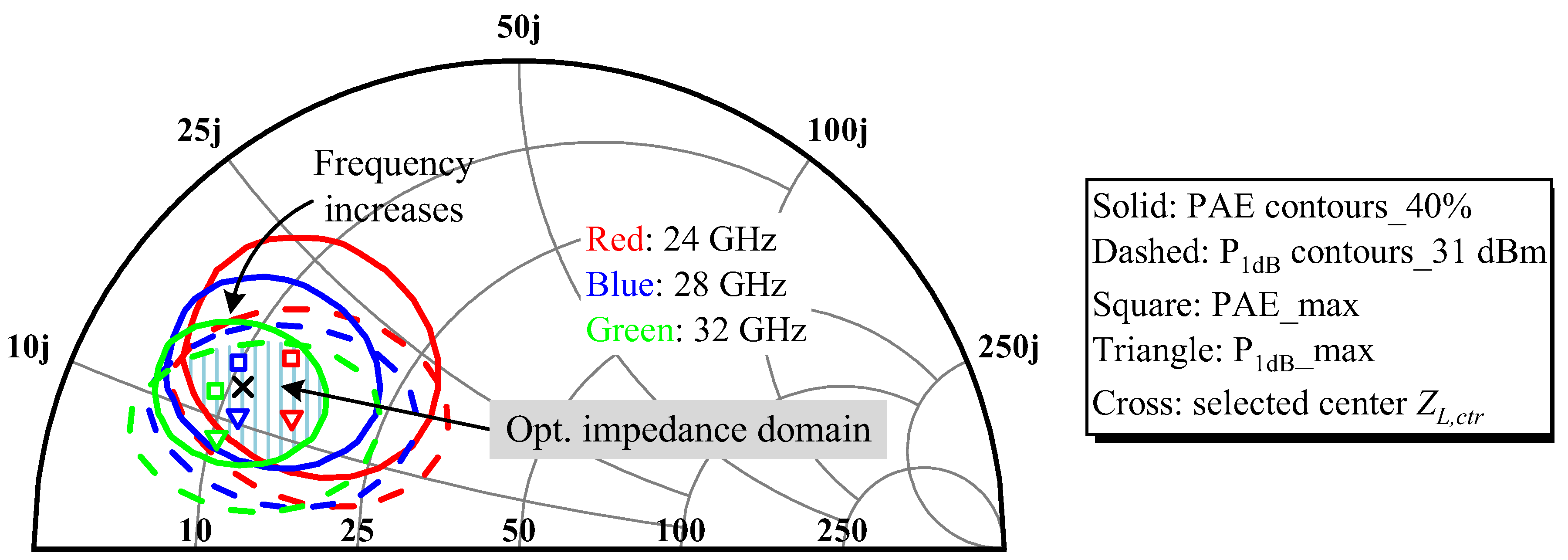
To deal with the shortage of high-frequency output capability induced by the transistor’s gain roll-off and to accommodate the output VSWR, single-tone load-pull procedures were carried out on the stabilized 46 × 8 μm cell at the 1 dB gain compression point (P1dB), the threshold between linear and nonlinear states. Figure 2 plots the generated PAE and P1dB contours of 40% and 31 dBm, respectively, for 24 GHz, 28 GHz, and the extended corner of 32 GHz. The intersection (shaded area) of three groups of contours is the desired optimal impedance domain, whose internal reference matching center ZL,ctr was derived as 11 + j12.9 Ω by conducting a weighted average of impedance values representing the maximum P1dB and PAE at discrete frequencies with emphasis on high-frequency PAE performance. Cout was extracted from load-pull contours as 0.27 pF, and Ropt was selected as 26 Ω according to ZL,ctr [10]. Given the high intrinsic gain and soft compression behavior of GaN-based devices, and to ensure sufficient linear drive power feed, the input stage was likewise compromised under the P1dB condition to identify a Cout of 0.13 pF and an Ropt of 75 Ω for the 46 × 4 μm cell.
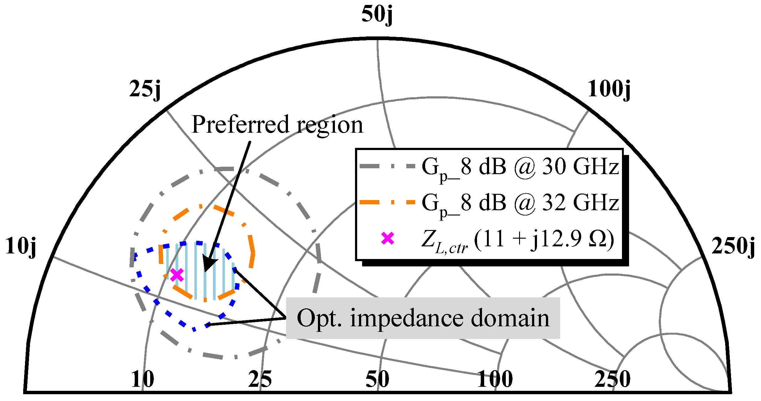
The PA was configured with just one driver stage to reduce the total quiescent current in order to maximize efficiency, yet this also raises the risk of failing to achieve the expected gain, particularly at high frequencies. Hence, adding the 8 dB constant power gain (Gp) concentric circles depicted in Figure 3, where the inner circle at 32 GHz overlaps with the acquired optimal impedance domain, reveals the preferred region that complies with multiple stringent requirements.
3. Design of Broadband Matching Networks
3.1. Discussion of Solutions to Compensate Cout
As the exact item to be matched and the tolerance domain of the impedance trajectory are already clear, the foremost output matching network (OMN) design focuses solely on broadband. As known from the Bode–Fano criterion, the maximum theoretical bandwidth (Δω) that a lossless MN can attain is inversely proportional to the Cout of the established parallel RC-type load. Consequently, how to properly handle Cout and simplify the matching problem into a conventional real impedance transformation (IT) is a viable direction worth investigating. With the purpose of participating in matching, difficulties were encountered after preliminary attempts to utilize the larger Cout in our case by fully integrating it into the MN. An alternative indirect technical route that would allow us to compensate Cout first and match later was promising at this point.
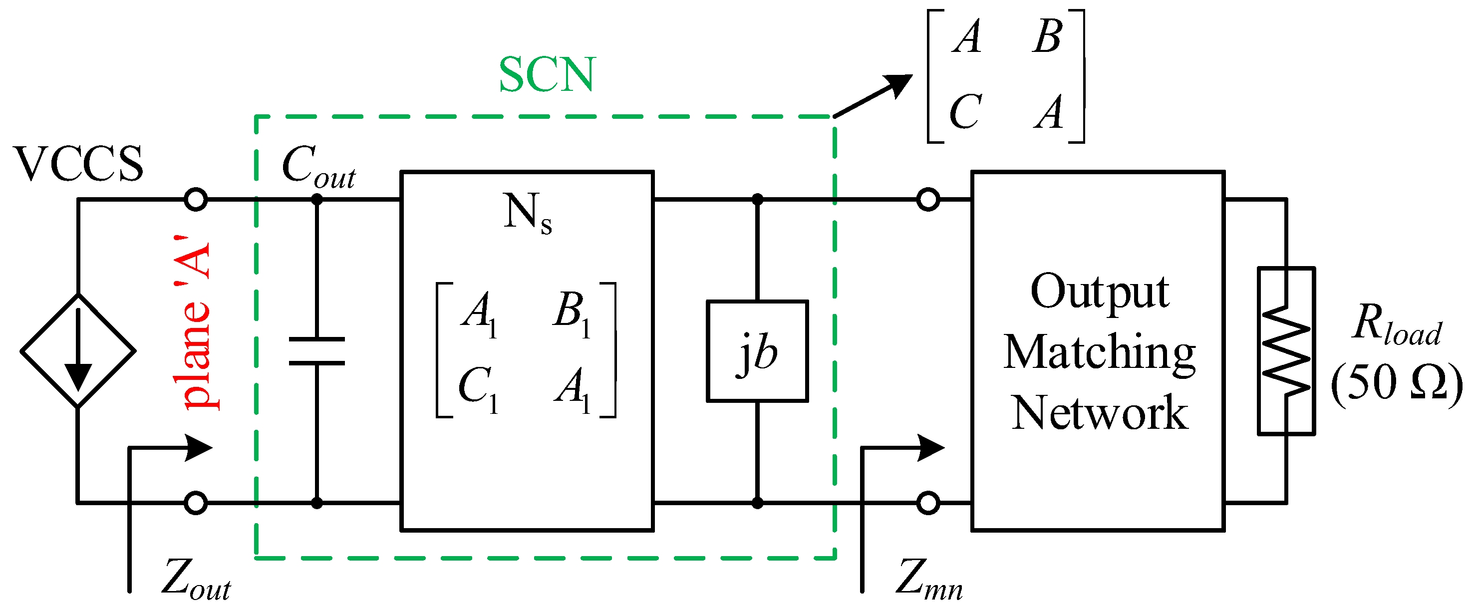
From the perspective of conjugate matching, a symmetrical network with embedded Cout would be a good compensator, as shown in Figure 4, where the custom network Ns is symmetrical, of course, and b is the susceptance of Cout or a commensurate open stub at the operating frequency [22,23]. The transmission matrix components of the symmetrical compensation network (SCN) are defined as A, B, C, and A without subscripts, and those of Ns include the same letters paired with subscript 1. In these conditions, Equation (1) holds. In addition, the output impedance seen by the voltage-controlled current source (VCCS) and the transformation impedance of the OMN are denoted as Zout and Zmn, respectively.
When the interference of Cout is perfectly compensated and presenting the required Ropt to the device, i.e., Zout = Ropt = Zmn, we have
Equation (2) holds upon satisfying B = C = 0 or B = (Ropt)2C. The constraints are further organized according to Equation (1):
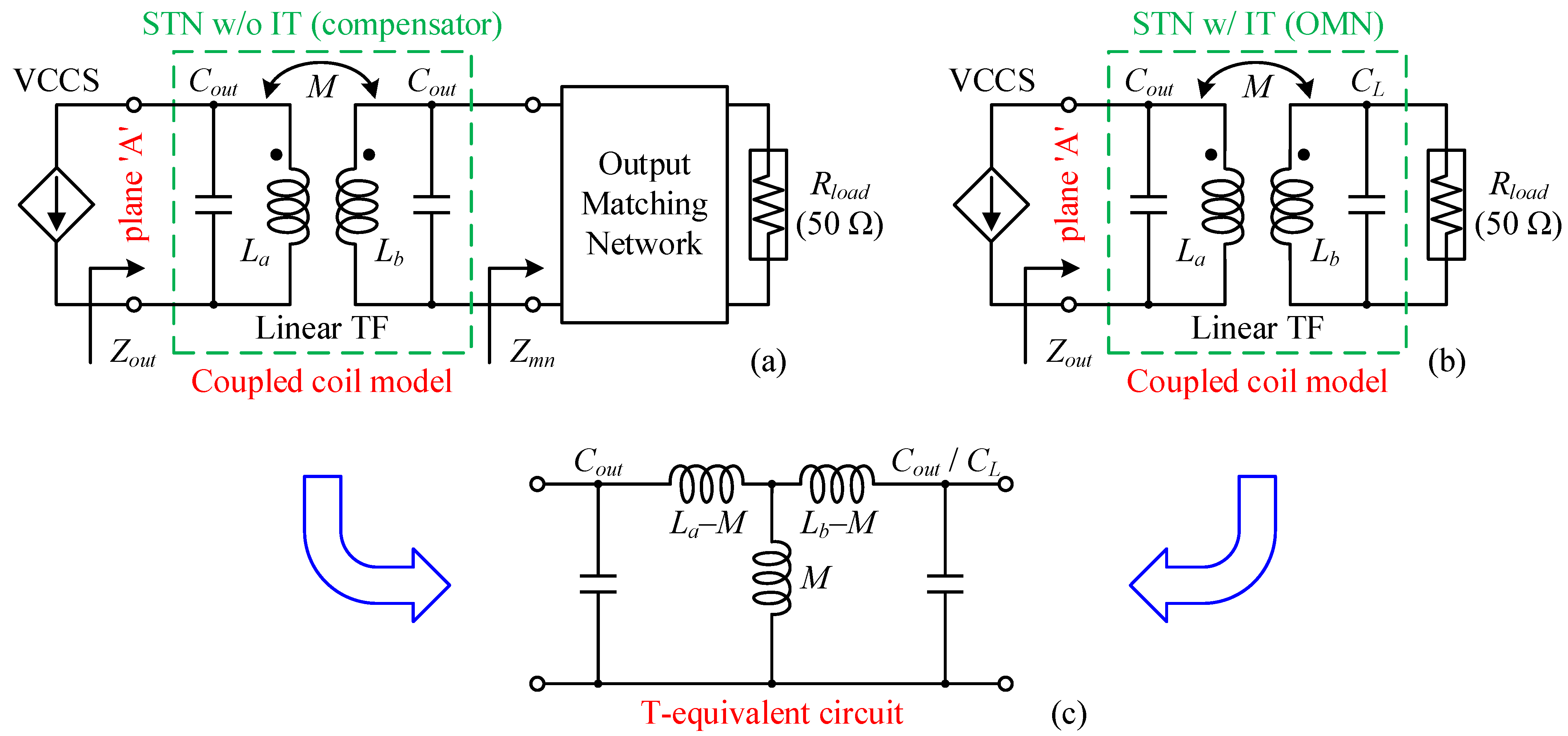
The parameters of different design subjects (Ns), including regular configurations of a single inductor and a transmission line segment, were calculated using Equation (4) with one or more chosen compensation frequencies (fc). Equation (3) determines whether the DC point is also the transmission pole, and if so, SCN has a low-pass (LP) nature. The linear transformer (TF) consisting of two magnetically coupled coils (La and Lb) is considered a special case of Ns when La = Lb, as it can be replaced by an equivalent T-shaped circuit in Figure 5c valid only for AC signals, where the mutual inductance M is determined by the coupling coefficient k, which is expressed as Equation (5) [24]. The synthesized transformer network (STN) formed by a TF without IT function and Cout terminated at its dual ends, as illustrated in Figure 5a, is a kind of compensator whose self-resonant angular frequency (ωres) is written as Equation (6).
Suppose Qr is the reciprocal of the quality factor of the parallel RoptCout at ωres. Following the analytical approach described in [25], while ITR stays in the range restricted by Equation (7), the renewed STN shown in Figure 5b can simultaneously serve as an OMN. However, in practice, a monolithic TF has relatively large loss and area and is frequently employed in CMOS processes with multiple metal layers, whereas the equivalent T network appears easier to implement and offers a high degree of layout freedom.
In conjunction with the present work and the previous discussion, three compensator prototypes covering 22–32 GHz are given in Figure 6a–c, labeled as options A–C, successively, and their frequency responses are displayed in Figure 7. As one may expect, the band-pass (BP) compensator yields three in-band transmission poles with a maximum overhead of six elements to achieve the finest compensation, which is similar to a constant-resistance network. It should be noted that option B was derived from an LP π-type SCN with an fc of 10 GHz by resonating each series and parallel element at the geometric mean frequency (26.5 GHz). Options A and C intuitively seem to have the same implementation complexity, but a closer examination shows that the value of L1 in STN is only 1/2.7 of that in SCN, and L2 can be treated as a drain bias line, indicating that option C prevails in terms of shrinking the layout space. Moreover, MIM capacitors are often sensitive variables in MNs, with minor changes causing large performance discrepancies, making them the subject of electromagnetic (EM) and Monte Carlo analysis. From a process variation and model accuracy point of view, fewer capacitors would be beneficial to improve the chances of success in one trial and for design consistency. On balance, the STN-based compensator wins out of the three options.
For further exploration, the STN with both parasitic compensation and IT features was obtained and is displayed in Figure 6d. The negligible L1 indicates that ITR is close to the limit given in Equation (7). Nevertheless, the existence of L1 is requested for two reasons: (1) a taper that fits with the device drain pin width is needed to reduce step junction discontinuities; (2) a physical connection is needed as a decoupling spacer because the mutual EM effects between the device presented with an established vendor model and microstrip lines used for matching cannot be accounted for during simulations. Therefore, realistic factors will compel the STN acting as an OMN to alter parameters or even topology, leading it to diverge from its original intent. After removing L1, Cout and L2 form a parallel resonant circuit, which triggers thinking about the feasibility of the simplest compensation strategy, i.e., option D, to cancel or lessen the reactance term of the HEMT’s output impedance ZL via resonance. Although only one fc can be specified, it should be enough to yield low-Q impedance Zd within the 6 GHz target bandwidth; hence, a shorted stub TLd was tried to compensate for the effect of Cout, as illustrated in Figure 8. Because of the presence of a small L1 whose total physical length is defined as three times the microstrip line width, option D ought to be called pre-matching. When the length of TLd is tweaked until the resultant output reactance reaches zero at 28 GHz, the real part of Zd increases in the band of interest compared to that of ZL and fluctuates in the narrower range of 14.8–16.5 Ω, allowing a uniform approximation of 16 Ω.
Overall, options C and D are both concise and sensible. The OMNs created based on them in combination with conventional LC ladder LP circuits should have the same topology and similar layout footprint. The latter was simply picked for implementation.
3.2. Synthesis of Two-Section Low-Pass OMN
To begin, there is a non-negligible parasitic capacitance Cpad between the metal plate of the adopted 100 μm square pad and the substrate, which was extracted as Cpad = −1/(ωIm(Z11)) and found to be roughly 21 fF over the target band, where Z11 is the impedance of the pad’s EM model seen from port 1 with port 2 open in the schematic. As each RF pad is directly connected to a 1.8 pF DC-block capacitor, the resulting approximate L-type matching circuit shifts the standard 50 Ω load slightly downward to the capacitive half-plane of the Smith chart; thus, a high-impedance microstrip line was pre-inserted to pull the offset termination back to 48 Ω at 27 GHz center frequency (f0).
A fourth-order Chebyshev LP filter with an FBW of 0.4 was chosen to realize a simple OMN with harmonic suppression for real-to-real transformation from 48 Ω to 16 Ω, where the normalized reactance parameters g were determined from the tabulated data in [11], followed by scaling them to the 50 Ω system and f0 to obtain corresponding inductance and capacitance values [14]. Subsequently, series inductors were swapped with commensurate transmission lines via the single-frequency equivalence technique, and the remaining capacitors in the denormalized network were corrected depending on the computed fringe capacitance [26]. Finally, the ideal network in mixed-element form was turned into layout format using microstrip lines and MIM capacitors from the process design kit (PDK) and attached to the compensation circuit to make up the complete OMN. Repeated iterations of EM simulations and tuning were performed to mitigate the performance deviations caused by element substitution and circuit cascading, and OMN’s frequency response is plotted in Figure 9. The transformed impedance trajectory of 22–32 GHz rotates clockwise tightly around ZL,ctr with increasing frequency and forms a knot. More satisfactorily, it succeeds in nestling overall inside the predefined preferred region. Meanwhile, the second and third harmonic impedances are located in the upper half-plane of the Smith chart and are scattered alongside its margin, implying that the harmonic power dissipation share will be tiny. These encouraging signs give us confidence in the PA’s ability to deliver broadband large-signal output.
3.3. ISMN Developed by Using a Numerical Optimization Method
Due to the device’s non-unilateral operation, input and output impedances will interact. As a result, source-pull simulations for the maximum PAE were re-run on the stabilized 46 × 8 μm cell loaded with the well-developed OMN, and the updated optimal source impedance (ZS,opt) could better represent the current matching requirements. Figure 10 shows that the conjugate of ZS,opt is almost symmetrically distributed in the upper and lower half-planes of the Smith chart along a resistance circle of 4.5 Ω at 23–31 GHz. ZS,opt* can thereby be carefully modeled as a series RLC equivalent circuit, with S-parameter simulations fitting the inductance and capacitance to 110 pH and 0.32 pF, respectively. The obtained RLC network then serves as one end of the interstage matching network (ISMN), with the other side being the driver cell’s output parallel RoptCout model. As such, the ISMN objective is reduced from frequency-varying impedance set transformation to reasonable matching between fixed equivalent circuits.
As the two terms have reactance compositions and ITR is high, ISMN may have to be cascaded with three or more L-sections, resulting in a greater footprint and insertion loss. Under the premise of broadband matching, lower sophistication becomes the main endeavor of ISMN design. If applying the filter synthesis theory, the preferred topology will be a BP structure in order to absorb both parallel Cout and LC series resonance components [12]. Bearing in mind that a BP network doubles the cost of the same order in LP form, a practical ISMN constructed via the analytical method is bound to be bulky for the high ITR case ranging from 4.5 Ω to 75 Ω. Despite having a decent in-band ripple, it is not a design priority. Recall the classic graphical approach of the Smith chart with a constant-Q circle, which only works for broadband transformations between certain impedances and relies on experience to achieve probable compact outcomes. CAD-dependent numerical optimization methods stand out in this context, as they automate the search for the optimal matching topology for arbitrary loads, bandwidth, and complexity demands.
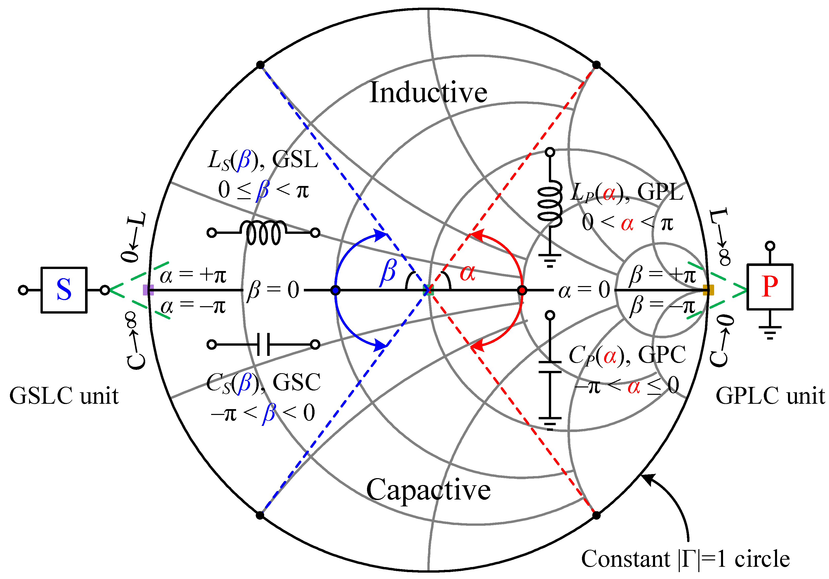
Here, a parametric matching technique based on generalized parallel and series LC units (GPLC and GSLC, respectively) was adopted, and its principle is illustrated in Figure 11 [16]. By characterizing the grounded parallel inductor and capacitor as reactance quantities GPL and GPC and associated with the radian of their reflection coefficients α while the series inductor and capacitor are similarly characterized as reactance quantities GSL and GSC and associated with the radian of their reflection coefficients β, all possible values of inductance and capacitance are mapped to a finite and continuous opening interval (−π, π). This facilitates the rapid automatic adjustment for parameters of GPLC and GSLC units placed together according to predefined matching goals by means of CAD software, thereby arbitrarily altering the network topology while effectively alleviating convergence issues. The inductances LP(α) and LS(β) and capacitances CP(α) and CS(β) are defined as Equations (8)–(11) at the center angular frequency of interest ω0, where Z0 is the normalized impedance (e.g., 50 Ω). In conclusion, the mentioned method is simpler and easier to apply than SRFT and can directly utilize the built-in optimizer of Advanced Design System (ADS), the design platform in which this work was undertaken, without the need to develop separate script code.
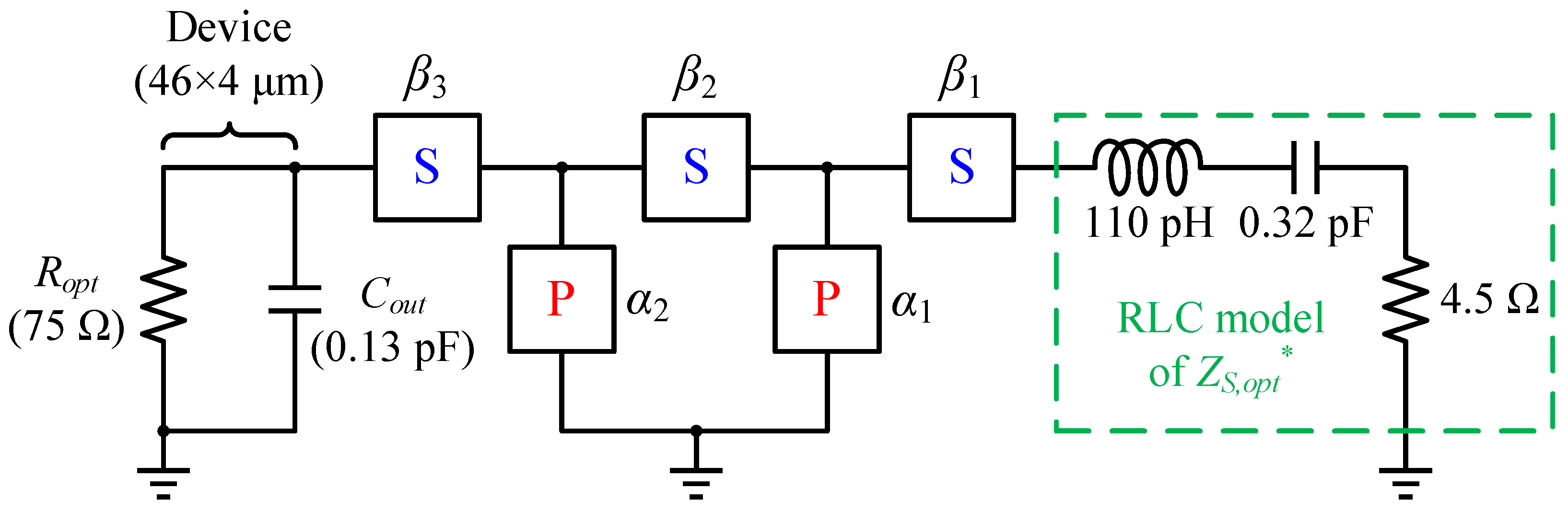
Because the required drive power of the output stage grows with frequency, the high-frequency impedance matching demands special care, and some low-frequency mismatch is deliberately introduced to promote gain flatness. Accordingly, S11 < −15 dB and S21 > −0.2 dB within 23–32 GHz as schematic optimization goals with equal weight were decided. After several trial-and-error attempts, it was found that an ISMN with the five units pictured in Figure 12 was adequate for the task.
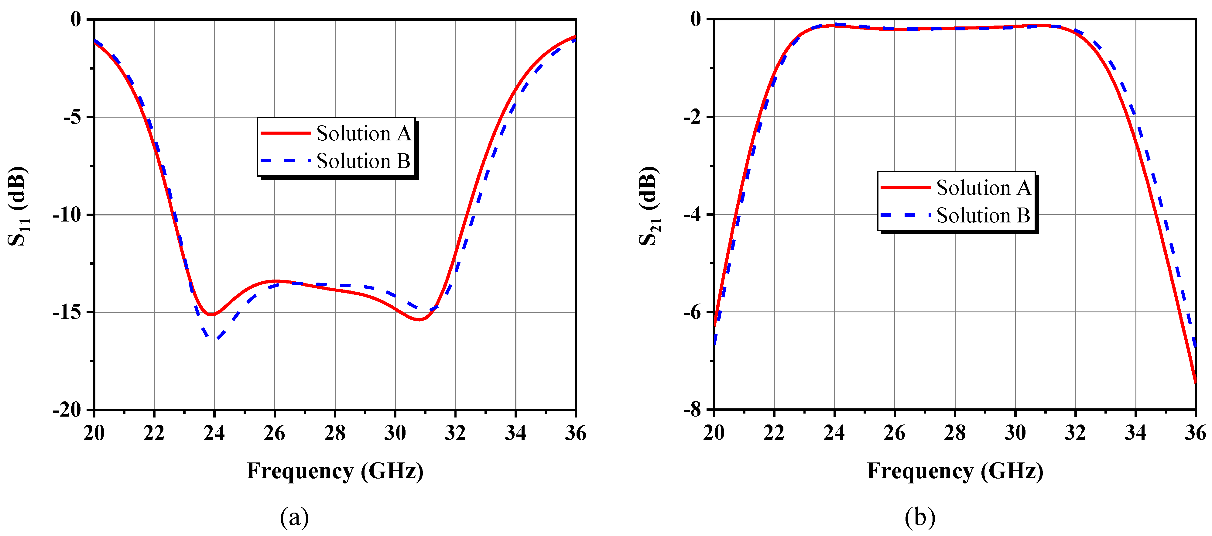
The five radian independent variables involved were assigned random numbers uniformly distributed in the interval (−π, π) generated by MATLAB. If the initialized ISMN happened to produce a good match in the target band, then the gradient-type algorithm procedure was executed using the ADS optimizer; otherwise, automatic optimization was performed in the order of random-before-gradient search. For the sake of avoiding different initial assignment combinations that may affect the final optimization results, these steps were repeated five times to obtain optimal solutions A and B with convergent matching effects, with detailed design parameters listed in Table 1 and frequency responses shown in Figure 13. Because the lumped ISMN corresponding to each solution comprises an indispensable DC-block capacitor and is of comparable complexity, solution A was freely selected to guide the construction of the ISMN’s layout.
3.4. Synthesized IMN in Band-Pass Form
The mission of the input matching network (IMN) is rather straightforward: simply match the observed small-signal input impedance (Zins) of the driver stage to a compensated load of 48 Ω for favorable broadband S11. Zins was captured when the stabilized 46 × 4 μm cell was loaded with a fully built-up post-stage circuit and can be represented in the band as a series RLC form of Zequ. IMN was realized in BP style for the purpose of exploiting the MN’s band selectivity function to suppress out-of-band gain to improve stability while facilitating bandwidth tuning and absorbing the series LC that dominates Zins’s reactance. An analytical method to enlarge the FBW by applying fair mismatch in a manner that compromises the minimum reflection coefficient with regard to the Chebyshev prototype was proposed in [12]. Based on its provided closed-form solutions, the step-by-step IMN design procedure is illustrated in Figure 14.
4. Simulation Results
Figure 15 and Figure 16 depict the schematic and layout of the entire PA. RF and low-frequency bypass capacitors of 0.7 pF and 3 pF were paralleled to the 12 V supply paths of both stages to reduce off-chip parasitic effects and thereby improve the circuit’s stability. For compactness and in consideration of the maximum output current swing to be sustained, narrow microstrip lines of 15 μm and 10 μm width were used for the OMN and rest parts, respectively. Nevertheless, this inevitably increased the ohmic loss of MNs, which in turn damaged efficiency; hence, double-layer metal, as permitted by the process, was intentionally adopted to achieve OMN. Drain bias lines were also thickened with metal to enhance current-carrying capability. All of the passive elements or metal shapes involved in the complete layout were rigorously EM simulated by the 2.5D field simulator (ADS Momentum) in the DC–100 GHz range with a density of 50 mesh cells per wavelength. Afterward, EM/circuit co-simulations were conducted jointly with active device library models, and the suggested PA’s performance in CW mode was thoroughly verified only after full-band unconditional stability was proven.
4.1. Small- and Large-Signal Characterization
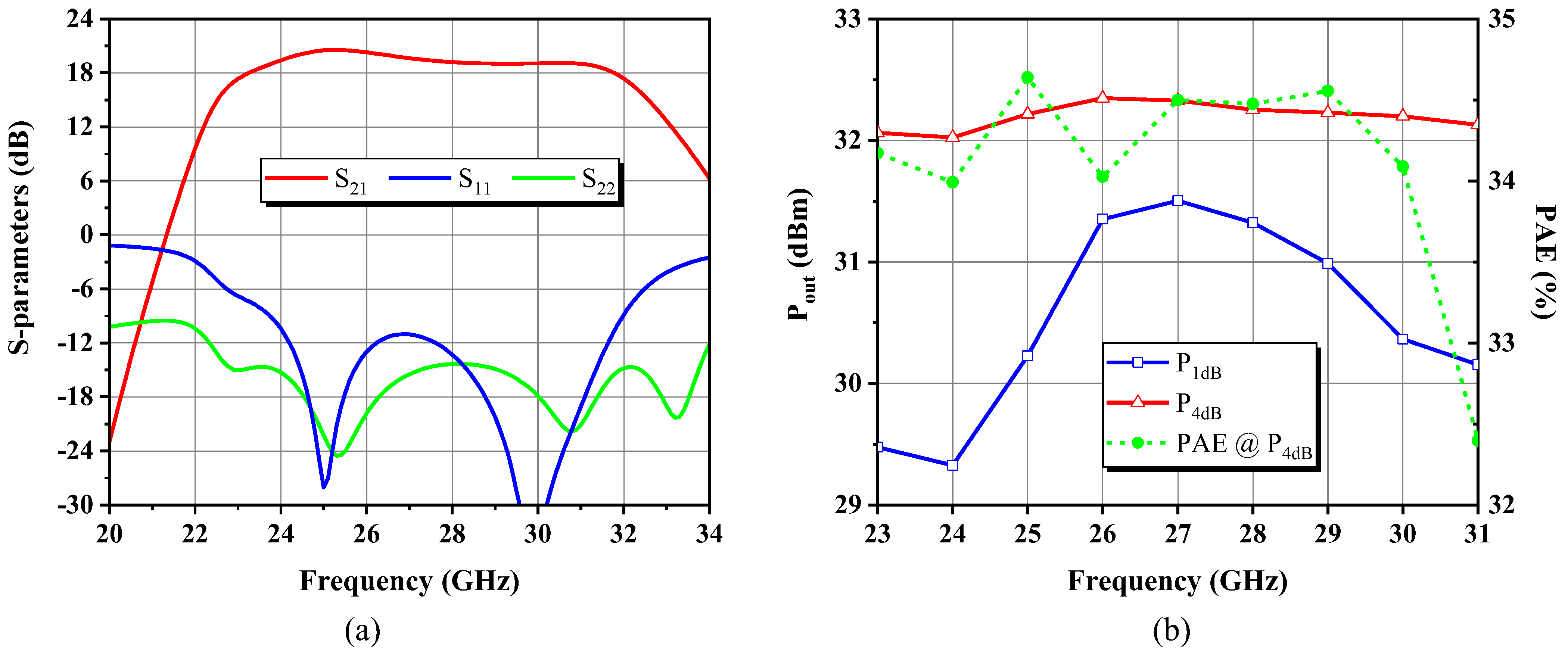
Figure 17a illustrates that S21 was between 19.1 and 20.5 dB within the 24–30 GHz operating bandwidth, with an overall smooth trend except for a small bump near 25.3 GHz. The in-band reflection coefficients S11 and S22 were below −10.4 dB and −14.3 dB, respectively. Although the output stage is power matching by load-pull, the choice of obtaining the equivalent output impedance model at P1dB instead of deep gain compression point, combined with the parasitic compensation network and Chebyshev transformer, eventually resulted in a good S22 value over a wide bandwidth of 23–33 GHz. The loss of RF output signal owing to mismatch is thereby minimized, which improves efficiency to some extent. The harmonic balance findings are given in Figure 17b, where it is shown that P1dB fluctuated more significantly, with a maximum value of 31.5 dBm occurring at f0 and an in-band peak-to-peak difference of 2.2 dB. However, such a difference gradually diminishes with the further boost of Pin to just less than 0.4 dB at 4 dB gain compression, whereas P4dB exceeds 32 dBm with an associated PAE of 34–34.6%, thereby realizing a flat broadband large-signal response.
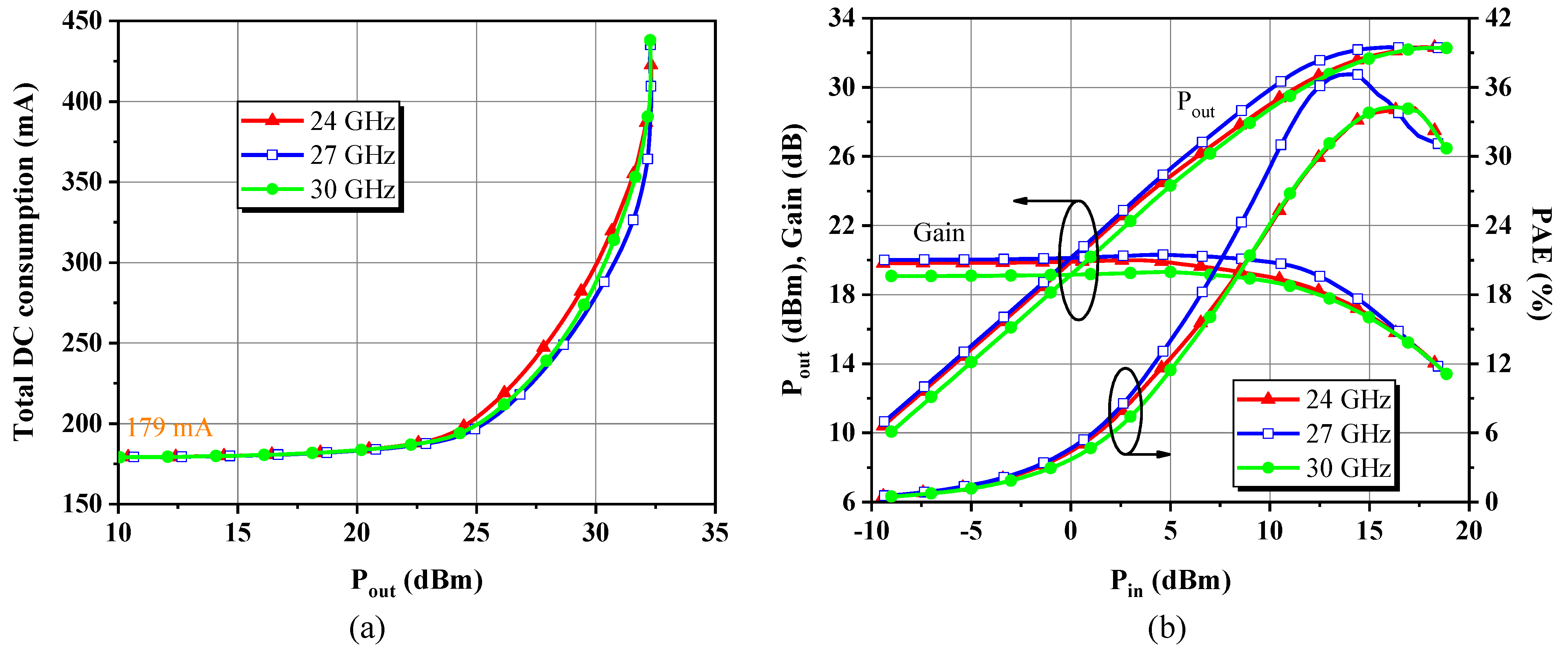
The total current consumption trends and power sweep characteristic curves at low, medium, and high fundamental frequencies are plotted in Figure 18. When driven into saturation with an output of 32.4 dBm, the two-stage PA’s DC consumption grew to a maximum of 423–438 mA and tended to raise the current draw at higher frequencies. The PA operated best at mid-frequency, with a peak PAE of 37.1% at P2dB, corresponding to a Pin of 14 dBm, whereas performance variations at the edge frequencies were similar, with the maximum PAE found in the vicinity of P4dB.
4.2. Electro-Thermal Behavior
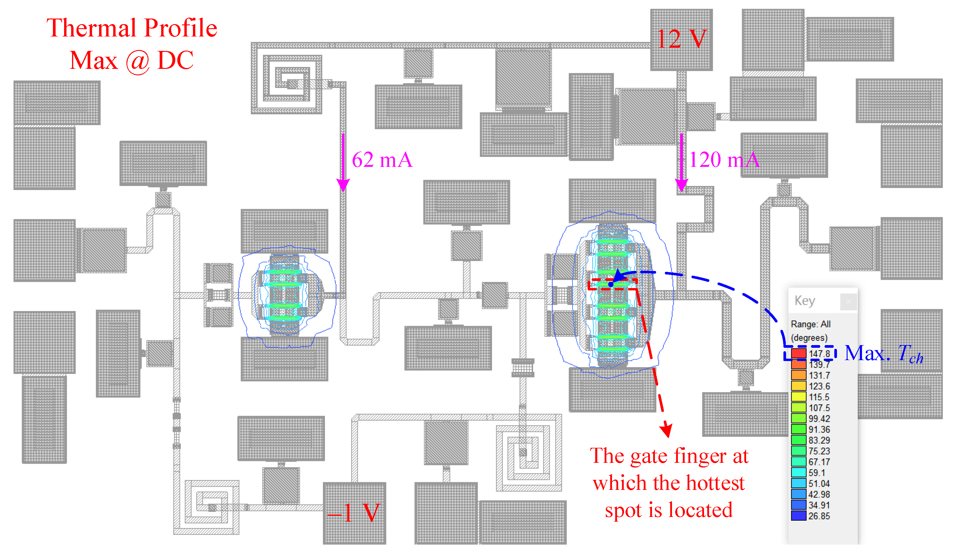
For high-power GaN devices built on a Si substrate with low thermal conductivity, the uneven temperature rise caused by an increasingly severe self-heating effect and thermal coupling between individual gate fingers can degrade the device’s electrical performance or lead to irreversible damage or even burnout. The heat source of an HEMT is concentrated in the channel below the gate, and the related Tch depends not only on the power dissipation, but also on the layout position and nonlinear thermal properties of the substrate material [27]. Therefore, a full 3D thermal-aware analysis for the whole MMIC was performed using the HeatWave Eth Simulator based on the finite-element method (FEM) and built into the Keysight ADS to uncover potential reliability issues and failures.
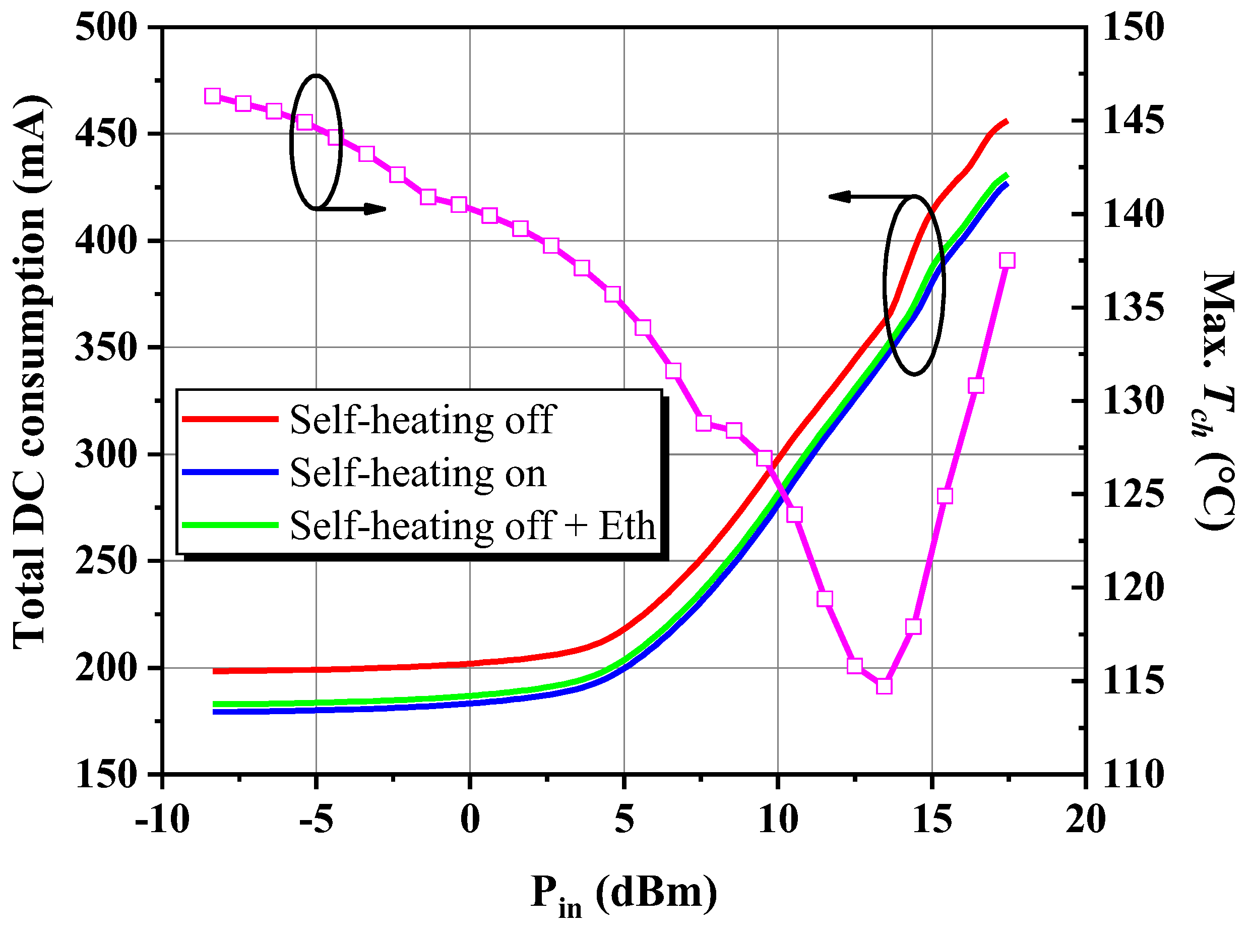
Assuming a fixed base plate temperature (Tbp) of 26.85 °C (300 K), the Joule heat generated from the device’s active region was solely considered to be transferred downward through the 100 μm high-resistivity Si substrate to the bottom, where the heat sink with a constant Tbp is located, while the chip is surrounded by adiabatic surfaces. Figure 19 indicates that the maximum Tch inside the MMIC at a dissipated power density of 4 W/mm under DC circumstances was 147.8 °C, which is denoted as Tch,DC. As expected, the hottest spot lay in the middle gate finger of the critical output-stage transistor. The power-on state without RF signal transmission to the load would be the worst-case scenario for heating, as all of the energy provided was dissipated into heat by the cell, as shown in Figure 20. The maximum Tch variation trend with Pin for the 46 × 8 μm cell at f0 is highly analogous to the corresponding PAE curve in Figure 18b when inverted. Even at the deep gain compression point, the cell drew a large amount of current from the supply, yet the resulting maximum Tch of 137.5 °C was still below Tch,DC, as the PAE remained above 30%. Figure 20 also plots the total DC consumption versus Pin for the two-stage PA when the device model’s self-heating enable switch was on, off, and alternative to performing Eth simulations when it was turned off. The comparison suggests that the static thermal RC network included well-characterized the thermal behavior of the transistor. The reason for the minor deviation of no more than 7 mA in the total current draw predicted with isolated self-heating simulations from the Eth results is that the 1D heat flow model did not and cannot incorporate the positive effect of passive elements adjacent to the HEMT periphery on heat spread. Furthermore, the design manual states that the peak device’s Tch for long-term reliability is 200 °C, and Tch,DC reaches this upper limit when Tbp climbs to 70 °C at the nominal bias point. Nevertheless, for common on-wafer CW testing, the thermal contact of the chip’s backside on the heat sink is poor, which means that Tbp must be kept in a safe range sufficiently below 70 °C to avoid overheating-induced thermal degradation.
The present work occupied an area of only 1.37 mm2, contributing to lower fabrication and production costs. The flatness in gain, Pout, and PAE compare well with previously reported GaN PAs with similar frequency bands across the board in Table 2 with no major fluctuations. Notably, the lowest in-band PAE value was superior and even approached or outperformed the peak PAE of certain comparable designs. In general, the proposed broadband GaN-on-Si PA features are state-of-the-art.
5. Conclusions
Impedance matching is one of the most fundamental and important concepts in MMIC design. The 24–30 GHz GaN PA demonstrated in this paper was developed by alternating the two phases of establishing equivalent matching models and implementing broadband MNs. The realization of broadband response relies on four aspects. First, compact reactive/resistive MNs with frequency-selective characteristics were added, which enhanced the stability of cells while also playing a role in gain equalization. The stagger-tuning technique was then utilized to achieve good high-frequency matching with the introduction of moderate low-frequency mismatch, promoting a flat S21. Second, rather than using a compromise reference impedance as in the conventional scheme, the output parallel RC and input series RLC equivalent circuits were modeled, and the target space consisting of an area and a single point ZL,ctr was determined based on load/source-pull simulations to precisely represent the large-signal matching requirements of the stabilized cell in the broadband, avoiding analytical troubles caused by directly dealing with a series of ZL,opt and ZS,opt at different fundamental frequencies. Third, four possible compensation options were discussed for Cout, a key limiting factor for bandwidth extension. The simplest and most compact of these, a shorted stub with bypass capacitors, was employed to minimize the transistor’s output reactance. Last, according to matching objects and following the principle of miniaturization, an analytical method based on filter synthesis and a numerical optimization method relying on CAD software were flexibly applied to complete the design of these MNs. In particular, a parametric matching technique was adopted for the tricky ISMN design because the numerical optimization method can quickly find the optimal solution among numerous combinations of reactance parameters, thereby striking the right balance between broadband and complexity. The synthesized prototype has a fixed law of increasing and decreasing the number of elements; thus, the analytical method is less cost-effective with high ITR, and both ends of the impedance contain reactance components.
The realized two-stage PA exhibits a balanced P4dB and a high flat associated PAE of over 34% across the band as well as an average linear gain of 19.8 dB with variations of no more than 0.7 dB, confirming the effectiveness of the proposed wideband design strategy. In addition, the maximum Tch projected at a DC dissipated power density of 4 W/mm is 147.8 °C with 300 K back temperature. The present work is the implementation outcome of one of the combinations of several solutions explored, which can be adapted to specific 5G mmW applications such as integration into T/R-module front ends or as driver amplifiers to better meet the needs in terms of layout, dimensions, and broadband performance.
Author Contributions
Conceptualization, L.P.; methodology, L.P.; software, L.P.; validation, L.P.; formal analysis, L.P.; investigation, L.P.; data curation, L.P.; writing—original draft preparation, L.P.; writing—review and editing, L.P. and Z.Z.; visualization, L.P.; supervision, G.Z.; project administration, Z.Z. and G.Z.; funding acquisition, G.Z. All authors have read and agreed to the published version of the manuscript.
Funding
This research was funded by the National Key R&D Program of China, grant number 2018YFB1802100, and the National Natural Science Foundation of China, grant number 61974035.
Institutional Review Board Statement
Not applicable.
Informed Consent Statement
Not applicable.
Data Availability Statement
Not applicable.
Conflicts of Interest
The authors declare no conflict of interest.
Nomenclature
| 2D | Two-dimensional |
| 3D | Three-dimensional |
| 3GPP | 3rd generation partnership project |
| 5G | Fifth-generation cellular network |
| AC | Alternating current |
| ADS | Advanced design system |
| BP | Band-pass |
| CAD | Computer-aided design |
| CMOS | Complementary metal-oxide semiconductor |
| CW | Continuous-wave |
| DC | Direct current |
| EM | Electromagnetic |
| Eth | Electro-thermal |
| FBW | Fractional bandwidth |
| FEM | Finite-element method |
| FR | Frequency range |
| GaN-on-Si | Gallium nitride-on-silicon |
| GPLC | Generalized parallel LC |
| GSLC | Generalized series LC |
| HEMT | High-electron-mobility transistor |
| IMN | Input matching network |
| ISMN | Interstage matching network |
| IT | Impedance transformation |
| ITR | Impedance transformation ratio |
| LP | Low-pass |
| MIM | Metal-insulator-metal |
| MMIC | Monolithic microwave integrated circuit |
| mmW | Millimeter-wave |
| MN | Matching network |
| NR | New radio |
| OMN | Output matching network |
| PA | Power amplifier |
| PAE | Power-added efficiency |
| PDK | Process design kit |
| RF | Radio frequency |
| SCN | Symmetrical compensation network |
| SRFT | Simplified real-frequency technique |
| STN | Synthesized transformer network |
| TF | Transformer |
| VCCS | Voltage-controlled current source |
| VSWR | Voltage standing wave ratio |
References
- Nakatani, K.; Yamaguchi, Y.; Hangai, M.; Shinjo, S. A Ka-band CW 15.5 W 15.6% fractional bandwidth GaN power amplifier MMIC using wideband BPF inter-stage matching network. In Proceedings of the 2019 IEEE BiCMOS and Compound Semiconductor Integrated Circuits and Technology Symposium (BCICTS), IEEE, Nashville, TN, USA, 3–6 November 2019; pp. 1–4. [Google Scholar]
- Neininger, P.; John, L.; Brückner, P.; Friesicke, C.; Quay, R.; Zwick, T. Design, analysis and evaluation of a broadband high-power amplifier for Ka-band frequencies. In Proceedings of the 2019 IEEE MTT-S International Microwave Symposium (IMS), IEEE, Boston, MA, USA, 2–7 June 2019; pp. 564–567. [Google Scholar]
- Chen, S.; Nayak, S.; Campbell, C.; Reese, E. High efficiency 5W/10W 32–38GHz power amplifier MMICs utilizing advanced 0.15 µm GaN HEMT technology. In Proceedings of the 2016 IEEE Compound Semiconductor Integrated Circuit Symposium (CSICS), IEEE, Austin, TX, USA, 23–26 October 2016; pp. 1–4. [Google Scholar]
- Alizadeh, A.; Frounchi, M.; Medi, A. On design of wideband compact-size Ka/Q-band high-power amplifiers. IEEE Trans. Microw. Theory Tech. 2016, 64, 1831–1842. [Google Scholar] [CrossRef]
- Shin, D.H.; Yom, I.B.; Kim, D.W. 6-GHz-to-18-GHz AlGaN/GaN Cascaded Nonuniform Distributed Power Amplifier MMIC Using Load Modulation of Increased Series Gate Capacitance. ETRI J. 2017, 39, 737–745. [Google Scholar] [CrossRef]
- Kerherve, E.; Demirel, N.; Ghiotto, A.; Larie, A.; Deltimple, N.; Pham, J.-M.; Mancuso, Y.; Garrec, P. A broadband 4.5–15.5-GHz SiGe power amplifier with 25.5-dBm peak saturated output power and 28.7% maximum PAE. IEEE Trans. Microw. Theory Tech. 2015, 63, 1621–1632. [Google Scholar] [CrossRef]
- Lee, H.; Lee, W.; Kim, T.; Helaoui, M.; Ghannouchi, F.M.; Yang, Y. 6–18 GHz GaAs pHEMT broadband power amplifier based on dual-frequency selective impedance matching technique. IEEE Access 2019, 7, 66275–66280. [Google Scholar] [CrossRef]
- Peng, L.; Chen, J.; Zhang, Z.; Huang, Y.; Wang, T.; Zhang, G. Design of broadband high-gain GaN MMIC power amplifier based on reactive/resistive matching and feedback technique. IEICE Electron. Express 2021, 18, 20210313. [Google Scholar] [CrossRef]
- Bahl, I. Fundamentals of RF and Microwave Transistor Amplifiers; John Wiley & Sons: Hoboken, NJ, USA, 2009. [Google Scholar]
- Peng, L.; Chen, J.; Zhang, Z.; Zhang, G. Design of an Efficient 24–30 GHz GaN MMIC Power Amplifier Using Filter-Based Matching Networks. Electronics 2022, 11, 1934. [Google Scholar] [CrossRef]
- Matthaei, G.L. Tables of Chebyshev impedance–transforming networks of low-pass filter form. Proc. IEEE 1964, 52, 939–963. [Google Scholar] [CrossRef] [Green Version]
- Dawson, D.E. Closed-form solutions for the design of optimum matching networks. IEEE Trans. Microw. Theory Tech. 2008, 57, 121–129. [Google Scholar] [CrossRef]
- Meng, X.; Yu, C.; Liu, Y.; Wu, Y. Design approach for implementation of class-J broadband power amplifiers using synthesized band-pass and low-pass matching topology. IEEE Trans. Microw. Theory Tech. 2017, 65, 4984–4996. [Google Scholar] [CrossRef]
- Chen, K.; Peroulis, D. Design of highly efficient broadband class-E power amplifier using synthesized low-pass matching networks. IEEE Trans. Microw. Theory Tech. 2011, 59, 3162–3173. [Google Scholar] [CrossRef]
- Yang, M.; Xia, J.; Guo, Y.; Zhu, A. Highly efficient broadband continuous inverse class-F power amplifier design using modified elliptic low-pass filtering matching network. IEEE Trans. Microw. Theory Tech. 2016, 64, 1515–1525. [Google Scholar] [CrossRef] [Green Version]
- Meghdadi, M.; Medi, A. Design of 6–18-GHz high-power amplifier in GaAs pHEMT technology. IEEE Trans. Microw. Theory Tech. 2017, 65, 2353–2360. [Google Scholar] [CrossRef]
- Yarman, B.S.; Carlin, H.J. A simplified “real frequency” technique applied to broad-band multistage microwave amplifiers. IEEE Trans. Microw. Theory Tech. 1982, 30, 2216–2222. [Google Scholar] [CrossRef]
- Kumar, A.; Moradpour, M.; Losito, M.; Franke, W.T.; Ramasamy, S.; Baccoli, R.; Gatto, G. Wide band gap devices and their application in power electronics. Energies 2022, 15, 9172. [Google Scholar] [CrossRef]
- Prado, E.O.; Bolsi, P.C.; Sartori, H.C.; Pinheiro, J.R. An overview about Si, Superjunction, SiC and GaN power MOSFET technologies in power electronics applications. Energies 2022, 15, 5244. [Google Scholar] [CrossRef]
- Colantonio, P.; Giofrè, R. A GaN-on-Si MMIC power amplifier with 10 W output power and 35% efficiency for Ka-Band satellite downlink. In Proceedings of the 2020 15th European Microwave Integrated Circuits Conference (EuMIC), IEEE, Utrecht, The Netherlands, 10–15 January 2021; pp. 29–32. [Google Scholar]
- Tong, X.; Zhang, S.; Zheng, P.; Xu, J.; Wang, R. 23.5–30 GHz gallium nitride on silicon power amplifier MMIC with 7.6–12.4 W saturation output power. Microw. Opt. Technol. Lett. 2019, 61, 1797–1801. [Google Scholar] [CrossRef]
- Ardekani, M.H.M.; Abiri, H. A new approach to design wide band power amplifiers by compensating parasitic elements of transistors. AEU-Int. J. Electron. Commun. 2018, 92, 1–7. [Google Scholar] [CrossRef]
- Rubio, J.J.M.; Quaglia, R.; Piacibello, A.; Camarchia, V.; Tasker, P.J.; Cripps, S. 3–20-GHz GaN MMIC Power Amplifier Design Through a COUT Compensation Strategy. IEEE Microw. Wirel. Compon. Lett. 2021, 31, 469–472. [Google Scholar] [CrossRef]
- Huang, P.C.; Tsai, Z.M.; Lin, K.Y.; Wang, H. A 17–35 GHz broadband, high efficiency PHEMT power amplifier using synthesized transformer matching technique. IEEE Trans. Microw. Theory Tech. 2011, 60, 112–119. [Google Scholar] [CrossRef]
- Chen, Y.; Wu, Y.; Luo, L.; Wang, Q.; Zhang, Y.; Yan, B.; Xu, R.; Xu, Y. Design of 18–40 GHz GaN reactive matching power amplifiers using one-order and two-order synthesised transformer networks. IET Microw. Antennas Propag. 2022, 16, 78–90. [Google Scholar] [CrossRef]
- Yarman, B.S.; Aksen, A. An integrated design tool to construct lossless matching networks with mixed lumped and distributed elements. IEEE Trans. Circuits Syst. I Fundam. Theory Appl. 1992, 39, 713–723. [Google Scholar] [CrossRef]
- Ramella, C.; Pirola, M.; Reale, A.; Ramundo, M.; Colantonio, P.; Der Maur, M.A.; Camarchia, V.; Piacibello, A.; Giofrè, R. Thermal-aware GaN/Si MMIC design for space applications. In Proceedings of the 2019 IEEE International Conference on Microwaves, Antennas, Communications and Electronic Systems (COMCAS), IEEE, Tel-Aviv, Israel, 4–6 November 2019; pp. 1–6. [Google Scholar]
- Qorvo. High Frequency Amplifiers, TGA2594 Data Sheet. Available online: http://www.qorvo.com (accessed on 11 November 2022).
Figure 1.
Simplified equivalent circuit model of an HEMT.

Figure 2.
Simulated load-pull contours at P1dB for the output stage cell.

Figure 3.
Preferred region in the optimal impedance domain.

Figure 4.
Output circuit composed of SCN and OMN.

Figure 5.
STNs (a) without and (b) with IT function and (c) their AC-equivalent circuits.

Figure 6.
(a) LP compensator with Ns of T-type LCL topology. (b) BP compensator converted from an LP SCN with three lumped elements. (c) STN as a compensator only. (d) STN capable of realizing the transformation from Rload to Ropt.
Figure 6.
(a) LP compensator with Ns of T-type LCL topology. (b) BP compensator converted from an LP SCN with three lumped elements. (c) STN as a compensator only. (d) STN capable of realizing the transformation from Rload to Ropt.

Figure 7.
Ideal frequency responses of compensators: (a) S11; (b) S21.

Figure 8.
Illustration and results of reactance compensation for the output impedance of a 46 × 8 μm power cell using a shorted stub.
Figure 8.
Illustration and results of reactance compensation for the output impedance of a 46 × 8 μm power cell using a shorted stub.

Figure 9.
EM-simulated transformation feature (S11) of OMN from 22 to 90 GHz.

Figure 10.
Impedance distribution of ZS,opt* and its series RLC equivalent circuit.

Figure 11.
GPLC and GSLC reactance matching units.

Figure 12.
ISMN represented by GPLC and GSLC units.

Figure 13.
Ideal frequency response of ISMN in solution A and B cases: (a) S11; (b) S21.

Figure 14.
IMN design flow: (a) LP prototype after impedance and frequency scaling; (b) converted BP version; (c) upward IT of Rload to 48 Ω; (d) Norton transformation to remove the ideal transformer; (e) network optimization for realistic Zins; (f) corresponding ultimate IMN in mixed-element form.
Figure 14.
IMN design flow: (a) LP prototype after impedance and frequency scaling; (b) converted BP version; (c) upward IT of Rload to 48 Ω; (d) Norton transformation to remove the ideal transformer; (e) network optimization for realistic Zins; (f) corresponding ultimate IMN in mixed-element form.

Figure 15.
Schematic diagram of the two-stage PA.

Figure 16.
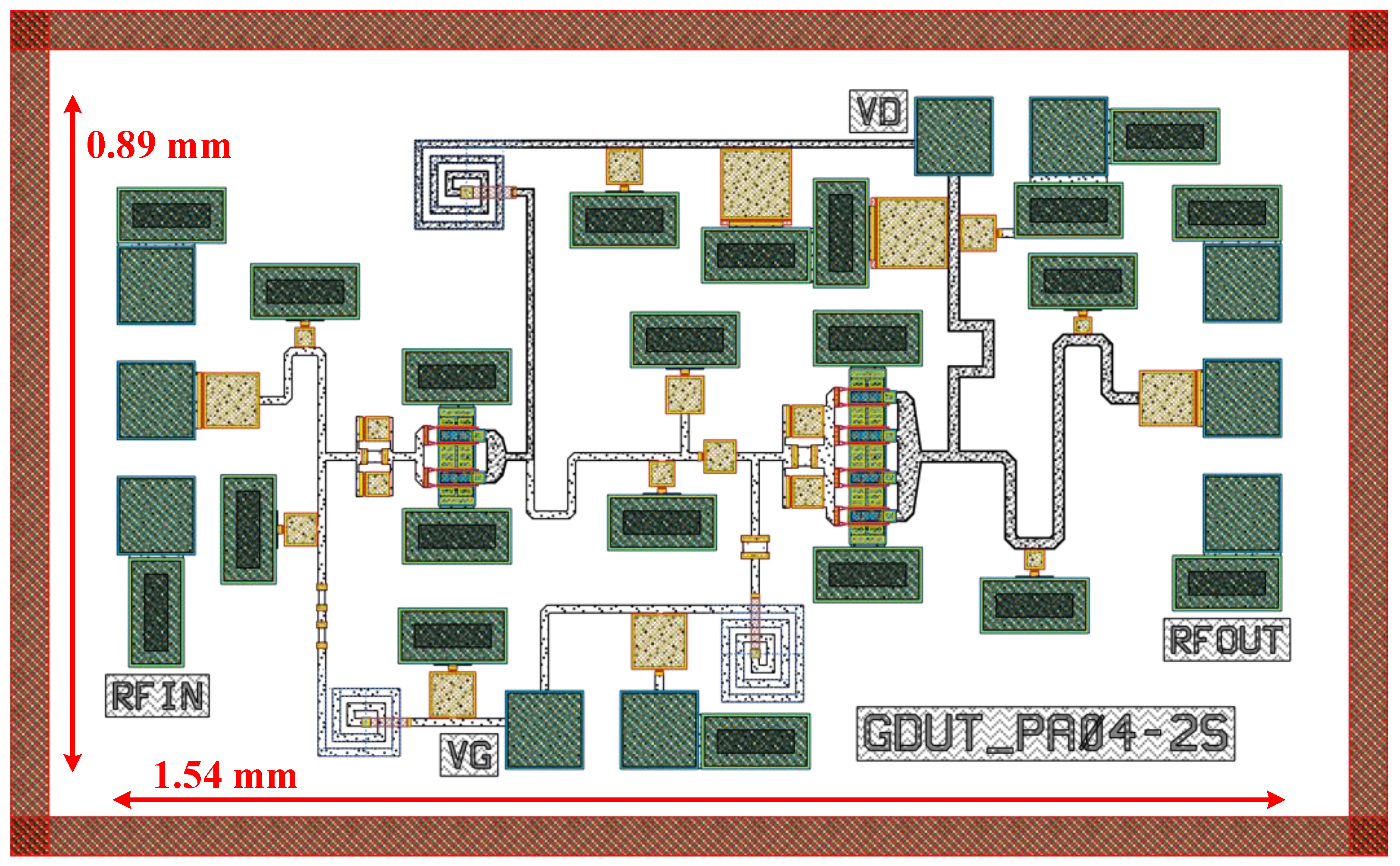
Complete layout of the 24–30 GHz GaN MMIC PA, chip size (including dicing streets): 1.8 × 1.1 mm2.
Figure 16.
Complete layout of the 24–30 GHz GaN MMIC PA, chip size (including dicing streets): 1.8 × 1.1 mm2.

Figure 17.
Simulated (a) S-parameters, (b) Pout, and PAE at 4 dB gain compression.

Figure 18.
Simulated (a) total DC consumption versus Pout, (b) Pout, PAE, and gain behaviors with respect to Pin at three discrete frequencies.
Figure 18.
Simulated (a) total DC consumption versus Pout, (b) Pout, PAE, and gain behaviors with respect to Pin at three discrete frequencies.

Figure 19.
Two-dimensional (2D) thermal map of the designed MMIC at a backside temperature of 26.85 °C obtained from ADS HeatWave.
Figure 19.
Two-dimensional (2D) thermal map of the designed MMIC at a backside temperature of 26.85 °C obtained from ADS HeatWave.

Figure 20.
Total DC consumption and steady-state maximum channel temperature within the chip evaluated for different Pin at f0.
Figure 20.
Total DC consumption and steady-state maximum channel temperature within the chip evaluated for different Pin at f0.


Table 1.
Design parameters for ISMN at f0.
| Solution | β1 | α1 | β2 | α2 | β3 |
|---|---|---|---|---|---|
| A | −0.065 | 3 | 0.107 | −2.912 | 1.31 |
| 3.63 pF | 21 pH | 16 pH | 1.02 pF | 226 pH | |
| B | 0.048 | −3.011 | −0.098 | 2.898 | 1.295 |
| 7 pH | 1.8 pF | 2.4 pF | 36 pH | 223 pH |
Table 2.
Performance summary and comparisons with contemporary work.
| Ref. | [2] | [3] | [8] | [10] | [21] | TGA2594 [28] | This Work |
|---|---|---|---|---|---|---|---|
| Process | 0.1 μm GaN/SiC | 0.15 μm GaN/SiC | 0.1 μm GaN/Si | 0.1 μm GaN/Si | 0.1 μm GaN/Si | 0.15 μm GaN/SiC | 0.1 μm GaN/Si |
| VD (V) | 15 | 20 | 12 | 12 | 12 | 20 | 12 |
| Meas. mode | Pulsed | CW | Pulsed | Pulsed | Pulsed | CW | CW |
| Freq. (GHz) (FBW) | 27–34 (23%) | 32–38 (17.1%) | 22–27 (20.4%) | 24–30 (22.2%) | 24–30 (22.2%) | 27–31 (13.8%) | 24–30 (22.2%) |
| Gain (dB) | 20.5 ± 1.5 | 17 ± 0.5 | 24 ± 0.5 | 29 ± 0.4 | 17.9 ± 1.5 | 23.6 ± 1.9 | 19.8 ± 0.7 |
| Pout (dBm) | 38.7 ± 0.4 | 36.7 ± 0.5 | 31 ± 0.7 | 30.7 ± 0.2 | 39.9 ± 1 | 37 ± 0.4 | 32.2 ± 0.2 |
| PAE (%) | 24.5–30.5 a | 25–34 c | 30.5–36.9 b | 30.6–34.7 a | 24–37 b | 26.5–30.3 c | 34–34.6 a |
| Size (mm2) | 4.5 × 3.5 | 2.22 × 1.6 | 1.8 × 0.87 | 1.94 × 0.83 | 3.7 × 3.2 | 3.24 × 1.74 | 1.54 × 0.89 |
a PAE at specific gain compression point. b PAE at saturated output power. c PAE at specific input drive.
Disclaimer/Publisher’s Note: The statements, opinions and data contained in all publications are solely those of the individual author(s) and contributor(s) and not of MDPI and/or the editor(s). MDPI and/or the editor(s) disclaim responsibility for any injury to people or property resulting from any ideas, methods, instructions or products referred to in the content. |
© 2023 by the authors. Licensee MDPI, Basel, Switzerland. This article is an open access article distributed under the terms and conditions of the Creative Commons Attribution (CC BY) license (https://creativecommons.org/licenses/by/4.0/).
Share and Cite
MDPI and ACS Style
Peng, L.; Zhang, Z.; Zhang, G. Efficient GaN-on-Si Power Amplifier Design Using Analytical and Numerical Optimization Methods for 24–30 GHz 5G Applications. Electronics 2023, 12, 1750. https://doi.org/10.3390/electronics12071750
AMA Style
Peng L, Zhang Z, Zhang G. Efficient GaN-on-Si Power Amplifier Design Using Analytical and Numerical Optimization Methods for 24–30 GHz 5G Applications. Electronics. 2023; 12(7):1750. https://doi.org/10.3390/electronics12071750
Chicago/Turabian StylePeng, Lin, Zhihao Zhang, and Gary Zhang. 2023. "Efficient GaN-on-Si Power Amplifier Design Using Analytical and Numerical Optimization Methods for 24–30 GHz 5G Applications" Electronics 12, no. 7: 1750. https://doi.org/10.3390/electronics12071750
Note that from the first issue of 2016, this journal uses article numbers instead of page numbers. See further details here.