9.9 µW, 140 dB DR, and 93.27 dB SNDR, Double Sampling ΔΣ Modulator Using High Swing Inverter-Based Amplifier for Digital Hearing Aids

Abstract
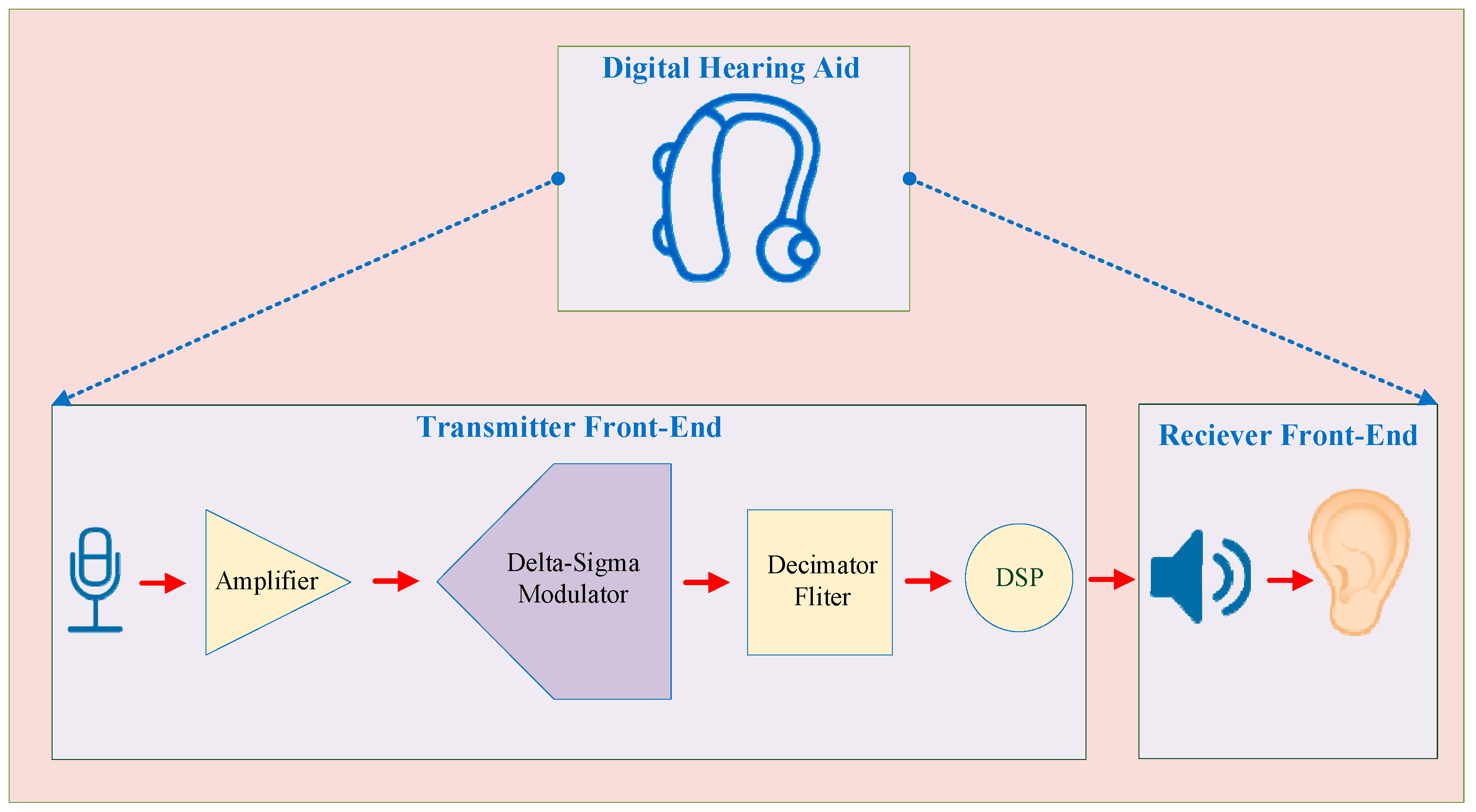
:1. Introduction
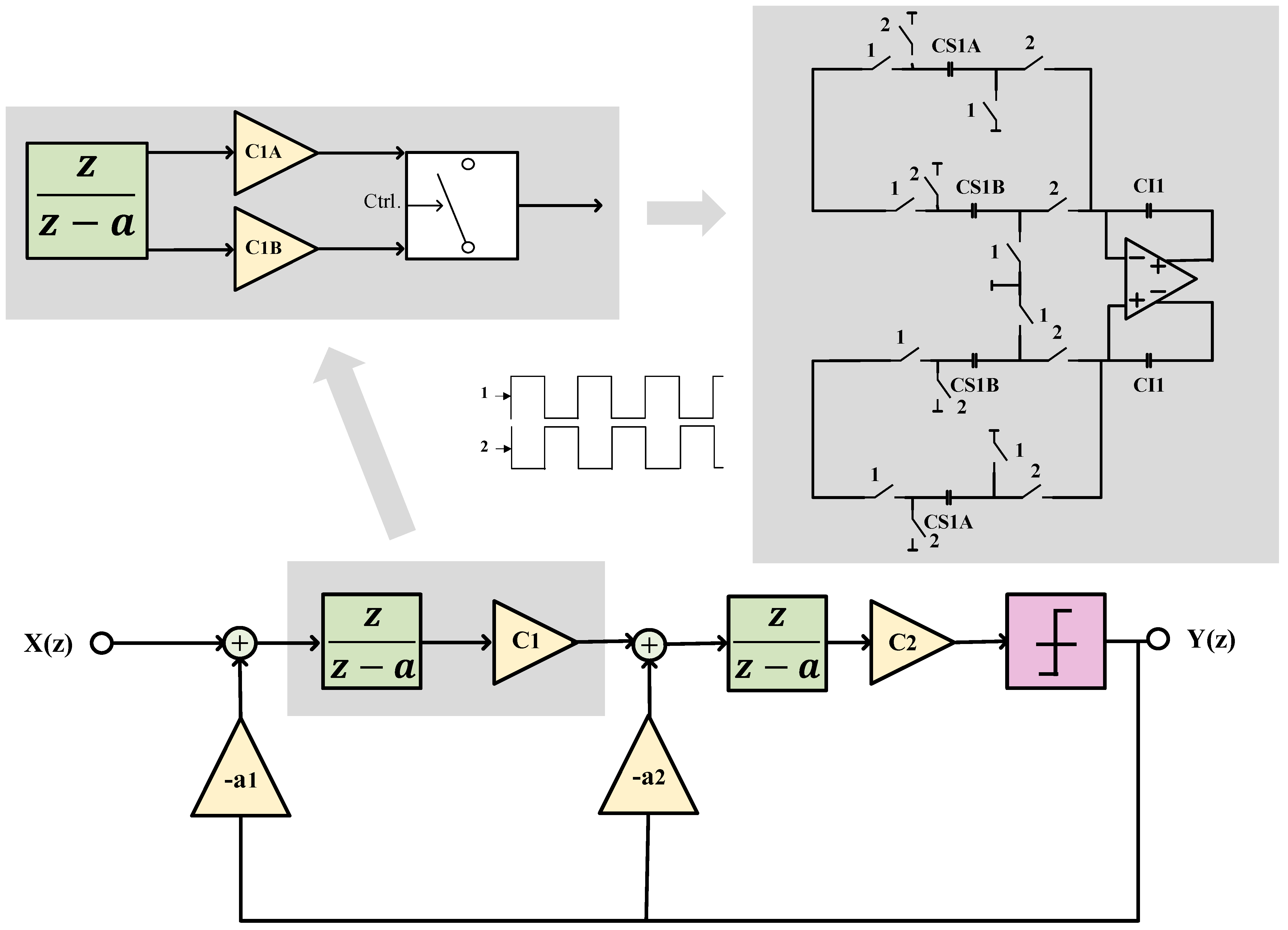
2. System-Level Design of the Proposed ΔΣ Modulator
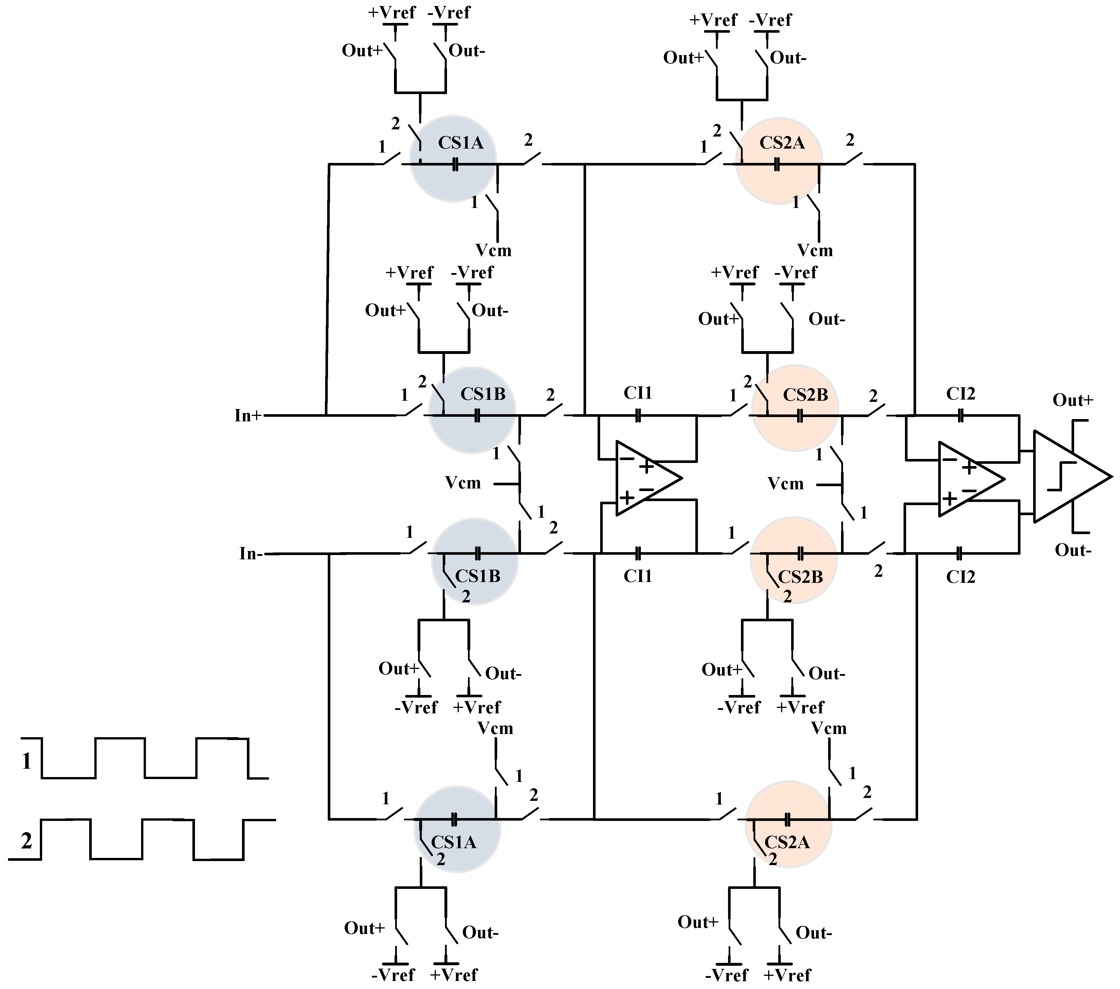
3. Circuit Implementation of the Proposed ΔΣ Modulator
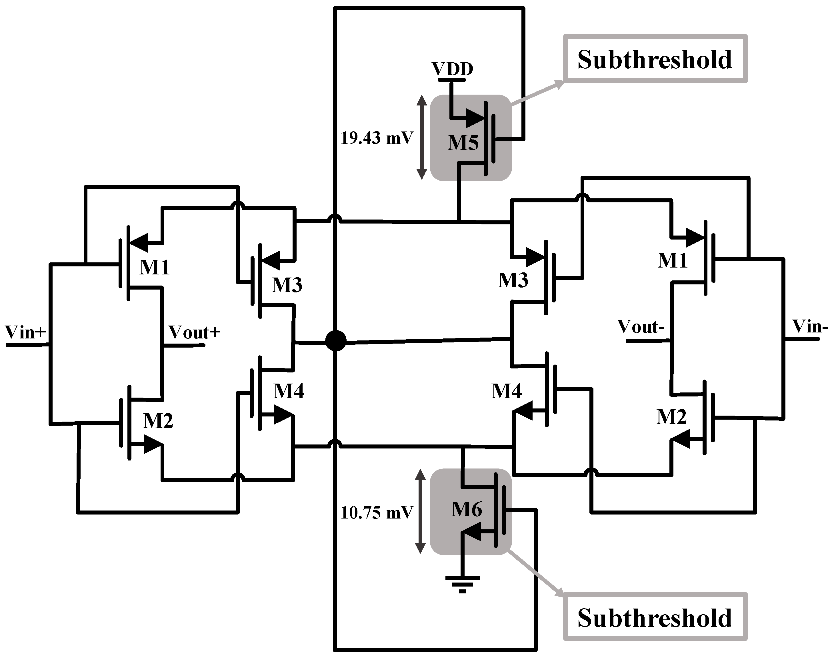
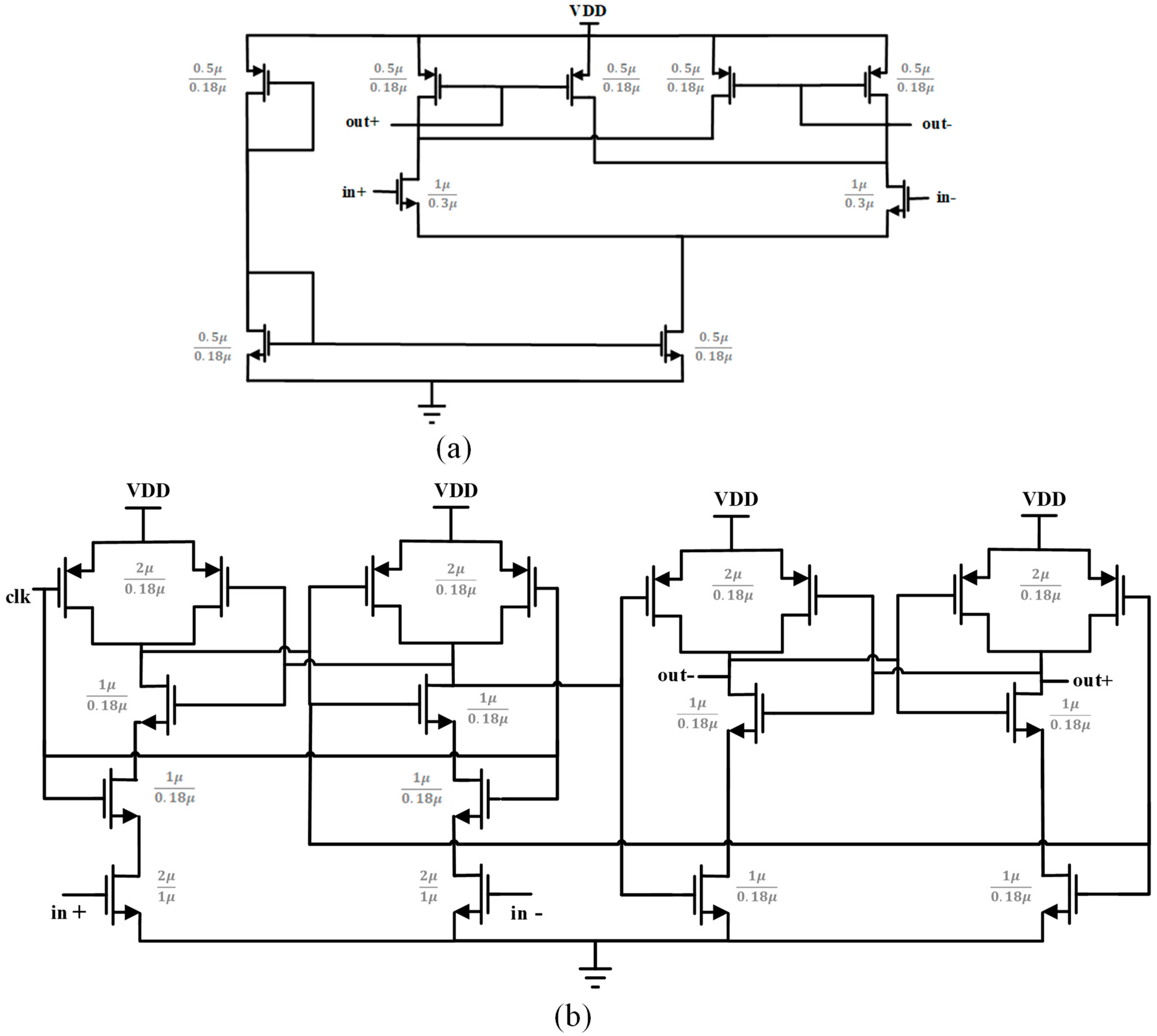
3.1. The Proposed Self-Biased Differential Inverter-Based Amplifier with Swing Enhancement
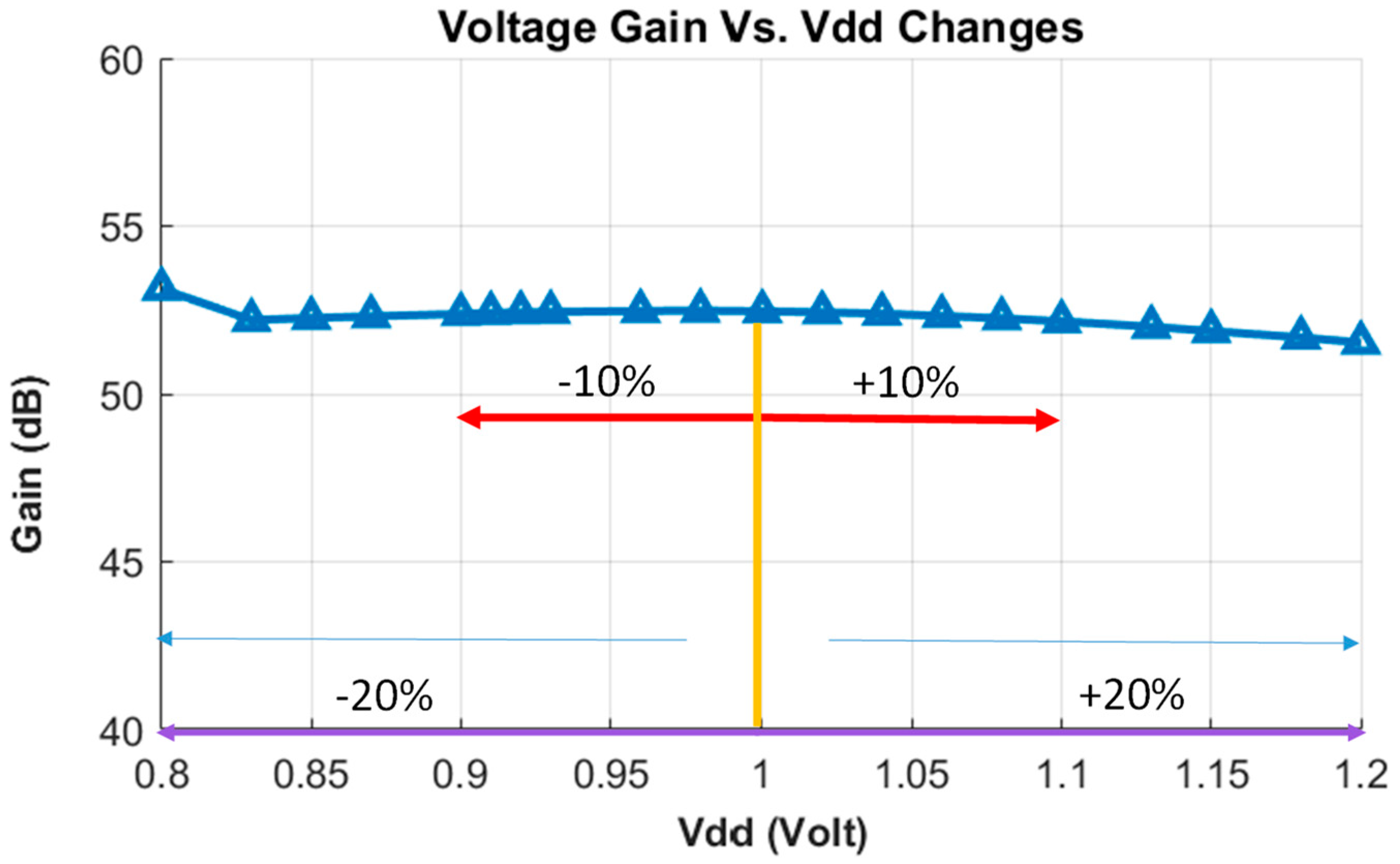
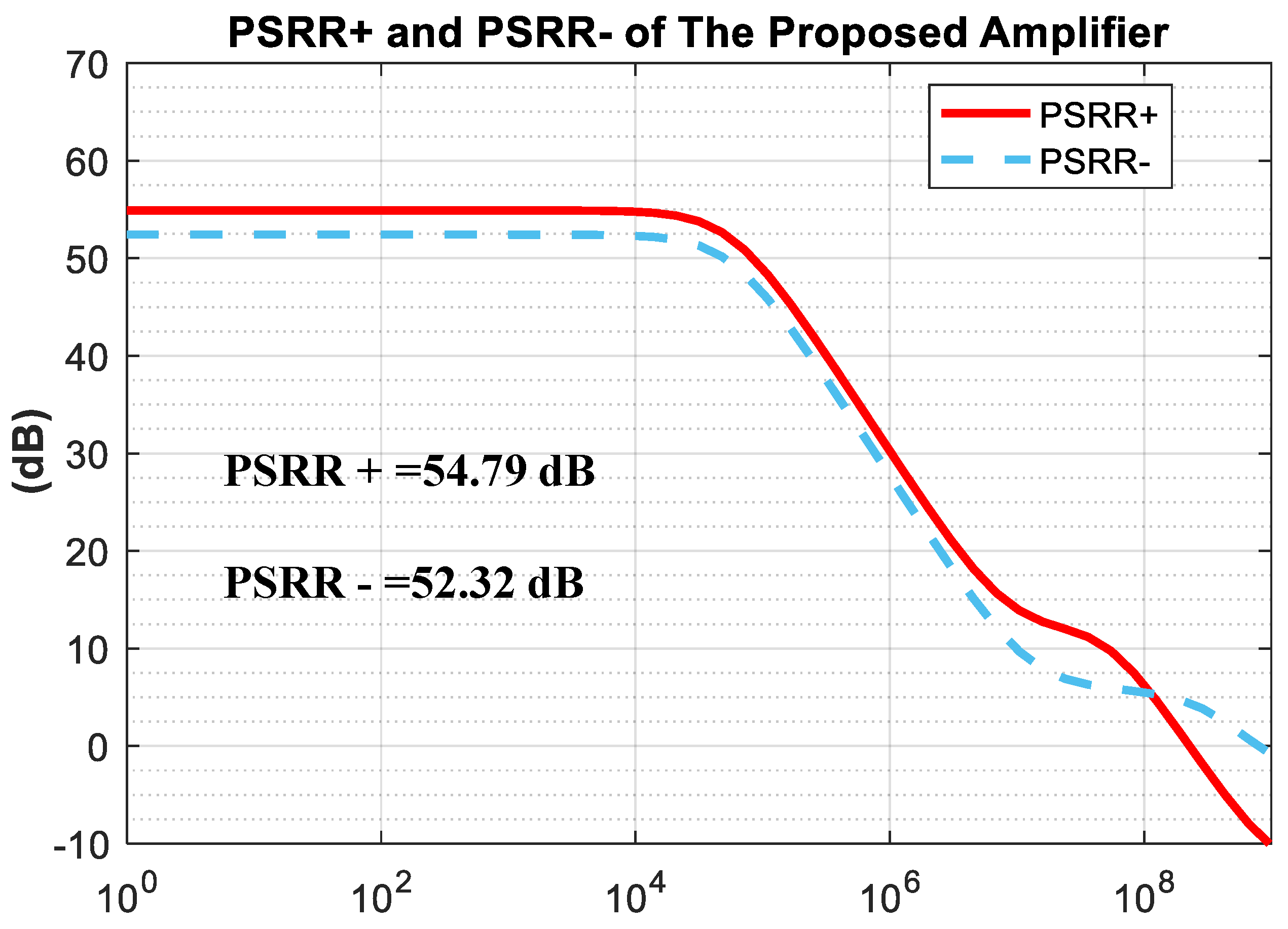
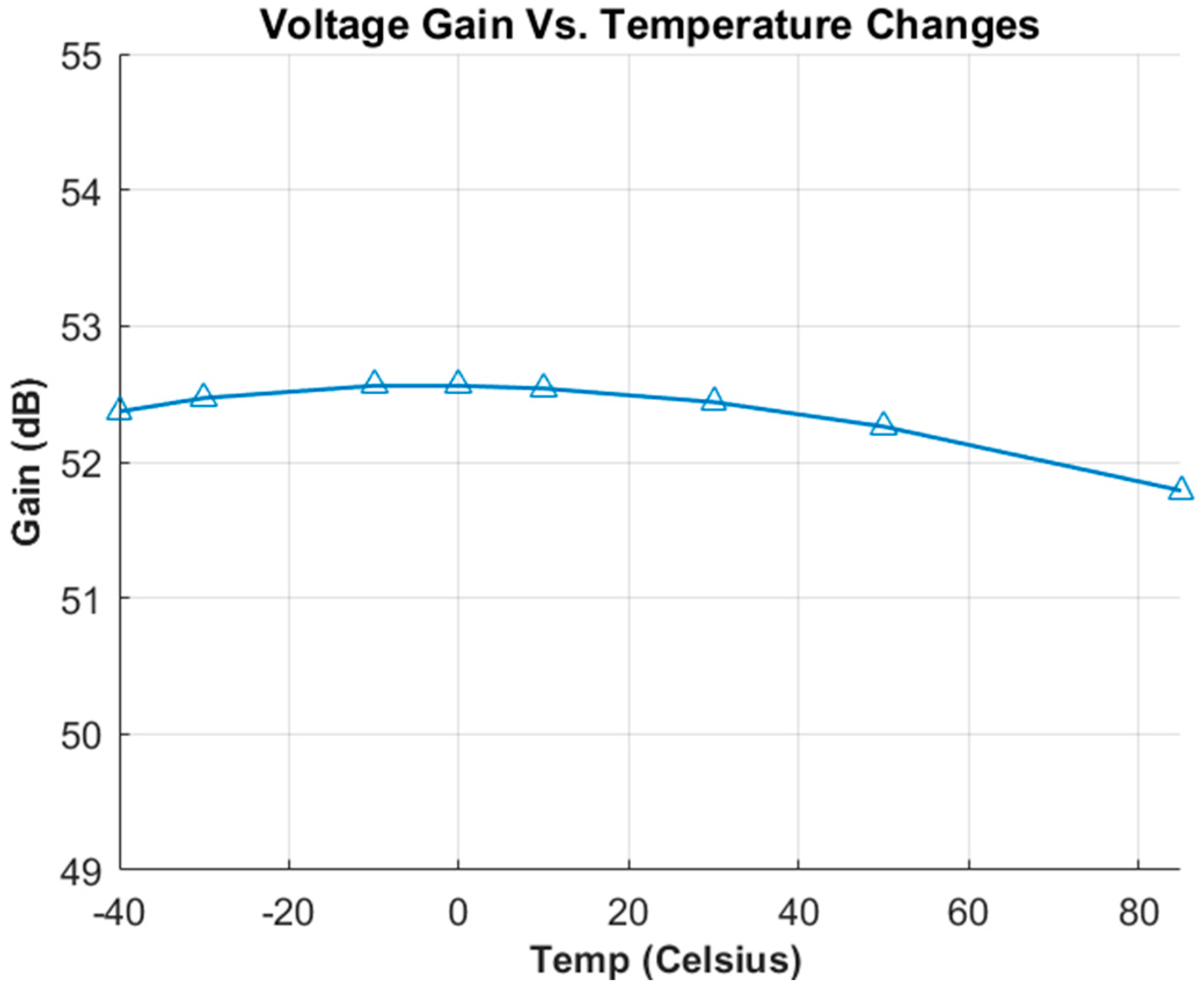
3.1.1. Analysis of the Proposed Amplifier
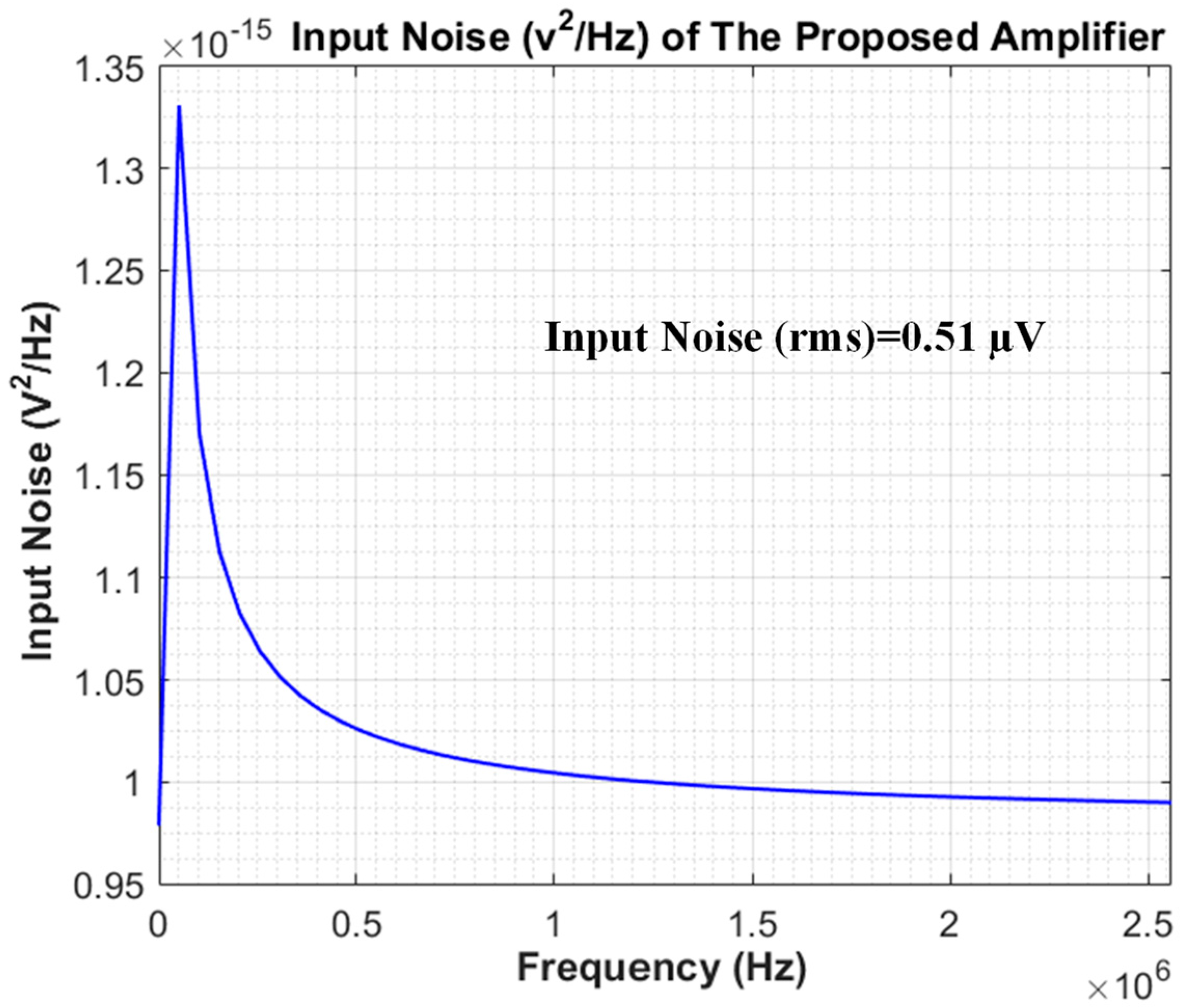
3.1.2. The Proposed Amplifier’s Noise Analysis
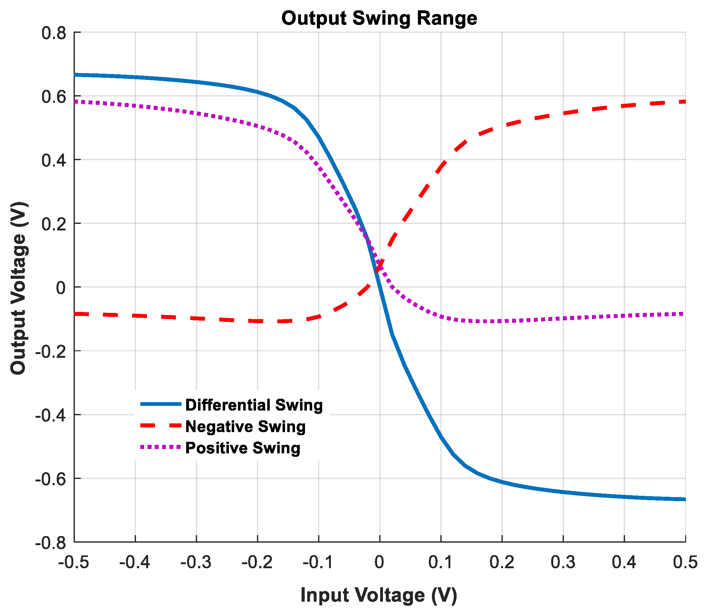
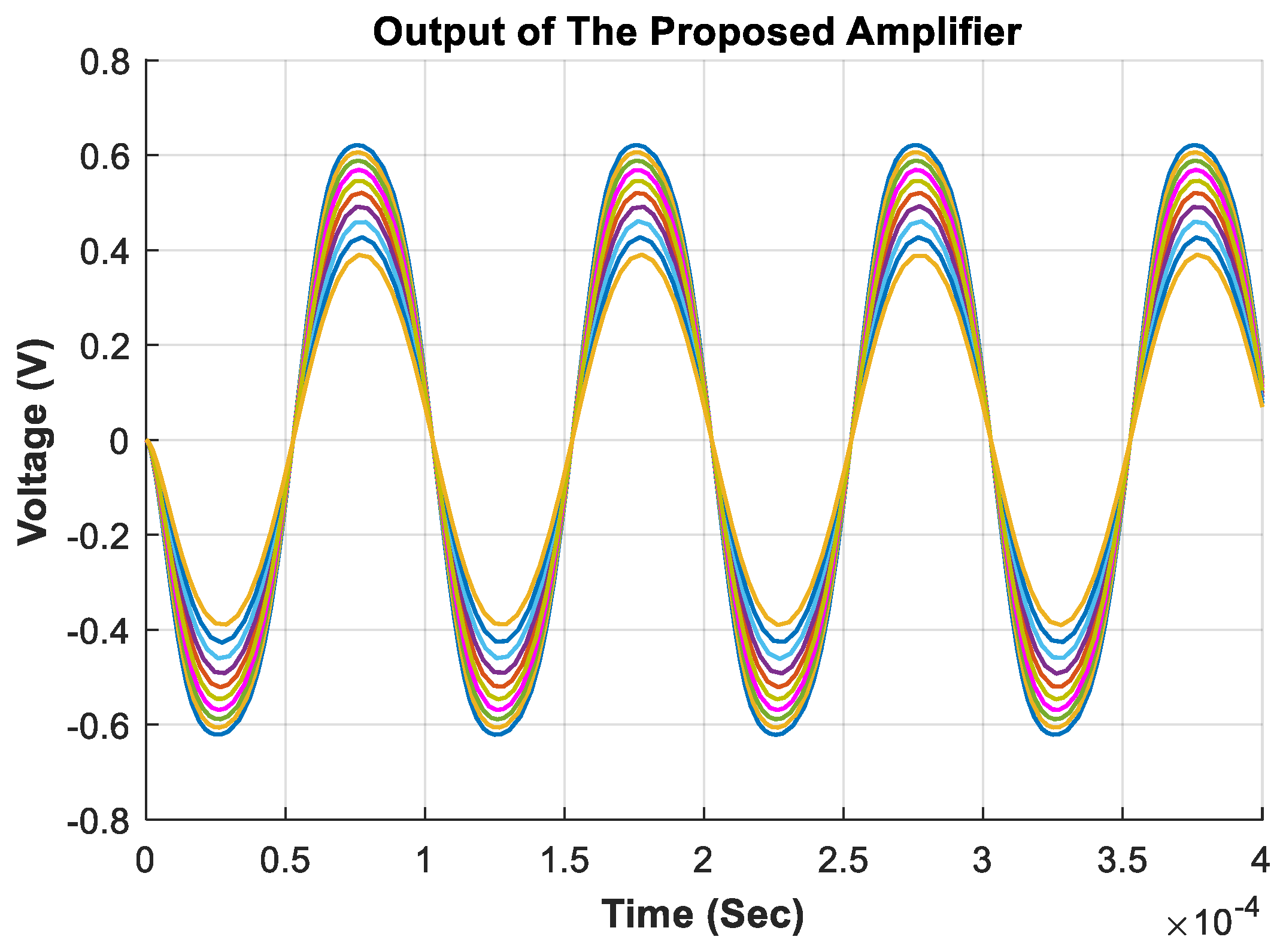
3.1.3. Output Swing Voltage of the Proposed Amplifier
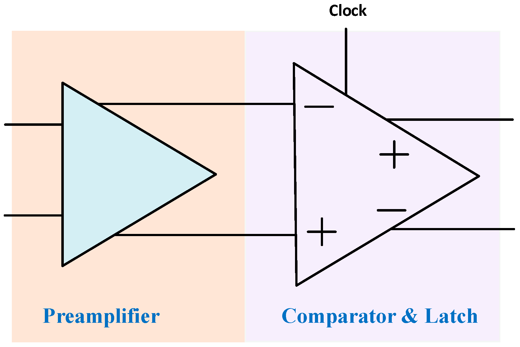
3.2. Quantizer
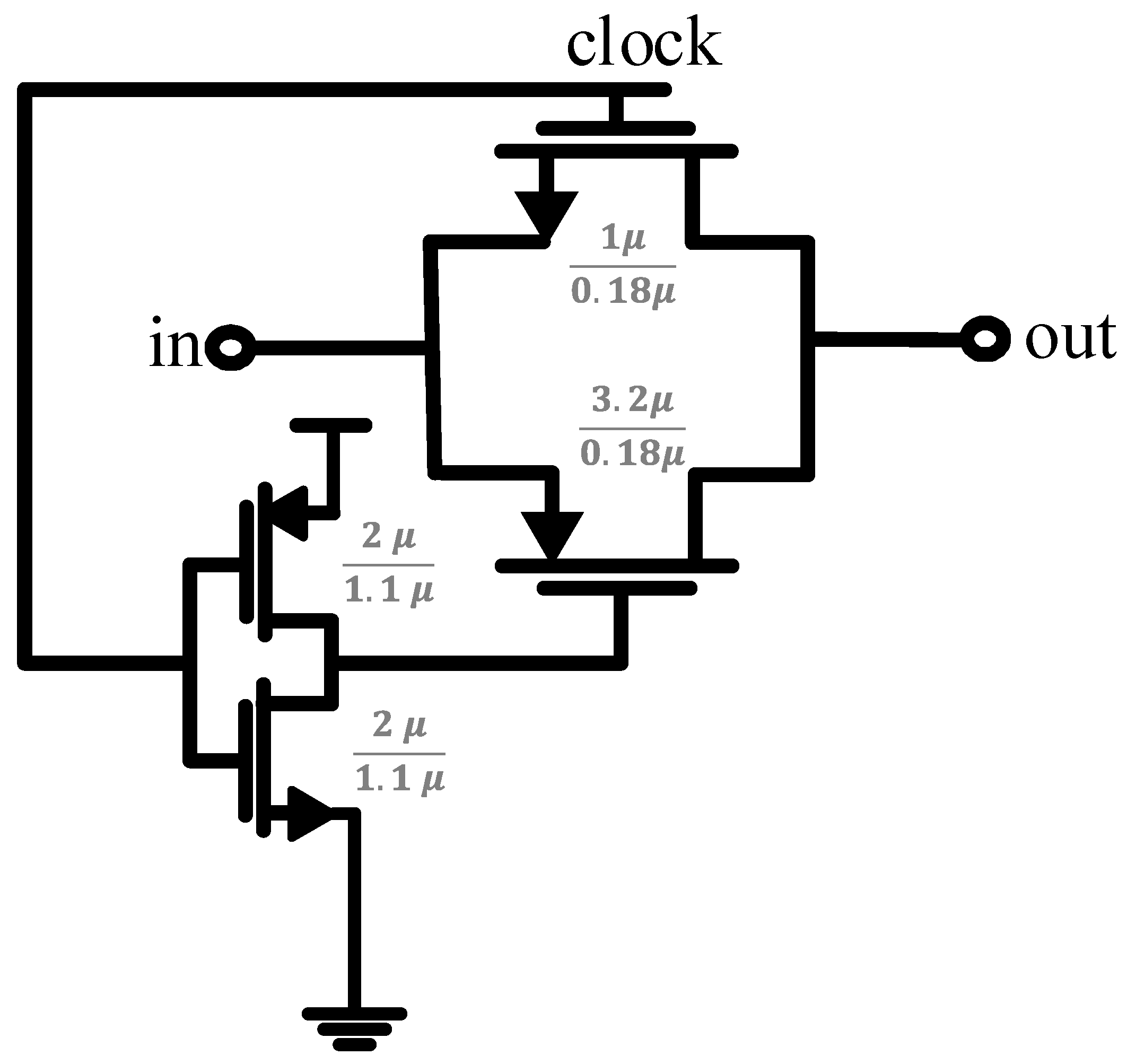
3.3. Switches
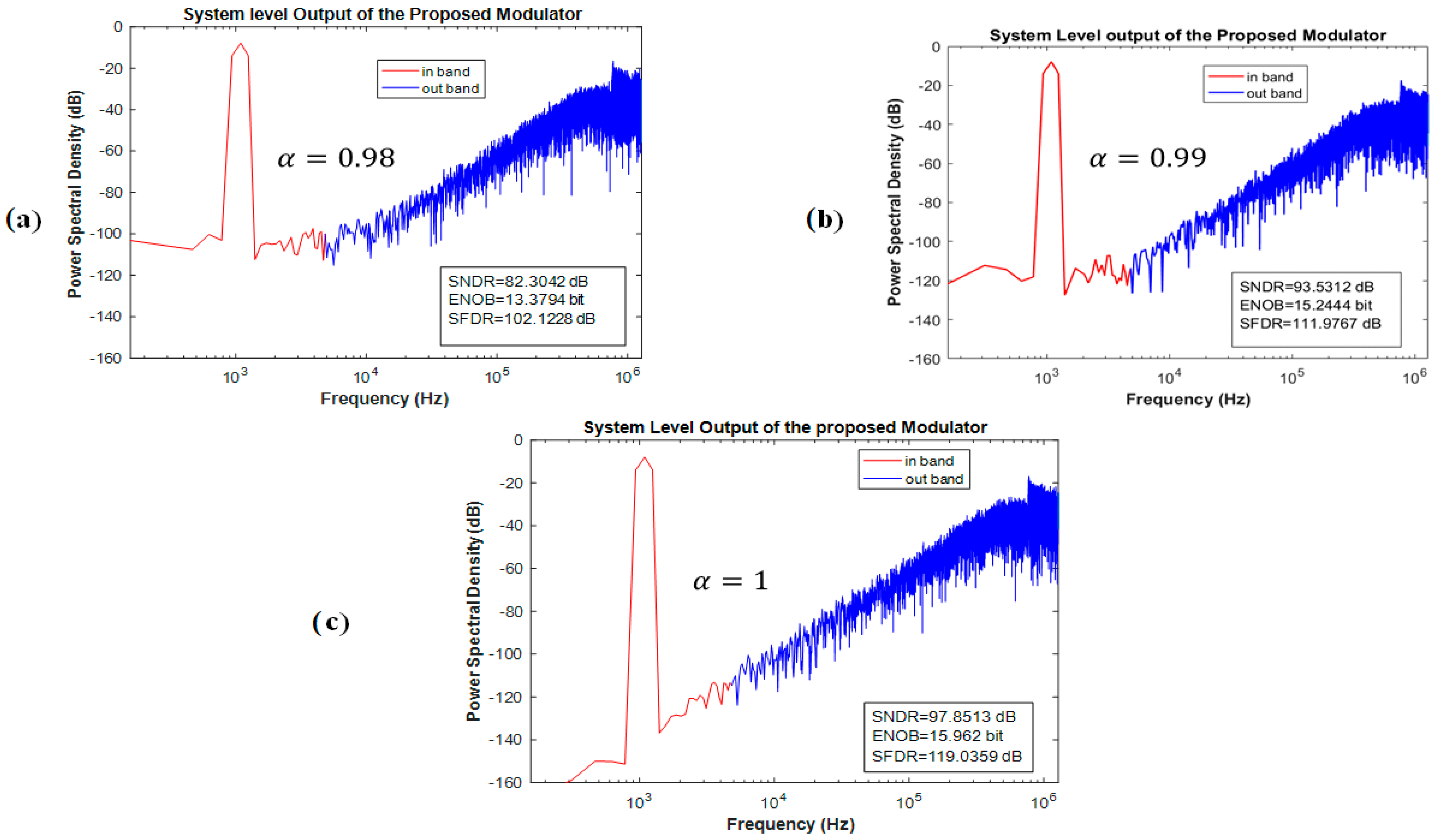
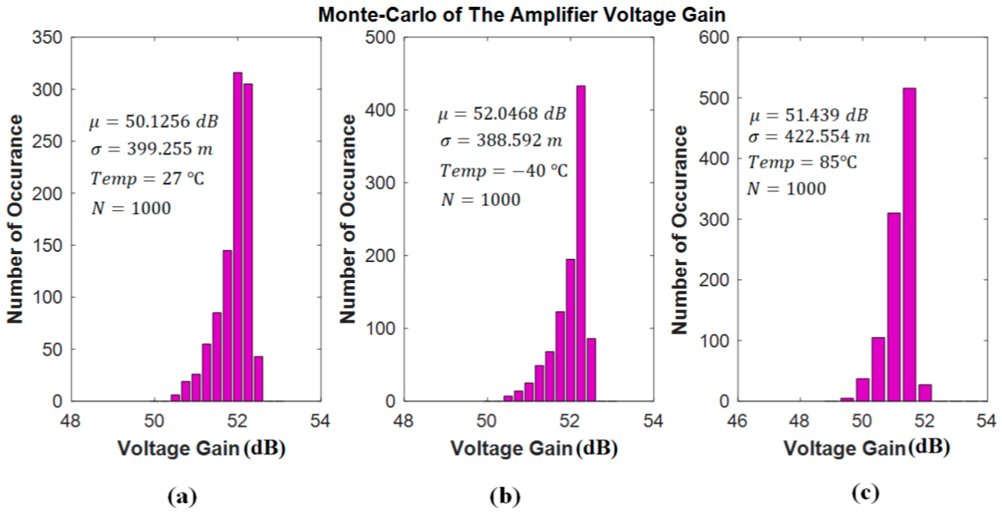
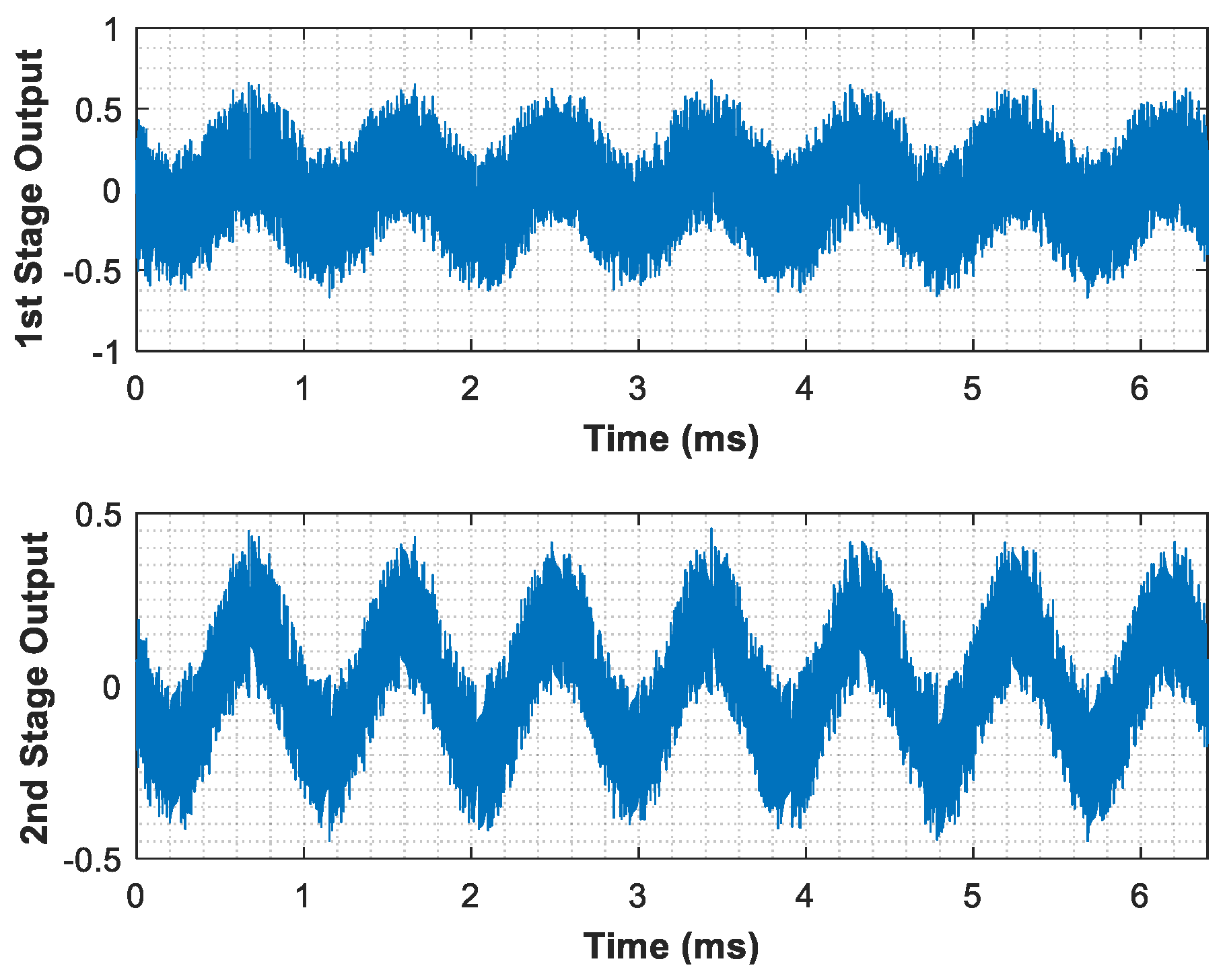
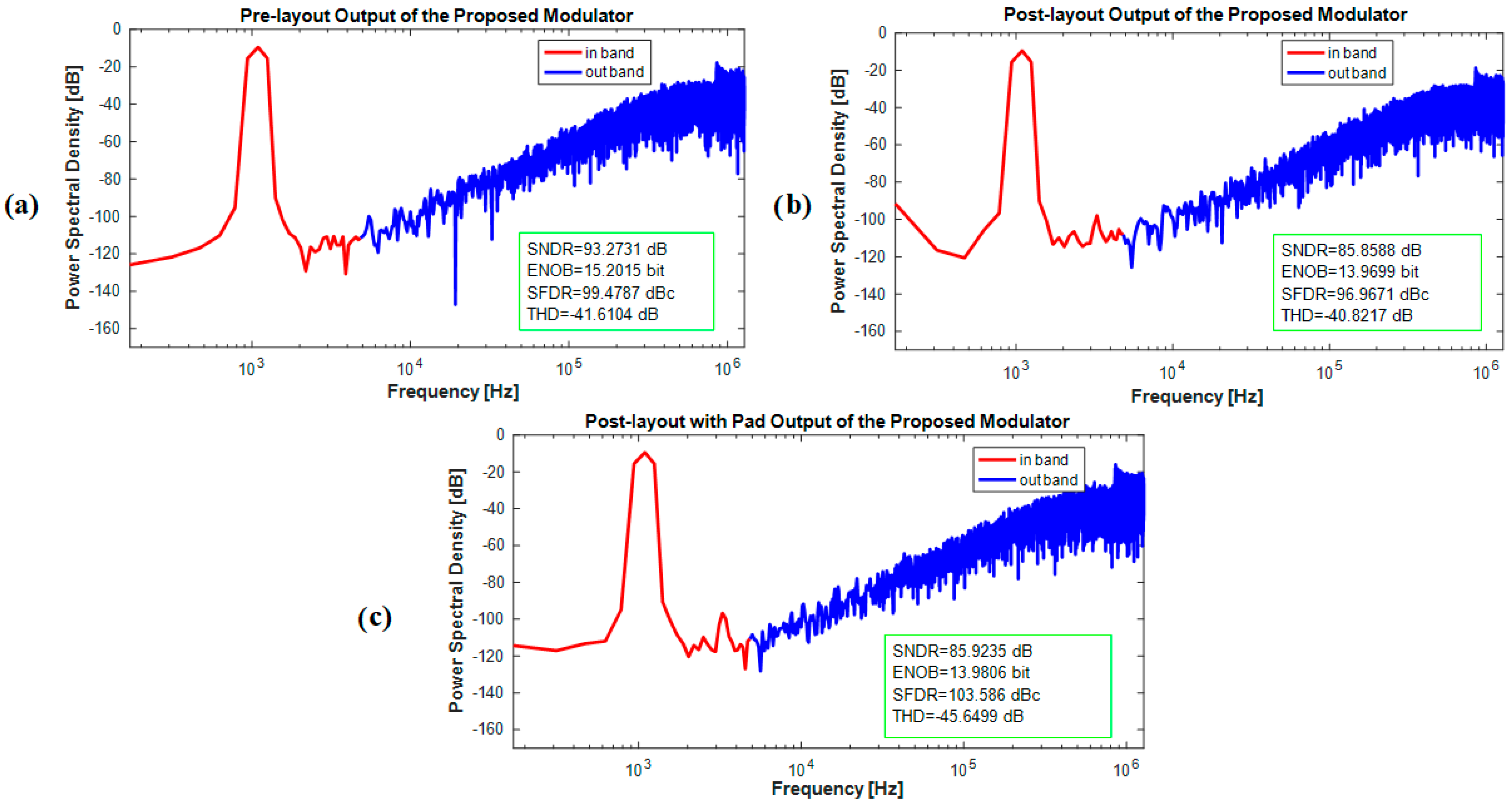
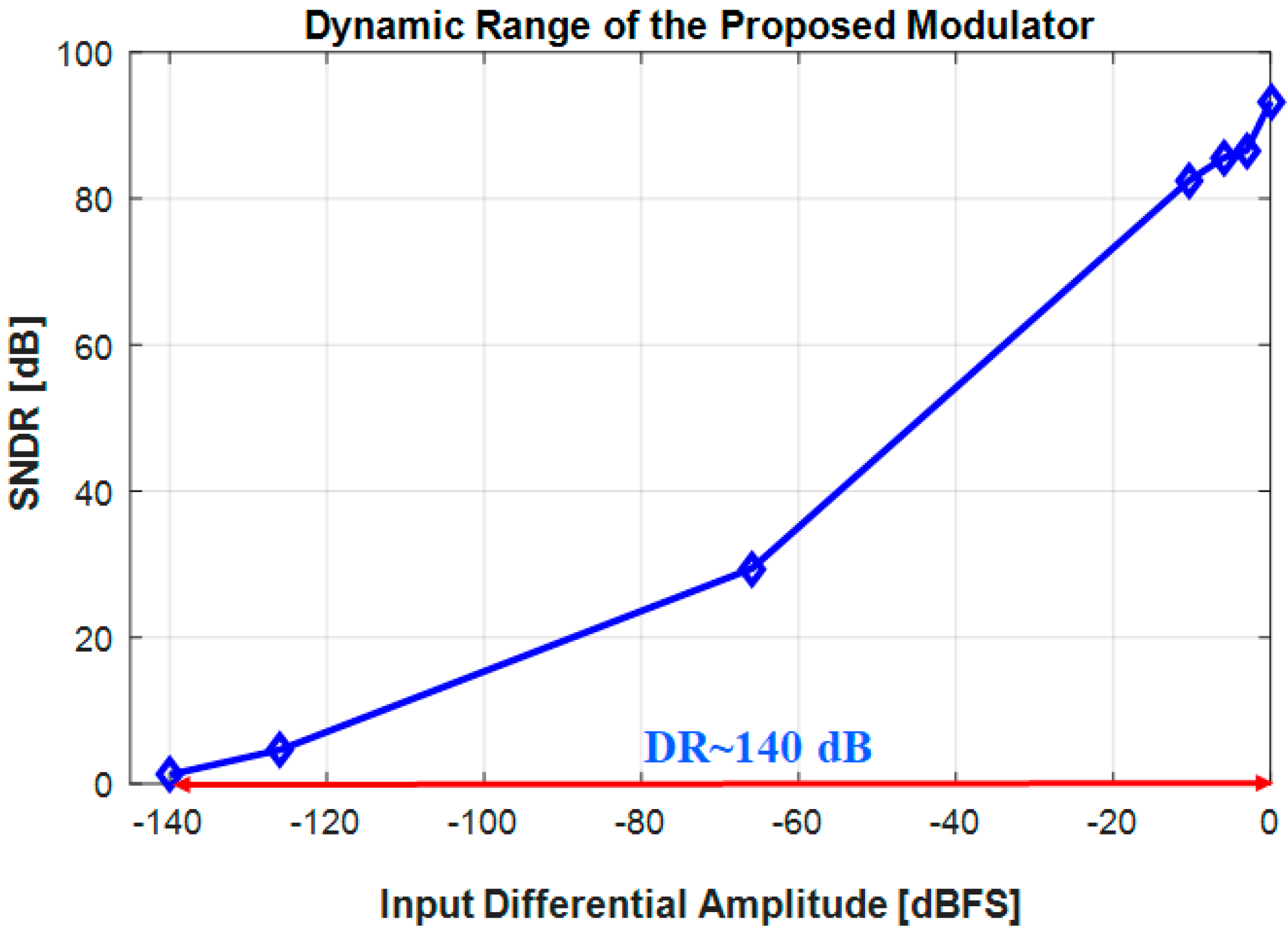
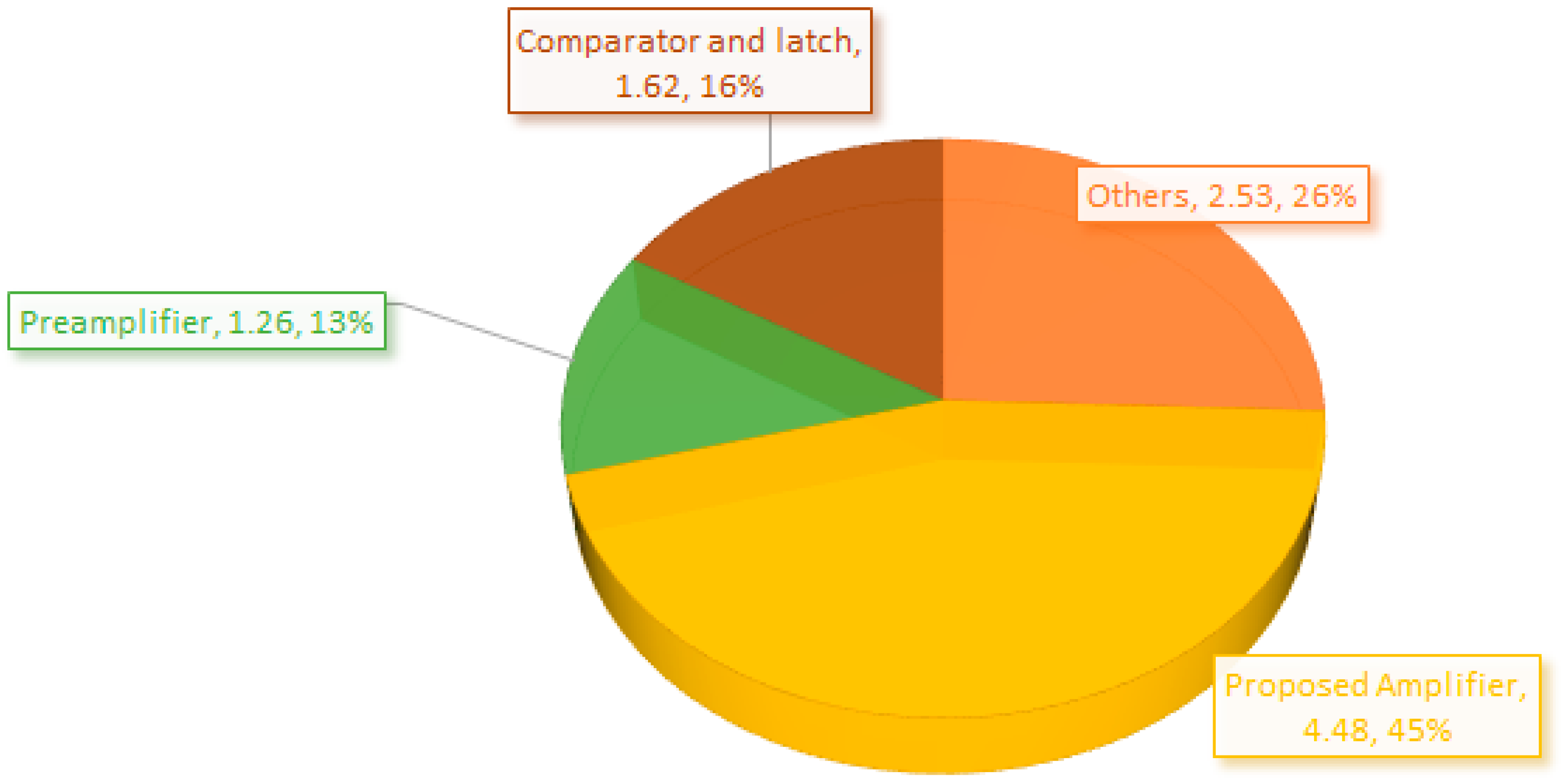
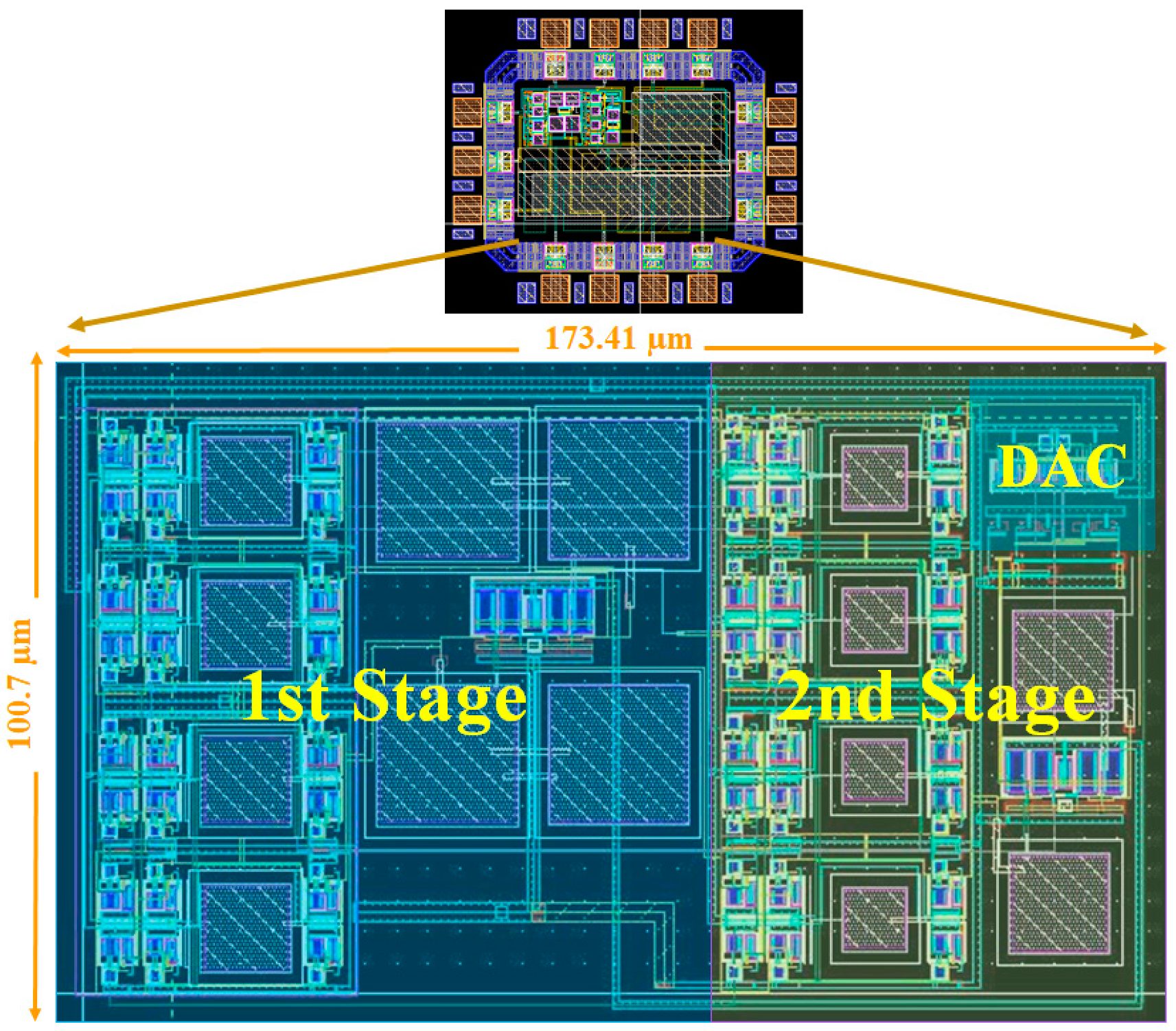
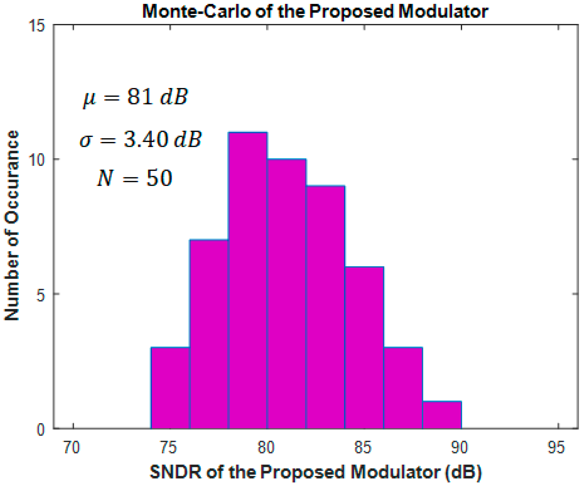
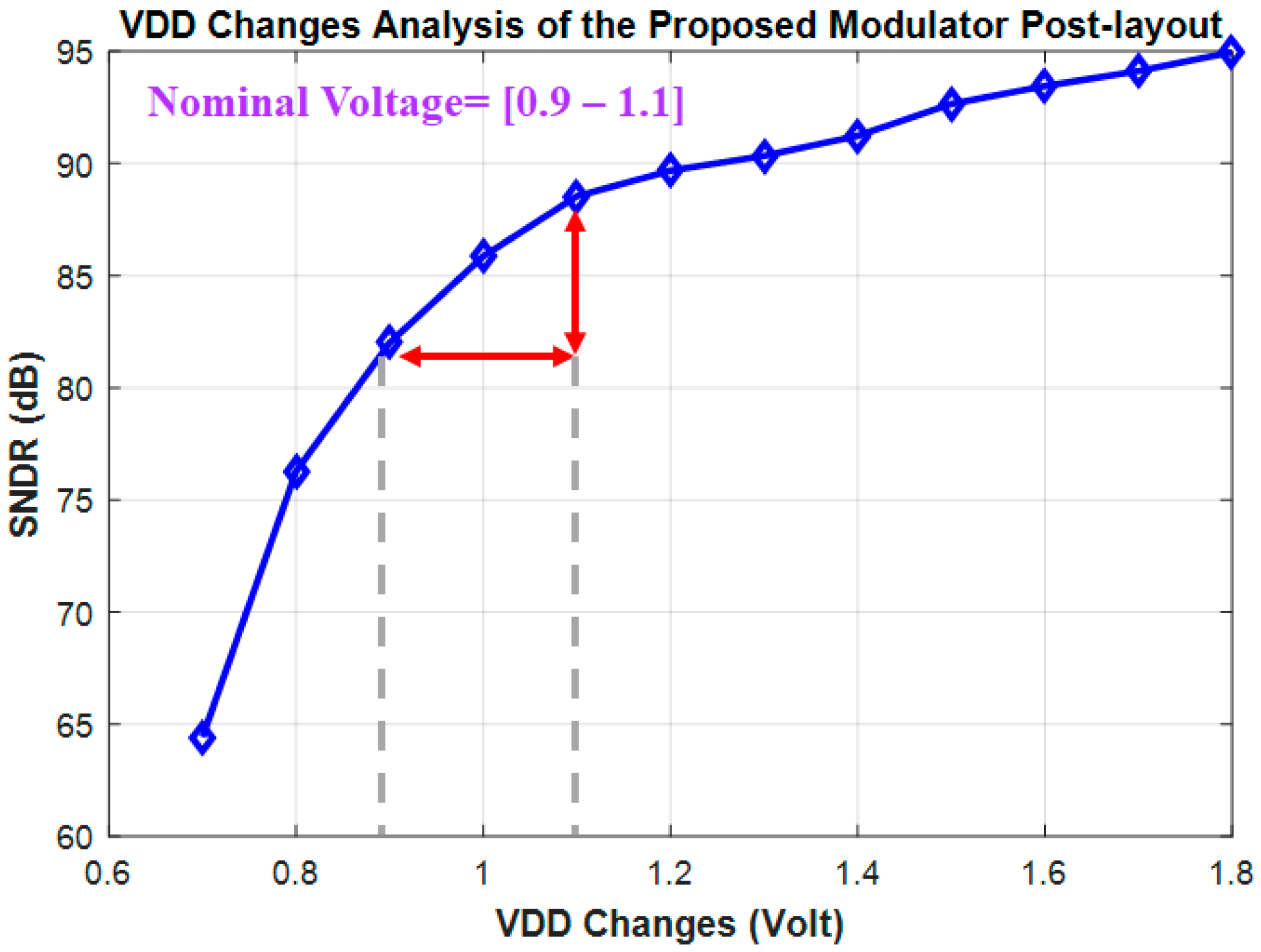
4. Simulation Results
5. Discussion
6. Conclusions
Author Contributions
Funding
Institutional Review Board Statement
Informed Consent Statement
Data Availability Statement
Conflicts of Interest
References
- Helgi, H. A 0.9-V 37-uW 98-dB DR Inverter-Based ΔΣ Modulator for Hearing Aids. Master’s Thesis, Department of Electrical and Information Technology, Faculty of Engineering, LTH, Lund University, Lund, Sweden, 2014. [Google Scholar]
- Pisha, L.; Warchall, J.; Zubatiy, T.; Hamilton, S.; Lee, C.-H.; Chockalingam, G.; Mercier, P.P.; Gupta, R.; Rao, B.D.; Garudadri, H. A Wearable, Extensible, Open-Source Platform for Hearing Healthcare Research. IEEE Access 2019, 7, 162083–162101. [Google Scholar] [CrossRef] [PubMed]
- Kanemoto, D.; Ido, T.; Taniguchi, K. A 7.5mW 101dB SNR low-power high-performance audio delta-sigma modulator utilizing opamp sharing technique. In Proceedings of the 2011 International SoC Design Conference, Jeju, Republic of Korea, 17–18 November 2011; pp. 66–69. [Google Scholar] [CrossRef]
- Kim, M.G.; Ahn, G.-C.; Hanumolu, P.K.; Lee, S.-H.; Kim, S.-H.; You, S.-B.; Kim, J.-W.; Temes, G.C.; Moon, U.-K. A 0.9 V 92 dB Double-Sampled Switched-RC Delta-Sigma Audio ADC. IEEE J. Solid-State Circuits 2008, 43, 1195–1206. [Google Scholar] [CrossRef]
- Sauerbrey, J.; Tille, T.; Schmitt-Landsiedel, D.; Thewes, R. A 0.7-V MOSFET-only switched-opamp ΣΔ modulator in standard digital CMOS technology. IEEE J. Solid-State Circuits 2002, 37, 1662–1669. [Google Scholar] [CrossRef]
- Chen, F.; Leung, B. A 0.25-mW low-pass passive sigma-delta modulator with built-in mixer for a 10-MHz IF input. IEEE J. Solid-state Circuits 1997, 32, 774–782. [Google Scholar] [CrossRef]
- Luo, H.; Han, Y.; Cheung, R.C.; Liu, X.; Cao, T. A 0.8-V 230-μW 98-dB DR Inverter-Based ΔΣ Modulator for Audio Applications. IEEE J. Solid-State Circuits 2013, 48, 2430–2441. [Google Scholar] [CrossRef]
- Lin, Y.; Ismail, M. Time-based all-digital sigma–delta modulators for nanometer low voltage CMOS data converters. Analog. Integr. Circuits Signal Process. 2012, 73, 801–808. [Google Scholar] [CrossRef]
- Sepke, T.; Fiorenza, J.; Sodini, C.; Holloway, P.; Lee, H.-S. Comparator-based switched-capacitor circuits for scaled CMOS technologies. IEEE J. Solid-State Circuits 2006, 41, 812–821. [Google Scholar] [CrossRef]
- Dhole, A.E.; Yarasu, R.B.; Lata, D.B.; Baraskar, S.S.; Shaw, D. Mathematical modeling for the performance and emission parameters of dual-fuel diesel engine using producer gas as secondary fuel. Biomass Convers. Biorefinery 2015, 5, 257–270. [Google Scholar] [CrossRef]
- Ma, S.; Liu, L.; Fang, T.; Liu, J.; Wu, N. A Discrete-Time Audio ΔΣ Modulator Using Dynamic Amplifier with Speed Enhancement and Flicker Noise Reduction Techniques. IEEE J. Solid-State Circuits 2019, 55, 333–343. [Google Scholar] [CrossRef]
- Schreier, R.; Gabor, C.T. Understanding Delta-Sigma Data Converters; IEEE: Piscataway, NJ, USA, 2005; Volume 74. [Google Scholar]
- Custódio, J.R.; Figueiredo, M.; Santin, E.; Goes, J. A CMOS Inverter-Based Self-biased Fully Differential Amplifier. IFIP Adv. Inf. Commun. Technol. 2010, 314, 541–548. [Google Scholar] [CrossRef] [Green Version]
- Chae, Y.; Han, G. Low Voltage, Low Power, Inverter-Based Switched-Capacitor Delta-Sigma Modulator. IEEE J. Solid-State Circuits 2009, 44, 458–472. [Google Scholar] [CrossRef]
- Milovanovic, V.; Zimmermann, H. On fully differential and complementary single-stage self-biased CMOS differential amplifiers. In Eurocon 2013; IEEE: Piscataway, NJ, USA, 2013; pp. 1955–1963. [Google Scholar] [CrossRef]
- Milovanović, V.; Zimmermann, H. Analyses of single-stage complementary self-biased CMOS differential amplifiers. In NORCHIP 2012; IEEE: Piscataway, NJ, USA, 2012; pp. 1–4. [Google Scholar] [CrossRef]
- Dokic, B.; Pajkanovic, A. Subthreshold operated CMOS analytic model. Parameters 2012, 2, 3. [Google Scholar]
- Bano, S.; Narejo, G.B.; Shah, S.M.U.A. Power Efficient Fully Differential Bulk Driven OTA for Portable Biomedical Application. Electronics 2018, 7, 41. [Google Scholar] [CrossRef] [Green Version]
- Yeknami, A.F.; Systemteknik, E.K.I.F. Low-Power Delta-Sigma Modulators for Medical Applications; Linkoping University: Linkoping, Sweden, 2014. [Google Scholar] [CrossRef] [Green Version]
- Custodio, J.R.; Goes, J.; Paulino, N.; Oliveira, J.P.; Bruun, E. A 1.2-V 165-/spl mu/W 0.29-mm2 Multibit Sigma-Delta ADC for Hearing Aids Using Nonlinear DACs and with Over 91 dB Dynamic-Range. IEEE Trans. Biomed. Circuits Syst. 2012, 7, 376–385. [Google Scholar] [CrossRef] [PubMed] [Green Version]
- Nilchi, A.; Johns, D.A. A Low-Power Delta-Sigma Modulator Using a Charge-Pump Integrator. IEEE Trans. Circuits Syst. I: Regul. Pap. 2013, 60, 1310–1321. [Google Scholar] [CrossRef] [Green Version]
- Porrazzo, S.S.; Morgado, A.; Bello, D.S.S.; Cannillo, F.; Van Hoof, C.; Yazicioglu, R.F.; Van Roermund, A.H.M.; Cantatore, E.E. A 155 /spl mu/W 88-dB DR Discrete-Time /spl Delta/ /spl Sigma/ Modulator for Digital Hearing Aids Exploiting a Summing SAR ADC Quantizer. IEEE Trans. Biomed. Circuits Syst. 2013, 7, 573–582. [Google Scholar] [CrossRef]
- Park, J.-E.; Hwang, Y.-H.; Jeong, D.-K. A 0.4-to-1 V Voltage Scalable ΔΣ ADC With Two-Step Hybrid Integrator for IoT Sensor Applications in 65-nm LP CMOS. IEEE Trans. Circuits Syst. II Express Briefs 2017, 64, 1417–1421. [Google Scholar] [CrossRef]
- Cho, J.S.; Rhee, J.; Kim, S.; Yang, Y.T.; Jun, J.; Kim, S.; Lee, H. A 1.2-V 108.9-dB A-Weighted DR 101.4-dB SNDR Audio ΔΣ ADC Using a Multi-Rate Noise-Shaping Quantizer. IEEE Trans. Circuits Syst. II Express Briefs 2018, 65, 1315–1319. [Google Scholar] [CrossRef]
- Liao, S.-H.; Wu, J.-T. A 1-V 175-μ W 94.6-dB SNDR 25-kHz Bandwidth Delta-Sigma Modulator Using Segmented Integration Techniques. IEEE J. Solid-State Circuits 2019, 54, 2523–2531. [Google Scholar] [CrossRef]
- Honarparvar, M.; de la Rosa, J.M.; Sawan, M. A 0.9-V 100-μW Feedforward Adder-Less Inverter-Based MASH ΔΣ Modulator With 91-dB Dynamic Range and 20-kHz Bandwidth. IEEE Trans. Circuits Syst. I Regul. Pap. 2018, 65, 3675–3687. [Google Scholar] [CrossRef]
- An, S.; Xia, S.; Ma, Y.; Ghani, A.; See, C.H.; Abd-Alhameed, R.A.; Niu, C.; Yang, R. A Low Power Sigma-Delta Modulator with Hybrid Architecture. Sensors 2020, 20, 5309. [Google Scholar] [CrossRef] [PubMed]
- Song, S.; Kim, J.; Roh, J. 100.5 dB SNDR Analog Front-End with a Resistor-Based Discrete-Time Delta-Sigma Modulator for Eliminating Switching Noise and Harmonics. IEEE Access 2021, 9, 39852–39863. [Google Scholar] [CrossRef]
- Sharma, V.; Nithin Kumar, Y.B.; Vasantha, M.H. 36 μW fourth order sigma-delta modulator using single operational amplifier. Int. J. Electron. Lett. 2021, 9, 171–186. [Google Scholar] [CrossRef]
- Fakhraie, H.; Moosazadeh, T.; Sabbaghi-Nadooshan, R.; Hassanzadeh, A. A multi-stage sigma-delta modulator based on noise-coupling and digital feed-forward techniques. Analog. Integr. Circuits Signal Process. 2021, 108, 253–266. [Google Scholar] [CrossRef]
- Matsuoka, A.; Nezuka, T.; Iizuka, T. Fully Dynamic Discrete-Time ΔΣ ADC Using Closed-Loop Two-Stage Cascoded Floating Inverter Amplifiers. IEEE Trans. Circuits Syst. II Express Briefs 2021, 69, 944–948. [Google Scholar] [CrossRef]
- Kumar, R.S.A.; Krishnapura, N.; Banerjee, P. Analysis and Design of a Discrete-Time Delta-Sigma Modulator Using a Cascoded Floating-Inverter-Based Dynamic Amplifier. IEEE J. Solid-State Circuits 2022, 57, 3384–3395. [Google Scholar] [CrossRef]
- Han, Y.; Liu, W.; Zhang, X.; Wang, X.; Liu, X.; Liu, Y. A Wide Dynamic Range Sigma-Delta Modulator for EEG Acquisition Using Randomized DWA and Dynamic-Modulated Scaling-Down Techniques. Sensors 2022, 23, 201. [Google Scholar] [CrossRef]
- Yousefirad, M.; Yavari, M. A fully dynamic third-order EF-CIFF noise-shaping SAR ADC with NTF zeros optimization and passive integration. AEU Int. J. Electron. Commun. 2022, 157, 154422. [Google Scholar] [CrossRef]


| Coefficient | Value |
|---|---|
| a1,2 | 1 |
| C1 | 0.4 |
| C2 | 0.8 |
| Capacitor | Value |
|---|---|
| Cs1A,1B | 0.2 pF |
| Cs2A,2B | 0.1 pF |
| CI1 | 1 pF |
| CI2 | 0.25 pF |
| Transistor | M1,3 | M2,4 | M5 | M6 |
|---|---|---|---|---|
| Transistor | M1,3 (pMOS) | M2,4 (nMOS) | M5 (pMOS) | M6 (nMOS) | |
|---|---|---|---|---|---|
| Parameter | |||||
| ID | 482.79 nA | 482.79 nA | 1.93 µA | 1.93 µA | |
| Vgs | −480.57 mV | 489.25 mV | −494.42 mV | 505.58 mV | |
| Vth | −452.54 mV | 461.88 mV | −509.88 mV | 525.29 mV | |
| Vds | −474.99 mV | 494.83 mV | −19.43 mV | 10.75 mV | |
| Region | Saturation | Saturation | Subthreshold | Subthreshold | |
| Temp (°C) | −40 | 27 | 85 | |
|---|---|---|---|---|
| Corner | ||||
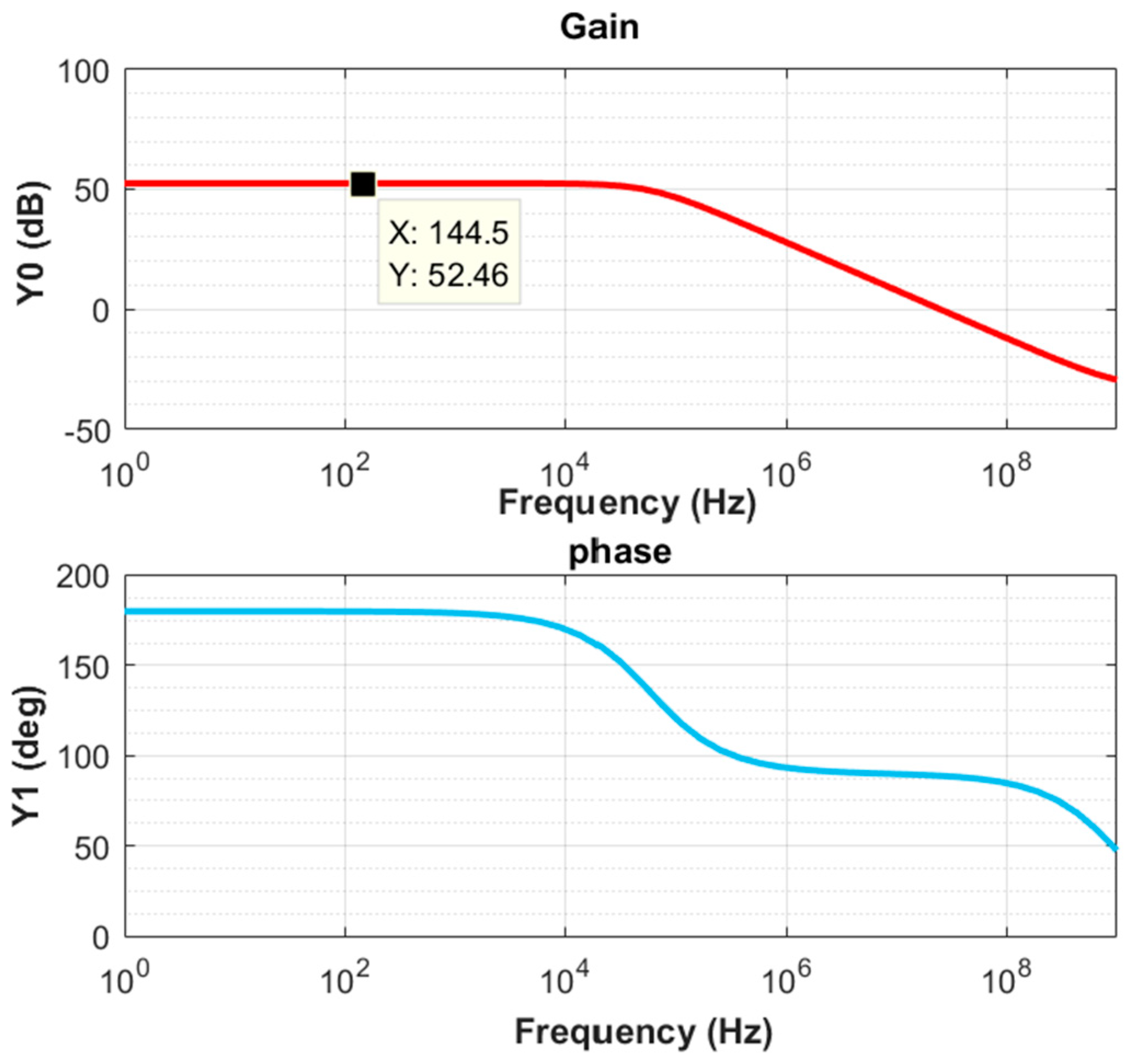
| TT | 52.37 | 52.46 | 51.79 | |
| FF | 50.4 | 49.9 | 48.97 | |
| SS | 52.04 | 52.69 | 52.46 | |
| FS | 50.82 | 50.72 | 49.72 | |
| SF | 50.96 | 50.91 | 49.56 | |
| Parameters | Value |
|---|---|
| Power Supply (V) | 1 |
| Power Consumption (µV) | 1.93 |
| Tech (nm) | 180 |
| Gain (dB) | 52.46 |
| Peak-to-peak Swing Voltage (V) | 1.01 |
| Phase Margin (degree) | 88.86 |
| Slew Rate + (V/µSec) | 104.68 |
| Slew Rate − (V/µSec) | −119.78 |
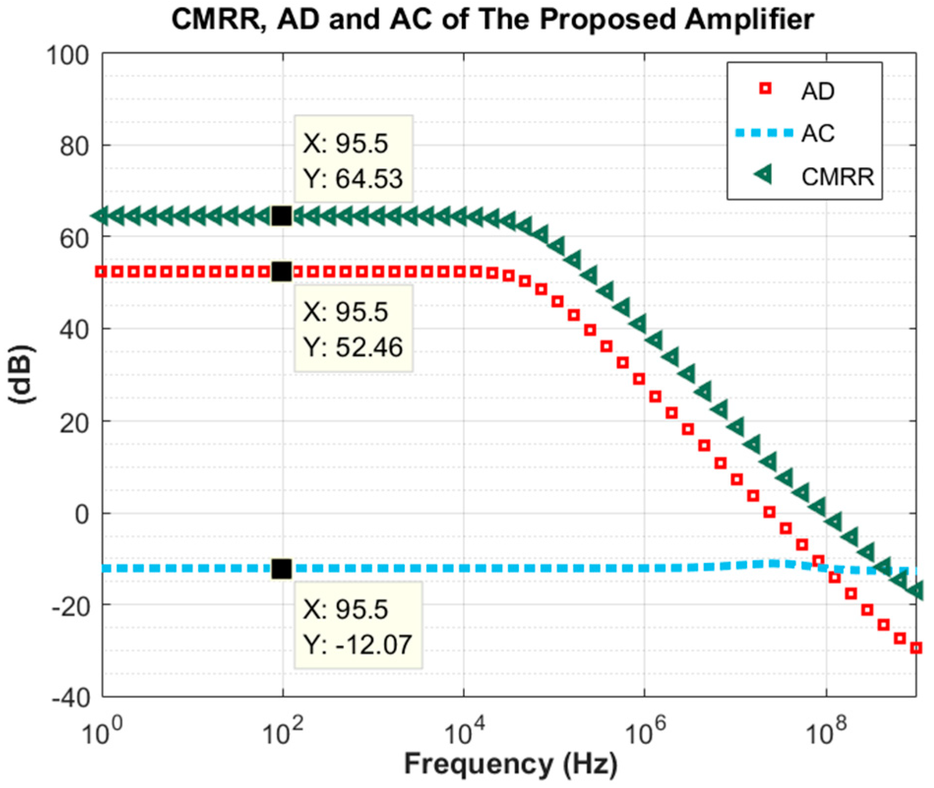
| PSRR + (dB) | 54.79 |
| PSRR − (dB) | 52.32 |
| CMRR | 64.53 |
| RMS Input Noise (µV) | 0.51 |
| SNDR (dB) | 77.25 |
| SFDR (dB) | 73.35 |
| THD (dB) | −77.25 |
| SNDR (dB) | SNR (dB) | THD (dB) |
|---|---|---|
| 71.5 | 89.5 | −42.23 |
| Modulator Parameters | Value |
|---|---|
| Power Supply (V) | 1 |
| Power Consumption (µV) | 9.9 |
| Tech (nm) | 180 |
| Peak SNDR (dB) | 93.27 |
| DR (dB) | 140 |
| Order | 2nd order |
| Structure | Double Sampling CIFB |
| FOMs | 183.31 |
| FOMw (fJ/step) | 1.31 |
| FOMDR (dB) | 230.04 |
| Area (mm2) |
| Corner | Temp (°C) | SNDR (dB) | SFDR (dB) | THD (dB) | Precision (Bits/Sample) | |
|---|---|---|---|---|---|---|
| Post-layout Corner Test | TT | 27 | 85.86 | 96.98 | −40.82 | 13.97 |
| FF | 27 | 94.75 | 102.24 | −40.88 | 15.45 | |
| SS | 27 | 69.25 | 101.68 | −39.77 | 11.21 | |
| SF | 27 | 69.39 | 84.19 | −46.19 | 11.23 | |
| FS | 27 | 83.98 | 98.32 | −45.48 | 13.66 |
| Ref. | Vdd [V] | BW [KHz] | OSR | Fs [MHz] | SNDR (dB) | DR (dB) | Pow. (μW) | FOMS (dB) | FOMDR (dB) | FOMw (fJ/step) | Tech (nm) | Result | Year |
|---|---|---|---|---|---|---|---|---|---|---|---|---|---|
| [20] | 1.2 | 20 | 32 | 1.28 | 72.5 | 91 | 165 | 155.5 | 171.84 | 92 | 130 | Measure | 2012 |
| [21] | 1.2 | 10 | 128 | 2.56 | 87.8 | 90 | 148 | 166 | 168.3 | 36 | 180 | Measure | 2012 |
| [22] | 1.8 | 10 | 64 | 1.28 | 84.4 | 88 | 570 | 156.84 | 160.44 | 210.1 | 180 | Measure | 2013 |
| [23] | 0.5 | 20 | 51.2 | 2 | 60.8 | 70.1 | 43.4 | 147.44 | 156.74 | 121 | 65 | Measure | 2017 |
| [24] | 1.2 | 20 | 76.8 | 3.07 | 101.4 | 105.7 | 3500 | 168.97 | 173.27 | 91 | 130 | Measure | 2018 |
| [25] | 1 | 25 | 100 | 5 | 94.6 | 98.5 | 175 | 176.15 | 180 | 7.97 | 65 | Measure | 2018 |
| [26] | 0.9 | 20 | 128 | 5.12 | 86.4 | 91 | 103.4 | 169.27 | 173.86 | 150 | 180 | Measure | 2018 |
| [11] | 0.8 | 24 | 64 | 3.07 | 89.6 | 91 | 49.6 | 176.6 | 178 | 50.6 | 65 | Measure | 2019 |
| [10] | 1.2 | 20 | 64 | 2.56 | 81.17 | NA | 54 | 166.86 | NA | 14.44 | 180 | Simulate | 2019 |
| [27] | 1.8 | 25 | 128 | 3.2 | 106 | NA | 3650 | 169.4 | NA | 44.75 | 180 | Measure | 2020 |
| [28] | 1.8 | 25 | 256 | 12.8 | 106.1 | 102.3 | 2200 | 171.16 | 172.86 | 50.23 | 180 | Measure | 2021 |
| [29] | 1.8 | 10 | 16 | 0.32 | 74.24 | 78 | 36 | 158.68 | 162.44 | 42.75 | 180 | Simulate | 2021 |
| [30] | 1.8 | 10,000 | 8 | 160 | 98.4 | 101 | 26,300 | 184.2 | 186.8 | 1.93 | 180 | Simulate | 2021 |
| [31] | 1 | 19.5 | 256 | 10 | 88.5 | 91.7 | 43.5 | 175 | 178.2 | 51.2 | 180 | Measure | 2021 |
| [32] | 1.8 | 24 | 64 | 3.07 | 96.2 | 98 | 340 | 174.7 | 176.49 | 13.42 | 180 | Measure | 2022 |
| [33] | 1.8 | 1.5 | 341.3 | 1.024 | 118.1 | 126 | 1600 | 177.8 | 185.72 | 81.17 | 180 | Simulate | 2022 |
| [34] | 1.1 | 156.25 | 8 | 2.5 | 83.1 | 84 | 70.3 | 176.57 | 177.47 | 1.93 | 180 | Simulate | 2022 |
| This work | 1 | 10 | 128 | 2.56 | 93.27 | 140 | 9.9 | 183.31 | 230.04 | 1.31 | 180 | Simulate | 2023 |
Disclaimer/Publisher’s Note: The statements, opinions and data contained in all publications are solely those of the individual author(s) and contributor(s) and not of MDPI and/or the editor(s). MDPI and/or the editor(s) disclaim responsibility for any injury to people or property resulting from any ideas, methods, instructions or products referred to in the content. |
© 2023 by the authors. Licensee MDPI, Basel, Switzerland. This article is an open access article distributed under the terms and conditions of the Creative Commons Attribution (CC BY) license (https://creativecommons.org/licenses/by/4.0/).
Share and Cite
Alizadeh Zanjani, S.; Jannesari, A.; Torkzadeh, P. 9.9 µW, 140 dB DR, and 93.27 dB SNDR, Double Sampling ΔΣ Modulator Using High Swing Inverter-Based Amplifier for Digital Hearing Aids. Electronics 2023, 12, 1747. https://doi.org/10.3390/electronics12071747
Alizadeh Zanjani S, Jannesari A, Torkzadeh P. 9.9 µW, 140 dB DR, and 93.27 dB SNDR, Double Sampling ΔΣ Modulator Using High Swing Inverter-Based Amplifier for Digital Hearing Aids. Electronics. 2023; 12(7):1747. https://doi.org/10.3390/electronics12071747
Chicago/Turabian StyleAlizadeh Zanjani, Shima, Abumoslem Jannesari, and Pooya Torkzadeh. 2023. "9.9 µW, 140 dB DR, and 93.27 dB SNDR, Double Sampling ΔΣ Modulator Using High Swing Inverter-Based Amplifier for Digital Hearing Aids" Electronics 12, no. 7: 1747. https://doi.org/10.3390/electronics12071747