1. Introduction
In recent years, recurrent neural nets have been widely used in tasks such as speech recognition [
1], due to their excellent performance. Long short-term memory (LSTM) is one of the most popular recurrent neural networks. A central processing unit (CPU) and graphics processing unit (GPU) are common LSTM hardware computing platforms. Due to a large number of calculations and complex data dependencies in LSTM, it is often not so efficient to calculate LSTM through CPU or GPU. When performing specific LSTM calculations, the utilization of CPU and GPU is usually relatively low. Due to the aforementioned drawbacks of CPU and GPU, some energy-efficient platforms are used as accelerators for LSTM forward inference, such as field-programmable gate arrays (FPGAs) and application-specific integrated circuits (ASICs). ASICs are highly energy efficient. For example, Google’s TPUv4i [
2] has a performance of up to 138 tera floating point operations per second (TFLOPS). However, ASICs are inflexible and expensive to manufacture. Specific ASIC chips may not keep up with the development of neural network algorithms.
FPGAs have achieved a good balance in terms of reconfigurability, flexibility, performance, and power consumption. At present, many researchers use FPGAs to accelerate LSTM [
3,
4,
5,
6,
7,
8,
9,
10,
11,
12,
13,
14,
15,
16,
17,
18,
19,
20,
21,
22,
23]. Some works reduce the storage space of LSTM by compressing and quantizing the weight of LSTM, and then storing all the weight on the chip [
9,
11]. In work [
9], the LSTM model is compressed using the block-circulant matrix technology so that the model parameters can be stored on the on-chip block random access memory (BRAM) of the FPGA. In [
11], the bank-balanced sparsity method was used to reduce the number of parameters, so that all weights were stored on-chip in the small model. Some works store weights in off-chip memory and reduce bandwidth requirements through data reuse [
16,
19]. The authors of [
19] split the weight matrix into multiple blocks, and each block could be used for a batch of input data, which increased data reuse. Addressing edge computing scenarios, the authors of [
12] focused on using embedded FPGAs to accelerate lightweight LSTM. However, most works use FPGAs to accelerate an LSTM model, which cannot effectively accelerate some multi-layer LSTM. Most of them use different computing units to calculate different matrix multiplications of an LSTM, to those used to calculate operations such as element-wise multiplication and element-wise addition in LSTM.
In this paper, we propose an instruction-driven accelerator. For large LSTM and multi-layer LSTM, LSTM can be decomposed into multiple groups of small calculations through a series of instructions. Our hardware consists of matrix multiplication units and post-processing units, that compute element-wise multiplication, element-wise addition, etc. Several optimization techniques are used to improve performance and utilize resources efficiently.
The contributions of this work are summarized as follows.
The matrix multiplication units in the accelerator are cascaded, to simultaneously compute multiple user input data. The matrix multiplication units reduce register usage through a time-staggered data readout strategy.
In the post-processing unit, only two DSPs with resource sharing are used, to complete various types of calculations such as element-wise multiplication and batch normalization, which reduces the resource usage of the post-processing unit.
A domain-specific instruction set is designed to compute complex operations in LSTM. A complex LSTM is executed by splitting it into a sequence of instructions.
For a case study, experiments have been performed on the Xilinx Alevo U50 card. The results show that our design achieves a performance of 2036 giga operations per second (GOPS) and the utilization of the hardware reaches 86.1%.
The rest of the paper is organized as follows.
Section 2 introduces the background.
Section 3 presents the hardware architecture design.
Section 4 describes the detailed instruction design.
Section 5 gives an analysis of the experimental results.
Section 6 concludes the paper.
2. Background
LSTM was first proposed in 1997 [
24], and there have been many variants of LSTM since then. Google LSTM [
25] is one variant that has been widely used. Therefore, without loss of generality, this paper uses Google LSTM as an example.
Figure 1 shows the network structure of LSTM.
Compared with the standard LSTM, Google LSTM has additional peephole connections and a projection layer. This structure has a better effect on deep networks. The input of an LSTM is a sequence
;
represents the input vector at time
t. The output of an LSTM is a sequence
;
denotes the output vector at time
t. The operation of an LSTM can be expressed as:
where
,
,
,
,
represent input gate, forget gate, output gate, cell state, and cell output, respectively. ⊙ represents element-wise multiplication. + denotes element-wise addition.
denotes represents the weight matrix.
denotes the bias used in the matrix multiplication operation.
denotes the sigmoid activation function.
represents the tanh activation function.
The input gate controls the proportion of input information transmitted to the cell state at the current time step. The output gate controls the proportion of the cell state transmitted to the output. The forget gate controls the proportion of information forgotten and retained by the cell state. Cell state saves previous information. Because the number of units in the projection layer is less than that of the hidden units, the projection layer can control the total number of parameters, while allowing the number of hidden units to be increased. The output layer calculates the final output.
LSTM will save previous information and be able to learn the relationship between data at different times, so that LSTM can process sequential data such as voice data. Therefore, LSTM is widely used in tasks such as speech recognition, machine translation, etc.
Next, we will introduce some principles of hardware acceleration for computing. Common methods of hardware acceleration include pipelining, loop unrolling, loop tiling, and loop interchange, among others. Pipelining can increase the operating frequency of the system. Loop unrolling can improve parallelism during acceleration. In the case of insufficient on-chip storage resources, loop tiling can process part of the data at a time. Reasonable loop interchange can improve data reuse and optimize data movements and memory access. In computing tasks, multiple computing units of FPGA can be used for parallel processing. In the calculation process, improving the effective utilization of computing resources is helpful to the final performance.
3. Hardware Architecture
Our complete design consists of a hardware accelerator and corresponding instruction set design.
Section 3 introduces the design of each module in the hardware part.
3.1. Overall Architecture
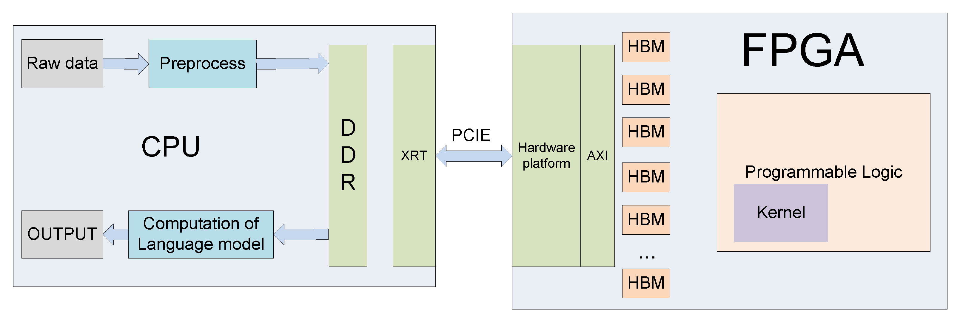
Our design consists of a host and a kernel. The host program is written in C++ and runs on the CPU, and the kernel program is written in Verilog and runs on the FPGA. As shown in
Figure 2, data pre-processing, including feature extraction, and post-processing, including language models, are all calculated in the host, while LSTM computing is in the kernel. When the system starts to work, the host pre-processes the data first and then sends instructions, weights, parameters, the activation function table, and the pre-processed input data to high bandwidth memory (HBM). Then, the kernel starts executing the instructions. When the kernel finishes computing, the kernel notifies the host and puts the result on the HBM. Then, the host will perform the remaining calculations, such as the calculation of the language model, and notify the kernel to proceed with the next operation.
3.2. Kernel Architecture
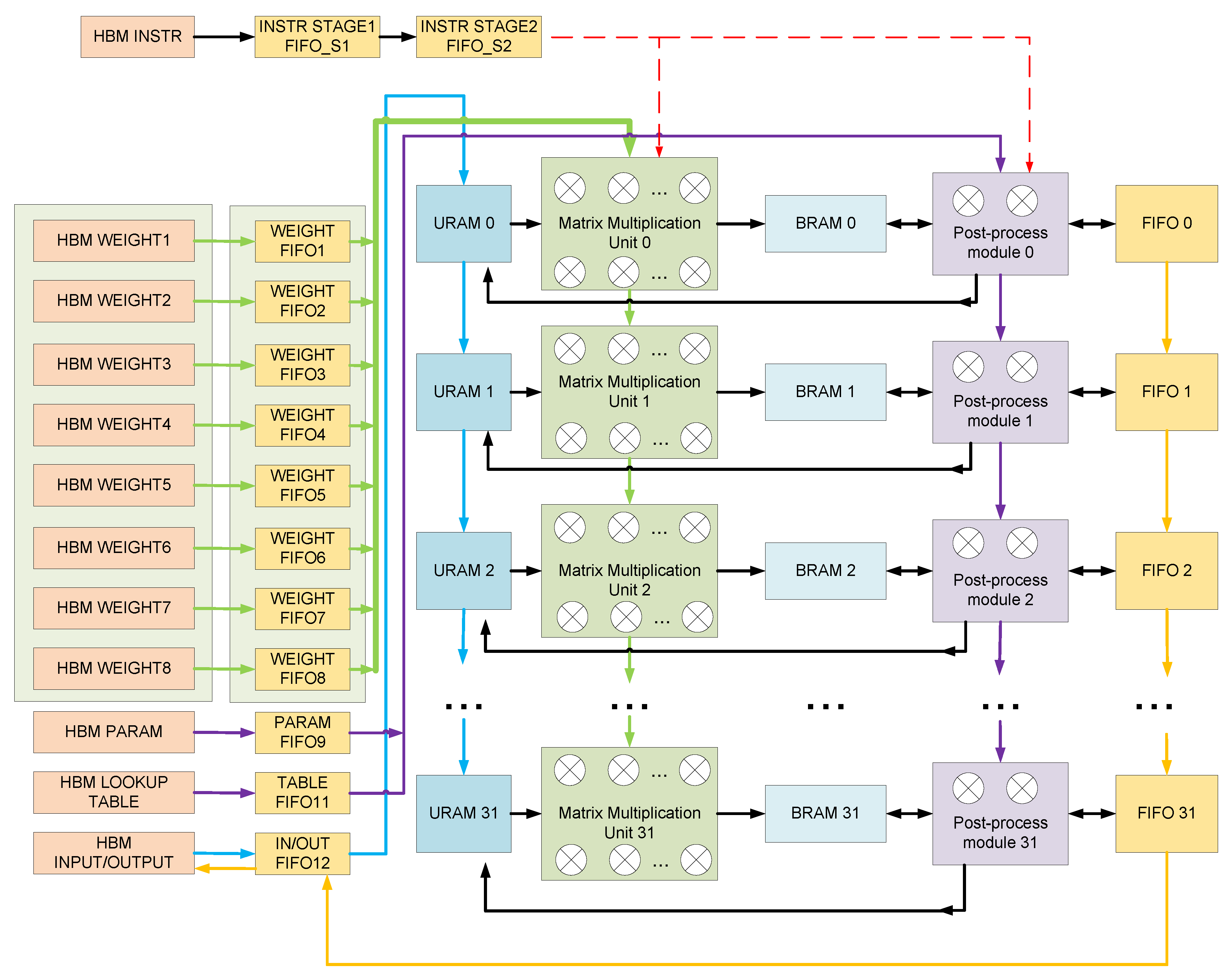
The LSTM is calculated in the kernel, and the kernel in the FPGA completes most of the calculations of the entire system. The following describes the architecture of the kernel, as shown in
Figure 3.
Instructions, weights, post-processing parameters, activation function tables, and input and output data are stored on HBM. Instructions, post-processing parameters and sigmoid tables each take up one HBM. The weight data takes up eight HBMs. The input and output data share an HBM. Inside the computing kernel, each HBM has a corresponding FIFO (first in first out). Each block of HBM uses an AXI interface for data reading and writing. When the kernel starts working, the instruction data are transferred from the HBM to the corresponding FIFO_S1. The state of the command FIFO_S1 is monitored. When the command FIFO_S1 is not empty, the data in the FIFO_S1 will be read and sent to FIFO_S2, and a signal to read data in other HBM will be pulled high. Next, the AXI1 interface to the AXI12 interface will read the data in the HBM, according to the information in the instruction, and transfer it to the corresponding FIFO. At the same time, the data in FIFO12 will be sent to ultra random access memory (URAM), which stores input data and intermediate results.
The calculation of the kernel does not need to wait for all the input data to enter the URAM, and the calculation of the kernel starts when sufficient input data is sent to the URAM. At this time, the instruction enters the kernel from the FIFO_S2, and the matrix multiplication unit will obtain data from the weight FIFO and URAM, according to the information in the instruction for calculation. When the matrix multiplication is finished, the result will be written into the BRAM, and then the post-processing unit will start the calculation. The post-processing unit will obtain the data from FIFO or BRAM, according to the information in the instruction, and obtain the parameters from the FIFO9, storing the parameters for the calculation. Because the two modules write BRAM at different times, the two modules perform calculations simultaneously. After the matrix multiplication unit completes the first set of data calculations, the post-processing unit performs the first set of data calculations and the second set of data enters the matrix multiplication unit.
As shown in
Figure 3, the results calculated by the post-processing unit will be stored in different storage units. Which memory unit is written to, is determined by the information in the instruction. Finally, the data that needs to be written into HBM will be sent to FIFO first and then written into HBM. The proposed batch-based accelerator can process input data from multiple users simultaneously. The input data of multiple users is calculated simultaneously in the kernel, and a total of 32 groups of computing units perform calculations simultaneously. Since the 32 groups of computing units share the same weights and post-processing parameters, the weights and post-processing parameters are transferred between them through cascading. This calculation mode reduces the demand for external HBM storage bandwidth, by reusing weights.
3.3. Design of Matrix Multiplication Unit
Most of the calculations in LSTM are matrix multiplications, and matrix multiplications have the greatest demand for computing resources. We design a matrix multiplication array composed of DSP to perform matrix multiplication. The detailed design of the matrix multiplication unit is shown in
Figure 4 below.
In
Figure 3, we take a 3 × 3 array as an example, and the actual array size is 8 × 8. There are 64 DSPs in total, 8 DSPs in each column as a group. Each group of DSPs calculates the same value in the output matrix. In this calculation mode, the eight groups of DSPs use the same input vector, so the eight groups of DSPs can share the same input vector, through cascading among different groups. This calculation method reduces the bandwidth requirement of the input vector to one-eighth of the calculation mode, without input data sharing. In a matrix multiplication unit, different DSPs use different weights, without using weight sharing. Because each group of eight DSPs computes the same output value, the eight values computed by the eight DSPs are added, to form a partial sum. A complete matrix multiplication operation will be performed multiple times by eight DSPs, and the partial sums obtained from the multiple operations will be accumulated. When a new set of data needs to be calculated, the data input port of the accumulator will be set to zero to perform a new calculation, as shown in
Figure 4.
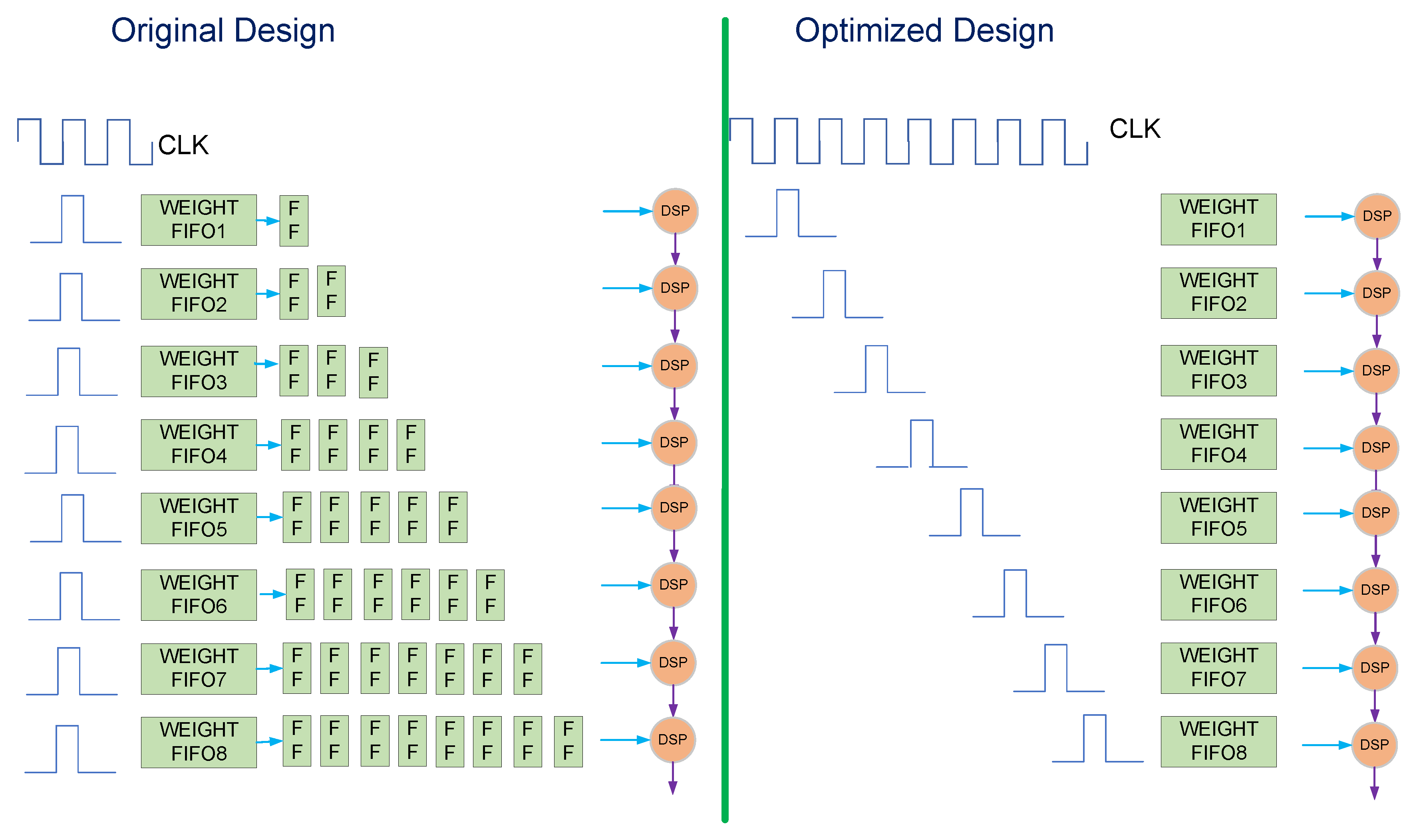
Since different DSPs in a group start calculations at staggered times, the value of the input vector will be registered through registers, and different DSPs in the same group will use different numbers of registers, as shown in
Figure 4. For the reading of weight data, in a common design, the weight is read from the FIFO and then output through a series of registers, as shown in
Figure 5. Since our design has many matrix multiplication units, the weight readout circuit will consume a lot of registers. This may cause difficulties in placement and routing, and result in a relatively low frequency for the final design. In order to reduce the use of registers, we have designed a specific data read timing, as shown in
Figure 5. The read signal arrives at eight different weights, FIFO is staggered. In this mode, each DSP reduces the corresponding 4.5 registers on average. If each data is 16 bits and a matrix multiplication unit has 64 DSPs, then 64 × 16 × 4.5 = 4608 registers can be saved.
3.4. Design of Post-Processing Unit
After the matrix multiplication is completed, the result will be stored in the BRAM, and the post-processing unit will then obtain the data from the BRAM for calculation. The post-processing unit handles all operations except matrix multiplication, including element-wise multiplication, element-wise addition, batch normalization, etc. Although there is no batch normalization operation in LSTM, supporting batch normalization can broaden the applicability of the architecture, so that the accelerator can perform more types of calculations. In particular, in order to simplify the design of the matrix multiplication unit, the addition of bias operation in Equations (
1)–(
5) is also performed in the post-processing unit. In conventional operations, these operations require separate computing resources. Each type of calculation uses a dedicated computing resource. Since these operations are not performed at the same time, this will lead to a waste of computing resources. In order to improve resource utilization, we propose an architecture that utilizes two DSPs to perform all of the above operations. This is achieved through dynamic reconfiguration of the DSP. We make the DSP calculate different operations at different times by changing the operation code when the DSP is running. The detailed structure diagram is shown in
Figure 6.
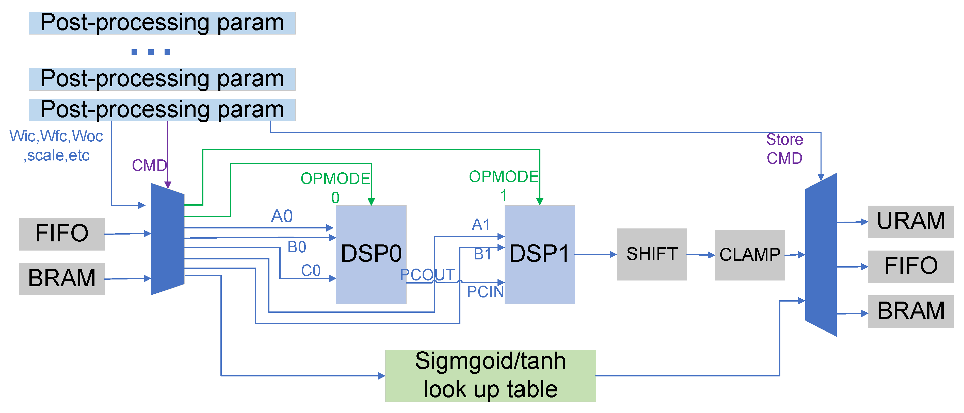
As shown in
Figure 6, the post-processing parameters store the calculation type command, some weights, such as
,
, and the command that determines where the output is stored. Two DSPs are connected by cascading. Firstly, the type of operation performed by the two DSPs is determined by the command word, stored in the post-processing parameters. Different types of operations determine different operation codes. The input data of the two DSPs will be obtained from the BRAM, FIFO, and post-processing parameters through the multiplexer, and which data is to be selected is determined by the operation code. The shift module and the clamp module perform shift operations and truncate values, respectively.
Table 1 illustrates the configuration modes and opcodes of the DSP in different types of operations. Taking the addition of bias in matrix multiplication as an example, in the first stage, we will split the 36 bit data into two input ports A0 and B0 of DSP0, because the output result of matrix multiplication is 36 bit. The bias is placed on the C0 port and the operation completed by DSP0 is
. A colon indicates a bitwise data splicing operation.
represent shift and clamp, respectively. In the second stage, we put
and
on port A0 of DSP0 and port A1 of DSP1, respectively. The quantization parameter scale, representing the ratio between the fixed-point number and the actual floating-point number, is placed on the B ports of the two DSPs. At this time, the operation performed by the two DSPs is
.
Taking batch normalization as an example, data, gamma, and beta are, respectively, placed on ports A0, B0, and C0 of DSP0. In this mode, the operation completed by DSP is
. For element-wise multiplication and element-wise addition, the calculation process is similar. There are two types of element-wise multiplication in
Table 1, which correspond to the two types in the LSTM formula. One type is data multiplied by weights, and the other is data multiplied by data. If these operations are calculated separately, using different DSPs, eight DSPs are required, whereas the proposed architecture reduces the number of DSPs required for these operations to two.
3.5. Design of Sigmoid/Tanh Module
The sigmoid and tanh functions are implemented in our architecture via a lookup table. The values in the lookup table are precomputed in software and loaded into the memory storing the lookup table in advance, before the activation function operation. Using the internal symmetry of the sigmoid function and the tanh function, we only need to store half of the data.
In order to improve the calculation efficiency, and avoid the activation function becoming a bottleneck, we designed a double buffer.
Figure 7 shows a structural diagram of a double buffer that implements an activation function. A double buffer corresponds to a ping-pong operation. One buffer consists of two URAM and the double buffer consists of four URAM. The double buffer stores different lookup tables. For example, one buffer stores the sigmoid table while another buffer stores the tanh table. When the calculation in LSTM is switched from sigmoid to tanh, the data that has been loaded can be used immediately, reducing the time required to load the lookup table.
4. Instruction Design
In
Section 4, we introduce the design details of the instruction set and the execution process of the instruction.
4.1. Information in the Instruction
In our design, the LSTM is split into a sequence of instructions. A matrix multiplication unit calculates eight data at the same time, so each instruction operates on eight data. When the eight data operations performed by one instruction are completed, the next instruction is read in, and the eight data operations of the next instruction are performed. When all instructions finish running, the calculation of the entire network also terminates at the same time. The information contained in an instruction is shown in
Table 2, below.
The instruction contains the following information, information related to the input and output data, information related to the weights, information related to the post-processing parameters, information related to the activation functions, information related to matrix multiplication, information related to FIFO, and storage information about the output data. The functions of the instructions are abundant, which simplifies the design of the state machine of the control module in the hardware circuit. The hardware circuit will read the information from the instruction and decide which data to read for calculation and which address of the memory to store the calculated result, according to the information.
4.2. From LSTM to Instructions
With the network model and instruction definition, an LSTM can be split into a sequence of instructions. The instructions and atomic operations after LSTM decomposition are shown in
Table 3. An atomic operation means an operation that can be completed by a matrix multiplication unit or a post-processing unit at one time.
The seven equations (Equations (
1)–(
7)) are broken down into 24 atomic operations. The 24 atomic operations are completed by a total of five instructions. Which atomic operations each instruction corresponds to, is also shown in
Table 3.
Because matrix multiplication occupies the main amount of the calculation, we use the atomic operation of matrix multiplication as a separation point, to separate the data calculated by each instruction. The operations that can be completed by one instruction, include a matrix multiplication operation and several post-processing operations. For example, instruction 3 performs atomic operations from number 10 to number 16 while instruction 4 performs atomic operations from number 17 to number 23. When instruction 3 is executed, the matrix multiplication unit will perform atomic operation 10. After atomic operation 3 is completed, the post-processing unit will perform the calculation of atomic operation 11 to atomic operation 16, and at the same time, the matrix multiplication unit will perform operations on atomic operation 17. The matrix multiplication unit and the post-processing unit perform calculations simultaneously, which can achieve high throughput and performance. The total amount of instructions is related to the size of the matrix. If the output dimensions of the five matrix multiplications in LSTM are all 1024, and LSTM iterates 32 times, then the total number of instructions is 32 × 1024 × 5/8 = 20,480.
4.3. Memory Reuse during Instruction Execution
During instruction execution, matrix multiplication and post-processing calculations require frequent reading and writing to memory. In order to reduce memory usage and maximize memory utilization, we have designed a memory reuse scheme.
For a matrix multiplication unit, it is relatively simple to read the data from the URAM and write it into the BRAM after calculation, and there is no need to consider memory reuse. For the post-processing unit, because the calculation it performs needs to read and write data repeatedly, we achieve the purpose of reducing storage resources by reusing BRAM, FIFO, and URAM.
Taking atomic operation 4 to atomic operation 9 in
Table 3 as an example, the well-designed data flow is shown in
Table 4.
In order to maximize the use of storage resources, we put multiple data into the same address, by bit width division. As shown in
Table 4, the result of adding bias is placed in BRAM[15:0],
is placed in BRAM [63:48], and the result of element-wise multiplication is placed in BRAM[31:16].
is placed in the FIFO and will be read from the FIFO to participate in the calculation when it needs to be calculated. For other instructions, the operation is similar and will not be repeated here. Through the reuse of storage resources, the intermediate results in all LSTM calculations can be stored on only one BRAM, one URAM, and one FIFO.
5. Experimental Results
5.1. Experimental Setup
In our experiments, we implemented the LSTM network mentioned in
Section 2. Firstly, instructions are generated according to the network structure and hardware structure. The required information, such as data address and length, is stored in the instruction, and the instruction is generated through a Python script. Our accelerator is implemented using Verilog code. Vivado 2020.1 and Vitis 2020.1 are our design development tools.
There are two SLRs (super logic region) on the Xilinx Alevo U50 accelerator card, and we deploy one kernel on each SLR. A kernel is composed of 32 cascaded computing units. Each computing unit consists of a matrix multiplication unit containing 64 DSPs and a post-processing unit containing 2 DSPs. So in our design, there are 64 computing units distributed on two SLRs, which means that the input data of 64 users can be calculated at the same time.
5.2. Resource Utilization
After placing and routing, the resources occupied by the accelerator are shown in
Table 5. The resources used by the platform in
Table 5, are the resources needed by Xilinx FPGA to communicate between the kernel and the host. Through the platform in the FPGA and the Xilinx Runtime (XRT) in the CPU, the host and the kernel can easily transmit data. It can be seen from
Table 5 that 4224 DSPs are used, which is consistent with the result calculated according to the hardware structure. In order to store input data and intermediate results, the usage of URAM and BRAM in our design is within an acceptable range. The usage of BRAM is 282 through our resource reuse, otherwise more BRAM would be used. The kernel uses 122,935 lookup tables (LUTs), mainly because the instruction-driven design reduces the complexity of the hardware design. If the control module is not implemented by instructions, more LUTs will be required than in the current design. The usage of registers is slightly larger, mainly due to the cascaded design, which needs to register a lot of data.
5.3. Performance Comparison
We compared our results with those of others. Since we have not seen work implementing LSTM using the same Alevo U50 card, we compare it with work using FPGAs with a similar amount of computational resources. The comparison results are in
Table 6.
In our design, the overall circuit runs at 280 MHz. Our accelerator achieves a performance of 2036 GOPS at a 16-bit data bit width. The power consumption of our design, in
Table 6, is obtained through Xilinx’s power analysis tool. Compared with the work in [
9], our design has higher performance and resource utilization, while using the same 16 bit data precision. Compared with the work in [
16,
18], our performance is lower but the data bit width used in [
16,
18] is 8 bit. Because there are rich int8 multipliers in Stratix 10 GX2800, int8 performance will be relatively high in Stratix 10 GX2800. Our design has higher resource utilization compared to [
16,
18]. Compared with [
6,
22], we obtain higher performance with higher data precision. Due to the simultaneous computation of data for 64 users, our design occupies a relatively large on-chip storage space (14.74 MB) and has a higher latency than other works. On the one hand, because the instructions in our design are executed continuously, the DSP in the matrix multiplication unit has almost no idle time and operates continuously. On the other hand, because the DSP of the matrix multiplication unit and the DSP of the post-processing unit work in parallel, and the DSP of the post-processing unit realizes different operations by configuring different modes, the hardware utilization of our work reached 86.1%, which exceeds the current designs.
6. Conclusions
This paper presents an instruction-driven LSTM accelerator. The hardware part of the accelerator consists of a matrix multiplication unit and a post-processing unit. The matrix multiplication unit adopts a staggered reading scheme in the weight reading stage, to reduce the consumption of register resources. The post-processing unit completes operations such as element-wise multiplication, element-wise addition, batch normalization, and bias addition, by using only two DSPs, through resource sharing. Multi-layer LSTM and large LSTM can be decomposed into a series of instructions for execution, each of which executes a certain amount of data. Our design is implemented on the Xilinx Alevo U50 card, and the experimental results show that our design can achieve 2036 GOPS performance, and the resource utilization of hardware exceeds the existing designs. Our design currently uses 16-bit data and will support optimization of low-bit precision data in future work. Using low-bit data, such as 8-bit data, can further enhance the overall performance. Our research can be used in scenarios such as speech recognition and machine translation, in the data center.
Author Contributions
Conceptualization, N.M., H.Y. and Z.H.; methodology, N.M., H.Y. and Z.H.; software, N.M.; validation, N.M.; investigation, N.M., H.Y. and Z.H.; writing—original draft preparation, N.M.; writing—review and editing, N.M., H.Y. and Z.H.; supervision, H.Y.; project administration, H.Y.; funding acquisition, H.Y. All authors have read and agreed to the published version of the manuscript.
Funding
This work was supported by the National Natural Science Foundation of China, under grant 61876172.
Conflicts of Interest
The authors declare no conflict of interest.
References
- Amodei, D.; Ananthanarayanan, S.; Anubhai, R.; Bai, J.; Battenberg, E.; Case, C.; Casper, J.; Catanzaro, B.; Cheng, Q.; Chen, G.; et al. Deep Speech 2: End-to-End Speech Recognition in English and Mandarin. In Proceedings of the 33rd International Conference on Machine Learning, New York, NY, USA, 19–24 June 2016; pp. 173–182. [Google Scholar]
- Jouppi, N.P.; Hyun Yoon, D.; Ashcraft, M.; Gottscho, M.; Jablin, T.B.; Kurian, G.; Laudon, J.; Li, S.; Ma, P.; Ma, X.; et al. Ten Lessons From Three Generations Shaped Google’s TPUv4i: Industrial Product. In Proceedings of the 2021 ACM/IEEE 48th Annual International Symposium on Computer Architecture (ISCA), Valencia, Spain, 14–18 June 2021; pp. 1–14. [Google Scholar]
- Rybalkin, V.; Sudarshan, C.; Weis, C.; Lappas, J.; Wehn, N.; Cheng, L. Efficient Hardware Architectures for 1D- and MD-LSTM Networks. J. Signal Process. Syst. 2020, 92, 1219–1245. [Google Scholar] [CrossRef]
- Que, Z.; Zhu, Y.; Fan, H.; Meng, J.; Niu, X.; Luk, W. Mapping Large LSTMs to FPGAs with Weight Reuse. J. Signal Process. Syst. 2020, 92, 965–979. [Google Scholar] [CrossRef]
- Azari, E.; Vrudhula, S. An Energy-Efficient Reconfigurable LSTM Accelerator for Natural Language Processing. In Proceedings of the 2019 IEEE International Conference on Big Data (Big Data), Los Angeles, CA, USA, 9–12 December 2019; pp. 4450–4459. [Google Scholar]
- Liu, M.; Yin, M.; Han, K.; DeMara, R.F.; Yuan, B.; Bai, Y. Algorithm and hardware co-design co-optimization framework for LSTM accelerator using quantized fully decomposed tensor train. Internet Things 2023, 22, 100680. [Google Scholar] [CrossRef]
- Que, Z.; Nakahara, H.; Nurvitadhi, E.; Boutros, A.; Fan, H.; Zeng, C.; Meng, J.; Tsoi, K.H.; Niu, X.; Luk, W. Recurrent Neural Networks With Column-Wise Matrix–Vector Multiplication on FPGAs. IEEE Trans. Very Large Scale Integr. (VLSI) Syst. 2022, 30, 227–237. [Google Scholar] [CrossRef]
- Que, Z.; Wang, E.; Marikar, U.; Moreno, E.; Ngadiuba, J.; Javed, H.; Borzyszkowski, B.; Aarrestad, T.; Loncar, V.; Summers, S.; et al. Accelerating Recurrent Neural Networks for Gravitational Wave Experiments. In Proceedings of the 2021 IEEE 32nd International Conference on Application-specific Systems, Architectures and Processors (ASAP), Piscataway, NJ, USA, 7–9 July 2021; pp. 117–124. [Google Scholar]
- Wang, S.; Li, Z.; Ding, C.; Yuan, B.; Qiu, Q.; Wang, Y.; Liang, Y. C-LSTM: Enabling Efficient LSTM using Structured Compression Techniques on FPGAs. In Proceedings of the 2018 ACM/SIGDA International Symposium on Field-Programmable Gate Arrays, Monterey, CA, USA, 25–27 February 2018; pp. 11–20. [Google Scholar]
- Azari, E.; Vrudhula, S. ELSA: A Throughput-Optimized Design of an LSTM Accelerator for Energy-Constrained Devices. ACM Trans. Embed. Comput. Syst. 2020, 19, 3. [Google Scholar]
- Cao, S.; Zhang, C.; Yao, Z.; Xiao, W.; Nie, L.; Zhan, D.; Liu, Y.; Wu, M.; Zhang, L. Efficient and Effective Sparse LSTM on FPGA with Bank-Balanced Sparsity. In Proceedings of the 2019 ACM/SIGDA International Symposium on Field-Programmable Gate Arrays, Seaside, CA, USA, 24–26 February 2019; pp. 63–72. [Google Scholar]
- Chen, J.; Hong, S.; He, W.; Moon, J.; Jun, S.-W. Eciton: Very Low-Power LSTM Neural Network Accelerator for Predictive Maintenance at the Edge. In Proceedings of the 2021 31st International Conference on Field-Programmable Logic and Applications (FPL), Dresden, Germany, 30 August–3 September 2021; pp. 1–8. [Google Scholar]
- Ioannou, L.; Fahmy, S.A. Streaming Overlay Architecture for Lightweight LSTM Computation on FPGA SoCs. ACM Trans. Reconfigurable Technol. Syst. 2022, 16, 8. [Google Scholar] [CrossRef]
- Kim, T.; Ahn, D.; Lee, D.; Kim, J.-J. V-LSTM: An Efficient LSTM Accelerator using Fixed Nonzero-Ratio Viterbi-Based Pruning. IEEE Trans. Comput.-Aided Des. Integr. Circuits Syst. 2023, 1. [Google Scholar] [CrossRef]
- Nurvitadhi, E.; Kwon, D.; Jafari, A.; Boutros, A.; Sim, J.; Tomson, P.; Sumbul, H.; Chen, G.; Knag, P.; Kumar, R.; et al. Why Compete When You Can Work Together: FPGA-ASIC Integration for Persistent RNNs. In Proceedings of the 2019 IEEE 27th Annual International Symposium on Field-Programmable Custom Computing Machines (FCCM), San Diego, CA, USA, 28 April–1 May 2019; pp. 199–207. [Google Scholar]
- Que, Z.; Nakahara, H.; Fan, H.; Li, H.; Meng, J.; Tsoi, K.H.; Niu, X.; Nurvitadhi, E.; Luk, W. Remarn: A Reconfigurable Multi-threaded Multi-core Accelerator for Recurrent Neural Networks. ACM Trans. Reconfigurable Technol. Syst. 2022, 16, 4. [Google Scholar] [CrossRef]
- Que, Z.; Nakahara, H.; Fan, H.; Meng, J.; Tsoi, K.H.; Niu, X.; Nurvitadhi, E.; Luk, W. A Reconfigurable Multithreaded Accelerator for Recurrent Neural Networks. In Proceedings of the 2020 International Conference on Field-Programmable Technology (ICFPT), Maui, HI, USA, 9–11 December 2020; pp. 20–28. [Google Scholar]
- Que, Z.; Nakahara, H.; Nurvitadhi, E.; Fan, H.; Zeng, C.; Meng, J.; Niu, X.; Luk, W. Optimizing Reconfigurable Recurrent Neural Networks. In Proceedings of the 2020 IEEE 28th Annual International Symposium on Field-Programmable Custom Computing Machines (FCCM), Fayetteville, AR, USA, 3–6 May 2020; pp. 10–18. [Google Scholar]
- Que, Z.; Nugent, T.; Liu, S.; Tian, L.; Niu, X.; Zhu, Y.; Luk, W. Efficient Weight Reuse for Large LSTMs. In Proceedings of the 2019 IEEE 30th International Conference on Application-specific Systems, Architectures and Processors (ASAP), New York, NY, USA, 15–17 July 2019; pp. 17–24. [Google Scholar]
- Rybalkin, V.; Ney, J.; Tekleyohannes, M.K.; Wehn, N. When Massive GPU Parallelism Ain’t Enough: A Novel Hardware Architecture of 2D-LSTM Neural Network. ACM Trans. Reconfigurable Technol. Syst. 2021, 15, 2. [Google Scholar]
- Rybalkin, V.; Pappalardo, A.; Ghaffar, M.M.; Gambardella, G.; Wehn, N.; Blott, M. FINN-L: Library Extensions and Design Trade-Off Analysis for Variable Precision LSTM Networks on FPGAs. In Proceedings of the 2018 28th International Conference on Field Programmable Logic and Applications (FPL), Dublin, Ireland, 27–31 August 2018; pp. 89–96. [Google Scholar]
- Jiang, J.; Xiao, T.; Xu, J.; Wen, D.; Gao, L.; Dou, Y. A low-latency LSTM accelerator using balanced sparsity based on FPGA. Microprocess. Microsystems 2022, 89, 104417. [Google Scholar] [CrossRef]
- He, D.; He, J.; Liu, J.; Yang, J.; Yan, Q.; Yang, Y. An FPGA-Based LSTM Acceleration Engine for Deep Learning Frameworks. Electronics 2021, 10, 681. [Google Scholar] [CrossRef]
- Hochreiter, S.; Schmidhuber, J. Long Short-Term Memory. Neural Comput. 1997, 9, 1735–1780. [Google Scholar] [CrossRef] [PubMed]
- Sak, H.; Senior, A.; Françoise, B. Long short-term memory recurrent neural network architectures for large scale acoustic modeling. In Proceedings of the 15th Annual Conference of the International Speech Communication Association, Singapore, 14–18 September 2014; pp. 338–342. [Google Scholar]
| Disclaimer/Publisher’s Note: The statements, opinions and data contained in all publications are solely those of the individual author(s) and contributor(s) and not of MDPI and/or the editor(s). MDPI and/or the editor(s) disclaim responsibility for any injury to people or property resulting from any ideas, methods, instructions or products referred to in the content. |
© 2023 by the authors. Licensee MDPI, Basel, Switzerland. This article is an open access article distributed under the terms and conditions of the Creative Commons Attribution (CC BY) license (https://creativecommons.org/licenses/by/4.0/).


