Article

Design and Implementation of CNFET SRAM Cells by Using Multi-Threshold Technique

1
Electronics and Communication Engineering, M.Kumarasamy College of Engineering, Karur 639 113, India
2
Electrical and Electronics Engineering, M.Kumarasamy College of Engineering, Karur 639 113, India
3
Electromechanics Engineering Department, Faculty of Engineering, Heliopolis University, Cairo 11785, Egypt
4
Department of Mechanical Engineering, Faculty of Engineering, ‘Dunarea de Jos’ University of Galati, 6200 Galati, Romania
*
Author to whom correspondence should be addressed.
Electronics 2023, 12(7), 1611; https://doi.org/10.3390/electronics12071611
Submission received: 29 December 2022 / Revised: 9 March 2023 / Accepted: 27 March 2023 / Published: 29 March 2023

Abstract

:
This paper presents a CNFET (Carbon Nano-tube FET) based MT (Multi-Threshold)-SRAM (Static Random Access Memory) design based on the leakage reduction mechanism. A multi-threshold logic is employed for reducing the leakage current during read/write operations. Here, the multi-threshold technique is used to insert the high threshold sleep control to the low threshold circuit. The insertion is performed in a serial manner. The high threshold transistors are very useful for deriving the low sub-threshold current. Meanwhile, the low threshold transistors are promising for improving the circuit performance. The high-low threshold transistor pairs are used to change the channel length by modifying the oxide thickness of the transistors. The overall implementation of the Multi-threshold-based SRAM cells are implemented with the help of CNFET in-order to avoid the short channel effect, mobility degradation which is occurred while considering the channel length below 32 nm in CMOS (Complementary Metal Oxide Semiconductor) devices. The paper clearly represents the performance improvement of the proposed SRAM cells with above-mentioned technologies.

1. Introduction

In many electronic devices and microprocessors, the SRAM (Static Random Access Memory) is commonly used for caches. The SRAM produced better performance compared with the Dynamic Random Access Memory (DRAM). The DRAM capacity is much greater than the static type and it needs more time to refresh itself. This time delay causes the increment of the latency to access the data. In recent electronic devices that are assigned for particular applications such as multimedia, object tracking, video processing, and medicine, the computation process and complexity have been increased and it is also reflected in the power consumption. These devices have unique processors that consumed huge SRAM sub-modules. Hence, the SRAM is one of the much delegated memory modules for power considerations [1]. The limitation of the SRAM power consumption is performed by decreasing Vdd supply voltage or Vth threshold voltage.

1.1. Basics of CNFET

At nano-meter region of channel length, the CMOS devices will achieve the technological physical limitations. Due to this physical limitation, the failure and defect rate to be much huge in MOSFET devices. Therefore, an emerging developed technology is required to achieve the high performance. Hence, the CNFET is one of the most promising technologies instead of Si-based devices. The reason for taking the CNFET devices over the silicon devices can be justified by,
(1)
Effect of Gate oxide thickness: If the gate oxide thickness of CMOS devices decreases, it will increase the quantum capacitance for a variety of gate voltages.
(2)
Effect of Temperature: The CMOS behavior and characteristics change with respect to the increase in the temperature rating. The acceptable temperature rating of the Si-CMOS device is 150°. This temperature rating severely affects the Vth (threshold voltage). For example, if the temperature increases from 27° to 227°, it will vary the 4.6% variation of the Vth. In this case, we definitely stated that the CMOS operates maximum at 150° and device parameter changed at high temperature rate.
(3)
Effect of Channel Length (Lch): Channel length is the key factor in CMOS devices. If we are decreasing the channel length, it will reflect in the changes in the packing density. As the channel length of CMOS devices scales down to the nano-meter region, the Vth was also scaled and it will increase the leakage power. The increases in the leakage power bring changes in leakage current, which becomes the limiting factor of thinner oxide thickness of 1.5 nm. If the Lch becomes very less, the drain depletion region will enter the source and it will decrease the e- injection barrier. It automatically degrades the device performance.
(4)
Parameter consideration of CMOS & CNFET: Both devices have unique parameter specifications in circuit design. The following Table 1 illustrates the parameter variation of the CMOS and CNFETs.
The CMOS-based SRAM cells suffered from short channel effects (SCEs), mobility degradation, etc. when considering the channel length of 32 nm. Hence, the CMOS devices did not produce better performance in 32 nm channel length. This drawback was overcome by introducing the multi-gate devices such as Fin-FET and CNFET.
In recent decades, the CNTs have more attention because of its thermal, electrical and mechanical properties. Based on the ultra long mean-free path, the CNFETs are classified for elastic scattering, which is similar for holes, electrons, easy combination of high-K dielectric materials, and high Fermi velocity characteristics. The fabrication process of the CMOS and CNFET is similar, and the design approaches of CMOS are separated for CNFET based circuit design. Due to the huge current drive capability, less PDP (Power Delay Product), high thermal stability and ballistic transport, the CNFETs have been considered promising devices [2]. 
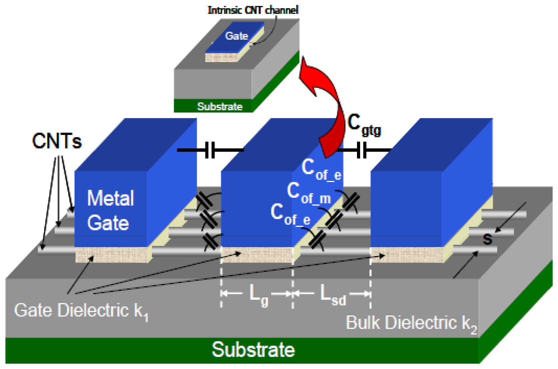
Figure 1 shows the layouts of the CNFET where the channel regions are highly doped and less dopant are added to the CNT channel. These are considered the interconnection between the 2 adjacent devices or S/D extended region. The single intrinsic CNT (inset) model is depicted in Figure 1, which is the origin point of the modeling of complete CNFET devices [3].
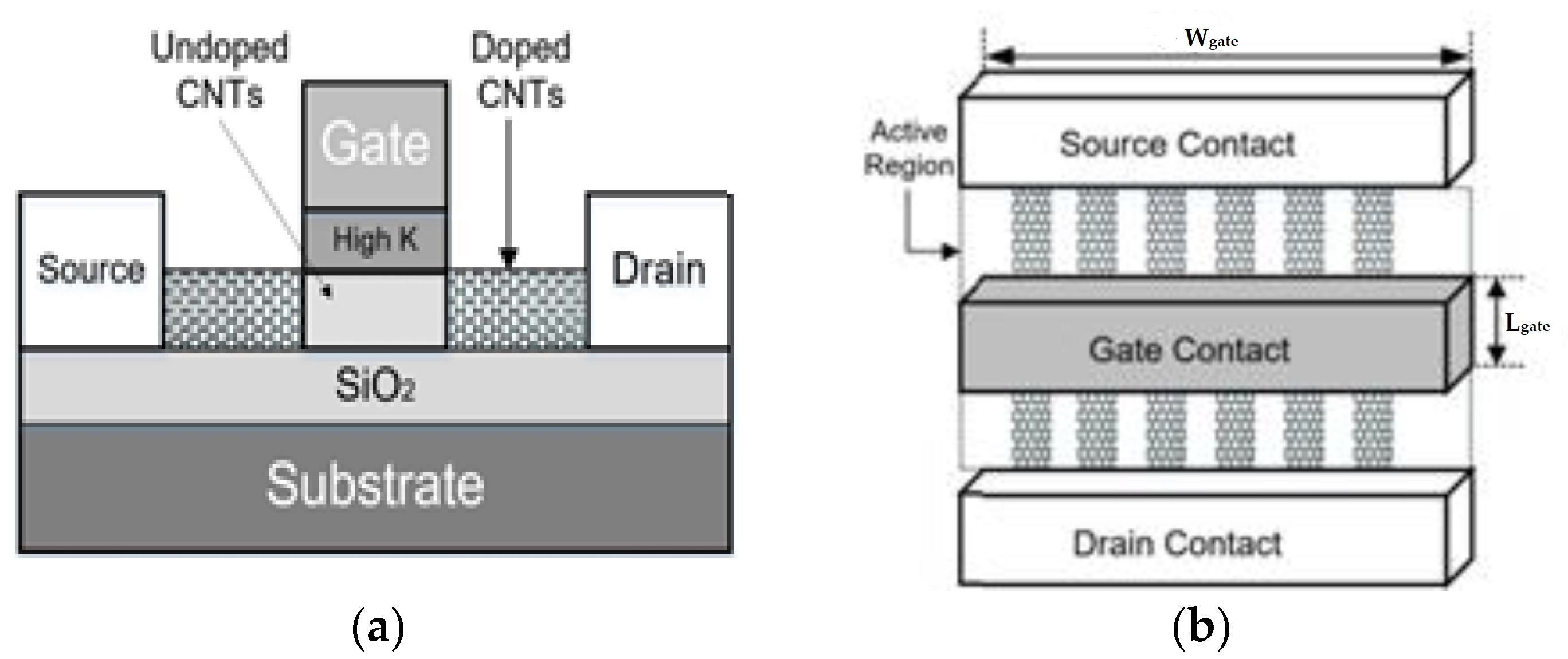
Figure 2a,b show the CNFET’s side and top view, which consist of 6 single walled CNTs considered as the channel material. The CNT is either a semiconducting or metallic material based on the chirality factor. The recent CNFETs give considerable percentage for metallic CNTs (m-CNTs), which short the S/D in CNFETs. This m-CNT is removed by employing the proper function. Here, two important methods incorporated to neglect the unwanted m-CNTs, (1) SCE (Selective Chemical Etching) and (2) VMR (VLSI compatible m-CNT Removal). The above-mentioned two methods eliminate the metallic tube, which is close to 99.9%. A traditional synthesis process of CNFETs approximately produced 113 m-CNT and 2/3 s-CNT (semiconducting CNTs). In recent CNT, growth methodologies reach high amounts (90%) of producing s-CNTs [4]. However, there is no technique available for achieving 100% CNT-growth. Hence, it is an important for adapting the different techniques for removing the m-CNTs like chemical etching process and electrical burning, etc. At the same time, the diameter variation of the CNTs affects the electrical properties such as threshold voltage and drive current. The multiple diameter distribution and mean diameters are observed based on the CNTs production method. During the manufacturing process of the CNFETs, these variations occurred due to doping process and mis-positioned/mis-aligned CNTs in the transistor. This leads to short the CNFETs. However, to date, the CNFETs didn’t include this type of source variability [5].
The initial stage of the CNFET fabrication involves the parallel metal strips pre-patterning in SiO2 substrate. Once the pre-patterning process is completed, CNTs are deposited at the top in a random manner. This CNTs fall around the two metal strips and meet all necessary requirements for basic FET. Here, one metal for the source terminal and another for the drain terminal. The source/drain terminals are made from the chromium/gold materials and SiO2 is used as the gate oxide.

1.2. CNFET Parameters

(1)
CNTs Array: CNT is the hollow nature of a nano-structured cylinder which is made from the carbon atoms. The CNTs have a mono-shell of carbon atoms known as SWCNTs (single-walled CNTs). The CNFET is different from the MOSFET in that it contains the channels built with a parallel of CNTs arrays [2].
(2)
Diameter: The CNFET’s diameter is defined by the chirality factor (n, m) where n and m are non-negative integers. Based on (n, m), the nature of the CNFET is defined as either metallic or semiconductor. If we are considering diameter as 1.5 nm, then the chirality factor is equal to (19, 0) [6].
(3)
Technology Parameters: The specification of the technology parameters for 32 nm channel length is described in Table 2.

1.3. Existing Methodologies of Designing SRAM Cells

In recent decades, several methodologies boomed for efficient designing of SRAM cells. A high-speed 10T SRAM cell was developed by [7] in FinFET technology at 14 nm channel length. The presented 10T-SRAM cell was approximately 2 times greater than the Six-Transistor HD SRAM cell. Next to this, a low leakage SRAM cell was designed by [8] in which the memory cells were based on the S (Source)-biased inverter. Additionally, two transistors were used in the S-biased inverter to diminish the Ileakage current, which results in saving of leakage power up-to 67% when compared with the traditional inverter. The double ended low powers SRAM was constructed by ref. [9], which utilize the low-power stacked inverters for limiting the power dissipation. By introducing cross-coupled inverters with low Vdd, the power dissipation is further reduced in the hold mode with power gating techniques.
A low-power single-ended 9T SRAM cell was designed by ref. [10], which countered against LPA and discussed the issue of leakage balance. 7 nm FinFET-based 6T SRAM cell was designed by [11] and the performance comparison was completed with different FinFET devices such as PU (Pull-Up): PD (Pull Down): PG (Pass Gate) transistor ratios to come out suitable devices for LP (low power) and HS (high speed) SRAM applications. The HP SRAM cell was constructed by ref. [12] by using the array of high-bandwidth with 0.0300-μm Intel 4 CMOS technology. The presented 6T SRAM array was compared with 8T SRAM cell for the applications of high-bandwidth memories. By using the 12 nm FinFET technology, the researcher [13] designed an SRAM cell with six transistors. Here, Static Noise Margin (SNM) was used to determine the SRAM cell’s stability.
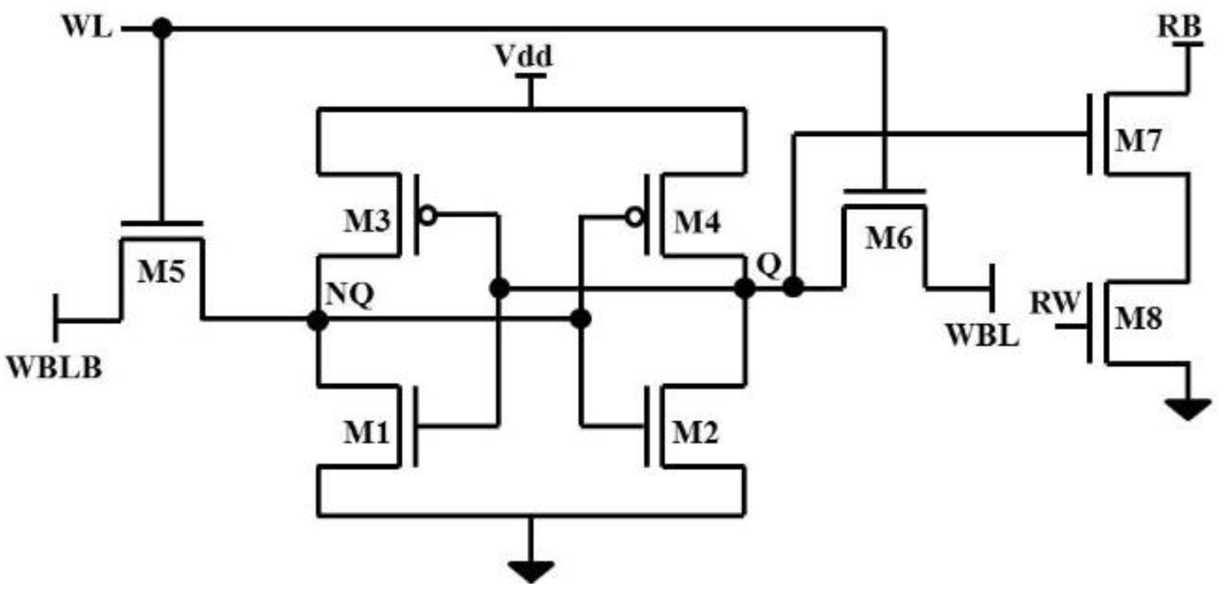
The 8T SRAM cell was designed using a pair of PMOS/NMOS transistors as a diode connection in-order to limit the leakage current [14]. This architecture controlled the amplitude of the current. As Fin-FET devices gave lower Vth which is much superior to the gate leakage. The diode-linked NMOS-PMOS was employed to achieve B-S (Bulk-Source) difference to limit the sub-threshold and gate leakages. The diode connected Multiple approaches were utilized for reducing the leakage current. Meanwhile, the amount of leakage power was reduced and increased the performance. The leakage power reduction on SRAM cells is presented by ref. [15]. Here, the authors performed the dual voltage assignment for reducing the leakage power effectively. On the other hand, the memristor based SRAM cell was designed by [16]. Here, the memristor is mainly used for reducing the area consumption compared with the CMOS design without negotiating the functionality of the device. The noise margin was improved in the 7T SRAM cell which had the channel length of 7 nm. By incorporating the technologies like sleep transistors, DTMOS, and MOSFET, the 7T SRAM were designed and also performance analysis was also completed in this method [17].
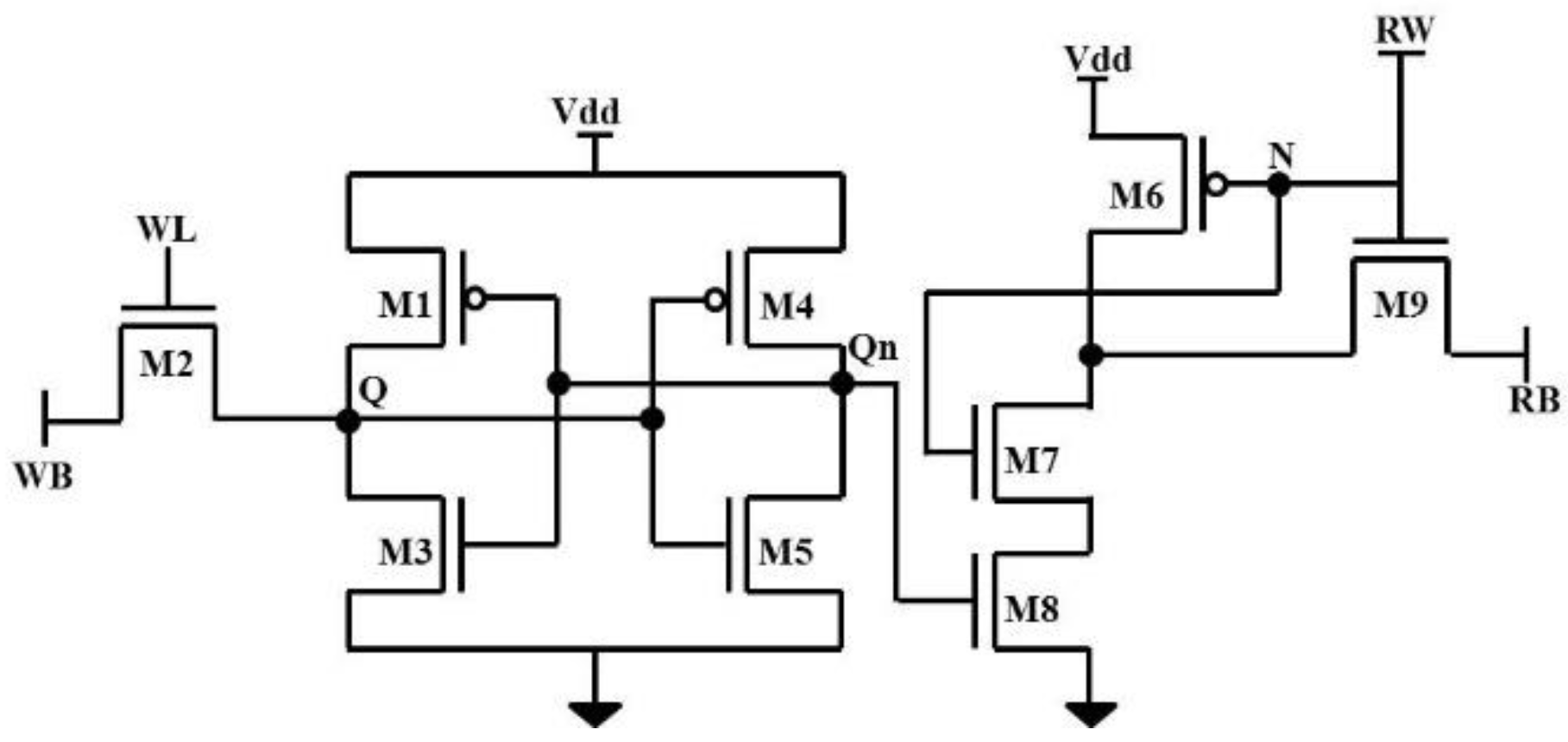
Dual-rail SRAM with embedded level shifting was designed by [18]. This method was mainly implemented to enhance the dual-rail SRAM’s availability because it had more potential to increase demand in low power applications. At low supply voltage, there was a huge degradation in performance, which couldn’t satisfy the high-performance cache necessity in modern computers. The author designed the 6T SRAM based on a comprehensive assessment in 7 nm FinFET technology. Here, the circuit implementation was completed by quantum physics-based device co-optimization. The power gating based FinFET SRAMs were developed by [19] and the method contained three techniques for minimizing the EDP (Energy-Delay Product) and leakage power of 8T and 6T SRAM cells [20].
In recent years, CNFET (Carbon Nano-tube Field Effect Transistor) technology-based circuit design has been raised enormously. The author [21] designed the CNFET-based SRAM cell. The presented design was optimized on the basis of trades such as power efficiency, stability, and performance. The ternary-based two SRAMs were designed by ref. [22], which contain different technologies. In the initial design, the cyclic operation was completed in ternary logic, with a secondary design based on the buffer that was mainly employed for the ternary inverters in both positive and negative cycles.
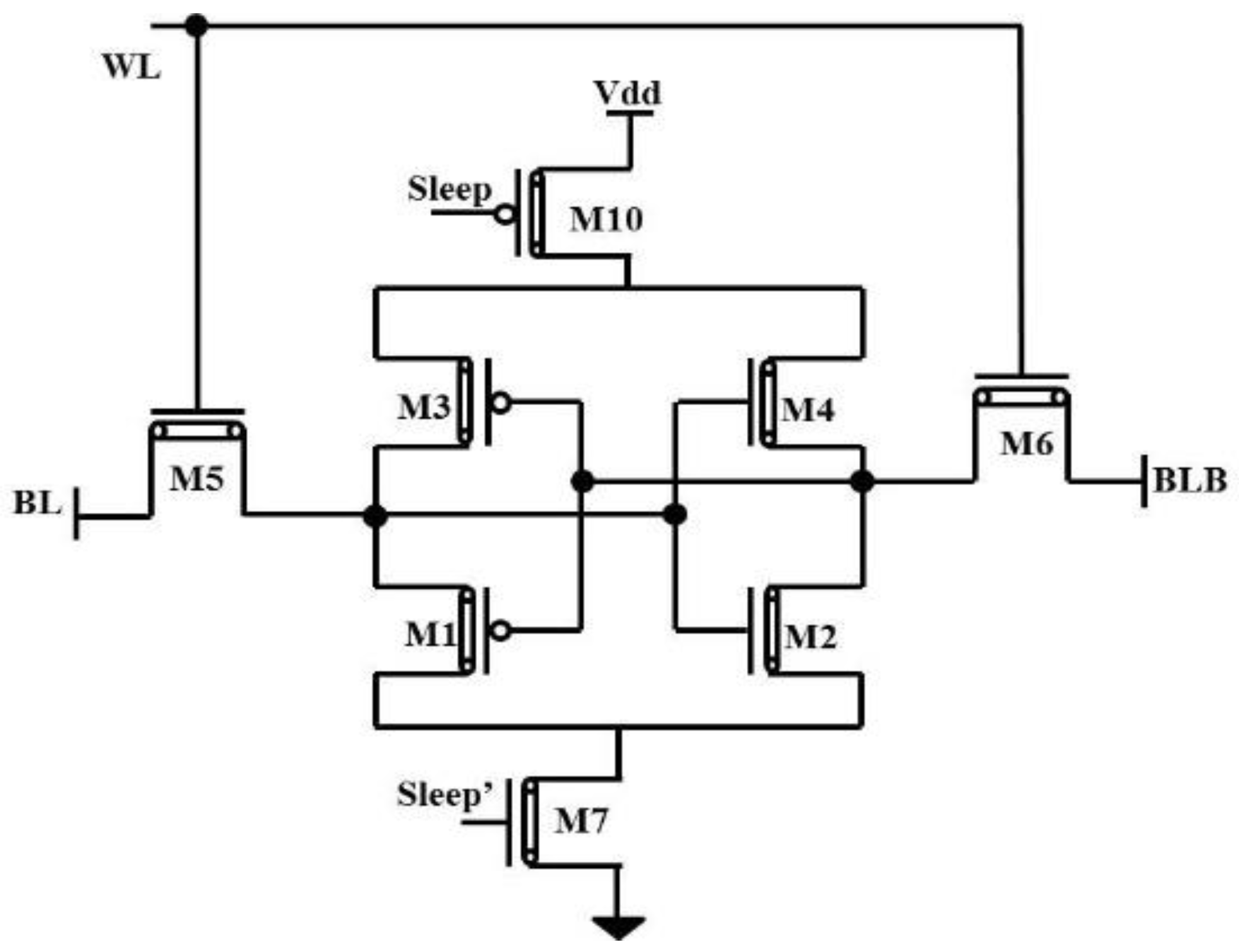
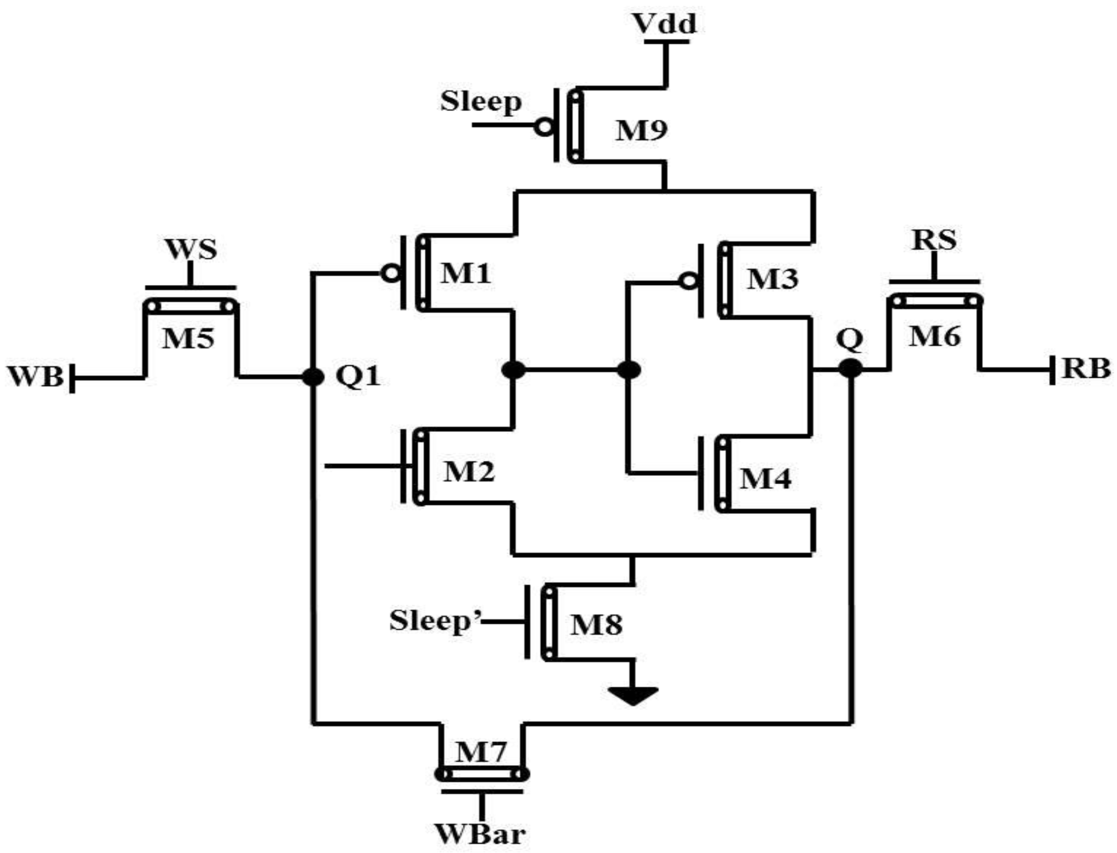
As we summarized, the previous SRAM cells suffered from leakage. Hence, multi-threshold logic is one of an existing and innovative methodology that uses the low-threshold transistor for designing the circuits. This helps to improve the performance of the circuit in active mode and saves leakage power in the standby mode. Due to ambi-polar properties, there is a possibility of leakage in the CNFET devices. So, this special logic (i.e.,) Multi-Threshold (MT) logic is influenced by the CNFET to reduce leakage while considering the 32 nm channel length of the SRAM cell design.

1.4. Importance of Multi-Threshold (MT) Logic

In VLSI, the power reduction and leakage reduction [23] are mainly aimed at producing the circuit to be more efficient. This power reduction is very important to meet the desired temperature characteristics, increase battery life time for compact devices and reduce the cost of packaging and maintenance.
Multi-Threshold (MT) is also known as the power gating technique, which provides efficient and simple power gating logic by using the low threshold voltage and high-speed transistors for constructing the logic cells and uses the high threshold voltage and less leakage devices as sleep transistors. This sleep transistor (ST) provides higher resistance between the Vdd and ground to minimize leakage dissipation. The STs are controlled with the help of sleep control signals. When sleep = 1, the ST in switched OFF during the standby mode which causes the limiting of leakage by ST. The entire leakage of the circuit is limited by the ST’s high threshold voltage. During active mode, the sleep signal in ‘0’ state and provides the connection between the real to virtual ground. As a result of this connection, the lower threshold logic gates operate in very high speed. In this active mode, the STs are working like a resistor.

2. Traditional SRAM Cells

2.1. 6T-SRAM Cell

A collection of 6-transistors, along with a sense amplifier, write circuitry, and row and column decoders are used to construct the conventional SRAM cell, and its schematic view is depicted in the Figure 3 [24].
Read Operation: SRAM cell addresses are decoded by the column and row decoders in which the data has to be read. Initially, the BL is pre-charged to V before the read operation starts. Once the word line (WL) is activated, the B is discharged via the M5 transistor. The voltage variation in the BL is very small due to the limited capability of the cell driving current. The small voltage difference across BLs is sensed by the sense amplifier, and finally, whether the value “1” or “0” is stored in the SRAM cell.
Write Operation: with the help of the external devices, the data has to be stored. The column-row decoders are used for providing the address of the cell. When the WL is enabled, the write function is processed to write the data into the cell, which is fully dependent on the column gate condition. The amount of time consumed by the write operation is less when compared with the reading operation time because the write buffer has a high capability to drive the huge driving current.

2.2. 7T-SRAM Cell

The 7T-SRAM cell is mainly considered for reducing the static power and improvising the read operation. Here, the transistor M7 is connected to form the feedback mechanism in order to boost the high value at the primary inverter and lower value on the secondary inverter, and vice-versa. The read and write operations are performed by M5 and M6 transistors by enabling WS and RS signals, respectively. During the read cycle, the M7 transistor is in ON condition and M7 is OFF in write operation. By resizing the M6 and M7 transistors, the performance of the read cycles is improvised, and the charging of the RB (Read Bit-line) becomes faster. The 7T-SRAM cell configuration is illustrated in Figure 4 [24,25].

2.3. 8T-SRAM Cell

Figure 5 illustrates the schematic view of an 8T-SRAM cell. The structure of the 8T-SRAM cell looks like a 6T SRAM cell in which additional 2 transistors are used for separating the internal inverter and WL during read cycle operation. Before initialization of read operation, the RB is pre-charged to the supply voltage Vdd. Here, the read cycle is enabled by bit RW whereas RB remains in either logic 1 or logic 0 states, which depends on the Q internal node. The write cycle of the 8T-SRAM is similar to the 6T-SRAM write operation [24].

2.4. 9T-SRAM Cell

The pairs M4–M5 and M1–M3 are used for constructing the internal inverters, whereas one bit information is stored as illustrated in Figure 6. With the aid of WB and transistor M2, the write cycle has been performed. Meanwhile, the bit RB and transistors M6, M7, and M8 are utilized for performing the read cycle. Due to 9T structure, the read cycle data stability has been significantly improved [24].

2.5. Difference between 6T, 7T, 8T and 9T SRAM Cells

The stated 6T, 7T, 8T, and 9T SRAM cells are uniquely designed for particular reason.
  • In 6T SRAM cell, the transistor pairs (M1–M3 and M2–M4) are used to form the inverters. In this structure, these transistor pair employed to store the information of bits. The transistors M5 and M6 called as access transistors for performing read and write operations. By selecting, dual bit-lines, the noise margin can be improved.
  • In 7T SRAM Cell, an additional feedback transistor is employed for improving the read and write cycle and it also reduces the static power consumption.
  • In 8T SRAM Cell, an additional two transistors are used for isolating the inverter pairs from accidental write operation while performing read operation. It produces high noise margin compared with the 6T SRAM Cell.
  • During Read cycle of 9T SRAM Cell, the data stability is improved when compared with other SRAM cells.

3. Proposed Multi-Threshold SRAM Cells

3.1. Mathematical Modeling of MT-Logic

A sleep transistor (ST) is either N-type or P-type, and it is mainly employed to shut off or switch on the power supplies to design parts in standby mode. Generally, the P-type ST is used to switch on the Vdd supply, and hence is known as a “Header switch”. The N-type ST normally controls the Vss supply, so it is known as “Footer switch”. The approach of the ST is straight forward; the optimized design of the ST is a challenge due to various effects, such as performance, routability, entire power dissipation, area, and signal/power integrity.
The high quality of the ST design is justified by three important metrics, such as efficiency of the area, IR drop, and switch efficiency. The ST can be optimized in terms of gate length, width, and body bias, and finger size in order to achieve a high amount of area and switching efficiency, IR drop, and less leakage current.
At the absence of the ST, the delay (Td) of the single gate is expressed in following Equation (1).
T d = C L V d d ( V d d V t L ) α
where CL represents load capacitance connected at the gate terminal, VtL is the lower threshold voltage, Vdd is the supply voltage, and the velocity saturation index is represented as α. If the ST is present, then the delay of a single gate (Tdsleep) will be measured with the help of following Equation (2).
T d s l e e p = C L V d d ( V d d V x V t L ) α
where Vx is the virtual ground potential. The multi-threshold logic will slow down in the presence of large current spikes, but it speeds up again while performing the transition. In the MT logic, the input vectors robustly influence the delay, and it plays vital role in determining the worst-case of the input for accurate sizing of ST. One more alternative approach also available to size the worst-case input vector is to make the worst-case peak current. Meanwhile, it is necessary to ensure that the virtual ground should be limited within the threshold voltage. To highlight this, the maximum amount of current for input vector transition (00 00 to FF 81) is considered as 1.174 mA (not necessary be a maximum peak current). If the virtual ground is employed, then 50 mV of offset will be induced and it will be produced degradation of 5%. Hence, the circuit can tolerate the degradation of 5% in the presence of ST. Then the ratio of Td and Tdsleep is given in Equation (3).
T d T d s l e e p = 95 %
By substituting Equations (1) and (2) in Equation (3), we can get Equation (4).
1 V X ( V d d V t L ) = 95 %
Therefore, we can formulate the Vx as shown in Equation (5).
V x = 0.05 ( V d d V t L )

3.2. Proposed MT-SRAM Cells in CNFET

The proposed design of SRAM cells contains the technique called multi-threshold (MT) technique. In this, the transistor consists of double threshold voltages (Vth) to optimize the delay and power. Generally, the multiple threshold voltage lies in the gate terminal of the transistor at which this creates the inversion layer and interface between the oxide and body layer. Therefore, the transistor will quickly switch ON with minimum threshold voltage and also it reduces the critical path clock period. One of the main drawbacks of this lower threshold is that it exhibits huge amount of leakage power. Hence, to limit this leakage current, a transistor with high-threshold voltage is introduced which has the minimum amount of static power. This causes the reduction of static leakage 10 times better than the lower threshold transistors [26].
In this technique, the sleep transistor is used to detach the transistor with lower threshold voltage and it has the high threshold voltage transistor that located in both bottom and top of the circuit. In the proposed design, the MT technique is infused to the traditional SRAM Cells and presented SRAM cells in CNFET are shown in Figure 7, Figure 8, Figure 9 and Figure 10. The sleep transistor is controlled by the sleep signals. During the active state of the transistor, there is a distortion in the sleep signal which results in the ON condition of the higher threshold voltage transistor and it supplies the virtual power and lower threshold voltage to be grounded. During the inactive state of the transistor, a step signal is generated and pushes the transistor to higher threshold voltage which moves into the cutoff region. This results in the disconnection of power from the less threshold voltage. Finally, the minimum current exhibited at the region of threshold from power to ground.

3.3. Systematic Variability of SRAM Cells

The impact of the variations in the across-field of the transistor terminals will lead to the nominal changes in the width (W) and length (L) fluctuations [27]. The width and length fluctuations are affected the performance of the SRAM cells. But the standard CNFET devices designed with W = 64 nm and L = 32 nm. If we are reducing the channel length less than the 32 nm, it will make the SRAM cells to be more complex and produce inaccurate results. Similarly, if we are increasing the channel length greater than 32 nm, it will produce the Schottky barrier. Due to this effect, we didn’t get the accurate results. So, the proposed SRAM cells focused only on 32 nm channel length.

4. Simulation Results

The overall implementations of the existing and proposed methods are implemented in the two different technologies at 32 nm channel length in LTspice and HSpice simulators. The CNFET device can be realized with the help model files available in [28].
Low power consumption is the ultimate aim in VLSI circuits. To achieve this, we have to measure the power consumption of different SRAM cell and this can be held by parameter Pavg. Another important parameter is delay which shows the time taken by the SRAM cells to produce the outputs from input bit-lines. If we achieved less amount of delay, then the SRAM cells will be operated in high-speed. For proving the SRAM cells performance, we calculate Vout, Iavg, Pavg, Eavg and delay. For detailed comparison, the design approaches implemented in multiple frequencies varies from 10 KHz–500 KHz.

4.1. Comparison of Vout

The Figure 11a,b show the output voltage comparison of the existing and multi-threshold (MT) SRAM cells. If the read and write operations are performed well in the 6T SRAM cells, they will be automatically reflected to provide a higher output voltage. As a result of this comparison, the proposed CNFET-based 6T SRAM cell performed better, and the following Table 3 and Table 4 illustrate the improvement percentages of CNFET-6T and MT-CNFET 6T SRAM along with all other methods.

4.2. Comparison of Iavg

The Figure 12a,b shows the average leakage current comparison of the existing and proposed MT-SRAM cells. In SRAM cells, thickness of the NCNFET gate oxide layer and pull down transistor are increased which results in increasing of the Vth (threshold voltage) and reduction in the leakage current. This leakage current depends on the different device parameters and terminal voltages. As a result of this comparison, we found that the existing CMOS based SRAM cells fall in the µA range of the leakage current. But proposed SRAM cells lie in the range of nA. Hence, we clearly stated that the proposed SRAM cells (particularly CNFET-6T and MT-CNFET 6T) produce less leakage, and the following Table 5 and Table 6 have shown the improvement percentage.

4.3. Comparison of Pavg

The Figure 13a,b show the average power comparison of the existing and proposed MT-SRAM cells. Normally, the SRAM cells require less amount of power because it needs small steady state current. Here, the number of transistors is lower for 6T SRAM cell compared with 7T, 8T, and 9T cells. Hence, we have to justify the CNFET 6T SRAM cell consumes less amount of power compared with others. As a result of this comparison, we found that the existing SRAM cells consume much more power when compared with the proposed SRAM cells (particularly CNFET 6T and MT-CNFET 6T), and the following Table 7 and Table 8 show the improvement percentage.

4.4. Comparison of Eavg

The Figure 14a,b show the average energy comparison of existing and proposed MT-SRAM cells. If the power consumption of the proposed MT-SRAM cells reduces, it will automatically reflect in the reduction of the energy. As a result of this comparison, we found that the existing SRAM cell consumes much higher energy when compared with the proposed SRAM cells (particularly the CNFET 6T-MT-CNFET 6T), and the following Table 9 and Table 10 show the improvement percentage.

4.5. Comparison of Delay

The Figure 15a,b show the average delay comparison of the existing and proposed MT-SRAM cells. Generally, the delay parameter is used for measuring the amount of time required for performing the transition of input bits to the output. The delay is one of the important parameters to justify the high-speed read/write operation of the SRAM cells. In CNFET-Multi-threshold logic, it helps provide very frequent transitions among the input and output bits. As a result of this comparison, we found that the existing CMOS-based SRAM cells consume much more energy when compared with the proposed SRAM cells (particularly CNFET 6T), and the following Table 11 and Table 12 has shown the improvement percentage.

4.6. Justification of 32 nm CNFET Technology

Here, we used standard 32 nm CNFET technology for implementing our proposed MT-SRAM cells. From the experimental results, the 32 nm MT-CNFET SRAM cells work better than CMOS devices. In additionally, we can state that performance effect of the CNFET devices in less than 32 nm and greater than 32 nm channel length (Lch).
By considering the Lch < 32 nm, the complexity of the proposed design increases as well as its tendency to produce inaccurate results. While considering Lch > 32 nm, inaccurate results are produced due to the Schottky barrier effect. That’s why, the proposed design mainly focused on the standard 32 nm CNFET technology.

4.7. 32 nm CNFET vs. 10 nm CMOS Process

From the above discussion in Section 4.6, we proved that 32 nm standard CNFET device performed well for MT-SRAM cells when compared with the other CNFET devices (i.e., L > 32 nm and L < 32 nm). Once again, a validation proof can be completed for CNFET devices versus 10 nm CMOS devices. The model files for N-type and P-type 10 nm CMOS can be obtained from [29,30] respectively. The following Figure 16a–e graphically compares the MT-SRAM cells in both the devices on the basis of measured parameters and Table 13 shows the improvement percentage of 32 nm CNFET device.

5. Conclusions

The presented paper clearly dealt the lot of designing methods for SRAM design for low power applications. The paper contains both CMOS and CNFET technology-based practical implementations. As a result of this implementation, the CMOS technology does not perform properly when considering the 32 nm channel length. At 32 nm channel length, it produced undesired effects like short channel effect and mobility degradation, etc., This limitation is overcome by CNFET-based SRAM cell design approaches. Hence, the paper proves that CNFET-based Multi-Threshold SRAM design performs better than traditional SRAM cells in CMOS techniques. The proposed design will be further developed by infusing the power reduction techniques.

Author Contributions

Data curation, Methodology, Software, Formal analysis, Conceptualization, Investigation, Writing—original draft, S.K.; Supervision, Validation, Methodology, Resources, Formal analysis, Conceptualization, Investigation, Writing—original draft, C.K.; Visualization, Validation, Resources, Investigation, Writing—review & editing, H.H.F.; Visualization, Validation, Resources, Project administration, Investigation, Writing—review & editing, E.R. All authors have read and agreed to the published version of the manuscript.

Funding

Project DREAM (Dynamics of the Resources and technological Advance in harvesting Marine renewable energy), supported by the Romanian Executive Agency for Higher Education, Research, Development and Innovation Funding—UEFISCDI, grant number PN-III-P4-ID-PCE-2020-0008.

Data Availability Statement

No data except that in the paper.

Acknowledgments

The work of the corresponding author was carried out in the framework of the research project DREAM (Dynamics of the Resources and technological Advance in harvesting Marine renewable energy), supported by the Romanian Executive Agency for Higher Education, Research, Development and Innovation Funding—UEFISCDI, grant number PN-III-P4-ID-PCE-2020-0008.

Conflicts of Interest

The authors declare no conflict of interest.

References

  1. Nayak, D.; Acharya, D.P.; Rout, P.K.; Mahapatra, K.K. Design of low-leakage and high writable proposed SRAM cell structure. In Proceedings of the International Conference on Electronics and Communication Systems (ICECS), Coimbatore, India, 13–14 February 2014; pp. 1–5. [Google Scholar]
  2. Saito, R.; Dresselhaus, G.; Dresselhaus, M. Physical Properties of Carbon Nanotubes; Imperial College Press: London, UK, 1998. [Google Scholar]
  3. Ali, M.; Ahmed, M.A.; Chrzanowska-Jeske, M. Logical Effort Framework for CNFET-Based VLSI Circuits for Delay and Area Optimization. IEEE Trans. Very Large Scale Integr. (VLSI) Syst. 2019, 27, 573–586. [Google Scholar] [CrossRef]
  4. Zhang, J.; Patil, N.; Lin, A.; Wong, H.S.P.; Mitra, S. Carbon nanotube circuits: Living with imperfections and variations. In Proceedings of the 2010 Design, Automation & Test in Europe Conference & Exhibition (DATE 2010), Dresden, Germany, 8–12 March 2010; pp. 1159–1164. [Google Scholar]
  5. Almudever, C.G.; Rubio, A.; Rubio, A. A comparative variability analysis for CMOS and CNFET 6T SRAM cells. In Proceedings of the 2011 IEEE 54th International Midwest Symposium on Circuits and Systems (MWSCAS), Seoul, Republic of Korea, 7–10 August 2011; pp. 1–4. [Google Scholar] [CrossRef]
  6. Dass, D.; Prasher, R.; Vaid, R. Characterization of Carbon Nanotube Field Effect Transistor Using Simulation Approach. In Physics of Semiconductor Devices; John Wiley & Sons: Hoboken, NJ, USA, 2014; ISBN 978-3-319-03001-2. [Google Scholar]
  7. Ichihashi, M.; Woo, Y.; Karim, M.A.U.; Joshi, V.; Burnett, D. 10T Differential-Signal SRAM Design in a 14-nm FinFET Technology for High-Speed Application. In Proceedings of the 2018 31st IEEE International System-On-Chip Conference (SOCC), Arlington, VA, USA, 4–7 September 2018; pp. 322–325. [Google Scholar] [CrossRef]
  8. Krishna, R.; Duraiswamy, P. A Technique of Designing Low Leakage SRAM in Deep Sub-Micron Technology. In Proceedings of the 2020 IEEE International Conference on Electronics, Computing and Communication Technologies (CONECCT), Bangalore, India, 2–4 July 2020; pp. 1–5. [Google Scholar] [CrossRef]
  9. Chaudhary, D.; Muppalla, V.; Mukheerjee, A. Design of Low Power Stacked Inverter Based SRAM Cell with Improved Write Ability. In Proceedings of the 2020 IEEE Region 10 Symposium (TENSYMP), Dhaka, Bangladesh, 5–7 June 2020; pp. 925–928. [Google Scholar] [CrossRef]
  10. Mansore, S.R.; Gamad, R.S.; Mishra, D.K. A Single-Ended Read Decoupled 9T SRAM Cell for Low Power Applications. In Proceedings of the 2017 IEEE International Symposium on Nanoelectronic and Information Systems (iNIS), Bhopal, India, 18–20 December 2017; pp. 220–223. [Google Scholar] [CrossRef]
  11. Mohammed, M.U.; Nizam, A.; Chowdhury, M.H. Performance Stability Analysis of SRAM Cells Based on Different FinFET Devices in 7 nm Technology. In Proceedings of the 2018 IEEE SOI-3D-Subthreshold Microelectronics Technology Unified Conference (S3S), Burlingame, CA, USA, 15–18 October 2018; pp. 1–3. [Google Scholar] [CrossRef]
  12. Kim, Y.; Ong, C.; Pillai, A.M.; Jagadeesh, H.; Baek, G.; Rajwani, I.; Guo, Z.; Karl, E. Energy-Efficient High Bandwidth 6T SRAM Design on Intel 4 CMOS Technology. In Proceedings of the 2022 IEEE Symposium on VLSI Technology and Circuits (VLSI Technology and Circuits), Honolulu, HI, USA, 12–17 June 2022; pp. 212–213. [Google Scholar] [CrossRef]
  13. Barua, S.; Irin, U.H.; Azmir, M.; Bappy, M.A.; Alam, S. In 12nm FinFET Technology, performance analysis of low power 6T SRAM layout designs with two different topologies. In Proceedings of the 2022 IEEE 31st Microelectronics Design & Test Symposium (MDTS), Albany, NY, USA, 23–26 May 2022; pp. 1–5. [Google Scholar] [CrossRef]
  14. Safaryan, K.; Bazikyan, M.; Aslikyan, F.; Harutyunyan, S.; Hakobyan, G.; Petrosyan, A. Design of Low Leakage SRAM Bitcell. In Proceedings of the 2019 IEEE 39th International Conference on Electronics and Nanotechnology (ELNANO), Kyiv, Ukraine, 16–18 April 2019; pp. 245–248. [Google Scholar] [CrossRef]
  15. Lee, J.; Davoodi, A. Comparison of Dual-Vt Configurations of SRAM Cell Considering Process-Induced Vt Variations. In Proceedings of the 2007 IEEE International Symposium on Circuits and Systems, New Orleans, LA, USA, 27–30 May 2007; pp. 3018–3021. [Google Scholar] [CrossRef]
  16. Panguluru, S.; Pandey, J.G. A Highly Stable and Robust 7T SRAM Cell using Memristor. In Proceedings of the 2020 24th International Symposium on VLSI Design and Test (VDAT), Bhubaneswar, India, 23–25 July 2020; pp. 1–4. [Google Scholar] [CrossRef]
  17. Lalu, S.C.; Handa, P.; Sharma, K.; Tayal, A. Design and comparative analysis of dynamic threshold MOSFET and sleep transistor configuration based 7T SRAM cell. In Proceedings of the 2021 3rd International Conference on Signal Processing and Communication (ICPSC), Coimbatore, India, 13–14 May 2021; pp. 610–614. [Google Scholar] [CrossRef]
  18. Kim, T.H.; Jeong, H.; Park, J.; Kim, H.; Song, T.; Jung, S.-O. An Embedded Level-Shifting Dual-Rail SRAM for High-Speed and Low-Power Cache. IEEE Access 2020, 8, 187126–187139. [Google Scholar] [CrossRef]
  19. Huo, Q.; Wu, Z.; Wang, X.; Huang, W.; Yao, J.; Bu, J.; Zhang, F.; Li, L.; Liu, M. Physics-Based Device-Circuit Cooptimization Scheme for 7-nm Technology Node SRAM Design and Beyond. IEEE Trans. Electron Devices 2020, 67, 907–914. [Google Scholar] [CrossRef]
  20. Turi, M.A.; Delgado-Frias, J.G. Effective Low Leakage 6T and 8T FinFET SRAMs: Using Cells with Reverse-Biased FinFETs, Near-Threshold Operation, and Power Gating. IEEE Trans. Circuits Syst. II Express Briefs 2020, 67, 765–769. [Google Scholar] [CrossRef]
  21. Chen, R.; Chen, L.; Liang, J.; Cheng, Y.; Elloumi, S.; Lee, J.; Xu, K.; Georgiev, V.P.; Ni, K.; Debacker, P.; et al. Carbon Nanotube SRAM in 5-nm Technology Node Design, Optimization, and Performance Evaluation—Part I: CNFET Transistor Optimization. IEEE Trans. Very Large Scale Integr. (VLSI) Syst. 2022, 30, 432–439. [Google Scholar] [CrossRef]
  22. Srinivasu, B.; Sridharan, K. Low-Power and High-Performance Ternary SRAM Designs with Application to CNTFET Technology. IEEE Trans. Nanotechnol. 2021, 20, 562–566. [Google Scholar] [CrossRef]
  23. Singh, Y.; Boolchandani, D. SRAM design for nanoscale technology with Dynamic Vth and dynamic standby voltage for leakage reduction. In Proceedings of the 2013 International Conference on Signal Processing and Communication (ICSC), Noida, India, 12–14 December 2013; pp. 478–481. [Google Scholar] [CrossRef]
  24. Joshi, S.; Alabawi, U. Comparative Analysis of 6T, 7T, 8T, 9T, and 10T Realistic CNTFET Based SRAM. J. Nanotechnol. 2017, 2017, 4575013. [Google Scholar] [CrossRef] [Green Version]
  25. Kumar, T.S.; Tripathi, S.L. Comprehensive Analysis of 7T SRAM Cell Architectures with 18 nm FinFET for Low Power Bio-Medical Applications. Silicon 2022, 14, 5213–5224. [Google Scholar] [CrossRef]
  26. Anis, M.; Mahmoud, A. Elmasry Dynamic and leakage power reduction in MTCMOS circuits using an automated efficient gate clustering technique. In Proceedings of the IEEE on Design Automation Conference, New Orleans, LA, USA, 10–14 June 2002; pp. 480–485. [Google Scholar]
  27. Amat, E.; Amatllé, E.; Gómez, S.; Aymerich, N.; Almudéver, C.; Moll, F.; Rubio, A. Systematic and random variability analysis of two different 6T-SRAM layout topologies. Microelectron. J. 2013, 44, 787–793. [Google Scholar] [CrossRef] [Green Version]
  28. Available online: http://ptm.asu.edu/cnt-fet/veriloga.va (accessed on 20 January 2022).
  29. Available online: http://ptm.asu.edu/modelcard/PTM-MG/modelfiles/hp/10nfet.pm (accessed on 20 January 2022).
  30. Available online: http://ptm.asu.edu/modelcard/PTM-MG/modelfiles/hp/10pfet.pm (accessed on 20 January 2022).
Figure 1. Layout of the CNFET device.
Electronics 12 01611 g001
Figure 2. (a) Side view of a CNFET, (b) Top view of CNFET.
Electronics 12 01611 g002
Figure 3. Traditional 6T-SRAM cell [24].
Electronics 12 01611 g003
Figure 4. Traditional 7T-SRAM cell.
Electronics 12 01611 g004
Figure 5. Traditional 8T-SRAM cell.
Electronics 12 01611 g005
Figure 6. Traditional 9T-SRAM cell.
Electronics 12 01611 g006
Figure 7. CNFET-Multi-Threshold 6T-SRAM cell.
Electronics 12 01611 g007
Figure 8. CNFET-Multi-Threshold 7T-SRAM cell.
Electronics 12 01611 g008
Figure 9. CNFET-Multi-Threshold 8T-SRAM cell.
Electronics 12 01611 g009
Figure 10. CNFET-Multi-Threshold 9T-SRAM cell.
Electronics 12 01611 g010
Figure 11. (a) Vout Comparison of Traditional SRAM Cells in CMOS and CNFET. (b) Vout Comparison of Proposed MT-SRAM Cells in CMOS and CNFET.
Electronics 12 01611 g011
Figure 12. (a) Iavg Comparison of Traditional SRAM Cells in CMOS and CNFET. (b) Iavg Comparison of Proposed MT-SRAM Cells in CMOS and CNFET.
Electronics 12 01611 g012aElectronics 12 01611 g012b
Figure 13. (a) Pavg Comparison of Traditional SRAM Cells in CMOS and CNFET. (b) Pavg Comparison of Proposed MT-SRAM Cells in CMOS and CNFET.
Electronics 12 01611 g013
Figure 14. (a) Eavg Comparison of Traditional SRAM Cells in CMOS and CNFET. (b) Eavg Comparison of Proposed MT-SRAM Cells in CMOS and CNFET.
Electronics 12 01611 g014
Figure 15. (a) Delay Comparison of Traditional SRAM Cells in CMOS and CNFET. (b) Delay Comparison of Proposed MT-SRAM Cells in CMOS and CNFET.
Electronics 12 01611 g015
Figure 16. (a) Vout Comparison of Proposed MT-SRAM Cells in 10 nm-CMOS and 32 nm-CNFET. (b) Iavg Comparison of Proposed MT-SRAM Cells in 10 nm-CMOS and 32 nm-CNFET. (c) Pavg Comparison of Proposed MT-SRAM Cells in 10 nm-CMOS and 32 nm-CNFET. (d) Eavg Comparison of Proposed MT-SRAM Cells in 10 nm-CMOS and 32 nm-CNFET. (e) Delay Comparison of Proposed MT-SRAM Cells in 10 nm-CMOS and 32 nm-CNFET.
Electronics 12 01611 g016aElectronics 12 01611 g016bElectronics 12 01611 g016c
Table 1. Parameters of Si-CMOS and CNFET.
ParametersSi-CMOSCNFET
Vt0.2–0.5 V0.293 V, −0.557 V, & −0.293 V
Idlin I D = μ C o x W L [ ( V G S V T H ) V D S V D S 2 2 ] I d = K n [ 2 ( V g s V T ) V d s V d s 2 ]
Idsat I D = μ C o x W 2 L ( V G S V T H ) 2 I d ( s a t ) = K n ( V g s V T ) 2
SS~70 mV/dec (@ Room Temperature)61.3 mV/dec
DIBL DIBL = V T h D D V T h l o w V D D V D l o w 65.65 mV/V
Table 2. Parameters of CNFET.
ParametersValue
Vdd0.8 V
Gate Length32 nm
Chirality Factor(19, 0)
Diameter of PCNFET1.487 nm
Diameter of NCNFET0.783 nm
Table 3. Vout Improvement (%)–Traditional CNFET 6T SRAM Cell vs. Other SRAM Cells.
Frequency (KHz)CMOS-6T [24]CMOS-7T [24]CMOS-8T [24]CMOS-9T [24]CNFET-7TCNFET-8TCNFET-9T
1089912887939393
2091912987939393
3090902285929292
4087861180898990
5087872381909091
6083891084919292
7088891084919292
8089891084919292
9090891084919292
10082891084919292
20091912987939494
50094912987939494
Table 4. Vout Improvement (%)–Proposed MT- CNFET 6T SRAM Cell vs. Other MT- SRAM Cells.
Frequency (KHz)MT-6TMT-7TMT-8TMT-9TMT-CNFET-7TMT-CNFET-8TMT-CNFET-9T
1076788555711625
2074788555711524
3060778552701017
405178855571921
505678855572620
606578855572319
7049788555720.4319
8065788555720.1218
9044788555720.1318
10080788555720.0817
20067788555740.2717
50079788555760.3817
Table 5. Iavg Improvement (%)–CNFET 6T SRAM Cell vs. Other SRAM Cells.
Frequency (KHz)CMOS-6T [24]CMOS-7T [24]CMOS-8T [24]CMOS-9T [24]CNFET-7TCNFET-8TCNFET-9T
10100100100100837388
20100100100100827387
30100100100100767385
40100100100100757383
50100100100100757384
60100100100100697382
70100100100100697378
80100100100100687276
90100100100100677374
100100100100100677370
200100100100100327254
50099100100100127348
Table 6. Iavg Improvement (%)–Proposed MT- CNFET 6T SRAM Cell vs. Other MT- SRAM Cells.
Frequency (KHz)MT-6TMT-7TMT-8TMT-9TMT-CNFET-7TMT-CNFET-8TMT-CNFET-9T
102197989892675
203097989895572
304998979896270
403398979898467
505298989898564
604598989898458
703898989898158
804598989898158
904198989898157
100198989898157
20043989898980.0356
500598989898549
Table 7. Pavg Comparison (%)–CNFET 6T SRAM Cell vs. Other SRAM Cells.
Frequency (KHz)CMOS-6T [24]CMOS-7T [24]CMOS-8T [24]CMOS-9T [24]CNFET-7TCNFET-8TCNFET-9T
1083449196969597
2083449196969597
3082369196949596
4083439196959595
5083449196949593
6088449196949593
7083459196949591
8084459196949591
9081459196949590
10083459296949589
20085469296909588
50082509296829588
Table 8. Pavg Improvement (%)–Proposed MT- CNFET 6T SRAM Cell vs. Other MT- SRAM Cells.
Frequency (KHz)MT-6TMT-7TMT-8TMT-9TMT-CNFET-7TMT-CNFET-8TMT-CNFET-9T
10595793843311
2062569383213
30734293830.671110
40643893832115
50733993834122
6071429384101611
706742938412149
8071429384121412
906842938413136
1004642938413132
200704293842713.343
5005143938439133
Table 9. Eavg Improvement (%)–CNFET 6T SRAM Cell vs. Other SRAM Cells.
Frequency (KHz)CMOS-6T [24]CMOS-7T [24]CMOS-8T [24]CMOS-9T [24]CNFET-7TCNFET-8TCNFET-9T
1019949196927497
2024949159897495
3022949156877489
4051969471918390
5066979679908792
6066979679858790
7067979679858788
8068979679858786
9066979679858784
10066979679848784
20075979679748782
50076989679548774
Table 10. Eavg Improvement (%)–Proposed MT- CNFET 6T SRAM Cell vs. Other MT- SRAM Cells.
Frequency (KHz)MT-6TMT-7TMT-8TMT-9TMT-CNFET-7TMT-CNFET-8TMT-CNFET-9T
1099999998136691
20100999998156691
3010099999818.666692
40100999998256892
50100999998296892
60100999998377093
70100999998347093
80100999998176993
90100999998266793
100100999998106493
200100999998263.8293
50010099999866393
Table 11. Delay Improvement (%)–CNFET 6T SRAM Cell vs. Other SRAM Cells.
Frequency (KHz)CMOS-6T [24]CMOS-7T [24]CMOS-8T [24]CMOS-9T [24]CNFET-7TCNFET-8TCNFET-9T
1065896269775842
2063776872725640
3054546667624930
4034375656534220
5053555159273310
60355354616306
70775754586295
80705844525284
90716248575284
100576750503272
200616046501251
500476754501251
Table 12. Delay Improvement (%)–Proposed MT- CNFET 6T SRAM Cell vs. Other MT-SRAM Cells.
Frequency (KHz)MT-6TMT-7TMT-8TMT-9TMT-CNFET-7TMT-CNFET-8TMT-CNFET-9T
10100100100100733674
20100100100100733474
3010010010010072.563273
40100100100100721072
50100100100100702068
6010010010010070367
70100100100100702063
80100100100100712058
9010010010010072351
100100100100100731135
2001001001001007218.6116
500100100100100723013
Table 13. Improvement of 32 nm CNFET MT-SRAM Cells over 10 nm CMOS MT-SRAM Cells.
Parameters Taken10 nm CMOS MT-6T vs. 32 nm CNFT MT-6T10 nm CMOS MT-7T vs. 32 nm CNFT MT-7T10 nm CMOS MT-8T vs. 32 nm CNFT MT-8T10 nm CMOS MT-9T vs. 32 nm CNFT MT-9T
Vout Improvement (%)60.2936.2782.5848.97
Iavg Improvement (%)95.8667.0893.7388.18
Pavg Improvement (%)20.0797.7081.6599.86
Eavg Improvement (%)4.2398.1697.9887.76
Delay Improvement (%)96.1192.2799.5793.98
Disclaimer/Publisher’s Note: The statements, opinions and data contained in all publications are solely those of the individual author(s) and contributor(s) and not of MDPI and/or the editor(s). MDPI and/or the editor(s) disclaim responsibility for any injury to people or property resulting from any ideas, methods, instructions or products referred to in the content.

