Article

A Wide-Range Four-Phase All-Digital DLL with De-Skew Circuit

1
Institute of Microelectronics of the Chinese Academy of Sciences, Beijing 100029, China
2
University of Chinese Academy of Sciences, Beijing 100049, China
*
Author to whom correspondence should be addressed.
Electronics 2023, 12(7), 1610; https://doi.org/10.3390/electronics12071610
Submission received: 28 February 2023 / Revised: 26 March 2023 / Accepted: 28 March 2023 / Published: 29 March 2023
(This article belongs to the Special Issue Advances in RF, Analog, and Mixed Signal Circuits)

Abstract

:
A four-phase all-digital delay-locked loop (ADDLL) with a de-skew circuit for NAND Flash high-speed interfaces is proposed. The proposed de-skew circuit adopts a fall-edge-judgment phase adjuster and a three-stage digitally controlled delay line to align the system input clock and 0 output clock of the four-phase DLL over a wide frequency range, thus solving the four-phase offset caused by clock skew. A parallel-cascade configuration is proposed to solve the variable phase alignment problem caused by mode switching, thus effectively improving the phase-locked accuracy. The proposed circuit is fabricated in the 0.13 μ m CMOS process with a 0.072 mm 2 core area. The chip testing results show an operating frequency range from 26 MHz to 1.55 GHz and a typical alignment error of approximately 17 ps.

1. Introduction

With the advantages of high stability [1,2,3] and strong portability [4,5,6,7], the all digital delay-locked loop (ADDLL) is widely used as multiphase clock generator [8,9,10,11] in double data rate (DDR) synchronous interfaces. The Open NAND Flash Interface Specification (ONFI) [12], which is the industry standard, strictly stipulates the timing requirements of non-volatile double data rate (NV-DDR) high-speed interfaces. To ensure the accuracy of data sampling, the ONFI specifies that in the write operation, the edge of the data strobe signal (DQS) is aligned to the center of the valid window of data signal (DQ); in the read operation, the edge of the DQS is aligned to the edge of the DQ. Therefore, a four-phase DLL is needed in NAND Flash interfaces to provide different delay for the read and write channels. According to ONFI 5.0, the four-phase DLL must be able to achieve high precision in a wide frequency range of (33 MHz, 1.2 GHz).
In the synchronous interface circuit, the system clock (SCLK) needs to go through a complex clock network [13,14,15] before entering the four-phase DLL. Then, the input clock passes through the internal buffers and logic units to reach the 0° output clock (CLK0) of the four-phase DLL [16]. The propagation delay caused by these units is easily affected by process, voltage and temperature (PVT) [17,18,19], leading to unpredictable clock skew between SCLK and CLK0. The clock skew causes the four-phase clock outputs to be offset from SCLK, increasing the bit error rate (BER) at high-speed data transmission. Moreover, this impact becomes more serious as frequency increases, which will greatly limit the system operating frequency; thus, the clock skew should be eliminated.
A classic four-phase digitally controlled delay line (4P-DCDL) is used in four-phase DLLs [20,21] to generate four-phase outputs, which consist of four sub-lines with the same structure and control code. To improve frequency range and phase accuracy, the 4P-DCDL of the four-phase DLL in [16] adopted a configurable structure with an adaptive time-to-digital (TDC)-based controller, which could meet the requirements of ONFI 4.2. However, this circuit does not consider the four-phase offset brought by clock skew in synchronous systems. In [22], the authors proposed a half-delay-line skew-compensation circuit (HDSC) with a phase adjuster (PA), which could shorten the delay line length by half without affecting the locking frequency range. With the advantages of small area and low power consumption, the HDSC architecture is suitable for wide-range applications. However, the PA requires a clock with a 50% duty cycle, which is difficult for the clock system.
A four-phase all-digital DLL with a de-skew circuit is proposed in this paper, which has the advantages of wide frequency range and high precision. The four-phase DLL adopts the configurable delay line and the adaptive TDC-based controller to generate four-phase outputs over a wide frequency range. The embedded de-skew circuit is based on the HDSC architecture with a fall-edge-judgment phase adjuster and a three-stage digitally controlled delay line to precisely align the system input clock and the 0 output clock. Moreover, a parallel-cascade configuration is proposed, which can solve the variable phase alignment problem due to the switching of de-skew mode and four-phase output generation mode.
This paper is organized as follows. Section 2 describes the architecture of the proposed four-phase all-digital DLL with a de-skew circuit. Section 3 details the implementation of the de-skew circuit and gives the design formulas of the frequency range and phase accuracy. Section 4 presents the proposed parallel-cascade configuration. Section 5 shows the chip micrograph and chip testing results. Finally, Section 6 summarizes this paper.

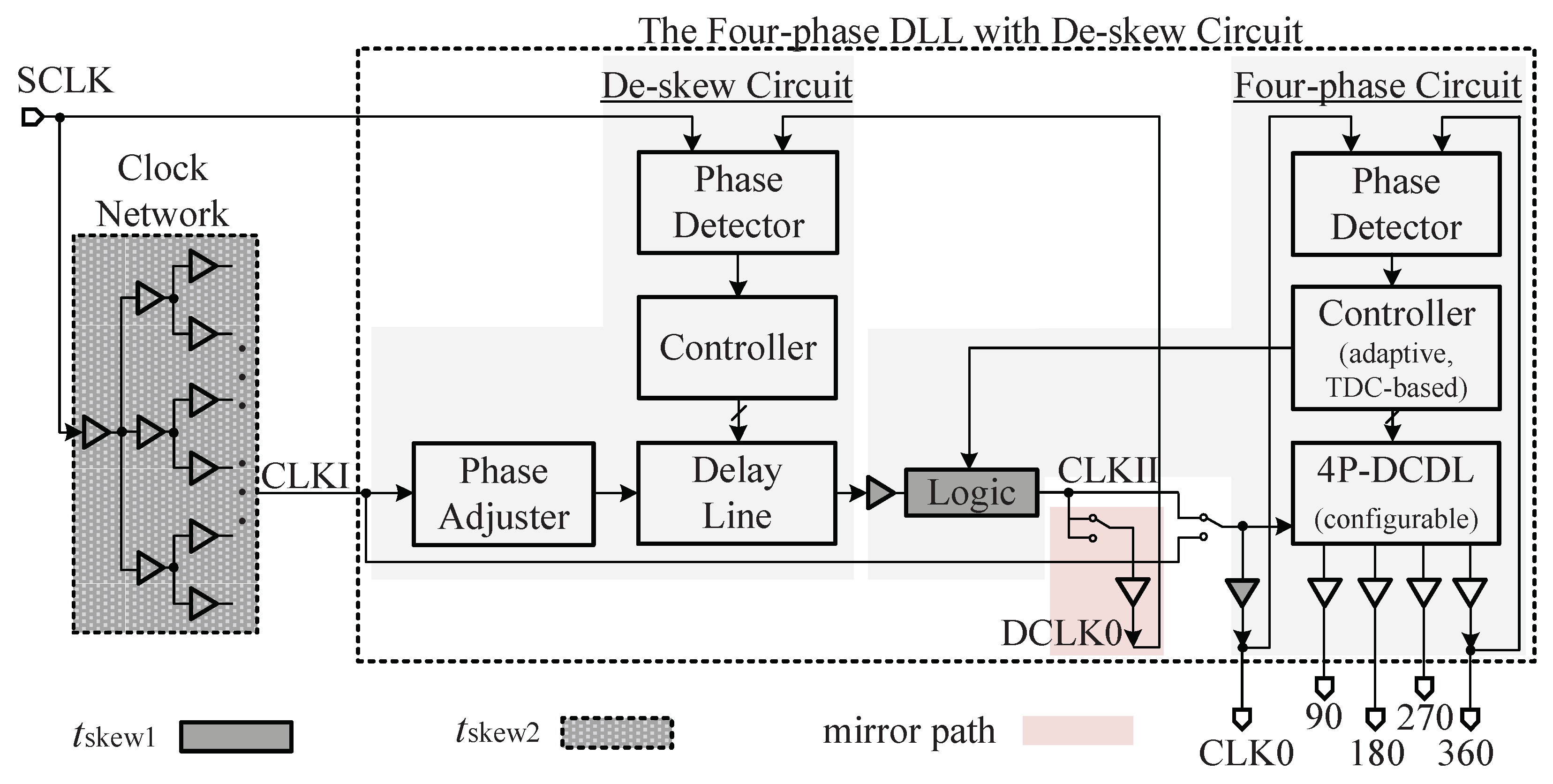
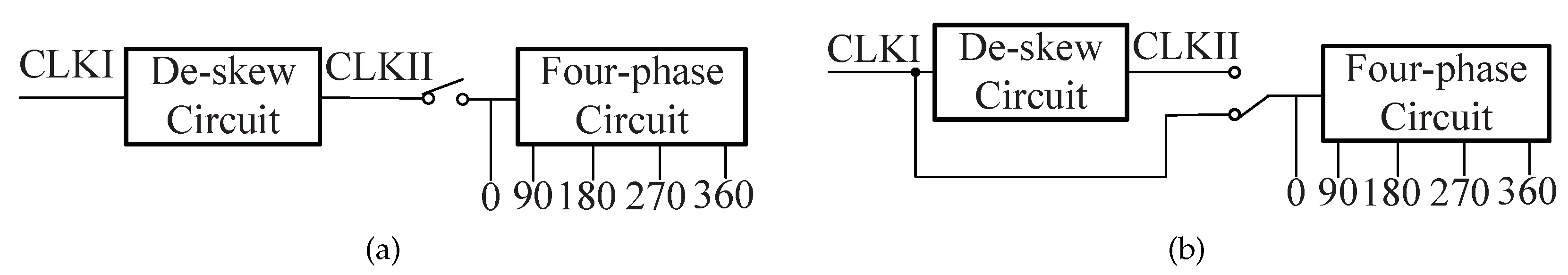
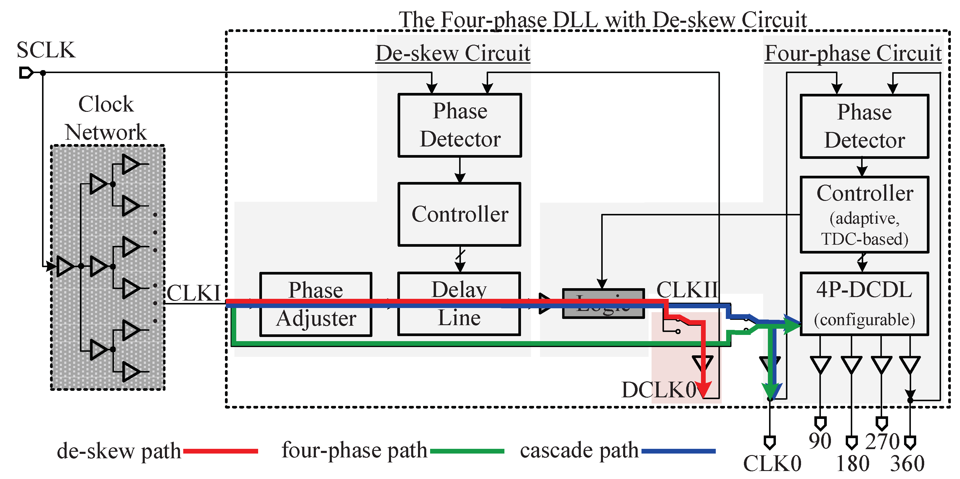
2. The Proposed Four-Phase All-Digital DLL with De-Skew Circuit Architecture

The entire DLL system has two input clocks and five output clocks, as shown in Figure 1. The input clock SCLK is the reference clock of the DLL system and originates from the key node in the clock tree of the NAND Flash interface system. The input clock CLKI is the delayed signal of SCLK, which is used as the synchronized clock of the DLL system to control the locking process. The output clocks CLK0, CLK90, CLK180, CLK270 and CLK360 are multiphase clocks based on SCLK that provide important data strobe signals DQS for data transmission and offer synchronized clocks for critical modules of the NAND Flash interface.
Figure 1 shows the architecture of the proposed four-phase DLL with a de-skew circuit, which consists of a de-skew circuit, a four-phase circuit, a mirror path and a multiplexer (MUX). The DLL system first works in parallel, which enables both de-skew and four-phase circuits, and then changes to cascade after the four-phase circuit is locked. By making the de-skew and four-phase circuits work in parallel in separate loops until the system is locked, the local power supply network of the DLL system remains stable, thus eliminating the variable phase error caused by mode switching. In addition, the parallel operation helps to reduce the total locking period of the overall circuit. The mirror path replicates the MUX and output buffer on the CLK0 path to produce the mirrored output DCLK0, thus allowing the de-skew circuit to compare phase relationships independently. The MUX is used to control the switching of the parallel-cascade configuration. The signal CLKII is an output of the de-skew circuit and also the input clock of the 4P-DCDL in cascaded mode.
The four-phase circuit consists of a phase detector, a TDC-based delay line controller, an adaptive controller and a 4P-DCDL, as shown in Figure 2. To improve the frequency range and phase accuracy, the four-phase circuit adopts the configurable 4P-DCDL and the adaptive controller [16]. The configurable 4P-DCDL is configured for different delay ranges according to the configuration signal SET. The adaptive controller generates the signal SET by quantizing the frequency of the input clock. After being enabled, the four-phase circuit first measures the frequency of the input clock through the adaptive controller and generates signal SET to configure the 4P-DCDL for the appropriate delay range. Then, the TDC-based delay line controller controls the 4P-DCDL to generate delay between the input and output clocks to make the latter lag from the former by exactly one clock cycle. Finally, the 4P-DCDL outputs the four-phase signals by dividing the clock cycle equally.
Since the adaptive controller needs to reuse the 4P-DCDL, the input clock should go through logic units and buffers before entering the 4P-DCDL, which causes a clock skew ( t s k e w 1 ) between SCLK and CLK0. Besides the t s k e w 1 , there is also a clock skew between SCLK and CLK0 caused by the clock network ( t s k e w 2 ), as shown in Figure 1.
The de-skew circuit is embedded in the delay path between SCLK and CLK0 to eliminate the t s k e w 1 and t s k e w 2 , as shown in Figure 1. In parallel mode, the de-skew circuit aligns SCLK and CLK0 by aligning SCLK and DCLK0. To achieve the wide frequency range required by the ONFI protocol, the de-skew circuit in this paper is based on HDSC architecture, which can shorten the delay line without affecting the frequency range, instead of the traditional architecture with a long delay line, which means a large area and high power consumption. The de-skew circuit consists of a phase adjuster, a phase detector, a controller and a delay line. The phase adjuster adjusts the phase of the input clock of the delay line to reduce the delay for skew compensation. The controller changes the number of active units of the delay line to provide the delay for skew compensation, thus aligning the edges of the system clock and the 0 clock output of the four-phase circuit. Finally, the proposed four-phase DLL with de-skew circuit generates the accurate four-phase outputs based on the system clock.
Furthermore, instead of the traditional serial-cascade configuration, the DLL system adopts the proposed parallel-cascade configuration. The former usually works in sequence, and the power current varies in different operating modes, leading to voltage fluctuations in the supply network. Since the unit delay is susceptible to PVT, the voltage fluctuation eventually causes the alignment error of the de-skew circuit to change. In contrast, the latter has almost no power current variation during mode switching and keeps the supply voltage stable during system locking process. Therefore, the parallel-cascade configuration can effectively solve the alignment error variation caused by power supply integrity and ensure the phase-locked accuracy of the DLL system.
The all-digital four-phase DLL with a de-skew circuit begins working with a one-time trigger when the interface system is powered up. After it is locked, all control codes in the DLL are fixed to provide stable four-phase outputs to other circuits in the interface. If the interface system detects a phase error greater than the threshold, the system will send a reset signal to restart the DLL system to obtain new, accurate four-phase outputs.

3. Critical Circuit Description

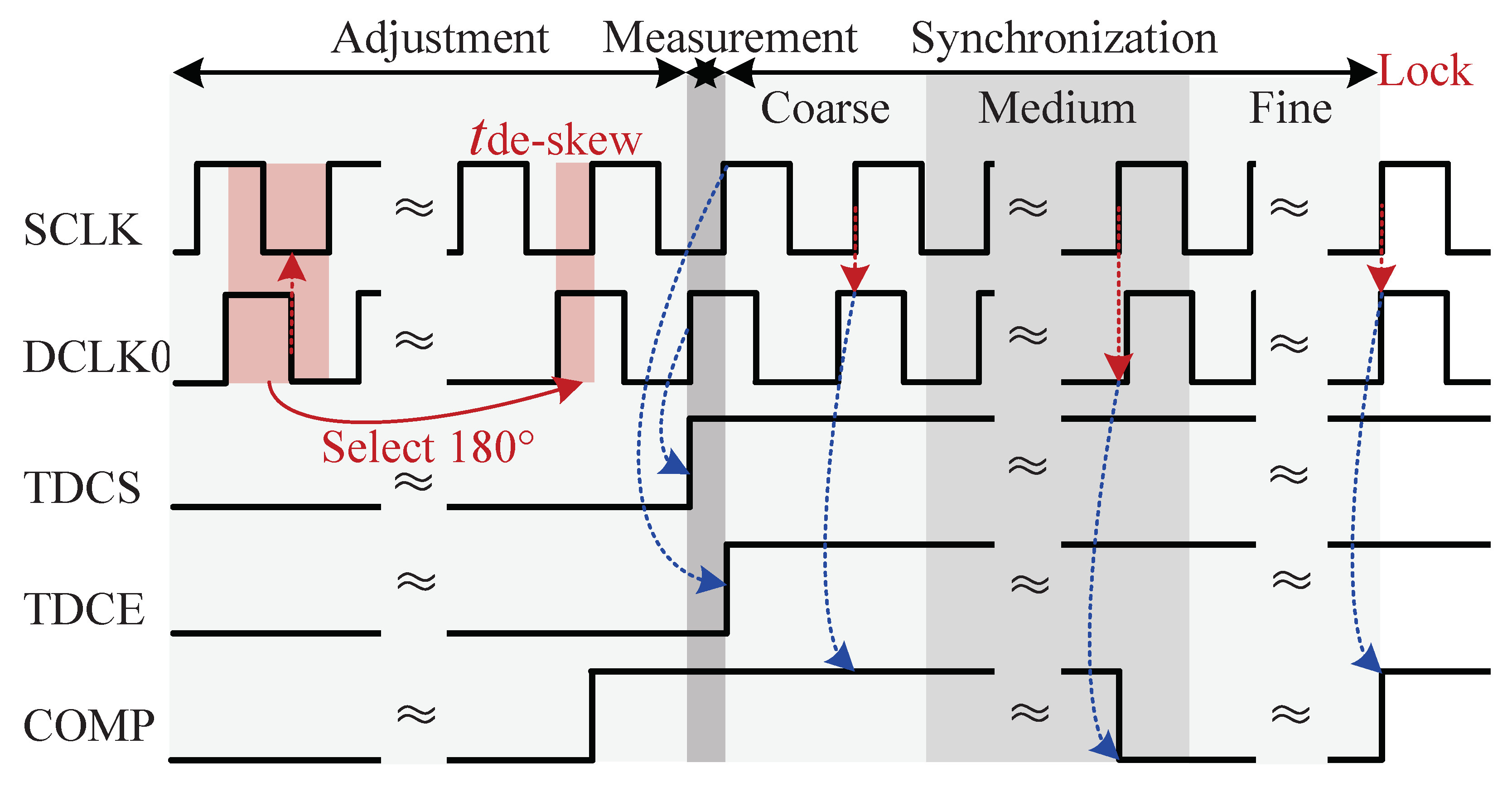
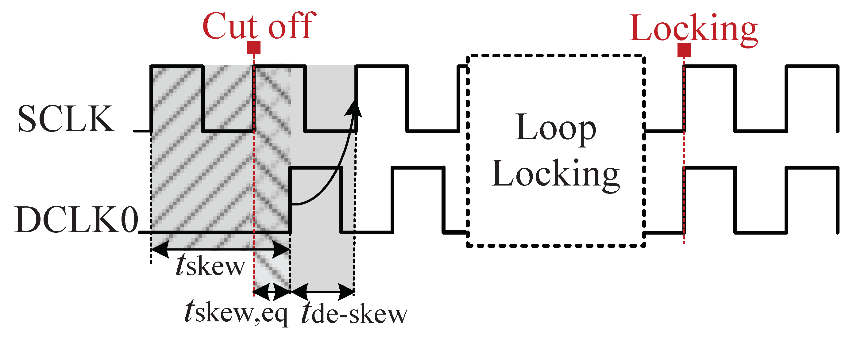
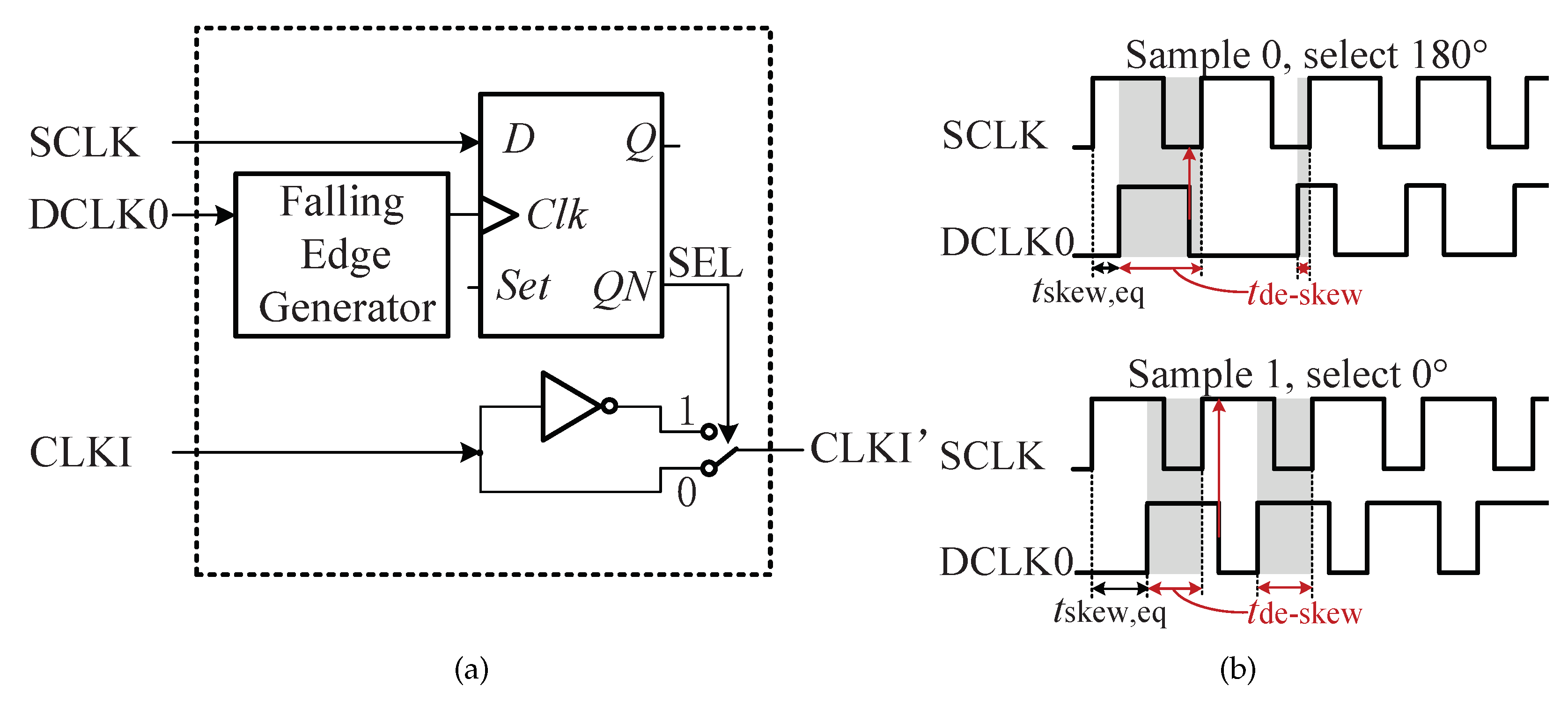
3.1. The Specific Structure of the De-Skew Circuit

Figure 3 shows the specific structure of the de-skew circuit, which consists of a fall-edge-judgment phase adjuster (FPA), a three-stage digitally controlled delay line (3S-DCDL), a phase detector (PD), an edge generator (EG), a timing controller (TC) and a delay line controller. The 3S-DCDL consists of three sub-lines cascaded, namely the coarse delay line (CDL), medium delay line (MDL) and fine delay line (FDL). The delay line controller adopts a coarse–medium–fine structure. The CDL delay is controlled by TDC, and the delays of MDL and FDL are controlled by shift registers.
Figure 4 shows the timing diagram of the de-skew circuit. After being enabled, the de-skew circuit operates the adjustment, measurement and synchronization stages sequentially until the loop is locked.
The purpose of the adjustment stage is to reduce the delay for skew compensation ( t d e - s k e w ) by adjusting the phase of the input clock of 3S-DCDL. In this stage, the 0 of SCLK passes through the initial delay path to generate DCLK0, which is fed back to FPA to compare the phase with SCLK. The comparison result determines whether the input clock phase of 3S-DCDL is the 0 or 180 of SCLK. Figure 4 shows that t d e - s k e w is reduced by half a cycle when 180 of SCLK is adopted.
The goal of the measurement stage is to measure and quantify t d e - s k e w , which is the interval between the edges of SCLK and DCLK0. In this stage, EG captures the edge of DCLK0 and the subsequent edge of SCLK as the start and end edges of TDC, which are noted as TDCS (TDC Start) and TDCE (TDC End), respectively, as shown in Figure 4. Then, TDC quantifies the interval between these two edges into coarse code.
In the synchronization stage, the delay line controller gradually achieves alignment by the coarse–medium–fine tuning mode. First, the coarse code is assigned to the CDL. Because of the measurement error of TDC [15], the DCLK0 is ahead of SCLK after coarse tuning, and the coarse tuning error is limited to a coarse unit delay. After that, the circuit adjusts the delay of MDL by the medium tuning controller, and the medium code increases bit by bit to increase the delay until DCLK0 lags slightly behind SCLK. At this moment, a falling edge appears in the comparison result of the phase detector (COMP), and the medium tuning error is limited to a medium unit delay. Finally, the circuit turns on fine tuning and adopts the fine tuning controller to adjust the delay of FDL. The fine code decreases bit by bit to reduce the delay until DCLK0 is slightly ahead of SCLK, and the COMP has a rising edge. At this point, the de-skew circuit completes loop locking, and the alignment error is limited to a fine unit delay.
At extremely wide operating frequencies, the de-skew circuit may face a situation where the clock skew is longer than one clock cycle, as shown in Figure 5. In this case, since the proposed de-skew circuit is an edge-triggered system, the skew will be cut off by the clock edge, producing an equivalent skew ( t s k e w , e q ) that is always less than the clock period. This can be expressed as Equation (1):
t s k e w , e q = t s k e w t s k e w T × T < T
where is the mathematical rounding down symbol, and T is the clock period. As long as the equivalent skew is eliminated, the de-skew circuit can achieve clock alignment, and the t d e - s k e w is determined by T and t s k e w , e q , which can be given by
t d e - s k e w = T t s k e w , e q < T
In theory, any value of clock skew can be eliminated as long as the delay range of the de-skew circuit covers one clock period. This presents a great solution to solve the unpredictable skew in synchronous interfaces.

3.2. The Proposed Fall-Edge-Judgment Phase Adjuster

The traditional HDSC architecture requires a clock duty cycle of 50%, but the clock may be seriously distorted due to the mismatch between the pull-up and pull-down of clock drivers in the transmission path, making the HDSC lose the advantage in shortening the length of the delay line. The proposed fall-edge-judgment phase adjuster is independent of the clock duty cycle and can be easily applied to the HDSC-based de-skew circuit to widen the frequency range. Figure 6 shows the structure and adjustment strategy of FPA, where signal CLKI is the delayed version of SCLK, the signal CLKI’ is the phase-adjusted version of SCLK, and SEL is the judgment signal in the FPA. In the adjustment stage of the de-skew circuit, FPA selects 0 or 180 of CLKI for CLKI’ according to the relationship between the falling edge of DCLK0 and the high/low levels of SCLK.
As shown in Figure 6b, when the falling edge of DCLK0 samples the low level of SCLK, the FPA outputs 180 of CLKI. The new DCLK0 rising edge will appear at the position of the previous falling edge; then, t d e - s k e w rapidly changes from greater than the low-level pulse width of clock ( t l o w ) to less than t l o w . This can be expressed as Equation (3):
t d e - s k e w = T ( t s k e w , e q + t h i g h ) t l o w
where t h i g h is the high-level pulse width of the clock. Conversely, when the falling edge of DCLK0 falls into the high level of SCLK, FPA outputs the 0 of CLKI, and t d e - s k e w is less than t h i g h . It can be expressed as Equation (4):
t d e - s k e w = T t s k e w , e q t h i g h
Thus, t d e - s k e w is less than max ( t h i g h , t l o w ) after phase adjustment. At a defined clock frequency with a duty cycle distortion level of x, max ( t h i g h , t l o w ) is ( 50 % + x % ) of the clock period, so the delay range of de-skew circuit only needs to cover ( 50 % + x % ) × T to ensure locking. If the sampling is based on the rising edge, DCLK0 samples high level and FPA selects 180 of SCLK in both cases of Figure 6b. Obviously, in the second case, if FPA selects 180 , t d e - s k e w will be greater than t h i g h , and the delay line range needs to cover the entire cycle to ensure locking, which indicates that HDSC has lost the advantage in shortening the delay line. The falling edge contains information of the duty cycle distortion, which is the basis of the FPA judgment strategy.
According to the basic principle of the de-skew circuit, the maximum delay of the delay line ( T D C D L , m a x ) determines the minimum operation frequency of circuit ( f m i n ). Thus, without the phase adjustment stage, f m i n can be expressed as Equation (5):
f m i n = 1 T D C D L , m a x + t i n t
where t i n t is the intrinsic delay of other logic units and buffers in the delay path. With the same length of the delay line, when the phase adjustment stage is added, f m i n is given by
f m i n = 50 % + x % T D C D L , m a x + t i n t
In summary, with a certain delay line length, the HDSC-based de-skew circuit with a duty-cycle-independent FPA can widen the operating frequency range.

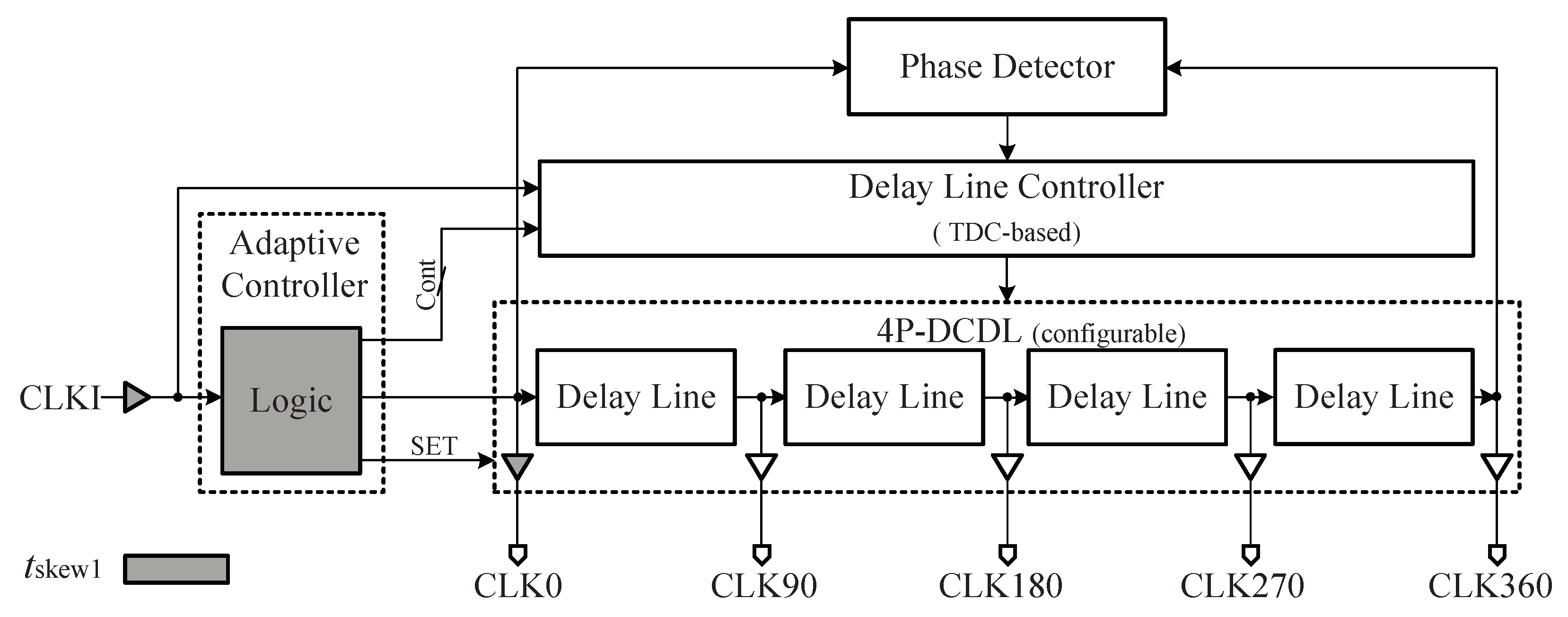
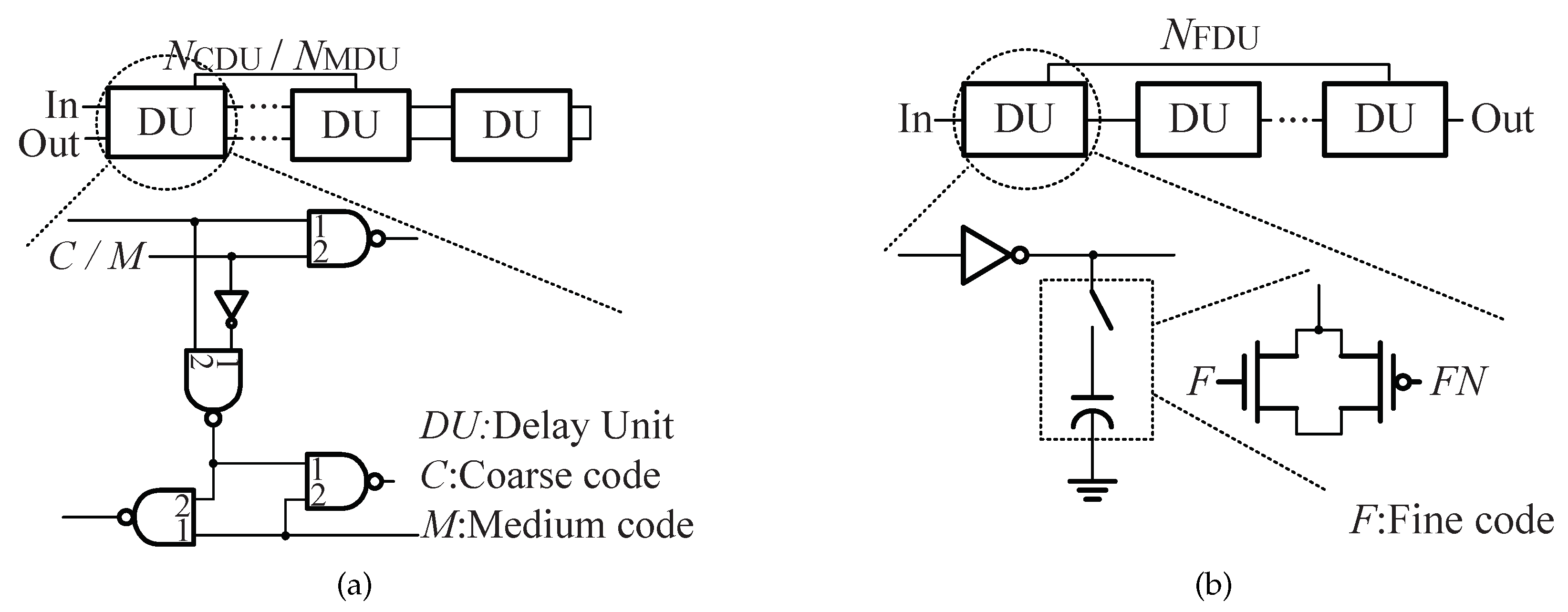
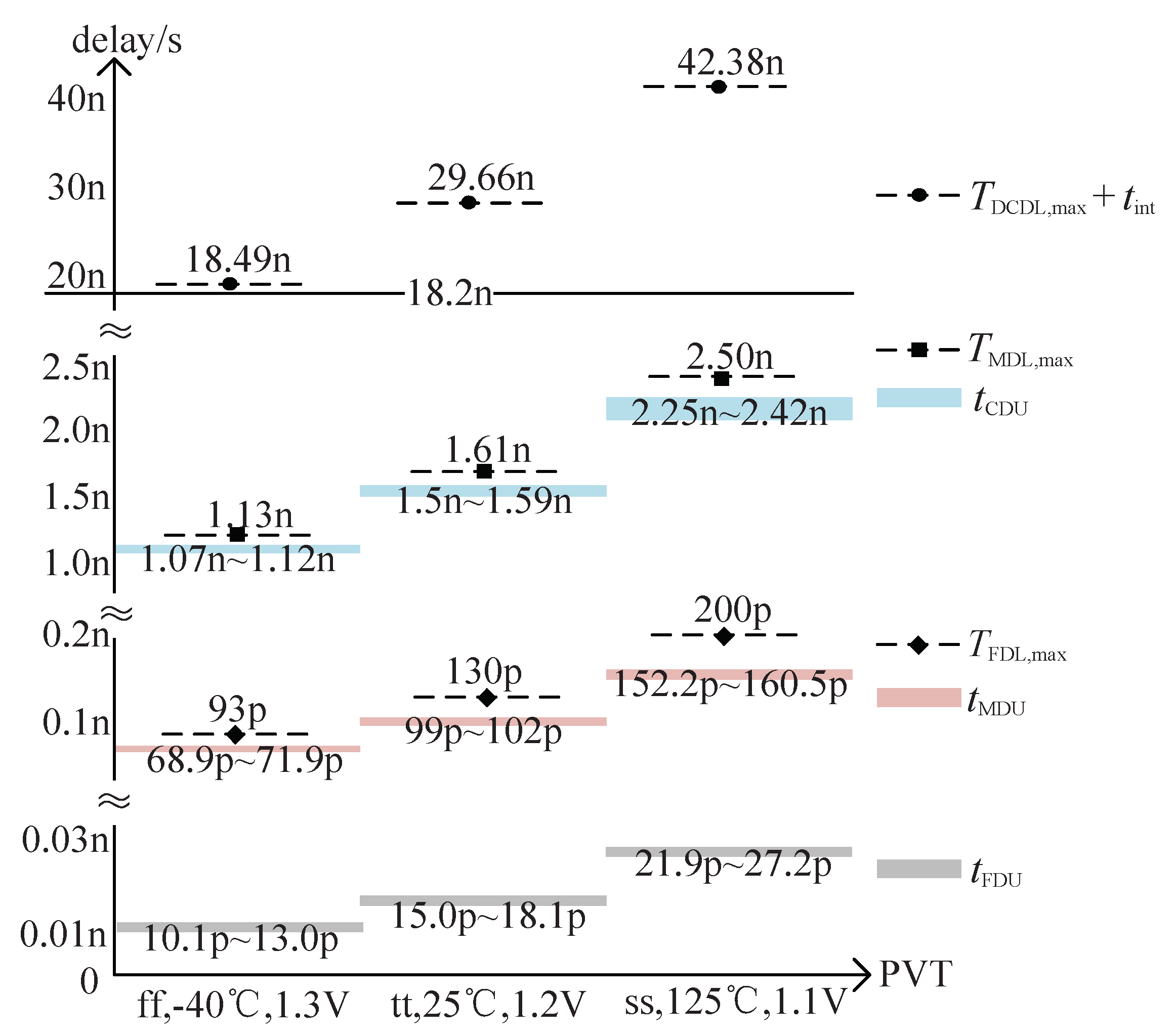
3.3. The Three-Stage Digitally Controlled Delay Line

To achieve the de-skew circuit with a wide frequency range and high phase accuracy, the delay line is designed as a three-level structure, consisting of CDL, MDL and FDL cascaded. Figure 7 shows the structure and unit of sub-lines. The delay units of CDL and MDL are based on NAND gates to save power consumption [23]. To achieve a fine delay, the delay unit of FDL is composed of an inverter and a capacitor. The capacitor is implemented by a transmission gate (TG), which generates a small propagation delay difference by the difference in load effect between its on and off states [24], thus achieving a fine delay. The cascaded inverter in the fine delay unit is used to restore the driving capability of the delay path.
Through the optimized design of the sub-lines to cover the frequency range required by the protocol, the adjustment range of MDL ( T M D L , m a x ) should cover the unit delay of CDL ( t C D U ) and the adjustment range of the FDL ( T F D L , m a x ) should cover the unit delay of MDL ( t M D U ), even in the case of PVT variations. The above relationships can be expressed as Equations (7) and (8):
t C D U T M D L , m a x = N M D U × t M D U
t M D U T F D L , m a x = N F D U × t F D U
where N M D U and N F D U are the unit numbers of MDL and FDL, respectively, and t F D U is the unit delay of FDL.
The maximum delay of 3S-DCDL ( T D C D L , m a x ) determines the minimum operating frequency of the de-skew circuit, and the finest unit delay determines the phase accuracy of the de-skew circuit ( T s t e p ). Thus, T D C D L , m a x and T s t e p are given by Equations (9) and (10):
T D C D L , m a x = T D C D L , i n t + N C D U × t C D U
T s t e p = t F D U
where N C D U is the unit number of CDL, and T D C D L , i n t is the intrinsic delay of 3S-DCDL. The maximum operating frequency ( f m a x ) of the HDSC-based de-skew circuit is limited by the CMOS process, and the minimum operating frequency ( f m i n ) is shown in Equation (6). Therefore, on the premise of satisfying Equations (7) and (8), the proposed de-skew circuit can achieve a wider frequency range and higher phase accuracy by optimizing the parameters N C D U , t C D U and t F D U .

4. The Proposed Parallel-Cascade Configuration

This paper proposes a parallel-cascade configuration to solve the variable phase alignment problem caused by voltage fluctuations during mode switching in the serial-cascade configuration. The configurations of the de-skew circuit and four-phase circuit are shown in Figure 8.
Figure 8a shows the traditional serial-cascade configuration of the DLL system. In this configuration, the system first enables the de-skew circuit for the phase-alignment mode to generate a stable clock output CLKII and then enables the four-phase circuit for the four-phase outputs generation mode. However, a potential problem has been discovered during post-layout simulation: when switching between different modes, this configuration causes a variable phase error related to the clock frequency due to power integrity issues. The root cause of this problem is that during the four-phase output generation mode, a large number of delay units and control units in the four-phase DLL are enabled, and the total system current increases significantly. The obvious increase of the operating current causes a larger IR drop on the supply network, which means that the supply voltage of the delay unit is reduced. Since the gate delay of a delay unit is closely related to the supply voltage, the delay of units in the delay path all change, including the units that generate skew and compensate for skew, thus causing an additional alignment error between SCLK and CLK0. At 25 °C, 1.2 V, tt, f c l o c k = 800 MHz, Figure 9 shows that the average power current of the system is 4.09 mA during the de-skew mode, which increases to 9.58 mA during the four-phase outputs generation mode after switching, which leads to an increase of 40.12 ps in the alignment error between SCLK and CLK0. This phase error varies with the total number of units activated in the four-phase output generation mode at different frequencies, so it cannot be eliminated by only improving the matching of circuit and layout.
To solve this problem, a parallel-cascade configuration is proposed in this paper, as shown in Figure 8b. The DLL system first operates in parallel mode with both de-skew and four-phase circuits enabled and then changes to cascade mode after the four-phase circuit is locked. By working in parallel, the delay and control units required for locking at this frequency are enabled, so the total current of the power supply network remains stable during the loop locking process, thus solving the variable alignment error caused by serial-cascade configurations. As shown in Figure 10, the average power current keeps stable at around 10 mA during the locking process, and the alignment error after locking keeps at 8.12 ps. In addition, another advantage of the parallel-cascade configuration is that it reduces the total locking cycles compared to the serial-cascade configuration by working in parallel.
In order to support the proposed configuration, as shown in Figure 11, a mirror path is added to the input of 4P-DCDL to make the de-skew path and the four-phase path independent of each other, providing a stable input clock to two loops, respectively, which enhances the robustness of the system; a MUX is added to control the mode switching, and the error caused by switching is minimized by matching the path delay of CLK0 and its mirror output DCLK0. In addition, with the feature that the locking cycles of de-skew circuit are larger than that of four-phase circuit, the loop of the de-skew circuit can track the skew during the remaining locking cycles. After the four-phase circuit is locked, its control codes are fixed to maintain the phase relationships between the four-phase clocks. The input clock of the four-phase circuit is then switched from CLKI to CLKII, which is not yet fully de-skewed. Once the de-skew circuit finishes its locking process, CLK0 will be aligned with SCLK. The proposed parallel-cascade configuration can maintain the stability of the local power supply network of the individual DLL system; however, due to the sensitivity of clock circuit to the voltage network, it still needs to be optimized with the multi power supply network to avoid the impact on clock network performance from the activity of high power consumption modules outside the DLL system.

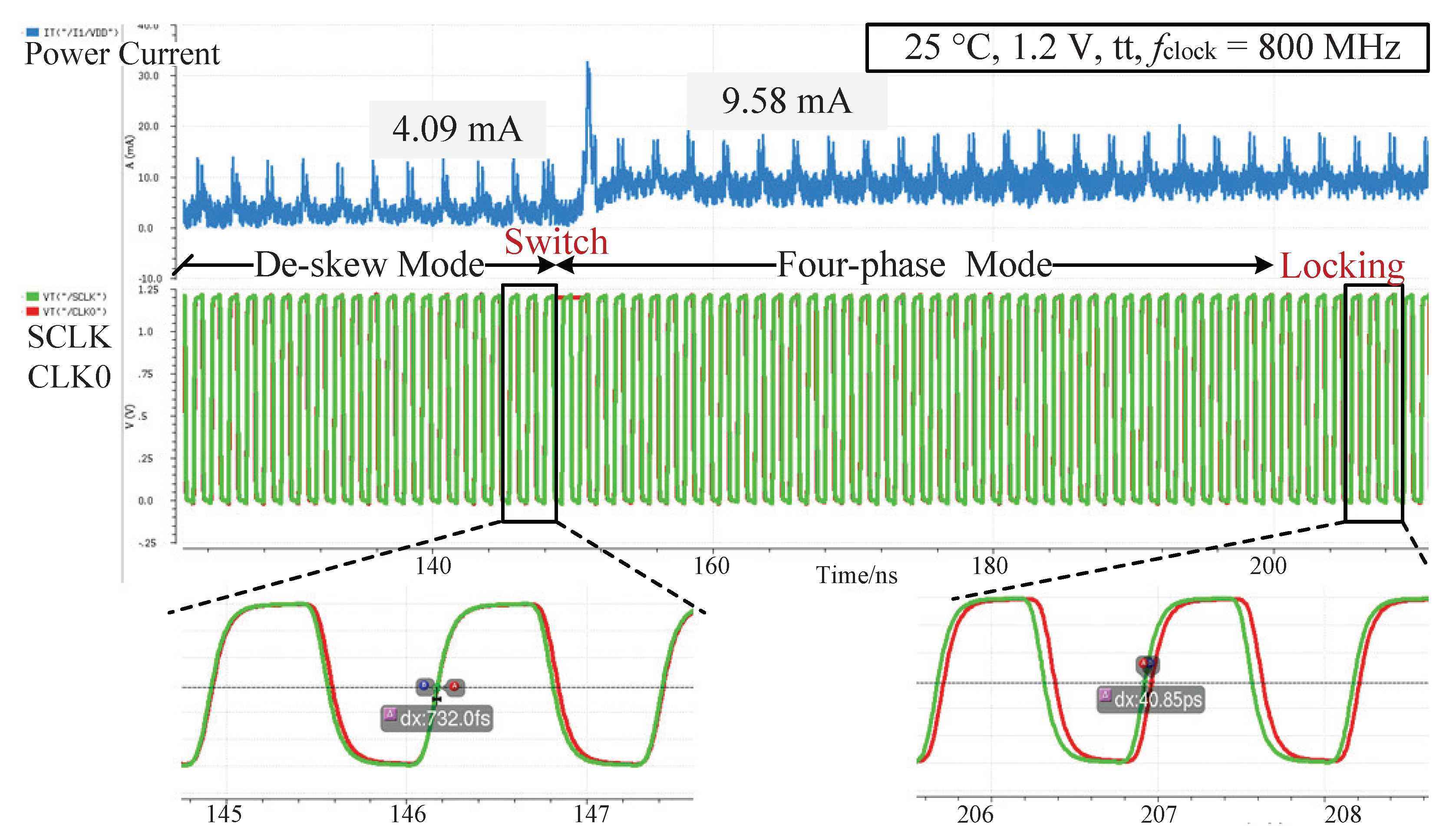
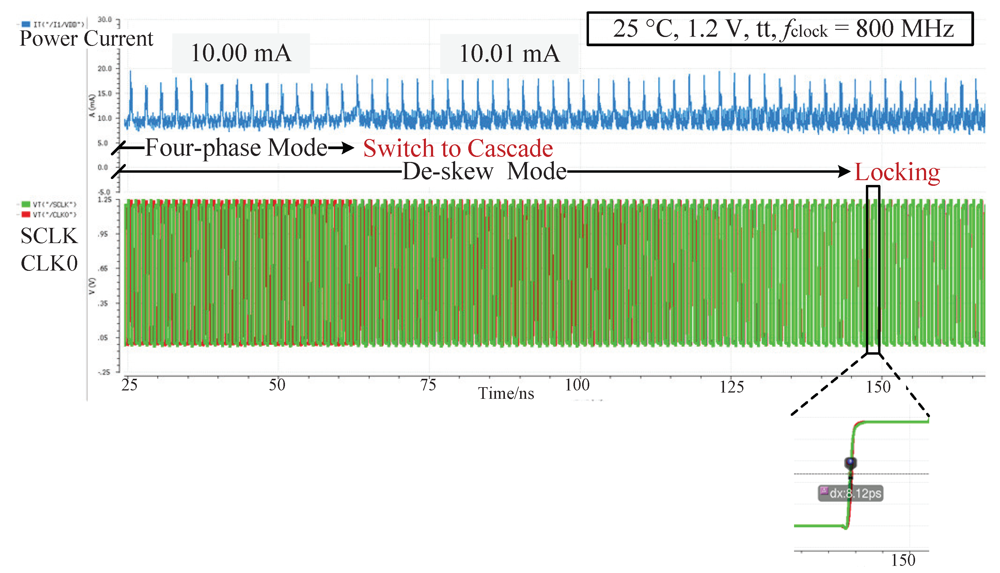
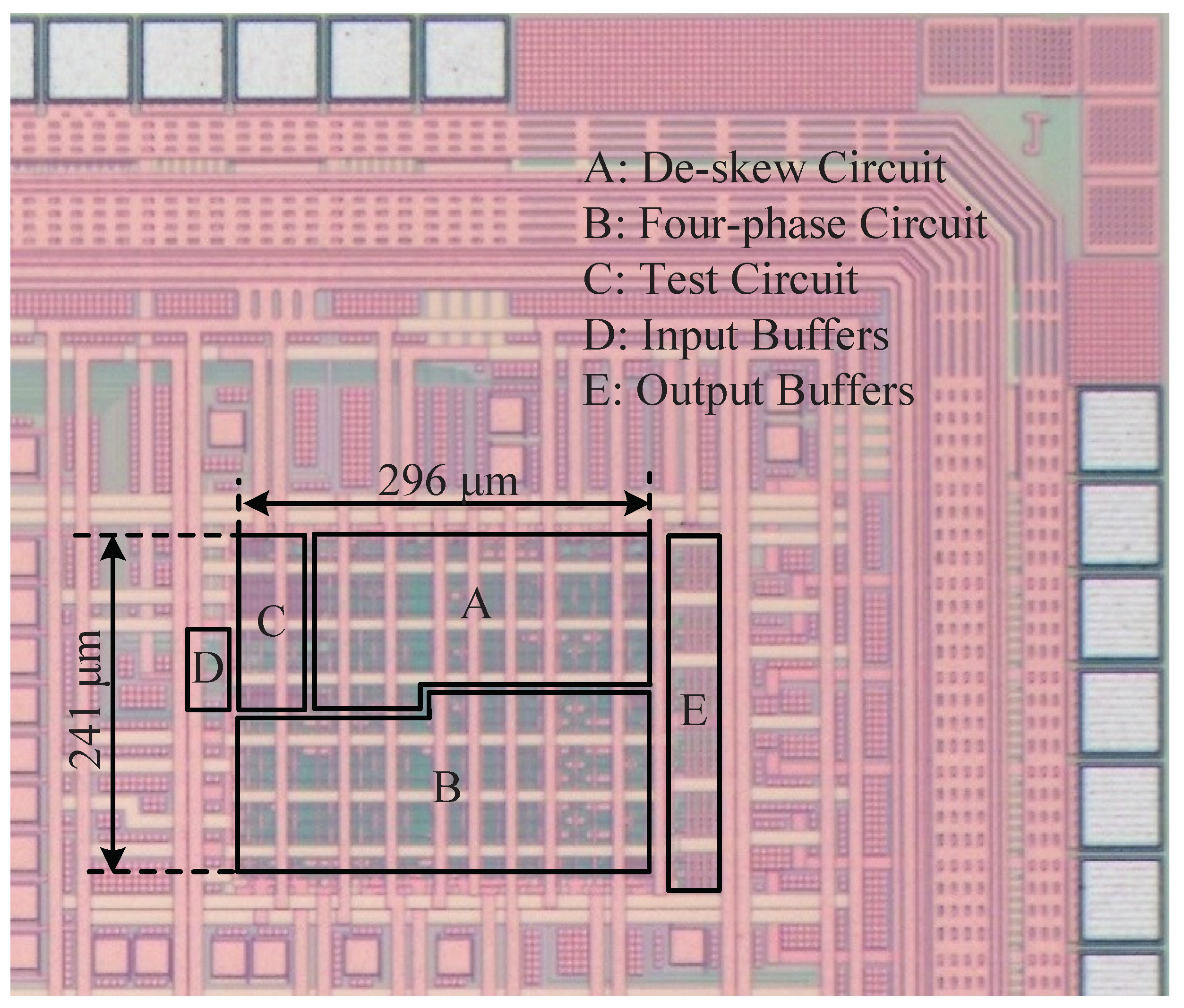
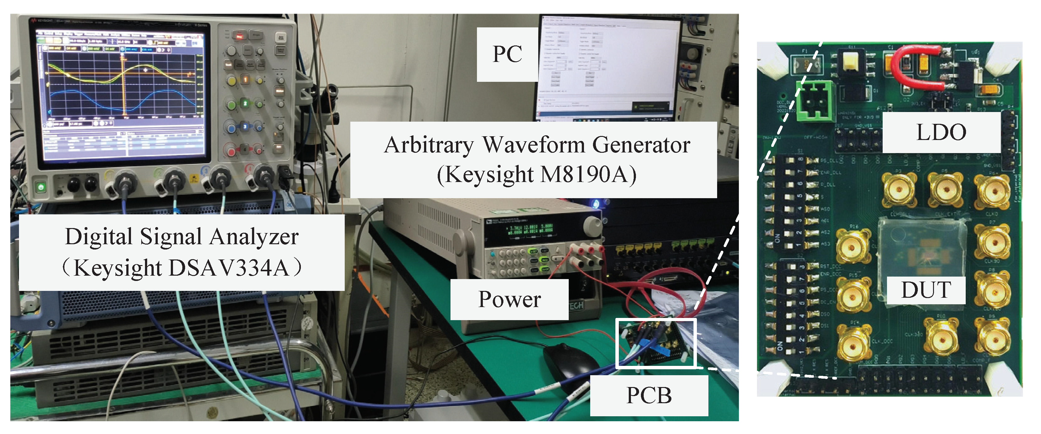
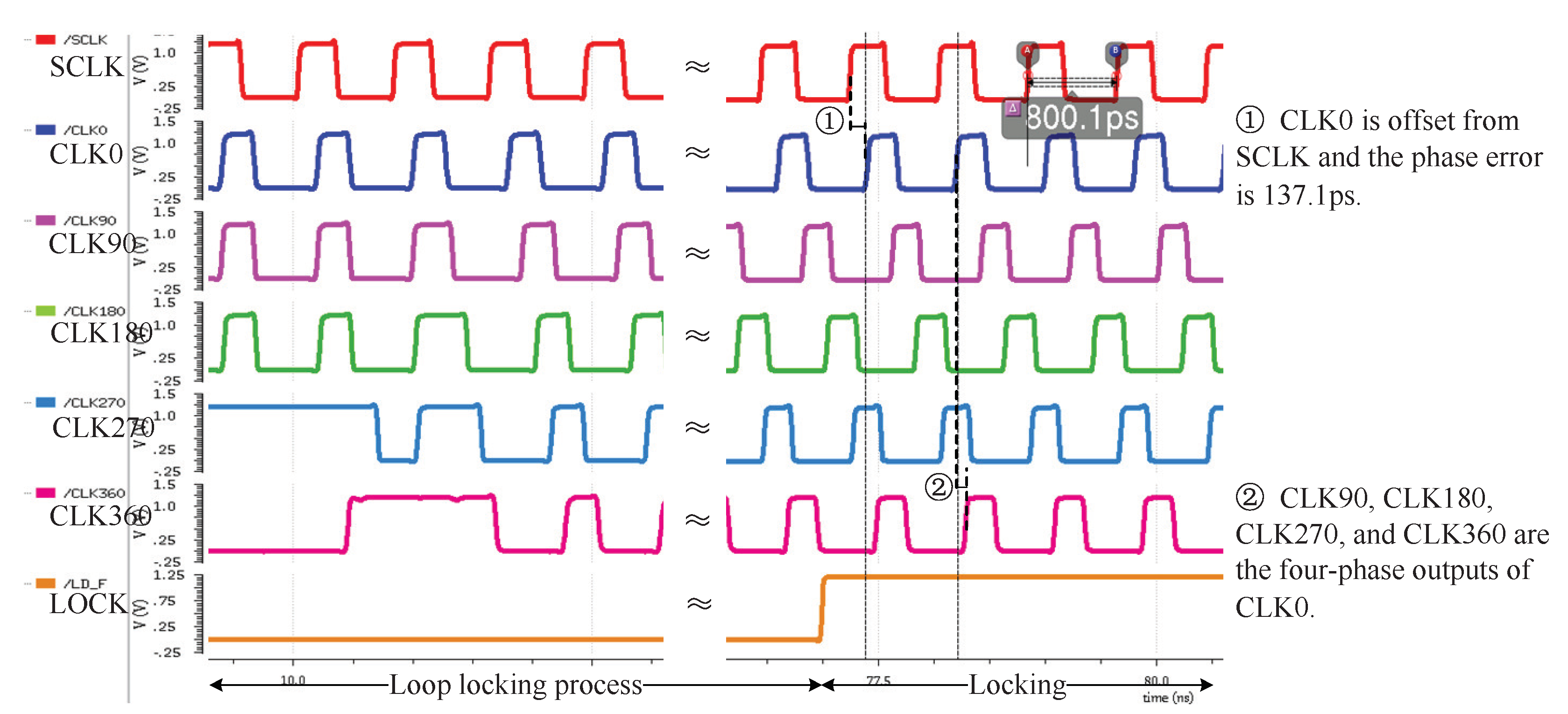
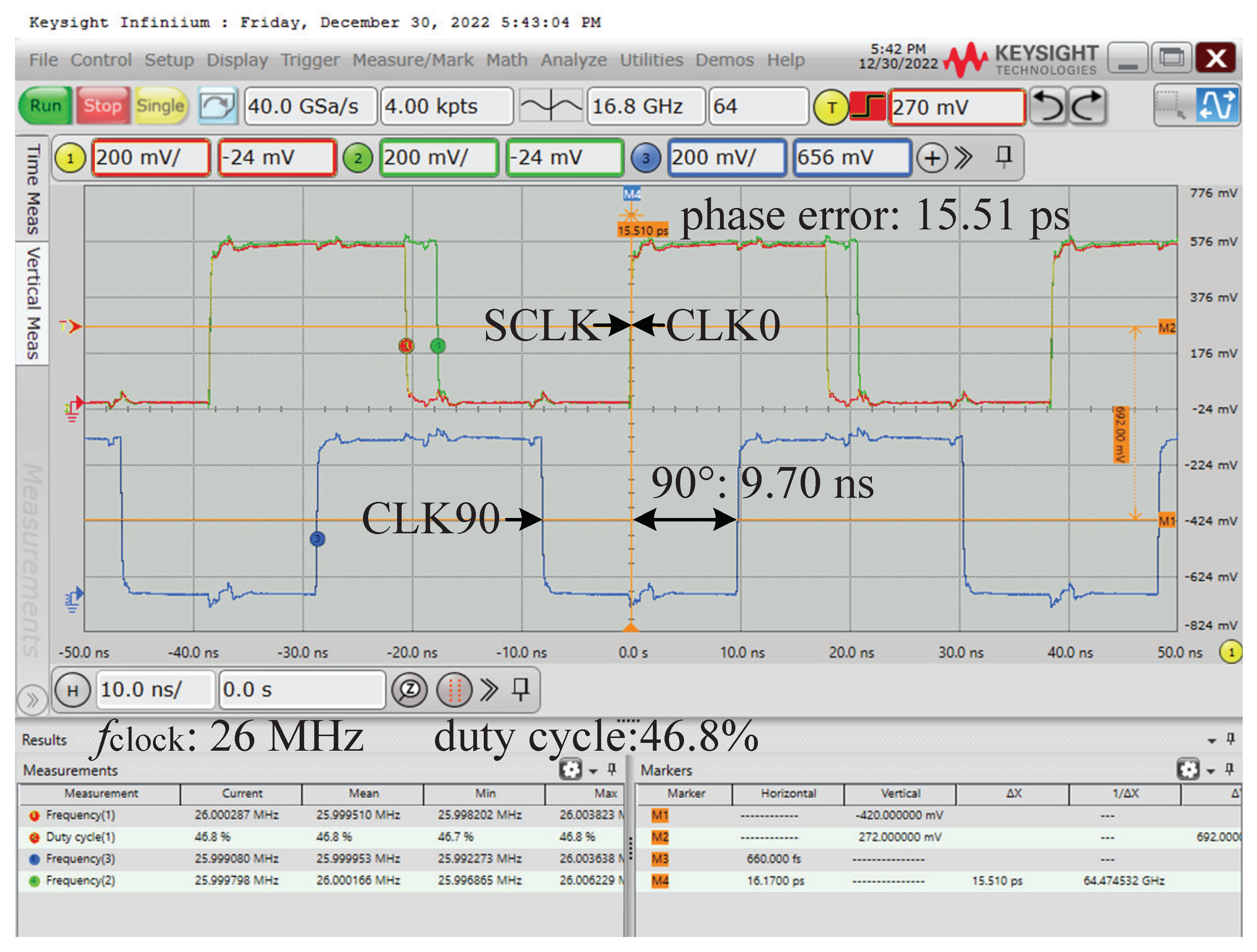
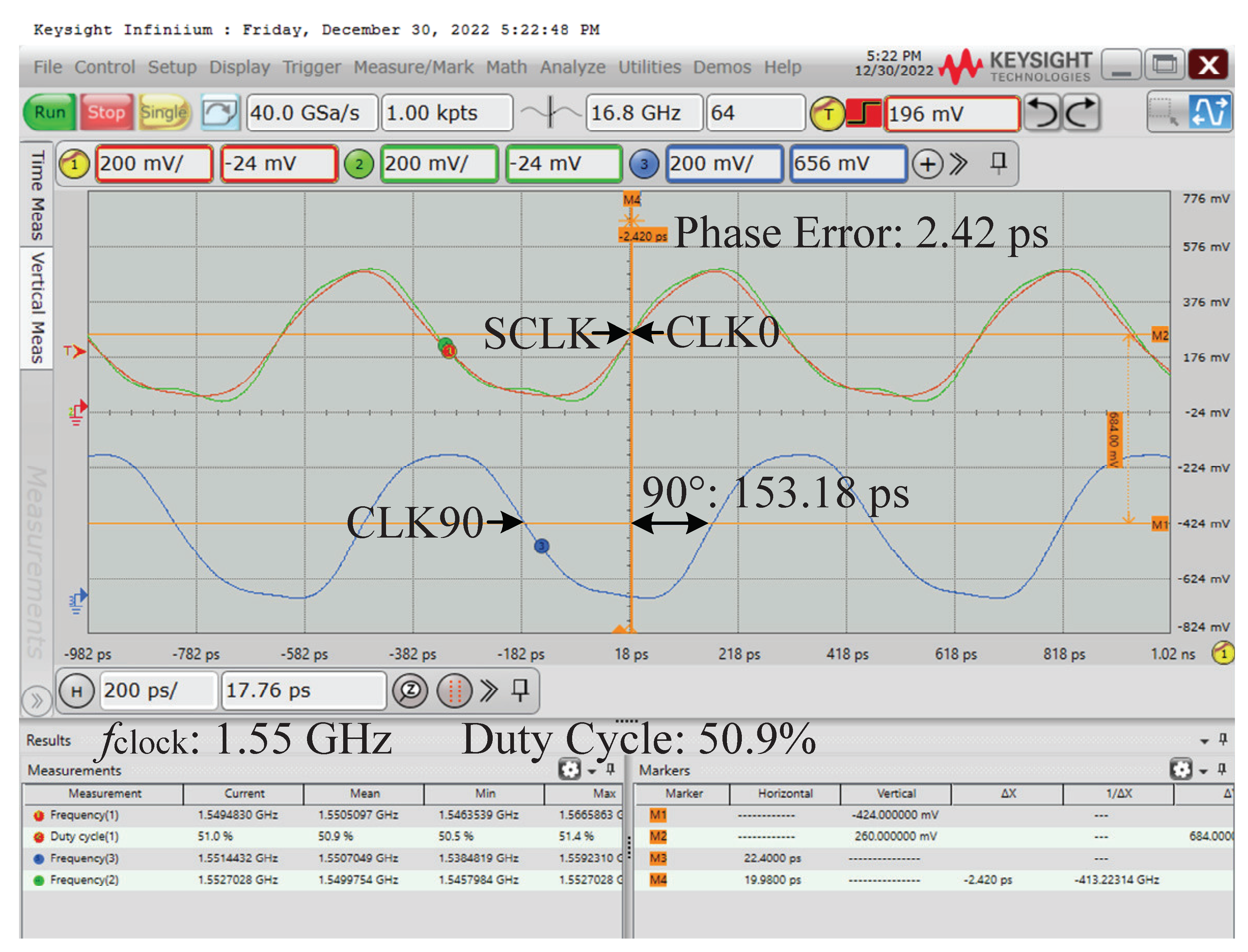
5. The Experimental Results

The proposed four-phase all-digital DLL with a de-skew circuit is fabricated in a 0.13 μ m CMOS process. Considering the frequency range and phase accuracy requirements of the ONFI protocol, this paper chooses N C D U = N M D U = 16 and N F D U = 8 . The micrograph of the test chip is shown in Figure 12 with a core area of 0.072 mm 2 . The testbench and printed circuit board (PCB) are shown in Figure 13. The arbitrary waveform generator (M8190A, Keysight) provided an input clock with a frequency range of 26 MHz to 1.55 GHz for the test chip, and the power supply provided a 3.3 V DC voltage to the PCB, which was converted by the low dropout regulator (LDO) to 1.2 V for the chip. The multi-channel high-frequency signals were captured with the digital signal analyzer (DSAV334A, Keysight).
Figure 14 shows the delay range and unit delay of sub-lines in the de-skew circuit under different PVT conditions, from which three inferences can be drawn. First, the T M D L , m a x can cover the t C D U and the T F D L , m a x can cover the t M D U , even in the case of PVT variations. These relationships are consistent with Equations (7) and (8), which indicates that the de-skew circuit can cover the required frequency range. Second, according to Equation (6), for the case that the duty cycle distortion factor is 10, the delay path length T D C D L , m a x + t i n t cannot be lower than 18.2 ns to meet the ONFI 5.0 requirements for f m i n = 33 MHz. The data show that T D C D L , m a x + t i n t is greater than 18.2 ns under different PVT conditions, so this design can cover the f m i n of 33 MHz. Third, considering the N F D U = 8 , the phase accuracy of the de-skew circuit is T s t e p = t F D U = T F D L , m a x / N F D U = 130 ps/8 ≈ 17 ps.
Figure 15 and Figure 16 show the comparative results of the four-phase DLL without de-skew circuit and four-phase DLL with de-skew circuit, respectively. It can be seen from Figure 15 that CLK90, CLK80, CLK270 and CLK360 are the exact four-phase outputs based on CLK0 instead of SCLK. This is because the unpredictable clock skew exists between CLK0 and SCLK, causing the four-phase outputs to be offset from SCLK. In Figure 16, since the embedded de-skew circuit eliminates clock skew, CLK90, CLK180, CLK270 and CLK360 are the exact four-phase outputs based on SCLK. In addition, with f c l o c k = 1.25 GHz and a 40% duty cycle as shown in Figure 16, the proposed FPA can correctly adjust the clock phase in the case of duty cycle distortion.
Figure 17 and Figure 18 show the chip testing results, where the proposed circuit has an alignment error of 15.51 ps at f c l o c k = 26 MHz with 46.8% duty cycle and 2.42 ps at f c l o c k = 1.55 GHz with 50.9% duty cycle. They also show that the operating frequency ranges from 26 MHz to 1.55 GHz and the typical alignment error is about 17 ps, which fully meets the requirements of the ONFI 5.0 protocol for NAND Flash high-speed interfaces. Moreover, due to the advantages of the high portability and stability of the ADDLL, the circuit easily achieves higher operating frequencies by porting the advanced process to meet the updates of the ONFI protocol.
Table 1 compares the performance of DLLs. It can be seen that the proposed DLL supports both four-phase clock outputs and clock skew elimination and achieves a wide frequency range while maintaining high accuracy and low power consumption, which is suitable for NAND Flash high-speed interfaces.

6. Conclusions

In this paper, a wide-range four-phase all-digital DLL with a de-skew circuit is presented. An HDSC-based de-skew circuit is proposed, which adopts the fall-edge-judgment phase adjuster and the three-stage digitally controlled delay line to accurately align the system clock and the 0 clock output over a wide frequency range. The proposed parallel-cascade configuration maintains the stability of the voltage network during the whole locking process to solve the variable phase alignment problem caused by the mode switching of the serial-cascade configuration. Fabricated in a 0.13 μ m 1.2 V CMOS process, the test chip achieves an operating frequency range of 26 MHz to 1.55 GHz, a typical alignment error of about 17 ps and a core area of 0.072 mm 2 , which fully meets the requirements of ONFI 5.0.

Author Contributions

Conceptualization, J.K. and F.L.; methodology, J.K., F.L., Y.H. and Y.W.; software, J.K.; validation, J.K.; formal analysis, J.K.; investigation, J.K.; data curation, J.K.; writing—original draft preparation, J.K.; writing—review and editing, J.K., F.L., Y.H. and Y.W.; visualization, J.K.; supervision, F.L.; project administration, F.L. All authors have read and agreed to the published version of the manuscript.

Funding

This work was funded by the National Key Research and Development Program of China under grant number 2022YFF1202302, and the Beijing Science and Technology Plan under grant number Z201100004320006.

Data Availability Statement

The data presented in this study are available in article.

Acknowledgments

The authors would like to acknowledge the professors and peers at the Institute of the Microelectronics of the Chinese Academy of Sciences and the University of Chinese Academy of Sciences for knowledge sharing and equipment supporting.

Conflicts of Interest

The authors declare no conflict of interest.

Abbreviations

The following abbreviations are used in this manuscript:
DLLDelay-locked loop
FPAFall-edge-judgment phase adjuster
3S-DCDLThree-stage digitally controlled delay line
ADDLLAll digital delay-locked loop
DDRDouble data rate
ONFIOpen NAND Flash Interface Specification
NV-DDRNon-volatile double data rate
DQSData strobe signal
DQData signal
PVTProcess, voltage and temperature
BERBit error rate
4P-DCDLFour-phase digitally controlled delay line
PDPhase detector
EGEdge generator
TDCTime-to-digital converter
CDLCoarse delay line
MDLMedium delay line
FDLFine delay line
TGTransmission gate
PCBPrinted circuit board
LDOLow dropout regulator

References

  1. Liang, C.K.; Yang, R.J.; Liu, S.I. An All-Digital Fast-Locking Programmable DLL-Based Clock Generator. IEEE Trans. Circuits Syst. I Regul. Pap. 2008, 55, 361–369. [Google Scholar] [CrossRef]
  2. Tsai, C.W.; Chiu, Y.T.; Tu, Y.H.; Cheng, K.H. A wide-range all-digital delay-locked loop for double data rate synchronous dynamic random access memory application. In Proceedings of the 2018 IEEE International Symposium on Circuits and Systems (ISCAS), Florence, Italy, 27–30 May 2018; pp. 1–4. [Google Scholar]
  3. Yao, C.Y.; Ho, Y.H.; Chiu, Y.Y.; Yang, R.J. Designing a SAR-based all-digital delay-locked loop with constant acquisition cycles using a resettable delay line. IEEE Trans. Very Large Scale Integr. (VLSI) Syst. 2014, 23, 567–574. [Google Scholar] [CrossRef]
  4. Chen, H.; Ma, S.; Wang, L.; Zhang, H.; Pan, K.; Cheng, Y. A low-power, area-efficient all-digital delay-locked loop for DDR3 SDRAM controller. Sci. China Inf. Sci. 2014, 12, 1–8. [Google Scholar] [CrossRef] [Green Version]
  5. Keerthi Kumar, M.; Pasupathy, K.R.; Bindu, B. Design of FinFET based All-Digital DLL for multiphase clock generation. In Proceedings of the 2015 Annual IEEE India Conference (INDICON), New Delhi, India, 17–20 December 2015; pp. 1–4. [Google Scholar] [CrossRef]
  6. Lo, Y.L.; Chou, P.Y.; Cheng, H.H.; Tsai, S.F.; Yang, W.B. An all-digital DLL with dual-loop control for multiphase clock generator. In Proceedings of the 2011 International Symposium on Integrated Circuits, Singapore, 12–14 December 2011; pp. 388–391. [Google Scholar]
  7. El-Shafie, A.H.A.; Habib, S.E.D. An all-digital DLL using novel harmonic-free and multi-bit SAR techniques. Microelectron. J. 2012, 43, 393–400. [Google Scholar] [CrossRef]
  8. Chae, K.; Choi, J.; Yi, S.; Lee, W.; Joo, S.; Kim, H.; Yi, H.; Nam, Y.; Choi, J.; Park, S.; et al. A 690mV 4.4 Gbps/pin all-digital LPDDR4 PHY in 10nm FinFET technology. In Proceedings of the ESSCIRC Conference 2016: 42nd European Solid-State Circuits Conference, Lausanne, Switzerland, 12–15 September; pp. 461–464.
  9. Kim, Y.S.; Lee, S.K.; Park, H.J.; Sim, J.Y. A 110 MHz to 1.4 GHz locking 40-phase all-digital DLL. IEEE J. Solid-State Circuits 2011, 46, 435–444. [Google Scholar] [CrossRef]
  10. Tu, Y.H.; Liu, J.C.; Cheng, K.H.; Hsu, C.H. A 0.5-V all-digital clock-deskew buffer with I/Q phase outputs. Analog Integr. Circuits Signal Process. 2017, 93, 157–167. [Google Scholar] [CrossRef]
  11. Bae, J.H.; Seo, J.H.; Yeo, H.S.; Kim, J.W.; Sim, J.Y.; Park, H.J. An all-digital 90-degree phase-shift DLL with loop-embedded DCC for 1.6 Gbps DDR interface. In Proceedings of the 2007 IEEE Custom Integrated Circuits Conference, San Jose, CA, USA, 16–19 September 2007; pp. 373–376. [Google Scholar]
  12. Kumar, A.; Ardeshana, J.; Jagtap, S. Design & verification of ONFI complient high performance NAND flash controller. In Proceedings of the 2016 IEEE International Conference on Recent Trends in Electronics, Information & Communication Technology (RTEICT), Bangalore, India, 20–21 May 2016; pp. 942–945. [Google Scholar] [CrossRef]
  13. Yamini, N.; Sasipriya, P.; Bhaaskaran, V.K. Clock distribution network design for single phase energy recovery circuits. In Proceedings of the 2017 International Conference on Nextgen Electronic Technologies: Silicon to Software (ICNETS2), Chennai, India, 23–25 March 2017; pp. 413–418. [Google Scholar]
  14. Chong, A.B. Hybrid Multisource Clock Tree Synthesis. In Proceedings of the 2021 28th IEEE International Conference on Electronics, Circuits, and Systems (ICECS), Dubai, United Arab Emirates, 28 November–1 December 2021; pp. 1–6. [Google Scholar]
  15. Park, D.; Kim, J. A 7-GHz Fast-Lock 2-Step TDC-based All-Digital DLL for Post-DDR4 SDRAMs. In Proceedings of the 2018 IEEE International Symposium on Circuits and Systems (ISCAS), Florence, Italy, 27–30 May 2018; pp. 1–4. [Google Scholar] [CrossRef]
  16. Yang, X.; Liu, F.; Huo, Z. A wide-range and high-accuracy four-phase delay-locked-loop with adaptive-bandwidth scheme. J. Xidian Univ. 2022, 49, 194–201. [Google Scholar] [CrossRef]
  17. Herath, V.R.; Noé, R. A simple mean clock skew estimation algorithm for clock distribution networks in presence of random process variations and nonuniform substrate temperature. In Proceedings of the 2010 5th International Conference on Industrial and Information Systems, Kauai, HI, USA, 5–8 January 2010; pp. 244–248. [Google Scholar]
  18. Jiang, X.; Horiguchi, S. Statistical skew modeling for general clock distribution networks in presence of process variations. IEEE Trans. Very Large Scale Integr. (VLSI) Syst. 2001, 9, 704–717. [Google Scholar] [CrossRef]
  19. Bota, S.A.; Rossello, J.L.; De Benito, C.; Keshavarzi, A.; Segura, J. Impact of thermal gradients on clock skew and testing. IEEE Des. Test Comput. 2006, 23, 414–424. [Google Scholar] [CrossRef]
  20. Kang, H.; Ryu, K.; Lee, D.; Lee, W.; Kim, S.; Choi, J.; Jung, S.O. Process variation tolerant all-digital multiphase DLL for DDR3 interface. In Proceedings of the IEEE Custom Integrated Circuits Conference 2010, San Jose, CA, USA, 19–22 September 2010; pp. 1–4. [Google Scholar]
  21. Yoon, Y.; Park, H.; Kim, C. A DLL-based quadrature clock generator with a 3-stage quad delay unit using the sub-range phase interpolator for low-jitter and high-phase accuracy DRAM applications. IEEE Trans. Circuits Syst. II Express Briefs 2020, 67, 2342–2346. [Google Scholar] [CrossRef]
  22. Wang, Y.M.; Wang, J.S. A low-power half-delay-line fast skew-compensation circuit. IEEE J. Solid-State Circuits 2004, 39, 906–918. [Google Scholar] [CrossRef]
  23. Yang, R.J.; Liu, S.I. A 40–550 MHz harmonic-free all-digital delay-locked loop using a variable SAR algorithm. IEEE J. Solid-State Circuits 2007, 42, 361–373. [Google Scholar] [CrossRef]
  24. Angeli, N.; Hofmann, K. A low-power and area-efficient digitally controlled shunt-capacitor delay element for high-resolution delay lines. In Proceedings of the 2018 25th IEEE International Conference on Electronics, Circuits and Systems (ICECS), Bordeaux, France, 9–12 December 2018; pp. 717–720. [Google Scholar]
  25. Chen, Y.G.; Tsao, H.W.; Hwang, C.S. A Fast-Locking All-Digital Deskew Buffer With Duty-Cycle Correction. IEEE Trans. Very Large Scale Integr. (VLSI) Syst. 2013, 21, 270–280. [Google Scholar] [CrossRef]
  26. Zhang, D.; Yang, H.G.; Zhu, W.; Li, W.; Huang, Z.; Li, L.; Li, T. A Multiphase DLL With a Novel Fast-Locking Fine-Code Time-to-Digital Converter. IEEE Trans. Very Large Scale Integr. (VLSI) Syst. 2015, 23, 2680–2684. [Google Scholar] [CrossRef]
  27. Tsai, C.W.; Chiu, Y.T.; Tu, Y.H.; Cheng, K.H. A Wide-Range All-Digital Delay-Locked Loop for DDR1–DDR5 Applications. IEEE Trans. Very Large Scale Integr. (VLSI) Syst. 2021, 29, 1720–1729. [Google Scholar] [CrossRef]
Figure 1. The proposed four-phase all-digital DLL with de-skew circuit architecture.
Electronics 12 01610 g001
Figure 2. The specific structure of the four-phase circuit.
Electronics 12 01610 g002
Figure 3. The specific structure of the de-skew circuit.
Electronics 12 01610 g003
Figure 4. The timing diagram of the de-skew circuit.
Electronics 12 01610 g004
Figure 5. The relationship between the real skew and equivalent skew.
Electronics 12 01610 g005
Figure 6. The structure and adjustment strategy of FPA. (a) Structure; (b) adjustment strategy.
Electronics 12 01610 g006
Figure 7. The structure and delay unit of sub-lines. (a) CDL and MDL; (b) FDL.
Electronics 12 01610 g007
Figure 8. The configuration of the de-skew circuit and four-phase circuit. (a) Serial-cascade configuration; (b) parallel-cascade configuration.
Electronics 12 01610 g008
Figure 9. The power current and alignment error in serial-cascaded configuration.
Electronics 12 01610 g009
Figure 10. The power current and alignment error in parallel-cascaded configuration.
Electronics 12 01610 g010
Figure 11. The delay paths of the proposed parallel-cascaded configuration.
Electronics 12 01610 g011
Figure 12. The test chip micrograph.
Electronics 12 01610 g012
Figure 13. The testbench of proposed DLL.
Electronics 12 01610 g013
Figure 14. The delay range and unit delay of sub-lines under different PVT conditions.
Electronics 12 01610 g014
Figure 15. The locking process of four-phase DLL without de-skew circuit at f c l o c k = 1.25 GHz.
Electronics 12 01610 g015
Figure 16. The locking process of four-phase DLL with de-skew circuit at f c l o c k = 1.25 GHz.
Electronics 12 01610 g016
Figure 17. The chip testing results of proposed four-phase DLL with de-skew circuit at f c l o c k = 26 MHz.
Electronics 12 01610 g017
Figure 18. The chip testing results of proposed four-phase DLL with de-skew circuit at f c l o c k = 1.55 GHz.
Electronics 12 01610 g018
Table 1. Performance comparison of DLLs.
Reference[25][26][27]This Work
Process(nm)18013090130
f m a x (Hz)625 M450 M2.7 G1.55 G
f m i n (Hz)250 M80 M100 M26 M
f m a x / f m i n 2.55.62759.6
Alignment error (ps)-15-17
Area (m 2 )0.090.080.0890.072
Power (mW@Hz)10.8 @625M26.0@ 180 M49.4 @2.7 G18.1 @1.55 G
Supply (V)1.81.51.01.2
Four-phase outputs×
Eliminate clock skew××
Disclaimer/Publisher’s Note: The statements, opinions and data contained in all publications are solely those of the individual author(s) and contributor(s) and not of MDPI and/or the editor(s). MDPI and/or the editor(s) disclaim responsibility for any injury to people or property resulting from any ideas, methods, instructions or products referred to in the content.

