
Bidirectional CLLLC Resonant Converter Based on Frequency-Conversion and Phase-Shift Hybrid Control


1
Engineering Research Center of Automotive Electronics Drive Control and System Integration, Ministry of Education, Harbin University of Science and Technology, Harbin 150080, China
2
State Key Laboratory of Automotive Safety and Energy, Tsinghua University, Beijing 100084, China
*
Authors to whom correspondence should be addressed.
Electronics 2023, 12(7), 1605; https://doi.org/10.3390/electronics12071605
Submission received: 1 March 2023
/
Revised: 20 March 2023
/
Accepted: 28 March 2023
/
Published: 29 March 2023
(This article belongs to the Section Industrial Electronics)
Abstract
:Due to the symmetrical structure, consistent working characteristics in the forward and reverse operations, and good soft-switching characteristics, bidirectional CLLLC resonant converters are widely used in electric vehicles and other fields. To meet the requirements of the on-board charger, this paper uses a bidirectional CLLLC resonant converter as the rear-stage of the on-board charger. The converter uses a constant voltage and constant current control in the forward operation and voltage and current double-closed-loop control in the reverse operation. Aiming at the problem whereby the voltage gain range of the bidirectional CLLLC resonant converter is relatively narrow under frequency-conversion control, the paper proposed a hybrid control method of frequency conversion and phase shift. Frequency-conversion control is used when the voltage gain is high, and phase-shift control is used when the voltage gain is low. The output voltage range of the converter is effectively broadened, and zero voltage switching and zero current switching can be realized in the full load range to improve operating efficiency. A 3.3 kW bidirectional CLLLC resonant converter simulation system is built in the simulation software. The simulation results verify the correctness and feasibility of the designed circuit and control method.
1. Introduction
With the development of the economy, the problems of environmental pollution and energy shortage are becoming more and more serious. Electric vehicles that are low-pollution and low-cost have become the main development direction of new energy vehicles, and have been vigorously supported and promoted by the state [1,2]. As one of the core technologies of electric vehicles, the on-board charger (OBC) has also become a research hotspot. Its main part is generally composed of the front-end AC/DC converter and the rear-end DC/DC converter [3]. The bidirectional DC/DC converter is the key part to realizing the power conversion and energy exchange [4,5].
The topology of a bidirectional DC/DC converter is mainly divided into the non-isolated bidirectional DC/DC converter and the isolated bidirectional DC/DC converter [6]. The non-isolated bidirectional DC/DC converter topology mainly includes buck/boost, buck–boost, Ćuk, and Sepic–Zeta, etc. It has the advantages of a simple structure, small size, and low cost, but it has no electrical isolation, poor equipment stability, and low transmission efficiency [7]. The isolated bidirectional DC/DC converter is generally divided into the non-resonant and resonant modes. The most typical non-resonant bidirectional DC/DC converter is the dual-active-bridge DC/DC converter (DAB) [8,9]. Its structure is simple: the primary and secondary sides are electrically isolated, and zero-voltage soft-switching (ZVS) characteristics can be achieved, but there are problems such as power backflow, high current stress, and failure to achieve soft-switching at a light load [10,11]. Compared with the DAB, the resonant DC/DC converter can achieve zero-voltage switching of the primary switches and zero-current switching (ZCS) of the secondary switches in a wide voltage range and a wide load range at the same time, which can reduce losses and achieve a higher voltage gain and efficiency [12,13,14]. Among them, the LLC bidirectional resonant converter has been widely studied because of its simple circuit structure and easy realization of soft switching [15]. However, the voltage gain adjustment range of the traditional LLC bidirectional resonant converter is not wide, and it is limited in the application of a wide input voltage or wide output voltage. It is equivalent to an LC series resonant converter when working in the reverse. The resonant state is inconsistent with the forward working mode. The voltage gain is always less than 1, and the boost cannot be achieved [16,17].
The L-LLC bidirectional resonant converter proposed in Reference [18] adds an auxiliary inductor between the arms of the H-bridge on the input side of the traditional LLC bidirectional resonant converter so that the state of the converter is consistent in the forward and reverse operations, but the increase of the auxiliary inductor reduces the overall efficiency of the converter. Reference [19] proposed a boost–LCL resonant converter, which improves the voltage gain and efficiency by multiplexing the LCL resonant inductor, the flyback primary inductor, and the boost inductor. However, the structure of the converter is complex and it is not easy to achieve an optimal design. In [20], a novel bidirectional isolated LLC resonant converter is proposed. The inverter and rectifier parts of the converter have two modes by reconfiguring different modulation schemes, which can achieve an ultra-wide voltage gain range in a narrow modulation frequency, but there are many switching elements. In [21], a symmetrical CLLC resonant converter is proposed. The converter adds a resonant cavity on the secondary side of the traditional LLC resonant converter, which has a completely symmetrical structure. It has the characteristics of the LLC’s natural soft switching and high power density, but the increase of resonant elements will make the gain curve non-monotonic and lose the ability of ZVS in the capacitive interval. In [22], a new topology based on the LLC and LCL-T resonant tank is proposed, because the output voltage characteristics of the LLC resonant tank and the fixed output current characteristics of the LCL-T resonant tank have high accuracy, which can greatly reduce the operating switching-frequency range. Reference [23] proposed a variable frequency–phase-shift control method for the LLC resonant converter applied to electric vehicle charging, so that the LLC converter can always operate within the range of EV charging requirements and realize the functions of step-down and step-up, and soft switching. Reference [24] proposed a wide-output dual-full-bridge LLC resonant converter with a hybrid control strategy. However, it can only work in the forward direction. Reference [25] proposes a bidirectional LLC resonant converter with a pulse frequency modulation and phase-shift combined control that can work in the forward and reverse direction. However, its forward and reverse mode are inconsistent, and the control mode only uses the voltage single loop.
In this paper, a hybrid control strategy of frequency conversion and phase shift for a CLLLC resonant converter is proposed. Frequency-conversion control is used when the boost is needed, and the voltage gain is determined by the switching frequency. Phase-shift control is used when the buck is needed, and the voltage gain is determined by the phase-shift angle. For the CLLLC resonant converter, the fundamental wave analysis method is used to optimize the parameter design. Based on satisfying the voltage gain characteristics, the constant voltage and constant current control are used in the forward operation, and the voltage and current double-closed-loop control are used in the reverse operation [26]. The CLLLC resonant converter can achieve soft switching in the full load range during forward charging and reverse discharging, thereby improving the working efficiency.
2. System Structure and Characteristic Analysis
2.1. Birirectional CLLLC Resonant Converter
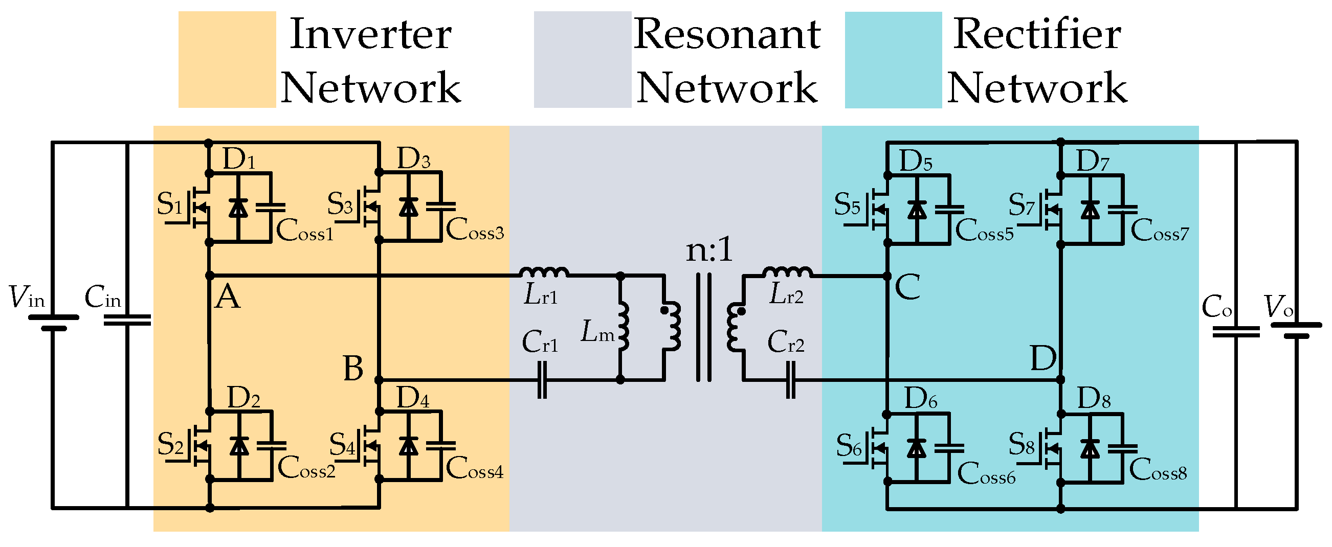
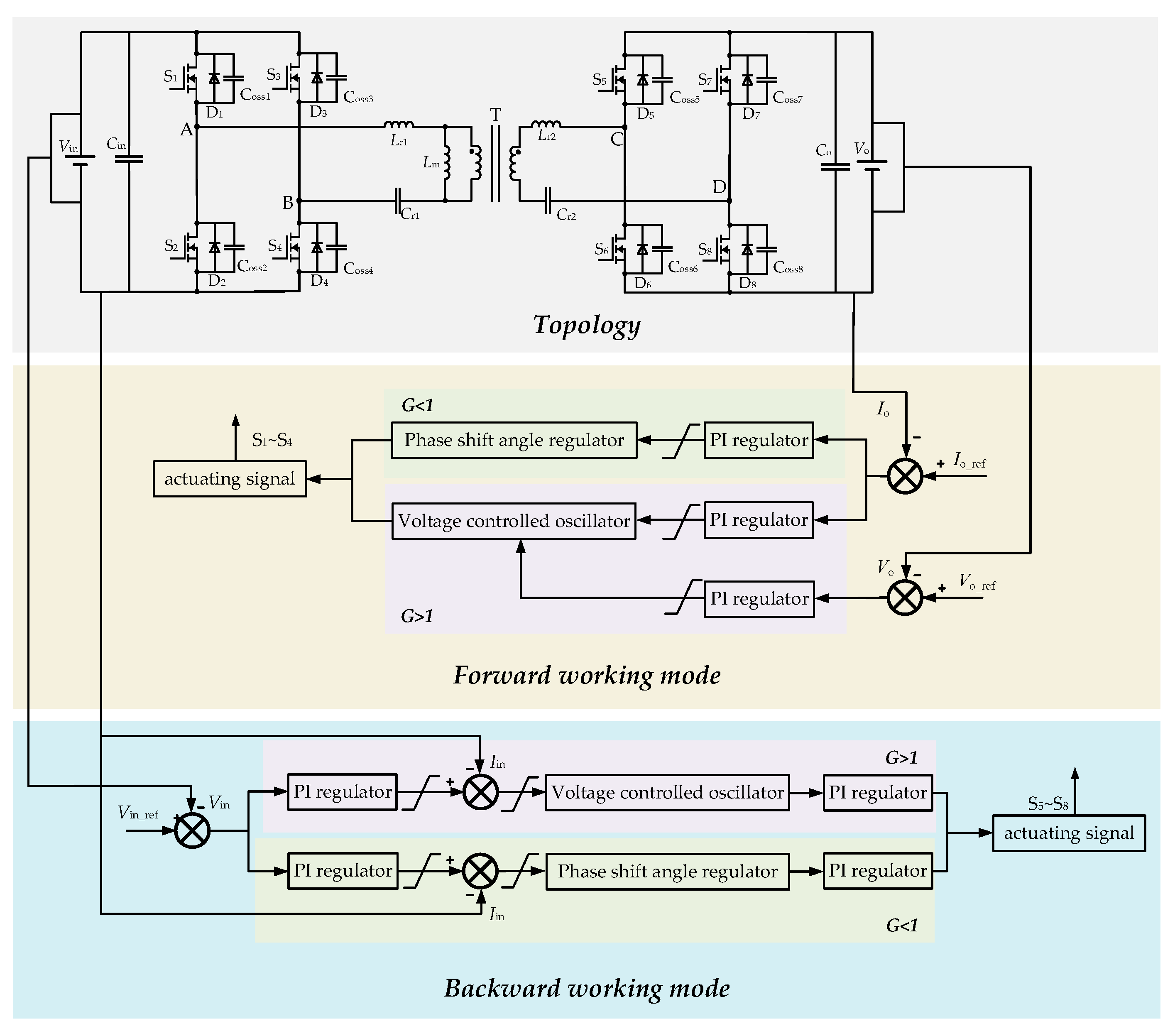
The topology of the bidirectional CLLLC resonant converter is shown in Figure 1. The switching tubes S1~S4 constitute the primary-side full bridge, and S5~S8 constitute the secondary-side full bridge. D1~D8 are the body diodes of S1~S8, and Ccoss1~Ccoss8 are the output capacitors of S1~S8. The ratio of the transformer is n:1; Lm is the excitation inductance of the transformer; Lr1, Lr2, Cr1, and Cr2 are the resonant inductance and resonant capacitance of the primary side and the secondary side, respectively, and the high-frequency transformer is used for electrical isolation. UAB is the primary voltage, UCD is the secondary voltage, and Cin and Co are the filter capacitors. When the converter is working forward, the power is transmitted from UAB to UCD. Since the converter operates in the same state when it is working in the forward and reverse operations, only the positive working time is taken as an example for the analysis.
The left and right sides are full-bridge structures, and the structures are symmetrical to each other. In both the forward and reverse modes, energy can be transferred to achieve a bidirectional flow of energy, and the converter acts as an LLC resonant converter in both the forward and reverse operations. When the converter is working in the forward operation, switches S1~S4 obtain the driving signal to realize the inverter and S5~S8 realize the rectification.
2.2. Working Characteristics of Frequency-Conversion Control
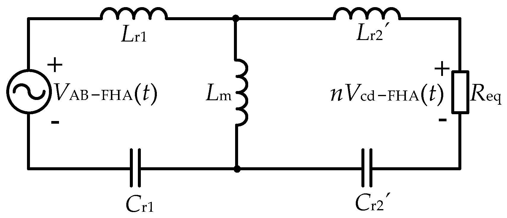
The fundamental analysis method is used to analyze the operating characteristics of the converter, and the fundamental equivalent circuit is shown in Figure 2. Among them, VAB_FHA(t) is the square-wave fundamental component of the input DC-bus voltage after the full-bridge inverter. Lr2′ and Cr2′ are the values of the capacitance and inductance converted from Lr2 and Cr2 to the primary side of the transformer. Req is the equivalent load converted to the primary side. The expression is:
where n is the transformer ratio; Vout, Iout, and Pout are the output voltage, output current, and output power, respectively.
When the voltage at both ends of Lm is clamped by the output voltage, the corresponding resonant frequency is the first resonant frequency:
When Lm is no longer clamped by the output, the corresponding resonant frequency is the second resonant frequency:
We define impedance as follows:
where Z1 is the primary-side series-resonant impedance; Z2 is the equivalent secondary series-resonant impedance; Zm is the excitation inductance impedance; and is the switching angular frequency, .
From Figure 2, the transfer function of the converter is as follows:
By substituting Equation (4) into Equation (5), the voltage gain of the converter can be obtained:
where k is the inductance coefficient, k = Lm/Lr1; Q is the quality factor, ; fn is the normalized frequency; ; and fs is the actual switching frequency.
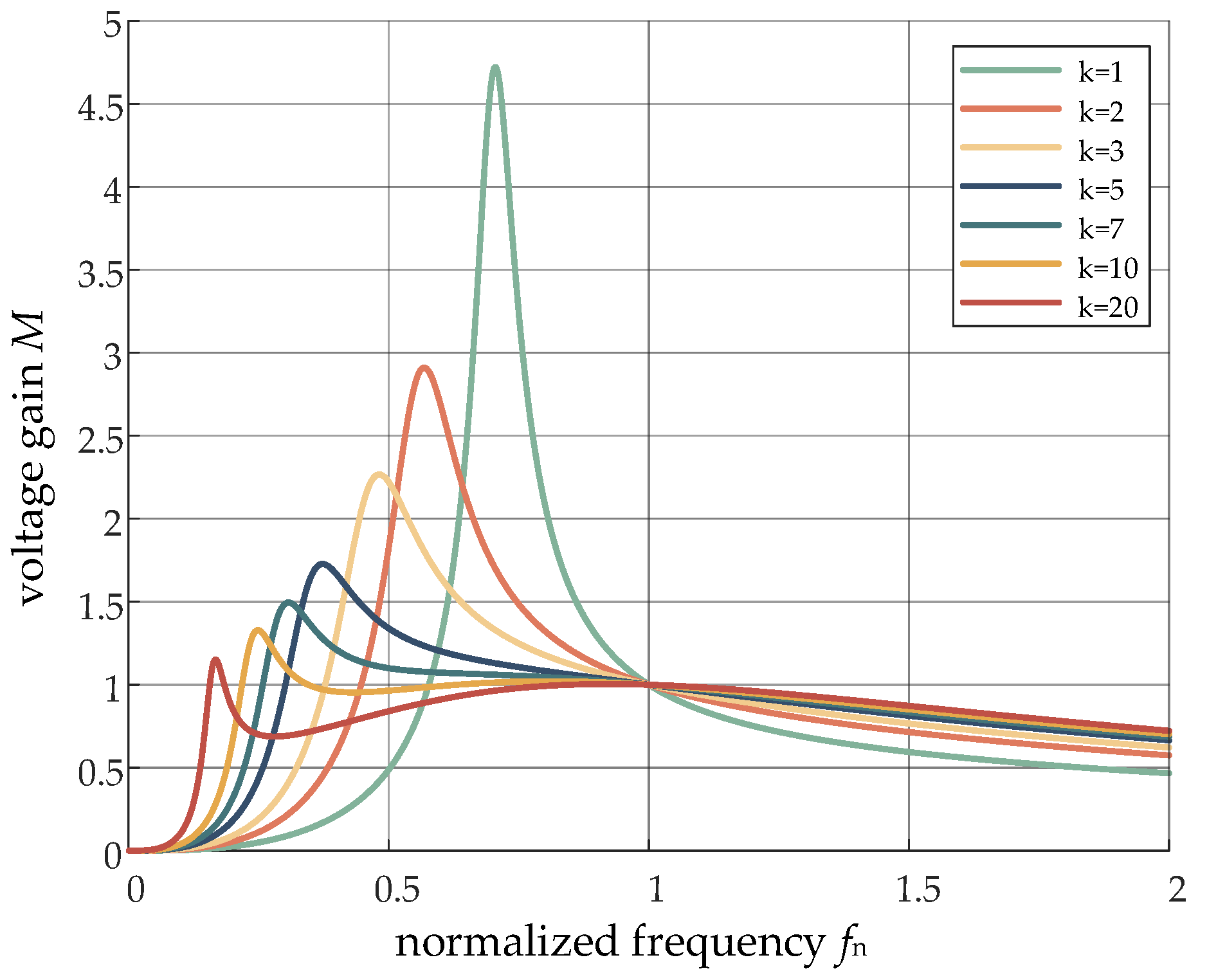
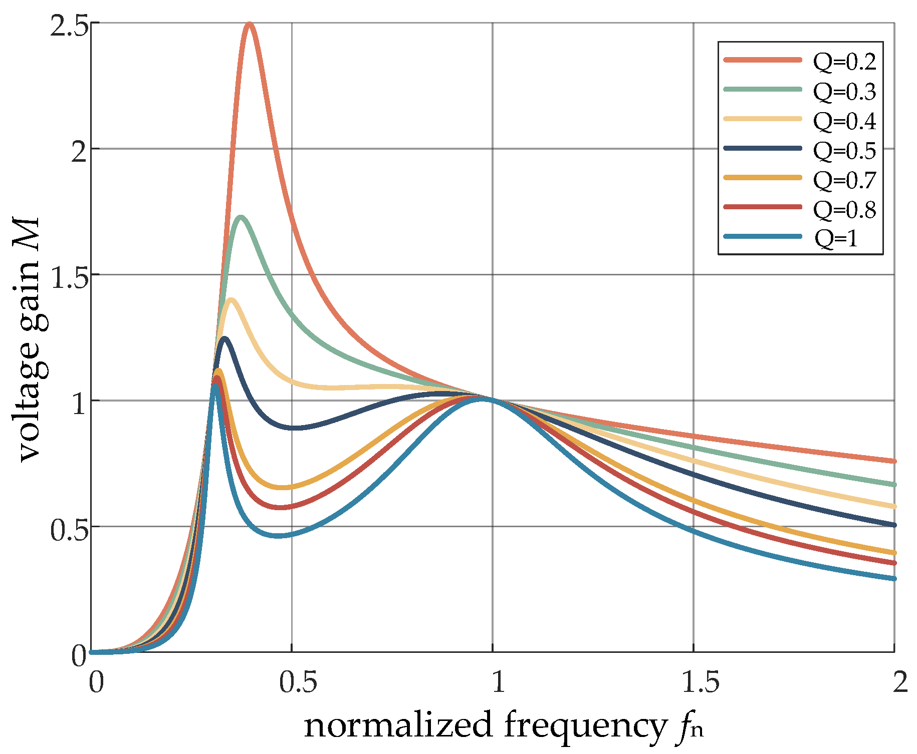
It can be seen from Equation (6) that the voltage gain of the CLLLC resonant converter includes three parameters: the inductance coefficient k, the quality factor Q, and the normalized switching frequency fn. The main parameters affecting the voltage gain are the inductance coefficient k and quality factor Q, which are analyzed in detail below:
- (1)
- Influence of inductance factor k on voltage gain
Figure 3 is the curve of the voltage gain and normalized frequency under different inductance coefficients k when Q = 0.3. When fn = 1, the resonant frequency is equal to the switching frequency, the system works at the resonant point, and no matter how k changes, the voltage gain is always 1. In the under-resonant region, the smaller the k value, the greater the maximum voltage gain, and the narrower the frequency modulation range, which is conducive to the adjustment of the wide gain range. As the k value increases, the peak value of the converter voltage gain gradually decreases, the normalized frequency corresponding to the maximum gain of the curve gradually decreases, and the frequency modulation range becomes wider. In the over-resonant region, the voltage gain curve becomes smooth and the effect of adjusting the voltage gain by adjusting the switching frequency is very limited. If the gain is expected to remain unchanged in a wide range around the resonance point, then k should take a larger value. However, when the k value is greater than a certain value, the peak voltage gain of the converter will be less than the maximum value required by the design, and the minimum switching frequency is too low.
- (2)
- Influence of quality factor Q on voltage gain
Figure 4 shows the curves of the voltage gain and normalized frequency under different quality factors Q when k = 5. When fn = 1, the resonant frequency is equal to the switching frequency, and the system works at the resonant point; no matter how Q changes, the voltage gain is always 1. When the converter is at a light load, that is, the Q value is small, the gain of the converter can be greatly improved when the switching frequency is reduced in the under-resonant region. In the over-resonant region, when the switching frequency increases, the converter gain will only decrease slightly, and the frequency adjustment effect is low. To achieve the effect of voltage regulation, a high frequency is required, and the switching loss increases. Therefore, the selection of the Q value needs to ensure that the converter can meet the requirements of a minimum voltage gain at a light load and that the maximum switching frequency cannot be too high. As the Q value increases, the load becomes heavier and heavier. In the over-resonant region, the gain of the converter changes with the switching frequency. However, when the load is too heavy, the peak value of the maximum gain of the converter decreases in the under-resonant region. To obtain the maximum voltage gain, the switching frequency needs to be reduced to broaden the frequency modulation. The voltage gain curve has two peak points, which are not conducive to the stability of the converter and the design of the control system. Therefore, the selection of the Q value should also be compromised.
For the primary-side switching tube of the converter, after the end of the half-cycle, there is still an inductor current iLr flowing through the resonant circuit, which can discharge and charge the parasitic capacitance Coss of the switching tube. It is assumed that the current flowing through the switching tube remains unchanged as iLr within the dead time td, and the parasitic capacitance Coss of the switching tube is equal. To achieve ZVS conditions, iLr must be greater than the minimum current for charging and discharging Coss during the dead time, that is:
2.3. Working Characteristics of Phase-Shift Control
When the converter adopts phase-shift control, due to the introduction of the phase-shift angle , the voltage of the input resonant cavity UAB changes from a square wave with a duty cycle of 50% to a square wave with a duty cycle of less than 50% and a zero level. From the fundamental equivalent model and Fourier analysis shown in Figure 2, the fundamental component of the input voltage square wave under phase-shift control is expressed as:
where D is the phase shift, , ; and is the phase-shift angle.
Combining Equations (5)–(8), the voltage gain expression under phase-shift control is:
It can be seen that the voltage gain is approximately cosine with D, and the variation range is between 0 and 1.
In the period, the Lm2 two-terminal voltage is U2. From and Equation (7), it is necessary to ensure that the voltage at both ends of Coss meets in the dead time td to achieve soft switching. Further, the conditions for soft switching under phase-shift control are:
3. Resonant Network Parameter Design
The design specifications of the bidirectional CLLLC resonant converter are shown in Table 1.
- (1)
- Turn ratio of transformer n
At the resonant frequency point of the bidirectional resonant converter, the voltage gain of the converter is always 1, which is independent of the change of the circuit parameters and the load. The rated operating point is usually set here, so the turn ratio n of the transformer is:
- (2)
- Transformer normalized voltage gain M
The normalized maximum voltage gain of this converter is:
The normalized minimum voltage gain of this converter is:
- (3)
- Parameter design of inductance coefficient k and quality factor Q
Because the phase-shift control mode is adopted in the output low voltage, the limit condition of k is no longer applicable to the no-load condition of the minimum output voltage corresponding to the highest input voltage in the traditional design method. Considering that the maximum output voltage corresponding to the lowest input voltage is fully loaded as the limit condition of the k value, the range of the inductance coefficient is:
Although increasing the k value can reduce the loss of the loop, it will increase the range of the switching frequency. In combination with Equation (14) and Figure 3, we finally choose k = 5.
In combination with Equation (15) and Figure 4, Q = 0.3 is selected. At this time, the requirements of maximum gain and minimum gain can be met by smaller frequency adjustments, and the monotonicity can be maintained.
- (4)
- Design of resonant inductor and resonant capacitor
The equivalent impedance of the converter is:
According to Equation (8) through Equation (16), the parameters of the primary and secondary resonant inductors and resonant capacitors can be obtained, as shown in Table 2.
4. Frequency-Conversion and Phase-Shift Hybrid Control Strategy
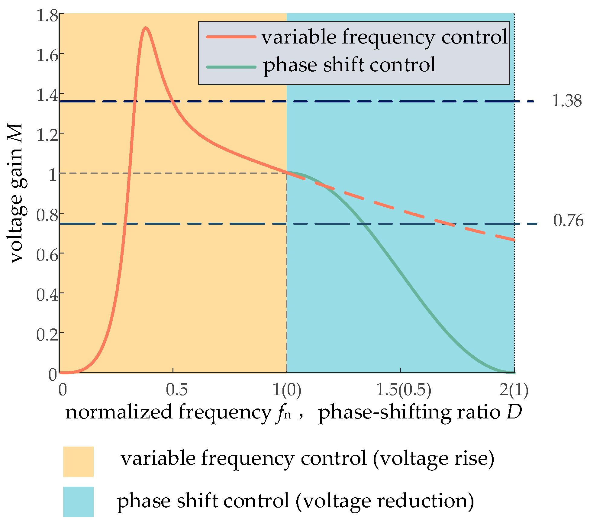
Combining Equations (6), (9), and (10), the relationship curve of the voltage gain with the normalized frequency fn (under frequency-conversion control) and the phase-shift ratio D (under phase-shift control) can be obtained, as shown in Figure 5. After the quality factor is selected as 0.3, when the bidirectional CLLLC resonant converter is controlled by frequency conversion alone, the voltage gain range is narrow in the step-down mode, and the switching frequency needs to change greatly to change the voltage gain. When phase-shift control is used alone, the maximum voltage gain is only 1, which can only be realized in the step-down mode. The minimum voltage gain in the phase-shift mode is much smaller than the minimum voltage gain under frequency-conversion control. Therefore, this paper proposes a method of frequency-conversion and phase-shift hybrid control applied to a bidirectional CLLLC resonant converter to broaden the voltage gain range. At the resonance point, the working conditions of frequency-conversion control and phase-shift control are the same. Setting this as a switching point can achieve a seamless connection of the voltage gain; that is, frequency-conversion control is adopted when M > 1, and phase-shift control is adopted when M < 1.
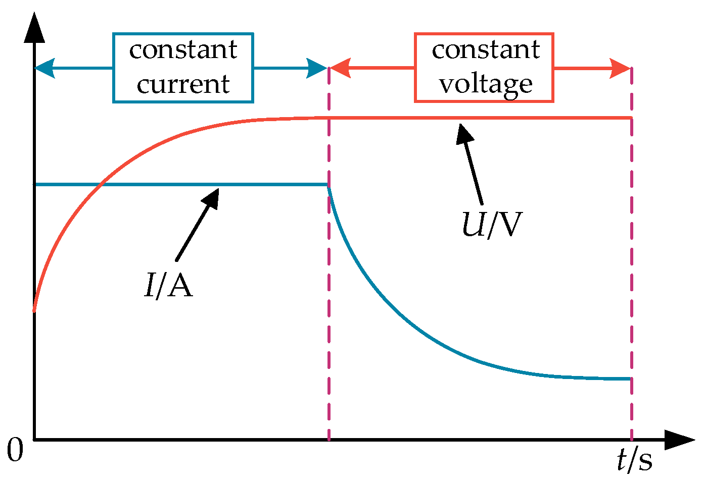
The bidirectional CLLLC resonant converter designed in this paper is applied to the rear stage of the vehicle charger. The charging process of the charging vehicle generally has two stages: constant current charging and constant voltage charging. The charging curve is shown in Figure 6. The first stage is the constant-current-charging stage. At this stage, a certain constant current is used for constant current charging. The voltage values of the battery are relatively small at the beginning, far less than the set value. The voltage loop is always saturated. At this time, only the current loop plays a regulatory role. The voltage value continues to rise during the charging process. When the voltage rises to the set value, it enters the second stage. The second stage is the constant-voltage-charging stage. At this stage, the voltage loop exits the saturation state and the output value begins to decrease. Until it is lower than the output value of the current loop regulator, it begins to be regulated by the voltage loop and enters the constant-voltage-charging stage. At this time, the current loop is saturated, and the charging current begins to decrease gradually until the charging current of the battery is equal to the self-discharge current, and the whole charging process ends.
Figure 7 is the control block diagram of using the frequency-conversion and phase-shift hybrid control mode. In the whole control process, the load uses the resistance load, and the output voltage and current are sampled as the judgment basis. To realize the automatic switching of the constant current and constant voltage loop, the voltage loop and the current loop are controlled in parallel when working forward. Comparing the actual battery voltage value obtained by sampling with the set value Uref, the constant-current-control mode is selected when the battery voltage is less than the set value Uref, and the constant-voltage-control mode is selected when the battery voltage reaches the set value Uref. When working in the reverse direction, the voltage and current double-closed-loop control method are adopted to output the electric energy in the battery to the primary side through the resonant cavity to obtain a stable 400 V voltage.
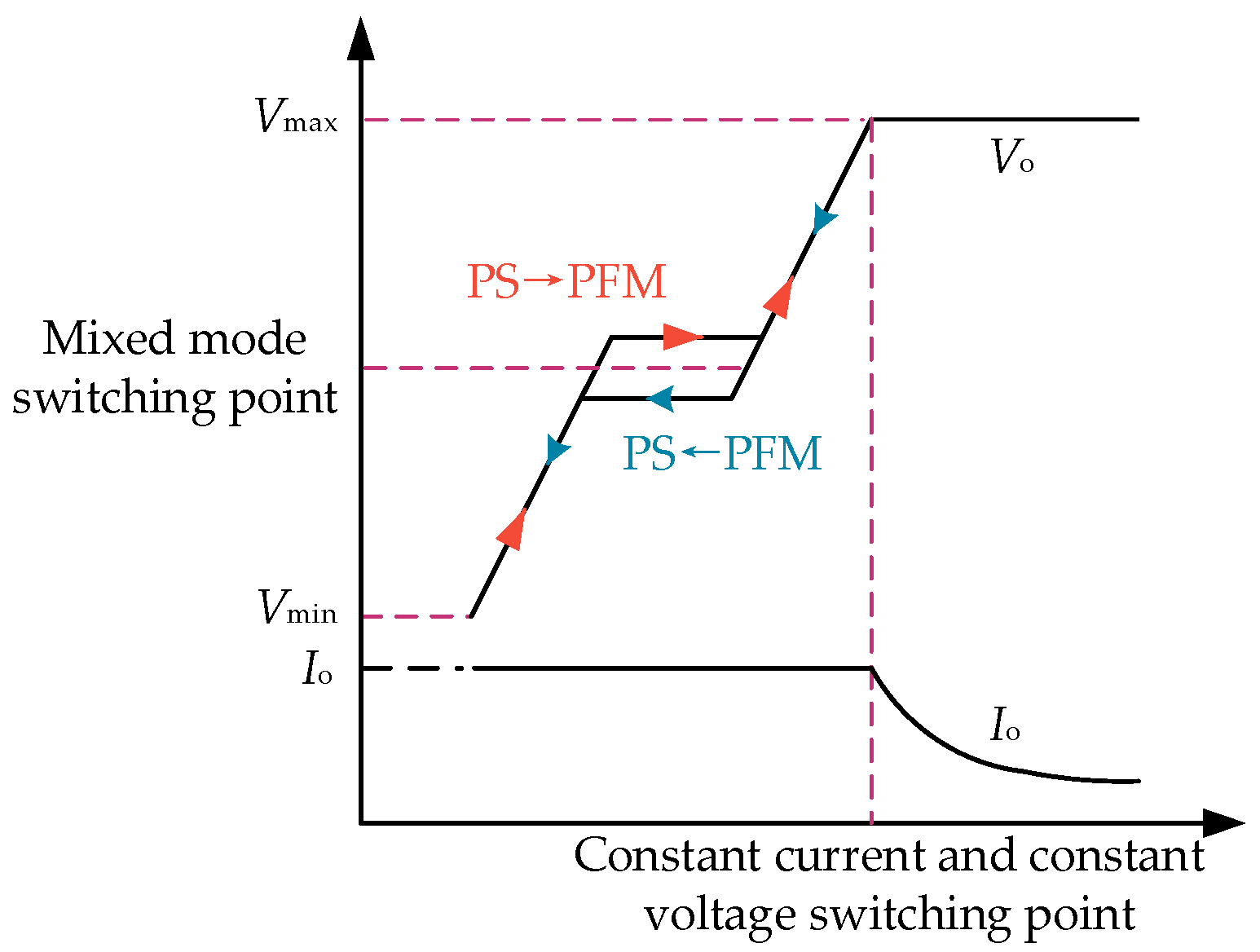
Figure 8 is the hysteresis-control-switching diagram of the bidirectional CLLLC resonant converter. This paper uses the two control modes of frequency-conversion control and phase-shift control. In order to avoid unstable oscillation, the switching of these two modes should be set to hysteresis control, rather than switching at a single point. When the voltage rises to the maximum set value of phase-shift control, it is switched to frequency-conversion control. When the voltage drops to the minimum set value of frequency-conversion control, phase-shift control is switched. When setting the value of the mode-switching point, the maximum setting value of phase-shift control is higher than the minimum setting value of frequency-conversion control. The existence of the buffer region can make the converter switch reliably between the two control modes.
5. Simulation Analysis
5.1. Forward Simulation
When the converter is working in the forward direction, the input voltage remains unchanged at 400 V, and the output voltage is gradually increased from 250 V to 430 V by adjusting the phase-shift angle between S1 and S2, and S4 and S3, or adjusting the switching frequency of S1, S2, S3, and S4. In Figure 9, Figure 10 and Figure 11, Vgs and Vds represent the driving signal and drain-source voltage of the corresponding switching tube, respectively. iD represents the forward current of the rectifier diode D, VAB is the resonant slot input voltage, iLr is the resonant current, and iLm is the excitation inductance current.
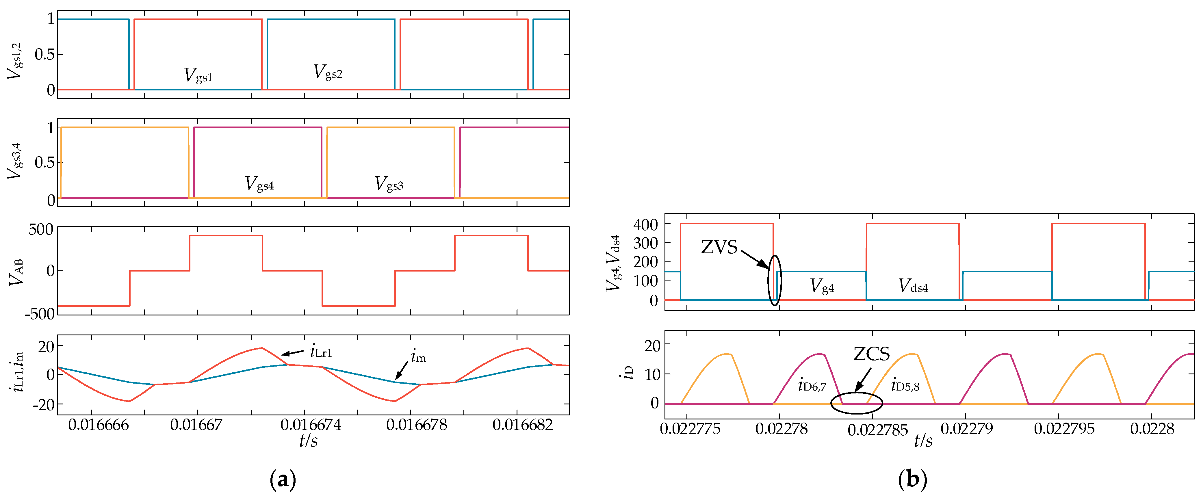
Figure 9 shows the simulation results when the output voltage Vo and the output current Io are 250 V/7.67 A in the constant current mode. At this time, the output power Po = 1917.5 W, which is the lightest working point of the converter during the constant current operation. It can be seen from Figure 9a that the converter operates in phase-shift mode, and the output voltage is controlled by adjusting the phase-shift angle between S1 and S4, and S2 and S3. It can be seen from Figure 9b that the drain voltage Vds4 of S4 has been reduced to zero before the arrival of the driving signal Vgs4 of the switching tube S4. It can be seen that the primary-side switch can achieve ZVS. Before the arrival of iD5 and iD8, iD6 and iD7 have been reduced to zero. Similarly, before the arrival of iD6 and iD7, iD5 and iD8 have also been reduced to zero, so the secondary rectifier diode can achieve ZCS.
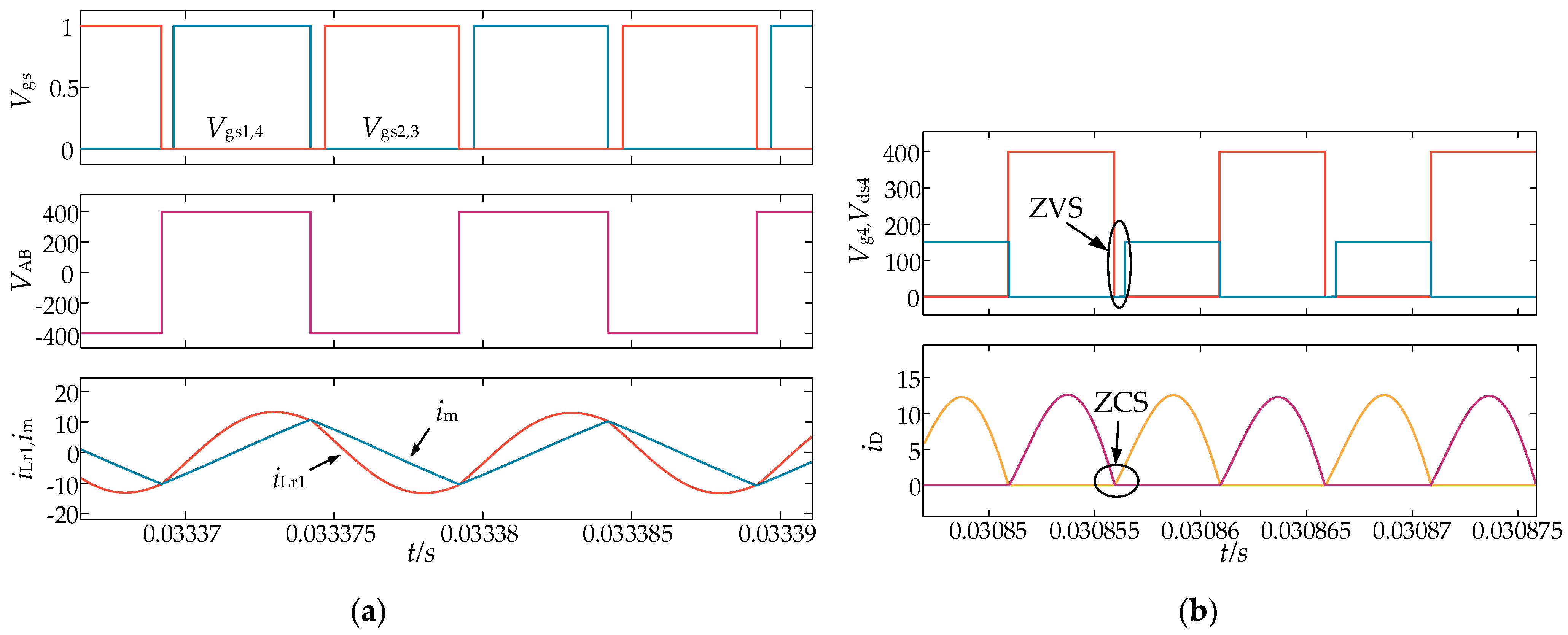
Figure 10 shows the simulation results of the converter in the constant current mode when the output voltage Vo and the output current Io are 320 V/7.67 A. At this time, the output power Po = 2454.4 W. As can be seen from Figure 10a, the converter works in the frequency-conversion mode, the switching frequency is 100 kHz, and the primary-side resonant current changes in the form of a sine wave. At this time, the converter works at the rated operating point and is in a quasi-resonant state. It can be seen from Figure 10b that before the arrival of the driving signal Vgs4 of the switching tube S4, the drain voltage Vds4 of S4 has dropped to zero, which shows that the primary-side switching tube can achieve ZVS. Since the resonant current and the excitation current are equal only for a moment, iD6 and iD7 are generated at the moment iD5 and iD8 are reduced to zero. Similarly, iD5 and iD8 are generated at the moment when iD6 and iD7 are reduced to zero, so the secondary rectifier diode can achieve ZCS.
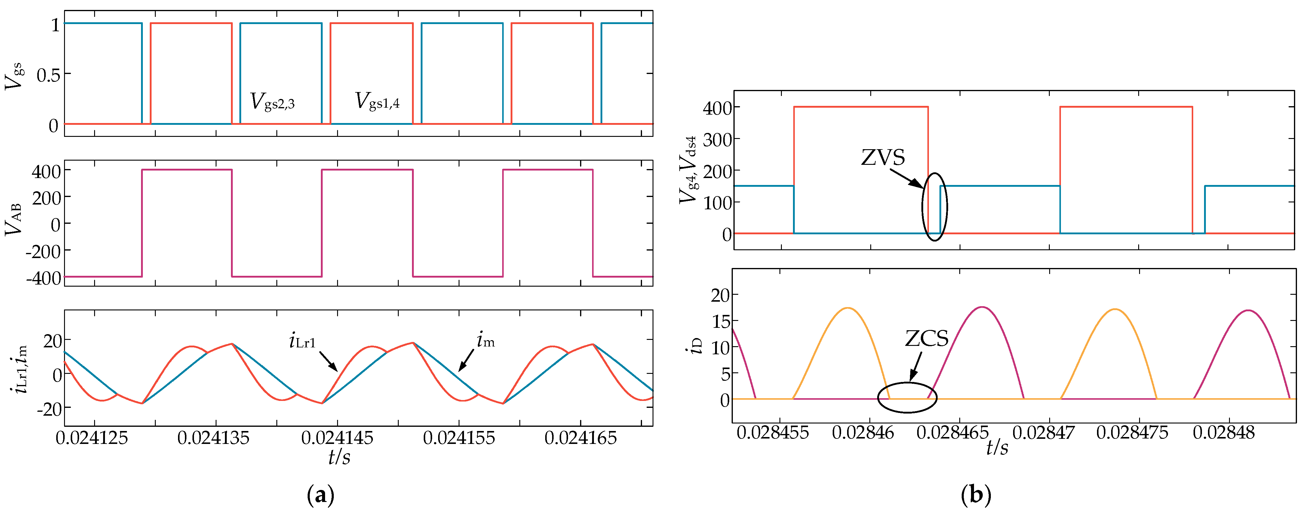
Figure 11 shows the simulation results when the output voltage Vo and the output current Io are 430 V/7.67 A. At this time, the output power Po = 3300 W. It can be seen from Figure 11a that the converter works in the frequency-conversion mode, and the switching frequency is 67 kHz. At this time, the converter works in an under-resonant state. It can be seen from Figure 11b that the primary-side switch can achieve ZVS, and the secondary-side rectifier diode can achieve ZCS.
To verify the performance of the proposed bidirectional CLLLC resonant converter under constant current and constant voltage charging, the closed-loop simulation of the converter is carried out. The simulation results are shown in Figure 12 and Figure 13.
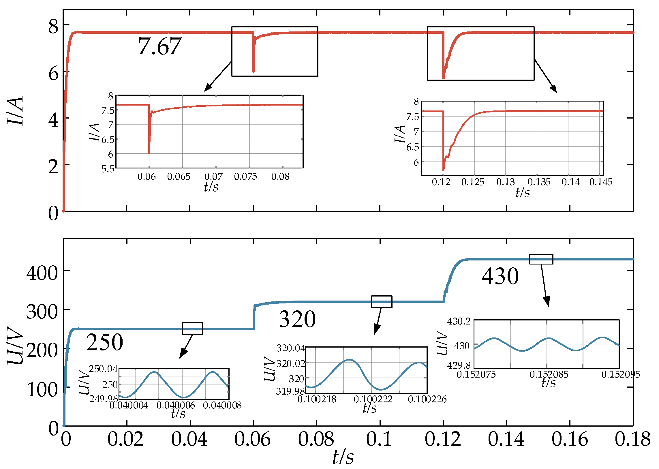
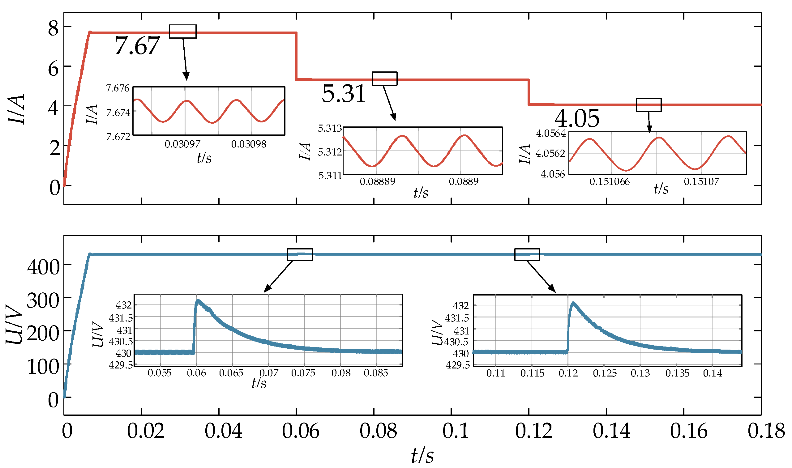
Figure 12 is the closed-loop simulation waveform of the converter in the constant current stage. When the converter is in the constant current stage, the voltage loop is saturated. At this time, the current loop works. The output current remains constant at 7.67 A throughout the constant current stage, and the output voltage rises from 250 V to 430 V. At the beginning of the simulation, the load is set to 32.59 Ω. Before the simulation time reaches 0.06 s, the output current remains 7.67 A, and the output voltage quickly reaches and can be stabilized at 250 V. At 0.06 s, the load changes from 32.59 Ω to 41.72 Ω. Due to the existence of the filter capacitor, the output voltage does not change immediately, and the output current drops sharply. After about 13 ms, the output current is stable at 7.67 A, and the output voltage reaches 320 V. At 0.12 s, the load changes from 41.72 Ω to 56.03 Ω at full load. After a sharp drop, the output current is stabilized at 7.67 A after about 8 ms, and the output voltage finally reaches and stabilizes at 430 V. The above process proves that the converter can work normally in the constant current stage.
Figure 13 is the closed-loop simulation waveform of the converter in the constant voltage stage. In the constant voltage stage, the current loop of the converter is saturated, and the voltage loop works at this time. The output voltage remains constant at 430 V throughout the constant voltage stage, and the output current gradually decreases from 7.67 A to equal to the self-discharge current. At the beginning of the simulation, the load is set to 56.03 Ω. Before the simulation time reaches 0.06 s, the output voltage remains constant at 430 V and the output current remains at 7.67 A. At 0.06 s, the load changes from 56.03 Ω to 81.03 Ω. Due to the existence of the voltage closed-loop regulation, the output voltage fluctuates slightly, and the output current drops sharply to 5.31 A. At 0.12 s, the load changes from 81.03 Ω to 106.03 Ω, and the output current drops sharply to 4.05 A. The two output voltages are quickly restored to stability after the oscillation, and the ripple is within 0.6%. The above process proves that the converter can work normally in the constant voltage stage.
5.2. Reverse Simulation
When the bidirectional CLLLC resonant converter is in the reverse discharge mode, the input voltage range is 250 V~430 V, and the voltage and current double-closed-loop control mode is adopted to control the output voltage to be stable at 400 V DC. The magnetizing inductance is equivalent to the secondary side, and the magnetizing inductance is Lm/n2 = 60.03 .
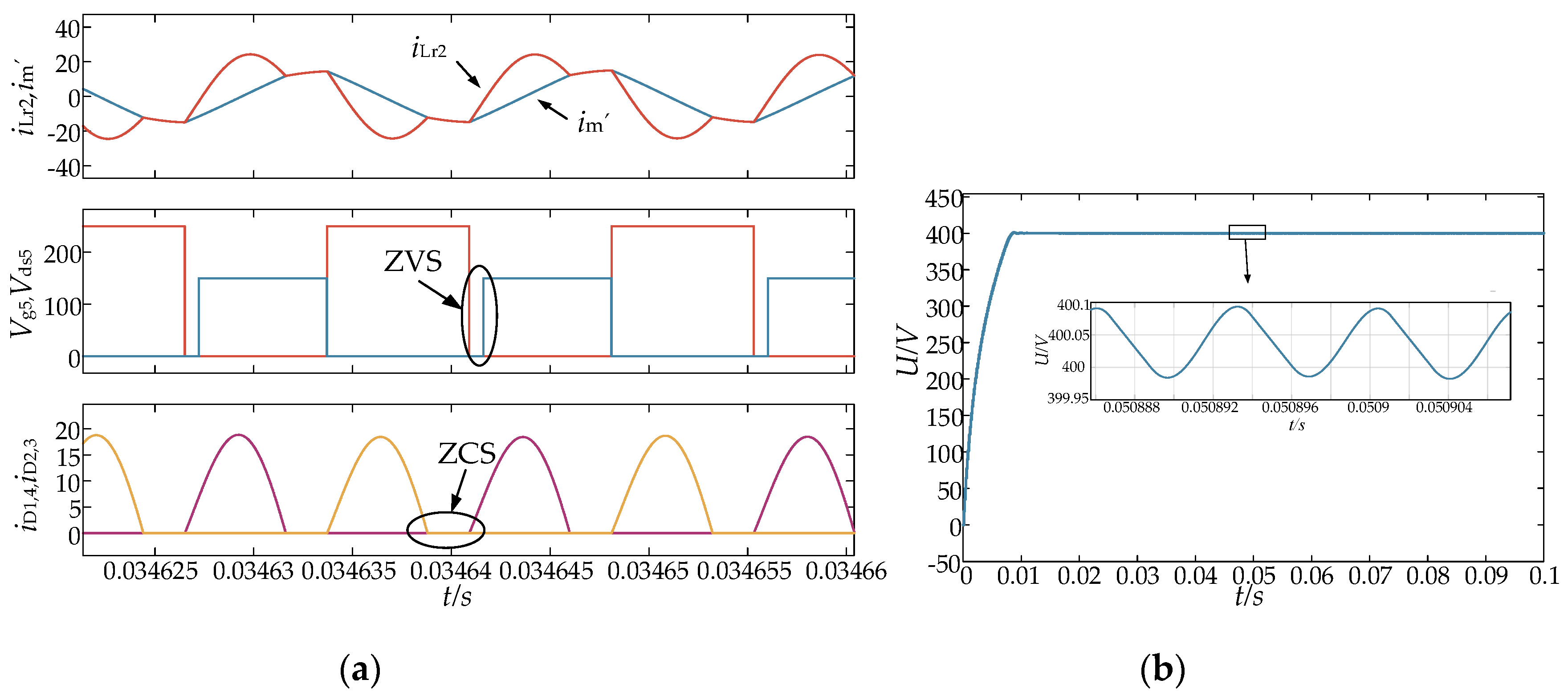
Figure 14 is the simulation result when the reverse input voltage is 250 V. As can be seen from Figure 14a, at this time in the variable-frequency-boost mode, the operating frequency is 69 kHz. Before the arrival of the driving signal Vgs5 of the switching tube S5, the drain voltage Vds5 of the S5 has been reduced to zero, which shows that the switching tube S5 can achieve ZVS. Before the arrival of iD1 and iD4, iD2 and iD3 have been reduced to zero. Similarly, before the arrival of iD2 and iD3, iD1 and iD4 have also been reduced to zero, so the rectifier diode on the primary side can achieve ZCS. It can be seen from Figure 14b that the output voltage is stable at 400 V after 8 ms, indicating that the reverse frequency-conversion boost of the bidirectional CLLLC resonant converter can work normally.
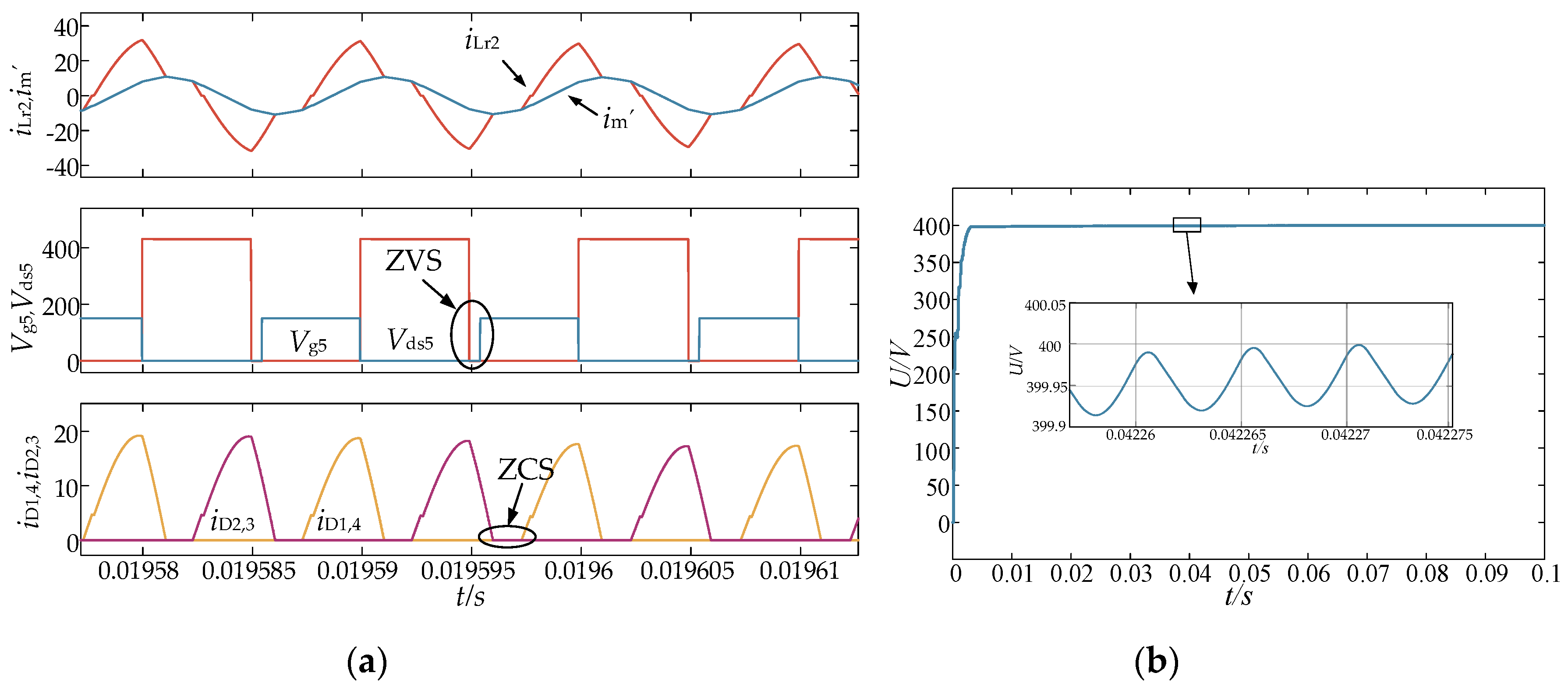
Figure 15 is the simulation result when the reverse input voltage is 450 V. As can be seen from Figure 15a, it is in the phase-shift buck mode, and the operating frequency is 100 kHz. Before the arrival of the driving signal Vgs5 of the switching tube S5, the drain voltage Vds5 of the S5 has been reduced to zero, which shows that the switching tube S5 can achieve ZVS. Before the arrival of iD1 and iD4, iD2 and iD3 have been reduced to zero. Similarly, before the arrival of iD2 and iD3, iD1 and iD4 have also been reduced to zero, so the rectifier diode on the primary side can achieve ZCS. From Figure 15b, it can be seen that the output voltage is stable at 400 V after 2.9 ms, indicating that the reverse phase-shift buck of the bidirectional CLLLC resonant converter can work normally.
6. Conclusions
To meet the requirements of the on-board charging equipment of electric vehicles, this paper adopts the bidirectional CLLLC resonant converter as the rear stage of the on-board charger and analyzes the characteristics of this converter under frequency-conversion control and phase-shift control, and proposes a hybrid method of frequency-conversion and phase-shift control. Through the above analysis, the following conclusions can be drawn:
- (1)
- Due to its complete symmetrical and good soft-switching characteristics, the bidirectional CLLLC resonant converter solves the problem where the traditional LLC resonant converter has different resonant states during the forward and reverse operations, and cannot achieve soft switching at the same time and is difficult to control.
- (2)
- The hybrid control method of frequency conversion and phase shift adopts frequency-conversion control at a higher voltage gain and phase-shift control at a lower voltage gain. It solves the problem of low voltage gain of the single frequency-conversion control method in the step-down mode, effectively broadens the output voltage range of the bidirectional CLLLC converter, and is suitable for wide-range output occasions. At the same time, it achieves zero-voltage switching and zero-current switching in the full load range, and has a high operating efficiency. This control method is convenient and easy to implement.
- (3)
- The control method proposed in this paper is superior to the traditional control method in reducing the switching frequency-conversion range and improving the efficiency of the converter, which is helpful in the popularization and application of the high-efficiency and high-power bidirectional DC/DC converter in the distributed new energy generation.
- (4)
- In the actual debugging process, it is difficult to establish an accurate model of a bidirectional CLLLC circuit. In the later stage, it is necessary to further analyze the circuit model to design more appropriate closed-loop control parameters and test how well it actually works.
Author Contributions
Conceptualization, N.-Z.J. and Y.F.; methodology, N.-Z.J. and Y.F.; software, Y.F. and Z.-Y.C.; validation, Y.F. and Z.-Y.C.; supervision, N.-Z.J. and X.-G.W.; writing—original draft, Y.F.; writing—review and editing, N.-Z.J., Y.F. and X.-G.W. All authors have read and agreed to the published version of the manuscript.
Funding
This research was funded by the Open Fund Project of the State Key Laboratory of Automotive Safety and Energy, grant number KFY2222.
Data Availability Statement
The data presented in this study are available in the article.
Conflicts of Interest
The authors declare no conflict of interest. The funders had no role in the design of the study; in the collection, analysis, or interpretation of data; in the writing of the manuscript; or in the decision to publish the results.
References
- Wang, D.Y.; Zhao, Q.L.; Li, J. Wide Output Range Multi-Level LLC Resonant Converter with Fixed-Frequency. Chin. J. Electr. Eng. 2022, 43, 1973–1984. [Google Scholar] [CrossRef]
- Yu, W.H.; Guo, Y.; Shang, Z.; Zhang, Y.C.; Xu, S.M. A Review on Comprehensive Recycling of Spent Power Lithium-ion Battery in China. eTransportation 2022, 11, 100155. [Google Scholar] [CrossRef]
- Li, H.M.; Zhang, H.G.; Cui, C. Review of PWM Soft-Switching DC-DC Converter for on-Board Chargers. Chin. J. Electr. Eng. 2017, 32, 59–70. [Google Scholar]
- Ding, C.; Li, Y.; Jiang, L.; Wan, J.H.; Liu, F. Analysis of Soft Switching Voltage Boundary of LLC Resonant Converter for EV DC Charging System. Trans. China Electrotech. Soc. 2022, 37, 3–11. [Google Scholar]
- Wang, Y.J.; Wang, L.; Mince, L.; Chen, Z.H. A review of Key Issues for Control and Management in Battery and Ultra-capacitor Hybrid Energy Storage Systems. eTransportation 2022, 4, 100064. [Google Scholar] [CrossRef]
- Esteban, F.D.; Serra, F.M.; De Angelo, C.H. Control of a DC-DC Dual Active Bridge Converter in DC Microgrids Applications. IEEE Lat. Am. Trans. 2021, 19, 1261–1269. [Google Scholar] [CrossRef]
- Xiong, F.; Wu, L.; Liu, Z.; Hao, L. Current Sensorless Control for Dual Active Bridge DC/DC Converter with Estimated Load-Current Feedforward. IEEE Trans. Power Electron. 2018, 33, 3552–3566. [Google Scholar] [CrossRef]
- Li, X.; Li, Y.F. An Optimized Phase-Shift Modulation for Fast Transient Response in a Dual-Active-Bridge Converter. IEEE Trans. Power Electron. 2014, 29, 2661–2665. [Google Scholar]
- Bal, S.; Yelaverthi, D.B.; Rathore, A.K.; Srinivasan, D. Improved Modulation Strategy Using Dual Phase Shift Modulation for Active Commutated Current-Fed Dual Active Bridge. IEEE Trans. Power Electron. 2018, 33, 7359–7375. [Google Scholar] [CrossRef]
- Guan, Q.X.; Zhang, Y.; Zhao, P.H.; Kang, Y. Zero-voltage Soft-switching Conditions and Loss Balance Method of Three Level ANPC-DAB. Proc. CSEE 2021, 41, 4603–4616. [Google Scholar]
- Hu, Y.; Zhang, T.H.; Yang, L.X.; Guan, X.Q. Comparative Study of Reactive Power Optimization and Current Stress Optimization of DAB Converter with Dual Phase Shift Control. Proc. CSEE 2020, 40, 243–253. [Google Scholar]
- Peiwen, H.E.; Mallik, A.; Sankar, A. Design of a 1-MHz High-efficiency High-power-density Bidirectional GaN-based CLLC Converter for Electric Vehicles. IEEE Trans. Veh. Technol. 2019, 68, 213–223. [Google Scholar]
- Kim, K.; Youn, H.; Baek, J.; Jeong, Y.; Moon, G. Analysis on Synchronous Rectifier Control to Improve Regulation Capability of High-frequency LLC Resonant Converter. IEEE Trans. Power Electron. 2018, 33, 7252–7259. [Google Scholar]
- Yuan, Y.S.; Lai, L. A Compound Resonant Full-bridge Converter Suitable for Wide Range Output. Proc. CSEE 2020, 40, 6694–6704. [Google Scholar]
- Zhu, H.Y.; Zhuo, F.; Zhao, F.Z.; Wang, F. Analysis and Design of Multiple Phase-shift Control for CLLC Resonant Converter Under Light-load Conditions Based on Multi-harmonic Impedance Model. Proc. CSEE 2021, 41, 326–339. [Google Scholar]
- Zhao, L.; Pei, Y.Q.; Liu, X.H.; Fang, W.J. Design Methodology of CLLC Resonant Converters for Electric Vehicle Battery Chargers. Proc. CSEE 2020, 40, 4965–4977. [Google Scholar]
- Mumtahina, U.; Wolfs, P.J. Multimode Optimization of the Phase-shifted LLC Series Resonant Converter. IEEE Trans. Power Electron. 2018, 33, 10478–10489. [Google Scholar] [CrossRef]
- Jiang, T.; Zhang, J.; Wu, X.; Sheng, K.; Wang, Y. A Bidirectional LLC Resonant Converter with Automatic Forward and Backward Mode Transition. IEEE Trans. Power Electron. 2015, 30, 757–770. [Google Scholar] [CrossRef]
- Yuan, Y.S.; Lai, L. A Multi-mode Current-fed LCL Resonant Converter. Proc. CSEE 2020, 40, 3259–3270. [Google Scholar]
- Zuo, Y.; Pan, X.; Wang, C. A Reconfigurable Bidirectional Isolated LLC Resonant Converter for Ultra-Wide Voltage-Gain Range Applications. IEEE Trans. Ind. Electron. 2022, 69, 5713–5723. [Google Scholar] [CrossRef]
- Sun, X.N.; Chen, M.; Li, B.D.; Zhang, D.B.; Wang, X.Q. Efficiency Optimization of CLLC Resonant Converter Based on Analysis of the Ratio of Inductances. Proc. CSEE 2021, 41, 2825–2834. [Google Scholar]
- Wei, Y.; Luo, Q.; Mantooth, H.A. An LLC and LCL-T Resonant Tanks Based Topology for Battery Charger Application. CPSS Trans. Power Electron. Appl. 2021, 6, 263–275. [Google Scholar] [CrossRef]
- Liu, B.L.; Zhang, X.D.; Li, Y.; Wu, W. Variable Frequency-phase Shift Control Method for LLC Resonant Converter Applied to Electric Vehicle Charging. J. Power Supply 2020, 18, 43–52. [Google Scholar]
- Pan, J.; Shi, D.; Liu, S.L. Wide Output Dual Full Bridge LLC Resonant Converter with Hybrid Control Strategy. J. Power Supply 2023, 1–16. Available online: http://kns.cnki.net/kcms/detail/12.1420.TM.20220307.1010.004.html (accessed on 28 February 2023).
- Tao, W.D.; Wang, Y.B.; Zhang, F.Y. Pulse Frequency Modulation and Phase Shift Combined Control Method for Bidirectional LLC Resonant Converter. Trans. China Electrotech. Soc. 2018, 33, 5856–5863. [Google Scholar]
- Liu, T.; Yang, X.-G.; Ge, S.; Leng, Y.; Wang, C.-Y. Ultrafast Charging of Energy-dense Lithium-ion Batteries for Urban Air Mobility. eTransportation 2021, 7, 100103. [Google Scholar] [CrossRef]
Figure 1.
Bidirectional CLLLC resonant converter.

Figure 2.
Forward equivalent circuit model of bidirectional CLLLC resonant converter.

Figure 3.
Voltage gain and normalized frequency at different k values when Q = 0.3.

Figure 4.
Voltage gain and normalized frequency at different Q values when k = 5.

Figure 5.
Voltage gain under frequency-conversion–phase-shift control.

Figure 6.
Constant-current- and constant-voltage-charging curve.

Figure 7.
Mixed control block diagram.

Figure 8.
Hysteretic-control-switching diagram.

Figure 9.
The simulated waveform of Vo and Io is 250 V/7.67 A: (a) main working waveform; and (b) ZVS and ZCS.
Figure 9.
The simulated waveform of Vo and Io is 250 V/7.67 A: (a) main working waveform; and (b) ZVS and ZCS.

Figure 10.
The simulated waveform of Vo and Io is 320 V/7.67 A: (a) main working waveform; and (b) ZVS and ZCS.
Figure 10.
The simulated waveform of Vo and Io is 320 V/7.67 A: (a) main working waveform; and (b) ZVS and ZCS.

Figure 11.
The simulated waveform of Vo and Io is 430 V/7.67 A: (a) main working waveform; and (b) ZVS and ZCS.
Figure 11.
The simulated waveform of Vo and Io is 430 V/7.67 A: (a) main working waveform; and (b) ZVS and ZCS.

Figure 12.
Simulation waveform of forward constant-current stage.

Figure 13.
Simulation waveform of forward constant-voltage stage.

Figure 14.
Simulation results when the reverse input voltage is 250 V: (a) main working waveform; and (b) output voltage.
Figure 14.
Simulation results when the reverse input voltage is 250 V: (a) main working waveform; and (b) output voltage.

Figure 15.
Simulation results when the reverse input voltage is 430 V: (a) main working waveform; and (b) output voltage.
Figure 15.
Simulation results when the reverse input voltage is 430 V: (a) main working waveform; and (b) output voltage.


Table 1.
Design specifications of bidirectional CLLLC resonant converter.
| Main Indicator | Parameter |
|---|---|
| input voltage range | 390–410 V |
| rated input voltage | 400 V |
| output voltage range | 250–430 V |
| rated output voltage | 320 V |
| maximal output power | 3.3 kW |
| resonant frequency | 100 kHz |
Table 2.
The parameters of primary and secondary resonant inductance and resonant capacitance.
| Main Indicator | Parameter |
|---|---|
| primary-side resonant inductor (Lr1) | 18.76 |
| primary-side resonant capacitor (Cr1) | 135.02 |
| secondary-side resonant inductance (Lr2) | 12.01 |
| secondary-side resonant capacitor (Cr2) | 210.97 |
| magnetizing inductance (Lm) | 93.80 |
Disclaimer/Publisher’s Note: The statements, opinions and data contained in all publications are solely those of the individual author(s) and contributor(s) and not of MDPI and/or the editor(s). MDPI and/or the editor(s) disclaim responsibility for any injury to people or property resulting from any ideas, methods, instructions or products referred to in the content. |
© 2023 by the authors. Licensee MDPI, Basel, Switzerland. This article is an open access article distributed under the terms and conditions of the Creative Commons Attribution (CC BY) license (https://creativecommons.org/licenses/by/4.0/).
Share and Cite
MDPI and ACS Style
Jin, N.-Z.; Feng, Y.; Chen, Z.-Y.; Wu, X.-G. Bidirectional CLLLC Resonant Converter Based on Frequency-Conversion and Phase-Shift Hybrid Control. Electronics 2023, 12, 1605. https://doi.org/10.3390/electronics12071605
AMA Style
Jin N-Z, Feng Y, Chen Z-Y, Wu X-G. Bidirectional CLLLC Resonant Converter Based on Frequency-Conversion and Phase-Shift Hybrid Control. Electronics. 2023; 12(7):1605. https://doi.org/10.3390/electronics12071605
Chicago/Turabian StyleJin, Ning-Zhi, Yu Feng, Ze-Yu Chen, and Xiao-Gang Wu. 2023. "Bidirectional CLLLC Resonant Converter Based on Frequency-Conversion and Phase-Shift Hybrid Control" Electronics 12, no. 7: 1605. https://doi.org/10.3390/electronics12071605
Note that from the first issue of 2016, this journal uses article numbers instead of page numbers. See further details here.