
Chiplet Multi-Objective Optimization Algorithm Based on Communication Consumption and Temperature
by
Haiyan Sun
1,2, 
Xinwei Peng
1,
Dongqing Cang
1,
Jicong Zhao
1,2,*,
Yanhua Liu
1,2 and
Jiaen Fang
3 1
School of Information Science and Technology, Nantong University, Nantong 226019, China
2
Jiangsu Key Laboratories of ASIC Design, Nantong University, Nantong 226019, China
3
Suzhou Rigger Micro Technologies Group Co., Ltd., Suzhou 215011, China
*
Author to whom correspondence should be addressed.
Electronics 2023, 12(7), 1604; https://doi.org/10.3390/electronics12071604
Submission received: 14 February 2023
/
Revised: 17 March 2023
/
Accepted: 27 March 2023
/
Published: 29 March 2023
(This article belongs to the Section Circuit and Signal Processing)
Abstract
:A chiplet multi-objective optimization algorithm for 2.5-D integrated circuit (IC) based on a passive interposer is discussed in this article. Inspired by the network-on-chip mapping problem, we propose a novel algorithm, called chiplet multi-objective optimization, which minimizes the average temperature and the communication consumption between chiplets at the same time. The algorithm considers the specificities of 2.5-D IC chiplets, such as the spacing and different sizes of chiplets. In addition to the weight factor, α is also introduced to make a balance between temperature and the communication consumption. The designer can change the weight factor according to their own requirement. The multi-window display system is used as an example in this article to demonstrate the algorithm’s efficiency and the accuracy. According to our algorithm, the system temperature of the most ideal solution can be reduced by 8.34 K and the communication consumption reduced by 232.13 μJ.
1. Introduction
As the physical size of the transistor reaches its limit, it is getting harder and harder to keep up Moore’s Law for traditional monolithic two-dimensional integrated chip (2-D IC) designs [1]. The traditional integration circuit used organic substrates, which are well-established and reasonably priced. However, the long and wide traces result in high inductance and capacitance, a narrow bandwidth, and significant power losses [2,3]. It is was found that 2.5-D IC attracted a lot of attention for the reason that it can get beyond the limitations of 2-D ICs [4,5]. In 2.5-D IC, a system on chip (SoC) is separated into numerous functional blocks, known as chiplets, which are placed side-by-side on the interposer and coupled with high speed and bandwidth through the interposer [6]; 2.5-D integration significantly reduces the design cycle, complexity, and expense, and it supports the reuse of off-the-shelf intellectual properties (IPs) and the heterogeneity of blocks across many technologies [7]. SoC designers can only replace the part of the chiplets according to the requirement rather than redesign the entire system [8]. Additionally, the development risk of SoC in 2.5-D integration is significantly lower than that of a conventional 2-D IC design as a result of the known good dies [9] being selected as chiplets.
Furthermore, 2.5-D IC has different kinds of implementations, including active interposer and passive interposer. Active interposer means adding an active circuit within it. This allows for reducing voltage drops and converter reaction time, and increases energy efficiency [10]. This kind of interposer is expensive, because it requires a front-end-of-line process and suffers from yield loss when the area is large [11]. Passive interposer is transistor-free, and it uses a back-end-of-line [5] process. As a result, it has higher yield and is much cheaper to fabricate. We make our design based on the passive interposer due to its effectiveness and placement flexibility.
How to arrange the chiplets is one of the design challenges in the passive interposer-based 2.5-D integration system. We want to minimize communication consumption, maximize performance, and avoid thermal failures while providing the necessary connectivity for chiplets. Traditionally, the placement of SoC focused on reducing the area and total wirelength between each module [12], and this strategy can be used in 2.5-D IC. Compared to 2-D IC, the compact arrangement of chiplets will inevitably result in a high local power density and thermal failure. To avoid this situation, we must apply more advanced but expensive cooling technology [13], or reduce the system performance by turning off some small chiplets or reducing the working frequency of some chiplets [14]. It is crucial to rationalize the placement of the chip as a result.
2. Related Works
There were many works on the design and evaluation of heterogeneous 2.5D systems in recent years. Ebrahimi et al. successfully integrated a chiplet on an active silicon intermediate layer that was fully processed, packaged, and tested [15]. Kim et al. present an effective methodology for co-design, co-analysis, and the system-level optimization of a chiplet/interposer power delivery network in 2.5-D IC integration [16]. Kabir et al. propose a chip package co-design flow for 2.5-D IC integration. Their flows include 2.5-D-aware partitioning suitable for SoC design, chip package floorplanning, and post-design analysis and verification of the entire 2.5-D IC integration [17]. Yin et al. propose an overall approach that enables highly modular, chiplet-based SoC construction while eliminating deadlocks with high performance [18]. Park et al. present a complete electronic design automation flow and design strategies targeting for active inter-poser-based 2.5-D IC integration [19]. They concentrate on the co-analysis of power, performance, signal, and power integrity, and the related co-optimization of chiplets and the active interposer.
These works closely arrange the chips together on the interposer, which can realize low communication latency and low communication cost due to the short wirelength. However, this placement will lead to high power density and high local temperature of the system. Several works were carried out to optimize the layout of monolithic chips to overcome the thermal failure using heuristic algorithms. Liu et al. proposed a multi-objective ant colony algorithm that mapped IP cores onto mesh-based network-on-chip (NoC) architectures, optimizing energy consumption and hotspot temperature of NoC [20]. Ma et al. proposed a TAP-2.5-D strategy inserting spacing between chiplets to jointly minimize the temperature and wirelength, which increases the thermal design power envelop of the overall system [21]. Healy et al. presented a multi-objective microarchitectural floorplanning algorithm to make tradeoffs among performance, thermal, area, and wirelength for both 2-D and 3-D ICs [22].
In this article, we propose a heuristic algorithm chiplet multi-objective optimization (CMO) algorithm based on the 2-D NoC mapping algorithm symmetry mapping [23] to achieve a feasible layout of 2.5-D IC integration for low communication consumption and low temperature. This algorithm considers the peculiarities of 2.5-D IC integration, such as the different sizes of the chiplets and the necessary distance between them. The algorithm will minimize the peak operating temperature and the communication consumption of the overall system at the same time. The algorithm parameters can also be modified to adapt to different requirements.
3. Chiplet Multi-Objective Optimization Method
The CMO algorithm is a multi-objective heuristic algorithm used for the heterogeneous 2.5-D system to find an appropriate layout, which can minimize the chiplet operating temperature and the total inter-chiplet network wirelength at the same time. The temperature distribution generated by the algorithm will be verified by Hotspot [24]. Hotspot is capable of generating a temperature model by calculating the thermal resistance/capacitance values and creating a circuit model for the heat dissipation within a microprocessor’s different architecture-level blocks. It was developed by W. Huang at the University of Virginia. To solve the transient differential equations, Hotspot uses a fourth-order Runge Kutta algorithm with adaptive step sizing. The modeling approach is centered on the prevalent stacked-layer packaging arrangement in contemporary very large-scale integration packaging designs [25,26,27]. This article utilizes Hotspot 7.0, which has the added capability of performing thermal simulations for 2.5-D/3D ICs.
3.1. Thermal Module Establishment
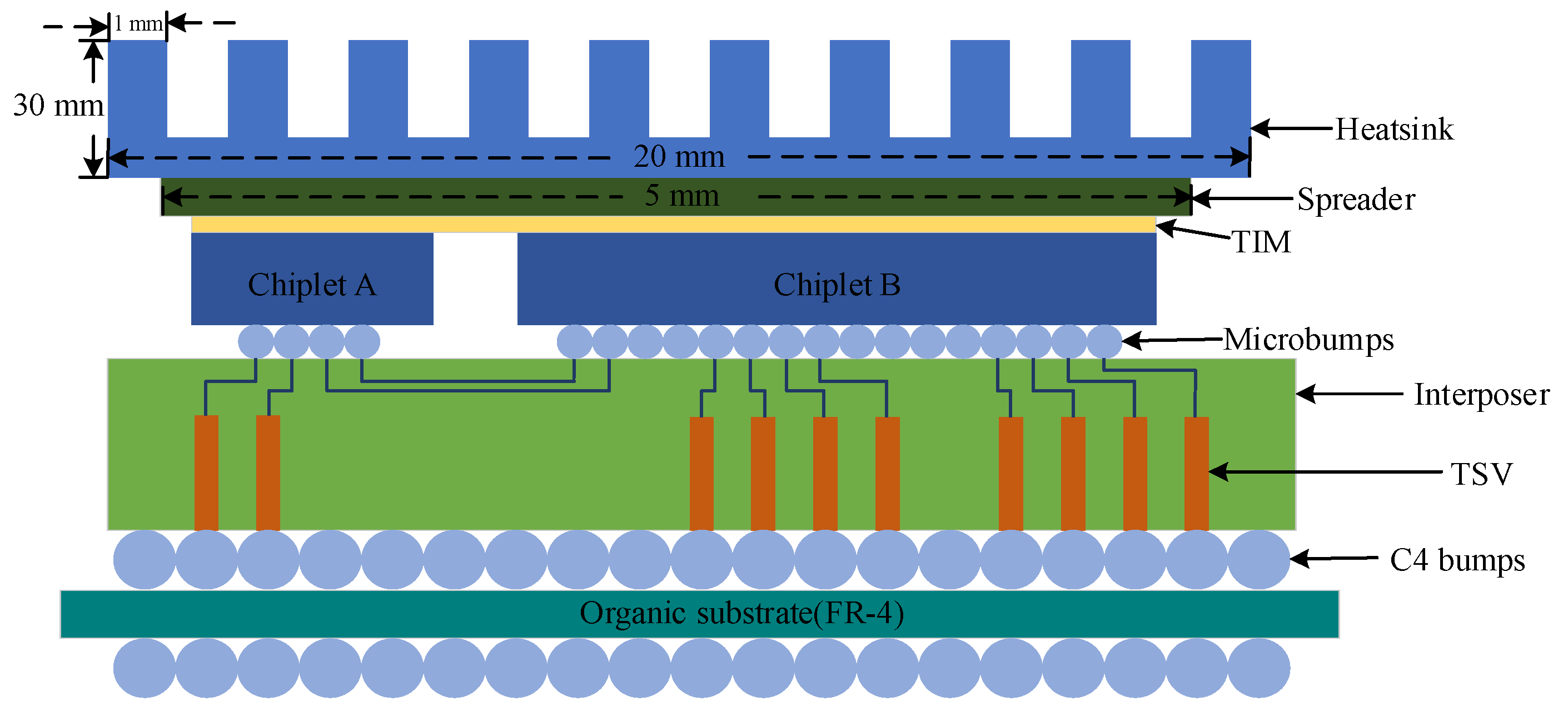
In Figure 1, passive interposer with six layers is used as an example in this paper. From bottom to up, the layers are organic substrate, a controlled collapse chip connection layer (C4 bump layer), silicon interposer, microbump layer, chiplet layout, and thermal interface material (TIM). The spreader and heatsink are also taken into account in our model to simulate the real situation as much as possible. We defined the parameters (such as layer thickness, materials, dimensions of bumps, and through silicon vias (TSVs)) of each layer of the 2.5-D system in detail. Additionally, we use a realistic air-forced heatsink as the cooling technique.
We set these parameters in detail in Hotspot: we set the ambient temperature to 318.5 K, the heat spreader edge size to be 5 mm, and the heatsink edge size to be 20 mm. Additionally, in order to obtain better heat dissipation, we used forced convection cooling and lateral airflow from the sink side. We also selected a fin-channel heat sink as the heat sink type, and the fin-height is 30 mm and the fin-width is 1 mm. The fan radius is set to 10 cm and the fan speed is set to 5000 revolutions per minute. Unlike finite element simulation tools, Hotspot can quickly evaluate 2.5-D system temperatures and make judgments about the system reliability.
3.2. Chiplet Multi-Objective Optimization Algorithm Description
3.2.1. Topology Generation
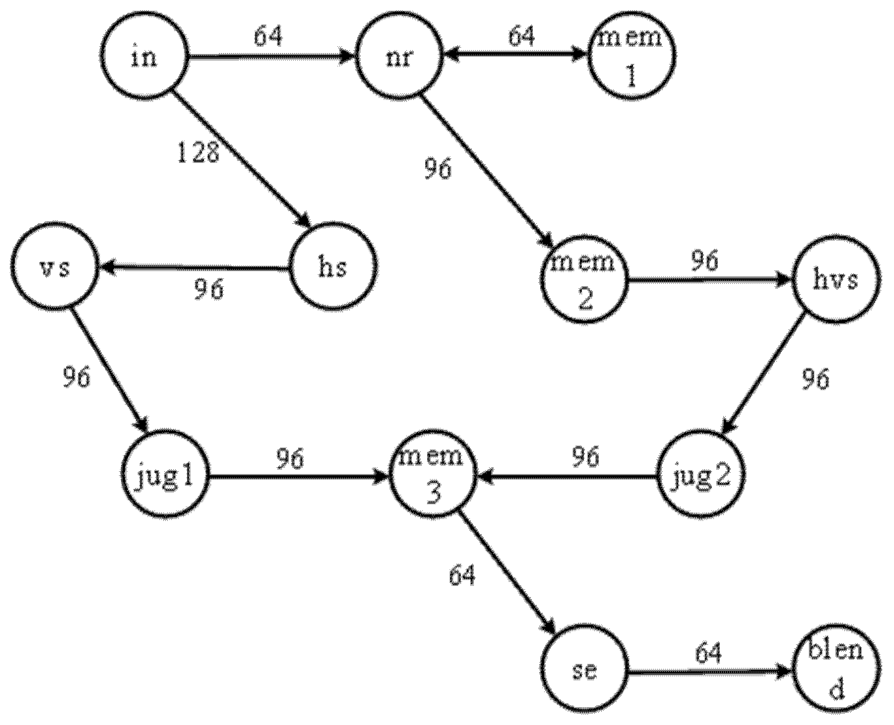
In this article, mesh topology is used. Mesh topology is a common direct type of structure, meaning that the neighboring nodes are connected in a point-to-point manner or direct interconnection. Mesh topology is the most widely used topology for NoC because it has the advantages of easy implementation and good network scalability. We use multi-window display (MWD) [28] as a concrete example to validate our algorithm. MWD is a SoC example of a multimedia application with 12 IP cores. We separate the monolithic system into 12 chiplets for 2.5-D integration. Figure 2 is the communication task between chiplets, the names in the circles represent different chiplets, and the numbers on the directed line segment represent the communication volume (Mbit/s) between chiplets and communication direction.
According to the communication task diagram, we can get the communication priority list (CPL) in Table 1, and the one with large communication volume between chiplets will be mapped first. The order of precedence will be the same for the chiplets with same communication volume.
In order to take the area factor into account in the algorithm, it is considered that a chiplet will occupy multiple nodes in the topology. In order to make the simulation closer to the real 2.5-D system situation, we define the chiplet sizes according to its function and the power as shown in Table 2. In addition, we assume that the power is evenly distributed over the chiplet, and due to the chiplet’s thinness and high thermal conductivity, we assume that the surface temperature of the chiplet is consistent with the overall temperature. [29]. The complexity of the operation will significantly rise if the chiplet shape and chiplet spacing are considered at the same time, thus the chiplet sizes are preprocessed and the theoretical sizes, which are the actual size plus the distance, are introduced. The theoretical size of the chiplets will determine the appropriate unit grid size and the number of grids that each chiplet is occupying. For instance, the size of the chiplet_blend in MWD is 2.5 mm × 2.5 mm; considering the spacing, this chiplet is defined to occupy 2 × 2 grids and its theoretical size is 4.0 mm × 4.0 mm. Similarly, the theoretical size of the remaining chiplets can be obtained, as shown in Table 2. It should be noted that the theoretical size can be easily adjusted according to the actual chiplet properties in other cases.
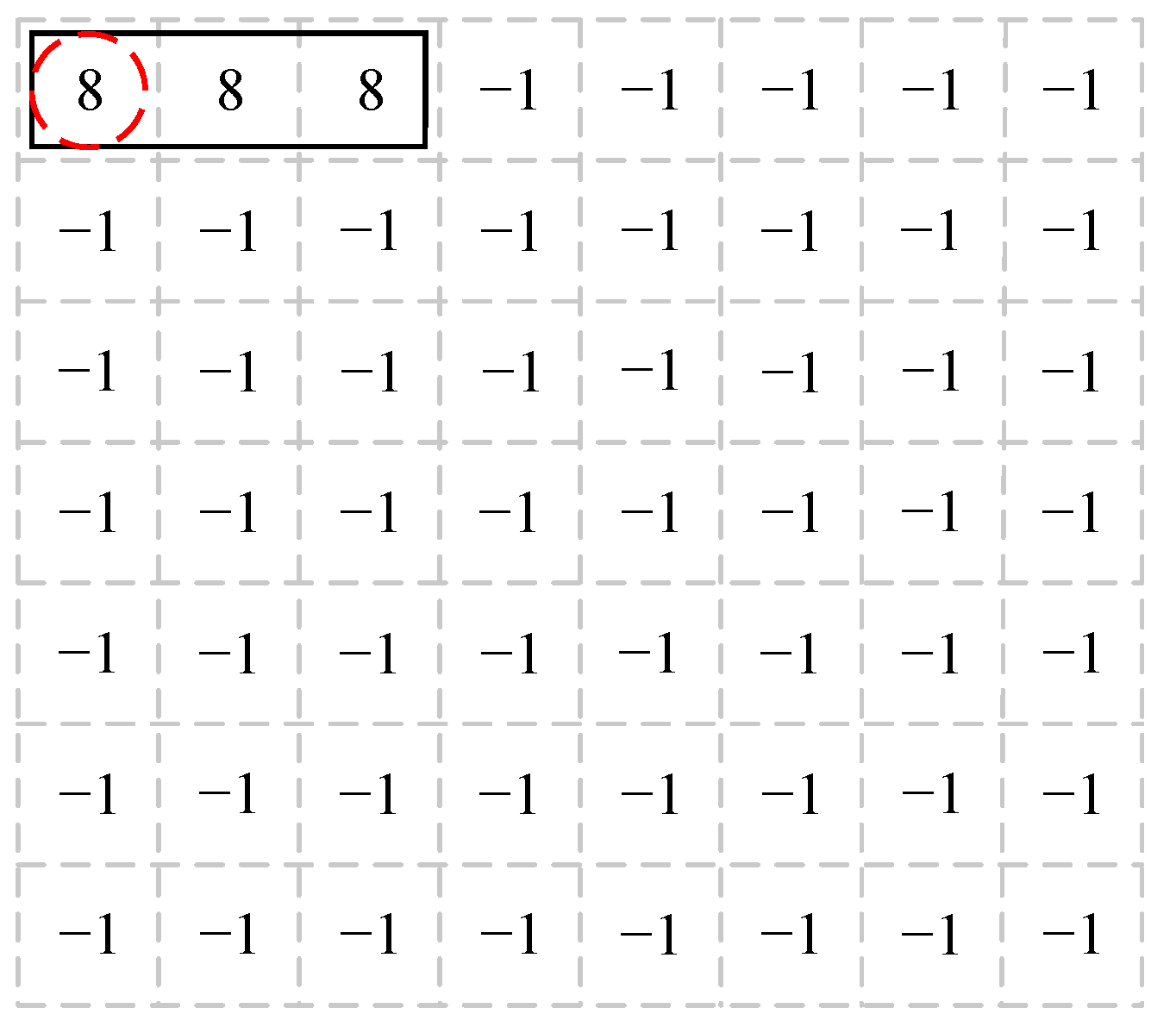
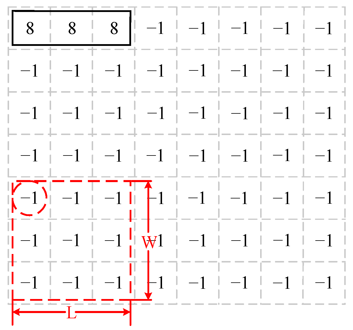
Figure 3 shows the mapping schematic diagram of chiplet_8 (mem3, the first chiplet in CPL). The number “8” in the topology indicates that the chiplet_8 is mapped in these areas, and the number “−1” indicates that these nodes are not mapped. The coordinates of the node in the upper left corner of a chiplet area are used to indicate the position, as the node circled by the dotted lines in Figure 3.
3.2.2. The Number and Location of the Initial Nodes
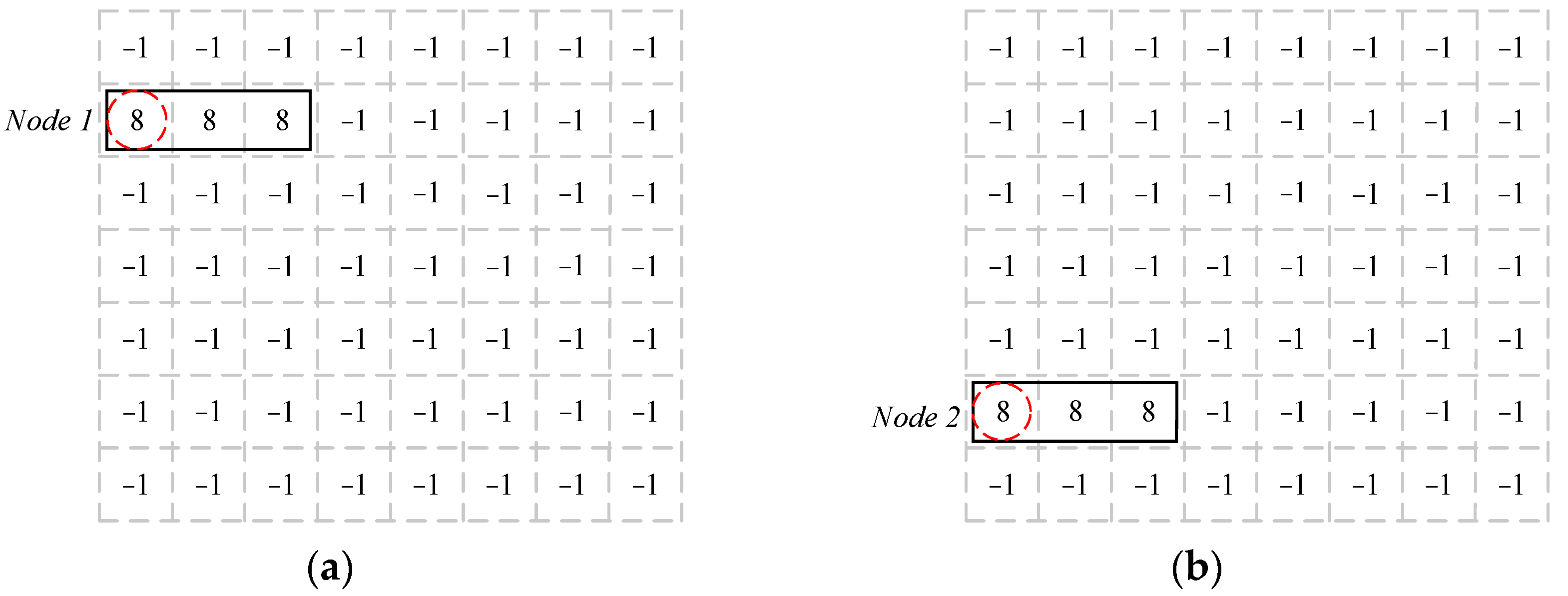
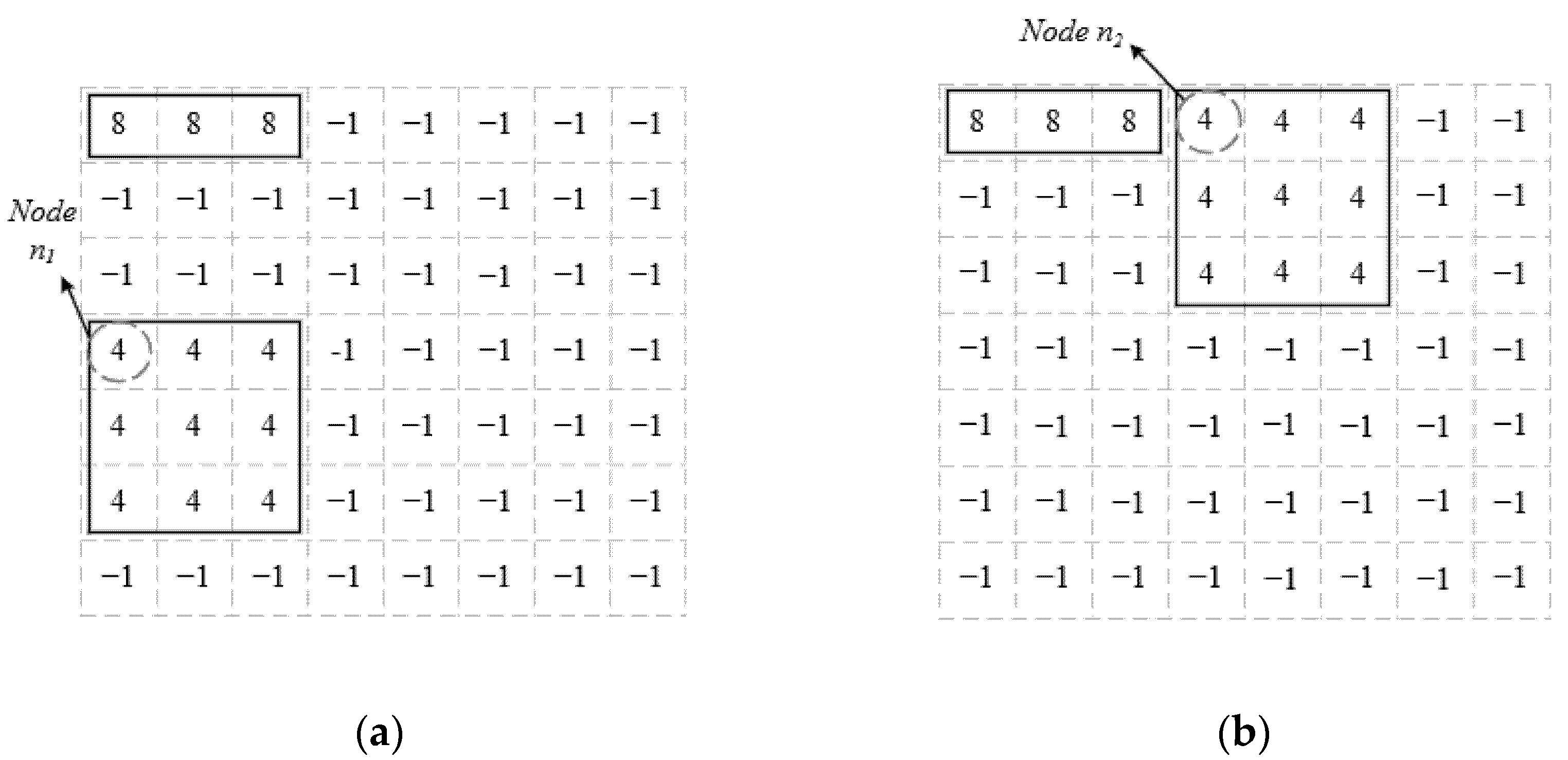
The number of mapping solutions in this algorithm will be determined by where the beginning node is located. To find an ideal layout as the outcome, we should discover every layout produced by various initial nodes. In this algorithm, grid topology is used, and some of the nodes have the same mapping effects due to symmetry of grid topology. These symmetric nodes only need to be computed once during the algorithm process. In Figure 4, the first chiplet to be mapped of this 2.5-D system is chiplet_8, and when searching the initial nodes, the node 1 and node 2 are symmetrical in the vertical direction, so the layouts generated by these two initial nodes will have the same communication consumption. Only one of them needs to be computed in the algorithm and the algorithmic procedure will be significantly simplified by this way. In addition, the quantity and the locations of initial nodes are related to the size of topology and the size of initial chiplet, as is given by Algorithm 1.
| Algorithm 1 Initial node generation |
| Input: topology length N1, width N2. chiplet length L0, width W0. |
| Output: number of schemes, M. Initial node matrix, initial_node []. |
| 1.int x = ceil ((N1 − L0 + 1)/2); |
| 2.int y = ceil ((N2 − W0 + 1)/2); |
| 3.int M = x × y; |
| 4.int k = 0; |
| 5.for (int i = 0; i < x; i++) |
| 6.{ |
| 7. for (int j = 0; j < y; j++) |
| 8. { |
| 9. initial_node[k] = i + j × N1; |
| 10. k++; |
| 11. } |
| 12.} |
3.2.3. Selecting Mapping Area
After determining the location of the initial node and mapping the initial chiplet, it is necessary to decide where to map the next chiplet. In the mapping process, there may be cases where the unmapped area is smaller than the size of chiplet, and these areas will not be able to map the current chiplet, so the unmapped areas need to be filtered. In Figure 5, if the length of the chiplet currently mapped is L and the width is W, and if there exists a rectangular area of nodes with width W and length L that both have the value “−1” (not mapped), the coordinates of this node (the upper left corner of the region) will be chosen and recorded. The final mapping node will be selected from these alternative nodes. The specific judgment method is given by Algorithm 2.
| Algorithm 2 Next chiplet selection |
| Input: topology length N1, width N2 chiplet length L, width W. mapping flag matrix, mflag []. counting matrix, count []. |
| Output: selection flag matrix, sflag []. |
| 1.for (int k = 0; k < L × W; k++) |
| 2. { |
| 3. for (int w = 0; w < W; w++) |
| 4. { |
| 5. for (int l = 0; l < L; l++) |
| 6. { |
| 7. if (mflag [k + l + w × N1]) == −1 && |
| 8. L1 <= (N1 − k % N1) && W <= N2 − floor (k/N1)) |
| 9. count[k]++; |
| 10. } |
| 11. } |
| 12. } |
| 13.for (int k = 0; k < L × W; k++) |
| 14. { |
| 15. if (count[k] == L1 × W1) |
| 16. { |
| 17. sflag[k1] = 1; |
| 18. } |
| 19. } |
3.2.4. Computing Heuristic Information and Mapping Chiplets
The heuristic information represents the probability of this node being selected. When the potential mapping area is determined, the heuristic information of these nodes should be calculated to select an appropriate node to map this chiplet. This algorithm is optimized for both chiplet communication consumption and temperature, so the communication-based heuristic information and the temperature-based heuristic information are proposed in this article.
The communication-based heuristic information is proportional to the spacing of chiplets and the communication data; that is, the wider the distance and the greater the communication consumption between chiplets, the greater the communication-based heuristic information, as indicated by Equation (1). The temperature-based heuristic information is proportional to the power and inversely proportional to the spacing; that is, the higher the power of the chiplet, the greater its influence on the temperature of other chiplets, and the greater the distance between chiplets, the smaller its influence on the temperature of the other chiplets. The calculation method is shown in Equation (2).
where i represents the chiplet_i, which is to be mapped, j represents the chiplet_j that was already mapped. Furthermore, di,j is the Manhattan distance between chiplet_i and chiplet_j. Ci,j is the communication consumption between chiplet_i and chiplet_j, and Ebit is the energy consumed to transmit 1 Mb data per unit distance between chiplets [30]. Pj is the power of chiplet_j.
This optimization algorithm computes temperature-based and communication-based heuristic information. To demonstrate how the algorithm’s emphasis on temperature and communication consumption differs, the weight α (0 ≤ α ≤ 1) of communication and temperature heuristic information is used in our algorithm. If the desired algorithm result is more focused on minimizing communication power consumption, α should take a larger value; correspondingly, if the desired algorithm result is more focused on minimizing temperature, α will take a smaller value. The designer can adjust α according to different requirements, and α = 0.5 is taken for calculation in this example. The communication consumption and temperature-based heuristic information are also normalized using min–max scaling to alleviate the impact of imbalanced values and ranges of raw data according to Equation (3).
where is the communication heuristic of chiplet_i, and , are its minimum and maximum. is the temperature heuristic of chiplet_i, and , are its minimum and maximum. The details of the calculation are given by Algorithm 3.
| Algorithm 3 Heuristic information caculation |
| Input: chiplet number NR; mapping flag matrix mapflag[]; distance matrix D[][]; mapping matrix map[]; the number of node being mapped k; weighing factor α;maximum and minimum heuristic factors, , , , ; output: optimal node node; |
| 1.for(int i = 0; i < NR; i++) |
| 2.{ |
| 3. for(int j = i + 1; j < NR; j++) |
| 4. { |
| 5. if(mapflag[i]== −2&&mapflag[j]== −2) |
| 6. comcost+=D[i][j] × cost[i][j] × 0.186; |
| 7. } |
| 8.} |
| 9. for( int i = 0; i < NR; i++) |
| 10.{ |
| 11. if( i ! = k&&map[i]== −2) |
| 12. { |
| 13. temcost+=power[mapp[i]]/D[map[i]]D[map[k]]; |
| 14. } |
| 15.} |
| 16. cost = α* (comcost − )/( − ) + (1 − α) × (temcost − )/ |
| 17. ( − ); |
| 18.if(cost < cost_min) |
| 19.{ |
| 20. cost_min = cost; |
| 21. node = i; |
| 22.} |
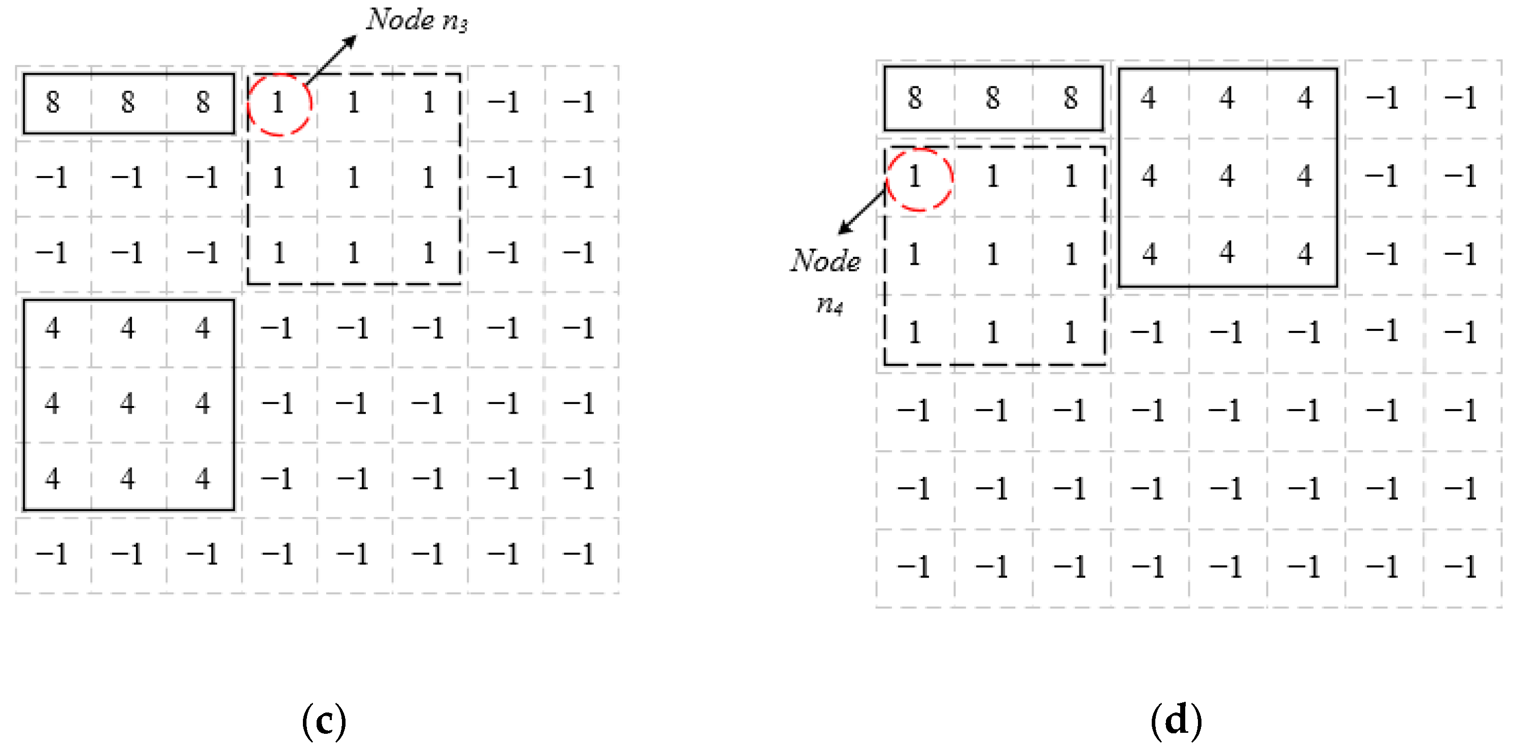
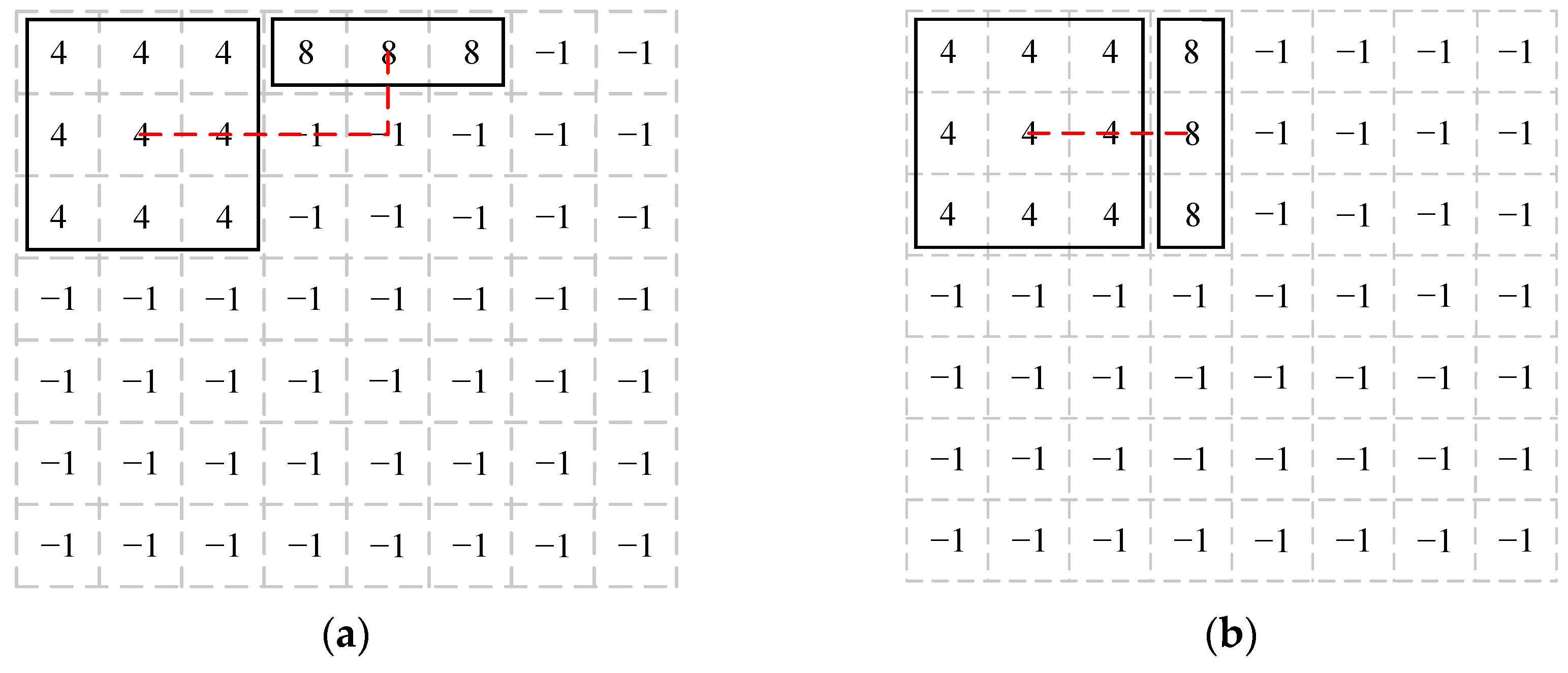
There also exist nodes that make the heuristic information equal in the filtering process, and the secondary exploration method will be applied. This approach will map chiplets based on the assumption that the current chiplet was mapped to one of the nodes having the same heuristic information, and the minimum heuristic information in this scenario is computed. Compare the heuristic information of these nodes, and the minimum of them will be selected as the mapping node. Figure 6 shows an example, chiplet_4 is the chiplet to be mapped, and when chiplet_4 is mapped to node n1 (Figure 6a) and node n2 (Figure 6b), the heuristic information and are equal. Suppose chip_4 employs the mapping scheme depicted in Figure 6a and in this case chiplet_1 (the next chiplet to be mapped) is mapped in the remaining nodes. In Figure 6c, calculate the minimum of the heuristic information in the remaining nodes when mapping chiplet_1, and record the heuristic information and the node n3. Similarly, in Figure 6d, calculate the minimum of the heuristic information in the remaining nodes, and record the heuristic information and node n4. If is greater than , node n3 will be selected to map chiplet_4; on the contrary, n2 will be selected.
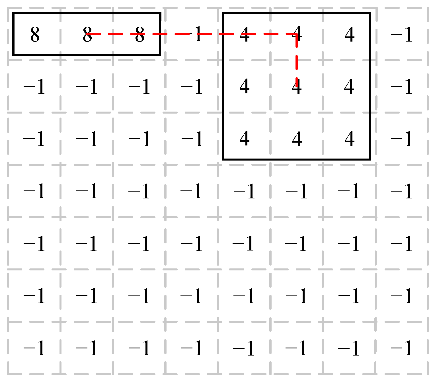
The chiplet distance is also involved in the calculation of the heuristic information. A single chiplet will occupy multiple nodes in grid topology, and the Manhattan distance between the midpoints is taken as the average distance, as the dashed line shows in Figure 7.
When the distance between chiplets is calculated in this way, the distance of vertical and horizontal placement will also be different if the chiplet is not square. In Figure 8, the distance between chiplet_8 and chiplet_4 is four grids when chiplet_8 is placed horizontally, and when chiplet_8 is placed vertically, the distance between chiplets is two grids. Therefore, when selecting the mapping nodes, the heuristic information should be calculated separately for the horizontal and vertical placement, and the placing methods with minimum heuristic information will be taken as the mapping result.
One chiplet can be mapped using the aforementioned steps, and the remaining chiplets will be mapped by repeating this method. The different layouts derived from the algorithm will be compared, and the layout with lower communication consumption and better temperature distribution will be selected as the final mapping scheme.
4. Evaluation Results
The algorithm uses C++ language to verify its validity and accuracy. To test the algorithm results, Hotspot tools are used to obtain the temperature distribution for different layouts. The Hotspot tools perform temperature analysis by calculating the thermal resistance matrix between chips, which allows predictive analysis of the system and gets results relatively fast.
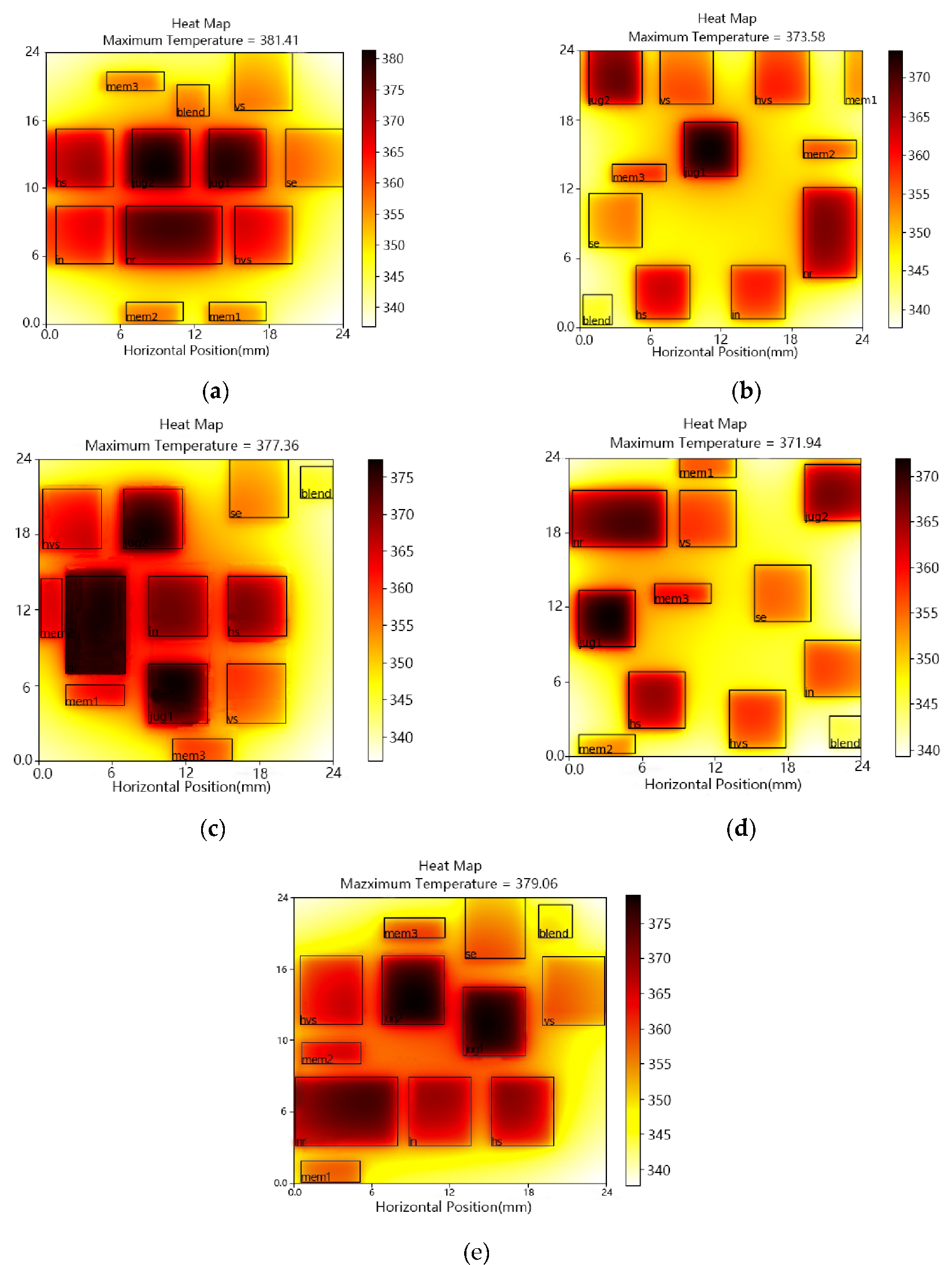
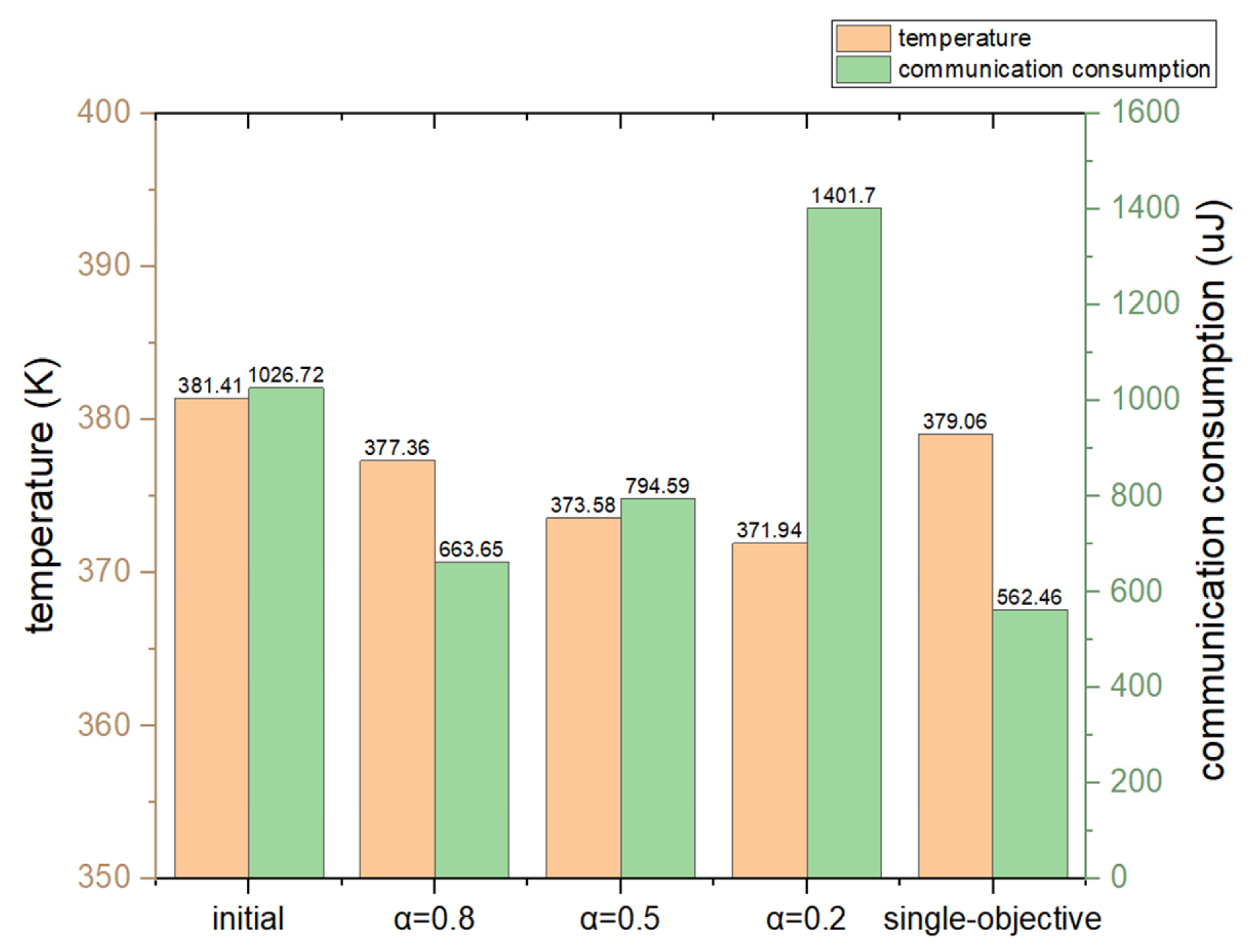
Figure 9a shows the thermal map of the initial layout. The temperature is 381.41 K, and the communication consumption between chiplets is 1026.72 uJ. Figure 9b shows the temperature map of the layout generated by the CMO algorithm with α equal to 0.5, which optimized the temperature and the communication consumption at the same time. The maximum temperature drops to 373.58 K, while the communication usage drops to 794.59 uJ. Through the algorithm, maximum temperature and communication consumption were clearly optimized compared to the initial layout, with peak temperature reduced by 8.34 K and communication power consumption reduced by 232.13 uJ. Furthermore, we get a temperature map of the layout with α equal to 0.8, as shown in Figure 9c. This layout is more focused on optimizing the communication consumption compared to Figure 9b, but it will have a relatively higher peak temperature. The peak temperature is 377.36 K and communication consumption is 663.65 uJ. Figure 9d shows the result with α equal to 0.2. The temperature is 371.94 K, and the communication consumption between chiplets is 1401.70 uJ. This layout is more focused on optimizing the system temperature, but communication consumption will be relatively higher. Figure 9e is the temperature map of the single-objective optimization [31] result, which optimizes the communication consumption only. The communication consumption was even less compared to the multi-objective optimization result (α = 0.5). However, the maximum temperature is not significantly optimized. Figure 10 shows the comparisons of temperatures and communication consumption for different layouts.
5. Conclusions
In this article, we propose a multi-objective optimization algorithm, which optimizes the communication consumption and the system temperature at the same time. Communication and temperature-based heuristic information is introduced to make a balance between them by using the weight factor α. Through the algorithm, maximum temperature and communication consumption (α = 0.5) were clearly optimized compared to the initial layout, with the peak temperature reduced by 8.34 K and communication power consumption reduced by 232.13 uJ. Additionally, the communication consumption of the layout with the α equal to 0.8 is 663.65, and the temperature is 377.36 K. This layout focuses more on optimizing the communication consumption compared to the layout with the α equal to 0.5. Similarly, the communication consumption of the layout with the α equal to 0.2 is 1401.70 uJ, and the temperature is 371.94 K, which focuses more on optimizing the temperature. The factor α can effectively adjust the weight of communication power consumption and temperature in the algorithm. Designers can change the weight factor according to their requirements.
Author Contributions
Conceptualization, H.S. and Y.L.; methodology, H.S. and X.P.; software, H.S., X.P. and D.C.; validation, X.P.; formal analysis, X.P.; investigation, X.P. and D.C.; data curation, X.P.; writing—original draft preparation, X.P.; writing—review and editing, H.S. and X.P.; visualization, D.C.; supervision, H.S., J.Z. and J.F. All authors have read and agreed to the published version of the manuscript.
Funding
This research was funded by the National Natural Science Foundation of China 61974077.
Data Availability Statement
The data reported in this study are included in the article.
Conflicts of Interest
The authors declare no conflict of interest.
References
- Moore, G.E. Cramming more components onto integrated circuits. Proc. IEEE 1998, 86, 82–85. [Google Scholar] [CrossRef]
- Kabir, M.D.A.; Peng, Y. Holistic Chiplet—Package Co-Optimization for Agile Custom 2.5-D Design. IEEE Trans. Compon. Packag. Manuf. Technol. 2021, 11, 715–726. [Google Scholar] [CrossRef]
- Lim, S.P.S.; Chidambaram, V.; Jaafar, N.; Seit, W. Development of 2.5 D high density device on large ultra-thin active interpose. In Proceedings of the 2019 IEEE 21st Electronics Packaging Technology Conference (EPTC), Singapore, 4–6 December 2019; pp. 247–252. [Google Scholar]
- Chaware, R.; Nagarajan, K.; Ramalingam, S. Assembly and reliability challenges in 3D integration of 28nm FPGA die on a large high density 65nm passive interposer. In Proceedings of the 2012 IEEE 62nd Electronic Components and Technology Conference, San Diego, CA, USA, 29 May–1 June 2012; pp. 279–283. [Google Scholar]
- Coskun, A.; Eris, F.; Joshi, A.; Kahng, A.B.; Ma, Y.; Narayan, A.; Srinivas, V. Cross-layer co-optimization of network design and chiplet placement in 2.5-D systems. IEEE Trans. Comput.-Aided Des. Integr. Circuits Syst. 2020, 39, 5183–5196. [Google Scholar] [CrossRef]
- Vivet, P.; Guthmuller, E.; Thonnart, Y.; Pillonnet, G.; Fuguet, C.; Miro-Panades, I.; Moritz, G.; Durupt, J.; Bernard, C.; Varreau, D.; et al. IntAct: A 96-core processor with six chiplets 3D-stacked on an active interposer with distributed interconnects and integrated power management. IEEE J. Solid-State Circuits 2020, 56, 79–97. [Google Scholar] [CrossRef]
- Kim, J.; Chekuri, V.C.K.; Rahman, N.M.; Dolatsara, M.A.; Torun, H.; Swaminathan, M.; Mukhopadhyay, S.; Lim, S.K. Silicon vs. Organic Interposer: PPA and Reliability Tradeoffs in Heterogeneous 2.5 D Chiplet Integration. In Proceedings of the 2020 IEEE 38th International Conference on Computer Design (ICCD), Hartford, CT, USA, 18–21 October 2020; pp. 80–87. [Google Scholar]
- Li, T.; Hou, J.; Yan, J.; Liu, R.; Yang, H.; Sun, Z. Chiplet heterogeneous integration technology—Status and challenges. Electronics 2020, 9, 670. [Google Scholar] [CrossRef] [Green Version]
- Gupta, P.; Iyer, S.S. Goodbye, motherboard. Bare chiplets bonded to silicon will make computers smaller and more powerful: Hello, silicon-interconnect fabric. IEEE Spectr. 2019, 56, 28–33. [Google Scholar] [CrossRef]
- Coudrain, P.; Charbonnier, J.; Garnier, A.; Vivet, P.; Vélard, R.; Vinci, A.; Ponthenier, F.; Farcy, A.; Segaud, R.; Chausse, P.; et al. Active interposer technology for chiplet-based advanced 3D system architectures. In Proceedings of the 2019 IEEE 69th Electronic Components and Technology Conference (ECTC), Las Vegas, NV, USA, 28–31 May 2019; pp. 569–578. [Google Scholar]
- Datta, S.; Dutta, S.; Grisafe, B.; Smith, J.; Srinivasa, S.; Ye, H. Back-end-of-line compatible transistors for monolithic 3-D integration. IEEE Micro 2019, 39, 8–15. [Google Scholar] [CrossRef]
- Chen, T.C.; Chang, Y.W. Modern floorplanning based on B/sup*/-tree and fast simulated annealing. IEEE Trans. Comput.-Aided Des. Integr. Circuits Syst. 2006, 25, 637–650. [Google Scholar] [CrossRef]
- Coskun, A.K.; Atienza, D.; Rosing, T.S.; Brunschwiler, T.; Michel, B. Energy-efficient variable-flow liquid cooling in 3D stacked architectures. In Proceedings of the 2010 Design, Automation & Test in Europe Conference & Exhibition (DATE 2010), Dresden, Germany, 8–12 March 2010; pp. 111–116. [Google Scholar]
- Eris, F.; Joshi, A.; Kahng, A.B.; Ma, Y.; Mojumder, S.; Zhang, T. Leveraging thermally-aware chiplet organization in 2.5 D systems to reclaim dark silicon. In Proceedings of the 2018 Design, Automation & Test in Europe Conference & Exhibition (DATE), Dresden, Germany, 19–23 March 2018; pp. 1441–1446. [Google Scholar]
- Ebrahimi, M.; Weldezion, A.Y.; Daneshtalab, M. NoD: Network-on-Die as a standalone NoC for heterogeneous many-core systems in 2.5 D ICs. In Proceedings of the 2017 19th International Symposium on Computer Architecture and Digital Systems (CADS), Kish Island, Iran, 21–22 December 2017; pp. 1–6. [Google Scholar]
- Kim, J.; Murali, G.; Park, H.; Qin, E.; Kwon, H.; Chaitanya, V.; Chekuri, K.; Dasari, N.; Singh, A.; Lee, M.; et al. Architecture, chip, and package co-design flow for 2.5 D IC design enabling heterogeneous IP reuse. In Proceedings of the 56th Annual Design Automation Conference 2019, Las Vegas, NV, USA, 2–6 June 2019; pp. 1–6. [Google Scholar]
- Kabir, M.A.; Peng, Y. Chiplet-package co-design for 2.5 D systems using standard ASIC CAD tools. In Proceedings of the 2020 25th Asia and South Pacific Design Automation Conference (ASP-DAC), Beijing, China, 13–16 January 2020; pp. 351–356. [Google Scholar]
- Yin, J.; Lin, Z.; Kayiran, O.; Poremba, M.; Altaf, M.S.B.; Jerger, N.E.; Loh, G.H. Modular routing design for chiplet-based systems. In Proceedings of the 2018 ACM/IEEE 45th Annual International Symposium on Computer Architecture (ISCA), Los Angeles, CA, USA, 2–6 June 2018; pp. 726–738. [Google Scholar]
- Park, H.; Kim, J.; Chekuri, V.C.K.; Dolatsara, M.A.; Nabeel, M.; Bojesomo, A.; Patnaik, S.; Sinanoglu, O.; Swaminathan, M.; Mukhopadhyay, S.; et al. Design flow for active interposer-based 2.5-D ICs and study of RISC-V architecture with secure NoC. IEEE Trans. Compon. Packag. Manuf. Technol. 2020, 10, 2047–2060. [Google Scholar] [CrossRef]
- Liu, Y.; Ruan, Y.; Lai, Z.; Jing, W. Energy and thermal aware mapping for mesh-based NoC architectures using multi-objective ant colony algorithm. In Proceedings of the 2011 3rd International Conference on Computer Research and Development, Shanghai, China, 11–13 March 2011; pp. 407–411. [Google Scholar]
- Ma, Y.; Delshadtehrani, L.; Demirkiran, C.; Abellan, J.L.; Joshi, A. TAP-2.5 D: A thermally-aware chiplet placement methodology for 2.5 D systems. In Proceedings of the 2021 Design, Automation & Test in Europe Conference & Exhibition (DATE), Grenoble, France, 1–5 February 2021; pp. 1246–1251. [Google Scholar]
- Healy, M.; Vittes, M.; Ekpanyapong, M.; Ballapuram, C.S.; Lim, S.K.; Lee, H.H.S.; Loh, G.H. Multiobjective microarchitectural floorplanning for 2-D and 3-D ICs. IEEE Trans. Comput.-Aided Des. Integr. Circuits Syst. 2006, 26, 38–52. [Google Scholar] [CrossRef]
- Liu, Y.; Ruan, Y.; Lai, Z. New heuristic algorithms for low-energy mapping and routing in 3D NoC. Int. J. Comput. Appl. Technol. 2013, 47, 1–13. [Google Scholar] [CrossRef]
- Skadron, K.; Stan, M.; Barcella, M.; Dwarka, A.; Huang, W.; Li, Y.; Ma, Y.; Naidu, A.; Parikh, D.; Re, P.; et al. HotSpot: Techniques for modeling thermal effects at the processor-architecture level. In Proceedings of the 8th THERMINIC Workshop, Madrid, Spain, 1–4 October 2002. [Google Scholar]
- Huang, W.; Stan, M.R.; Skadron, K.; Sankaranarayanan, K.; Ghosh, S.; Velusam, S. Compact thermal modeling for temperature-aware design. In Proceedings of the 41st Annual Design Automation Conference, San Diego, CA, USA, 7–11 June 2004; pp. 878–883. [Google Scholar]
- Stan, M.R.; Skadron, K.; Barcella, M.; Huang, W.; Sankaranarayanan, K.; Velusamy, S. Hotspot: A dynamic compact thermal model at the processor-architecture level. Microelectron. J. 2003, 34, 1153–1165. [Google Scholar] [CrossRef]
- Skadron, K.; Stan, M.R.; Sankaranarayanan, K.; Huang, W.; Velusamy, S.; Tarjan, D. Temperature-aware microarchitecture: Modeling and implementation. ACM Trans. Archit. Code Optim. 2004, 1, 94–125. [Google Scholar]
- Jaspers, E.G.; De With, P.H.N. Chip-set for video display of multimedia information. IEEE Trans. Consum. Electron. 1999, 45, 706–715. [Google Scholar] [CrossRef] [Green Version]
- Huang, W.; Ghosh, S.; Velusamy, S.; Sankaranarayanan, K.; Skadron, K.; Stan, M.R. HotSpot: A compact thermal modeling methodology for early-stage VLSI design. IEEE Trans. Very Large Scale Integr. Syst. 2006, 14, 501–513. [Google Scholar] [CrossRef]
- Kahng, A.B.; Li, B.; Peh, L.S.; Samadi, K. ORION 2.0: A fast and accurate NoC power and area model for early-stage design space exploration. In Proceedings of the 2009 Design, Automation & Test in Europe Conference & Exhibition, Nice, France, 20–24 April 2009; pp. 423–428. [Google Scholar]
- Sun, H.; Peng, X.; Cang, D.; Zhao, J.; Liu, Y. New Heuristic Algorithm for Low Energy Mapping for 2.5-D Integration. Electronics 2022, 11, 1817. [Google Scholar] [CrossRef]
Figure 1.
Schematic of 2.5-D system with passive interposer.

Figure 2.
Communication task of multi-window display chiplets.

Figure 3.
The grid topology and representation of chiplet location.

Figure 4.
(a) An example of initial chiplet placement; (b) symmetrical placement with the same mapping effect.
Figure 4.
(a) An example of initial chiplet placement; (b) symmetrical placement with the same mapping effect.

Figure 5.
Schematic diagram of the next node filtering.

Figure 6.
(a,b) An example of nodes having the same heuristic information. (c,d) Secondary exploration method to map the next chiplet.
Figure 6.
(a,b) An example of nodes having the same heuristic information. (c,d) Secondary exploration method to map the next chiplet.


Figure 7.
Chiplet spacing calculation method.

Figure 8.
Different distance of (a) vertical and (b) horizontal placement.

Figure 9.
(a) Initial layout of MWD; (b) multi-objective optimization result with α equal to 0.5; (c) multi-objective optimization result with α equal to 0.8; (d) multi-objective optimization result with α equal to 0.2; and (e) communication consumption single-objective optimization result.
Figure 9.
(a) Initial layout of MWD; (b) multi-objective optimization result with α equal to 0.5; (c) multi-objective optimization result with α equal to 0.8; (d) multi-objective optimization result with α equal to 0.2; and (e) communication consumption single-objective optimization result.

Figure 10.
Temperature and communication consumption of different layouts.


Table 1.
Communication priority list of the multi-window display system.
| Priority | Chiplet Number | Chiplet Name | Communication Data (Mbit/s) |
|---|---|---|---|
| 1 | 8 | mem3 | 256 |
| 2 | 4 | hs | 224 |
| 1 | nr | 224 | |
| 3 | 0 | in | 192 |
| 3 | vs | 192 | |
| 5 | mem2 | 192 | |
| 6 | hvs | 192 | |
| 7 | jug1 | 192 | |
| 9 | jug2 | 192 | |
| 4 | 10 | se | 128 |
| 2 | mem1 | 64 | |
| 5 | 11 | blend | 64 |
Table 2.
Chiplet sizes and powers of the multi-window display system.
| Chiplet Name | Chiplet Theoretical Size (mm2) | Chiplet Actual Size (mm2) | Power (W) |
|---|---|---|---|
| mem3 | 6.0 × 2.0 | 4.5 × 1.5 | 10 |
| hs | 6.0 × 6.0 | 4.5 × 4.5 | 40 |
| nr | 8.0 × 6.0 | 7.5 × 4.5 | 70 |
| in | 6.0 × 6.0 | 4.5 × 4.5 | 30 |
| vs | 6.0 × 6.0 | 4.5 × 4.5 | 20 |
| mem2 | 6.0 × 2.0 | 4.5 × 1.5 | 10 |
| hvs | 6.0 × 6.0 | 4.5 × 4.5 | 30 |
| jug1 | 6.0 × 6.0 | 4.5 × 4.5 | 50 |
| jug2 | 6.0 × 6.0 | 4.5 × 4.5 | 50 |
| se | 6.0 × 6.0 | 4.5 × 4.5 | 20 |
| mem1 | 6.0 × 2.0 | 4.5 × 1.5 | 10 |
| blend | 4.0 × 4.0 | 2.5 × 2.5 | 5 |
Disclaimer/Publisher’s Note: The statements, opinions and data contained in all publications are solely those of the individual author(s) and contributor(s) and not of MDPI and/or the editor(s). MDPI and/or the editor(s) disclaim responsibility for any injury to people or property resulting from any ideas, methods, instructions or products referred to in the content. |
© 2023 by the authors. Licensee MDPI, Basel, Switzerland. This article is an open access article distributed under the terms and conditions of the Creative Commons Attribution (CC BY) license (https://creativecommons.org/licenses/by/4.0/).
Share and Cite
MDPI and ACS Style
Sun, H.; Peng, X.; Cang, D.; Zhao, J.; Liu, Y.; Fang, J. Chiplet Multi-Objective Optimization Algorithm Based on Communication Consumption and Temperature. Electronics 2023, 12, 1604. https://doi.org/10.3390/electronics12071604
AMA Style
Sun H, Peng X, Cang D, Zhao J, Liu Y, Fang J. Chiplet Multi-Objective Optimization Algorithm Based on Communication Consumption and Temperature. Electronics. 2023; 12(7):1604. https://doi.org/10.3390/electronics12071604
Chicago/Turabian StyleSun, Haiyan, Xinwei Peng, Dongqing Cang, Jicong Zhao, Yanhua Liu, and Jiaen Fang. 2023. "Chiplet Multi-Objective Optimization Algorithm Based on Communication Consumption and Temperature" Electronics 12, no. 7: 1604. https://doi.org/10.3390/electronics12071604
Note that from the first issue of 2016, this journal uses article numbers instead of page numbers. See further details here.