1. Introduction
Due to the demand for smart electronics, complementary integrated circuits, and biological and medical applications, the next generation of electronic devices with transparency has received a great deal of attention. Transparent electronics technology has greatly expanded the application scenarios of electronic devices, and transparent electronics have a wider range of applications [
1,
2,
3]. Devices based on transparent electronics can be integrated on a variety of transparent substrates, and this convenience will greatly expand the application of electronic devices, such as applications in car windscreens, solar photovoltaic, intelligent lighting, displays, etc., where electronic devices imposed on these areas not only have to often take into account the problem of light transmission or view but also the space occupied by additional electronic devices [
4]. Transparent electronics can be used for a wide range of applications without compromising functionality or taking up extra space. The growing use of transparent electronics not only offers additional advantages in terms of application but is also very much in line with current aesthetic trends and meets people’s needs in terms of the appearance of the device. The demand for transparent electronic components is growing in order to meet a variety of applications and aesthetic requirements.
The rapid development of the Internet of Things and 5G continues to increase the amount of information that needs to be processed. Conventional computer systems based on the von Neumann architecture face major obstacles due to the limitations of separating storage and computation [
5]. Considering the bottleneck of Moore’s Law and the challenges from the von Neumann architecture, conventional semiconductor devices cannot meet the urgent need for high performance and low power consumption. In contrast, the biological neural network in the human brain has a large number of parallel configurations—10
10–10
12 neurons and 10
12–10
15 synapses inside, weighs only 1 KG, and operates at less than 20 W [
6]—all of which are better features than the traditional von Neumann architecture. Neurons and synapses in the human brain learn and remember in an integrated manner, so neuromorphic computing based on brain-like structures offers a promising route to solving these problems, and simulating biological synapses with electronic devices is an important aspect of building hardware-based artificial intelligence interconnections.
Organic artificial synapses can effectively simulate the structure and function of biological synapses and can therefore be applied to a variety of neuromorphic electronic devices, showing great promise in future neuromorphic devices [
7,
8,
9]. The artificial synapses that have been reported now can be divided into two types based on their structure: a two-terminal artificial synapse and a three-terminal artificial synapse. Among the two-terminal devices, the memristor, proposed by Prof. L. Chua, is one of the most commonly used devices for studying neuromorphic computation [
10]. Artificial synaptic devices based on a memristor structure are used to modulate synaptic plasticity by changing the conductivity between two electrodes. One electrode is regarded as the front end of the neuron, where a voltage pulse is applied to stimulate the synaptic device; the other electrode is regarded as the back end of the neuron, where the current is tested and delivered. Fu et al. reported a LiAlO
X-based synaptic memristor with resistance-switching characteristics dependent on the formation and breakage of oxygen-vacancy-type conductive filaments [
11]. The conductive channel formation of a conductive filament memristor is very similar to the opening of ion channels at biological synapses, and its conductance can be used as a weighting to model synaptic plasticity. By adjusting the initial conductance state, a high degree of linearity in long-term potentiation (LTP)/long-term depression (LTD) behaviour is simulated, which is important for neural network calculations. Unlike the conductive wire type, the phase change type relies on the resistivity difference between the different phases of the phase change material, resulting in a resistance-switching characteristic. Kuzum et al. proposed a two-terminal memristor based on the phase-change material Ge
2Sb
2Te
5, which can simulate synaptic plasticity. The physical phase state of Ge
2Sb
2Te
5 changes when a suitable bias pulse is applied to the two terminal electrodes of the device. When Ge
2Sb
2Te
5 changes from the crystalline phase to the amorphous phase, the device changes from a low-resistance state to a high-resistance state, and the process is reversible [
12]. Wang et al. proposed a flexible and transparent artificial synaptic device with good biocompatibility consisting of (Indium-Tin Oxide) ITO/(polymer (3,4-ethoxylene dioxy thiophene: Polystyrene sodium sulfonate)) PEDOT: PSS/ITO, which is capable of pattern recognition functions [
13]. Qian et al. synthesised 2D(PEA)
2Snl
4 chalcogenide material by solution method and combined it with (reduced graphene oxide) rGO/(PEDOT: PSS) composite material to prepare a high-performance flexible photosynthetic device to achieve the synaptic response to light stimulation signal; the stability and repeatability of the device were significantly improved by adding SnF
2, and the device prepared by using rGO(PEDOT: PSS) as the electrode material has better flexibility and durability [
14]. In simple terms, a memristor is a non-linear resistor with resistance memory that can be used to achieve different resistance states depending on the writing voltage.
Compared to two-terminal memristor synapses, three-terminal transistor synaptic devices have an additional gate voltage modulation, which allows our synaptic devices to perform both learning and memory functions. It also has lower energy consumption and higher scalability. Therefore, transistors are considered ideal for simulating synaptic functions. Typically, the gate of a synaptic transistor corresponds to the presynaptic front of the organism, while the channel at the interface between the active and dielectric layers corresponds to the postsynaptic membrane, and channel conductance is mainly regulated by the gate voltage. The main types of three-terminal artificial synaptic devices based on transistor structures include floating gate, ferroelectric, and electrochemical types. Floating gate transistors have an extra gate compared to conventional transistors. A floating-gate synaptic transistor prepared by the solution method was proposed by Ce Zhou Zhao et al. Oxidised MXenes and zinc–tin oxides (ZnSnO and ZTO) are used as tunnelling layers and n-channel layers for floating barriers, respectively [
15]. When a gate voltage pulse is applied, the synaptic device exhibits basic synaptic behaviour such as excitatory postsynaptic current (EPSC)/inhibitory postsynaptic current (IPSC), paired-pulse facilitation (
PPF), short-term memory (STM), and long-term memory (LTM). Ferroelectric materials have been used in the study of memory and artificial synapses because of their special polarisation effect. Among them, Choi et al. reported a ferroelectric synaptic transistor using a semiconductor single-walled carbon nanotube (SWCNT) as the channel, featuring a ferroelectric material as the insulating layer or an additional ferroelectric layer introduced on top of the existing insulating layer [
16]. The enhancement and inhibition behaviours in synaptic plasticity are simulated by stepwise modulation of the (poly (vinylidene fluoride)) PVDF polarisation state. Finally, single devices and arrays are used for pattern recognition, with single devices achieving 80% recognition accuracy and arrays achieving over 70% recognition accuracy. Electrochemical transistors are transistors with a solid or liquid electrolyte material as the dielectric layer, which can be used to regulate channel conductance due to the presence of a large number of charged particles in the dielectric layer. Li et al. prepared an ion-gated, low-power silicon nanowire synaptic transistor with dendritic functions for neuromorphic systems [
17]. By applying in-phase or inverted frequency signals to both gates, the synaptic transistor achieves a dendritic integration function with a distinct synaptic signature. Chen et al. reported an organic light-emitting transistor with a long afterglow effect to simulate synaptic plasticity, in which (indium gallium zinc oxide) IGZO as a semiconductor layer has a significant photoconductive effect [
18]. The increase in electrical conductivity of IGZO under UV light stimulation induced an increase in luminescence, thus simulating the STP and LTP behaviour of biological synapses. This study is the first to regulate the behaviour of light output synapses through the gate, which is important for the further exploration of light output artificial synapses. Burgt et al. presented an electrochemical neuro-mimetic organic transistor synaptic device fabricated on a flexible substrate [
19]. The device consists primarily of a postsynaptic electrode composed of a PEI/PEDOT: PSS film connected to a presynaptic electrode composed of PEDOT: PSS via an electrolyte. The device is capable of modulating channel characteristics at low operating voltages at the mV level, achieving >500 conductance states and exhibiting good non-volatility. However, the aforementioned triple-ended synapses also have their drawbacks in that they require the addition of additional functional layers, which take longer and more complex processes to prepare.
Therefore, in this paper, a transparent organic synaptic transistor based on a co-hybrid heterojunction is prepared by a simple solution method by combining transparent and synaptic devices. The semiconductor layer is a blend of P-type semiconductor (IDT-BT) and N-type semiconductor (PC61BM) films; the gate dielectric layer is a PMMA film. A single-walled carbon nanotube solution (SWCNT) was sprayed through a mask and used as a gate electrode. The transparency of the device was more than 75%. Typical synaptic functions, such as excitatory/inhibitory postsynaptic currents (EPSC/IPSC), and paired-pulse facilitation (PPF) can be successfully simulated. Moreover, under specific lights, the semiconductor layer will generate excitons, resulting in an increase in the number of carriers. Thus, the device’s performance can be adjusted by using suitable light intensities. This will provide new strategies for building new multifunctional integrated devices in the field of neuromorphic computing and improve the applicability of neuromorphic devices in different contexts.
2. Materials and Methods
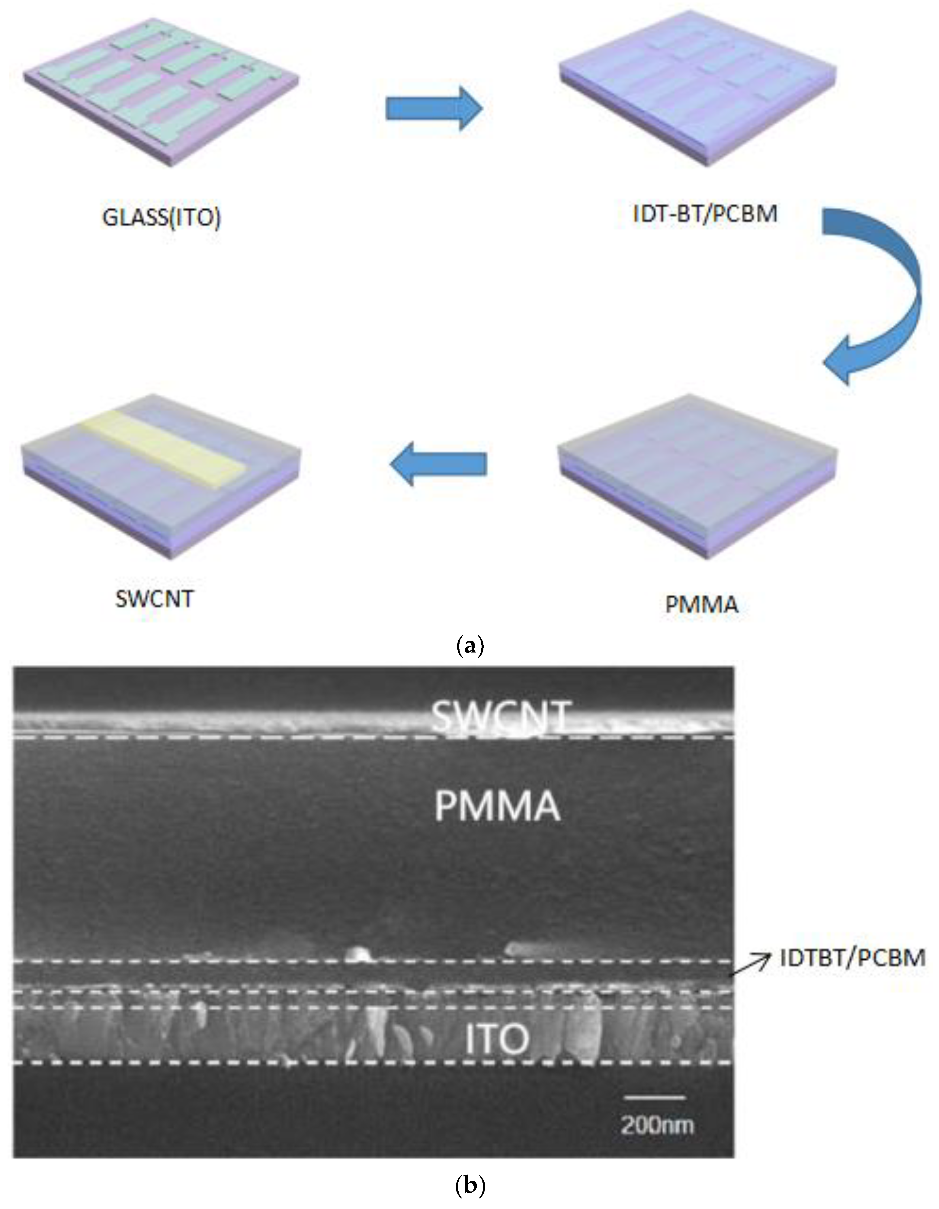
The devices are made on transparent (Indium-Tin Oxide, ITO)-coated glass; Glass is used as a substrate, while transparent source–drain electrodes are already etched on it (channel length L = 30 μm; channel width W = 30 μm).
Preparation process: The ITO was first ultrasonically cleaned in acetone, isopropanol, and ultrapure water for 10 min. It was then dried with nitrogen and placed into a plasma machine at 320 V for 30 s for plasma modification. The P-type semiconductor is enzodidithiophene benzothiadiazole (IDT-BT), and the N-type semiconductor is ([6,6]-phenyl-C61-iso methyl butyrate (PC61BM)); both were dissolved in chlorobenzene, mixed in a certain proportion (where N-type semiconductors are used as dopants, from 0% to 5%) as the semiconductor layer for the device, spin-coated onto the retouched ITO glass at 2000 rpm/60 s, and then annealed at 130 °C for 10 min. The gate dielectric layer was poly (methyl methacrylate, PMMA), and it was dissolved in toluene. The gate dielectric layer was spin-coated onto the semiconductor layer at 1300 rpm/60 s and annealed at 100 °C for 40 min. Finally, the devices were uniformly masked and sprayed with the diluted single-walled carbon nanotube solution (SWCNT), which served as the gate electrode. The process is shown in
Figure 1a. SEM of a partial cross-section of the device, as shown in
Figure 1b.
The test comprised measuring the electrical characteristics of devices using a semiconductor parameter analyser (KeyssightB2912A, Beaverton, OR, USA). The transparency was measured using an ultraviolet-visible near-infrared spectrophotometer (UV-3600 Plus, Shimadzu, Kyoto, Japan). A multimode system was used for the atomic force microscopy (AFM) scanning of surface topography.
3. Results
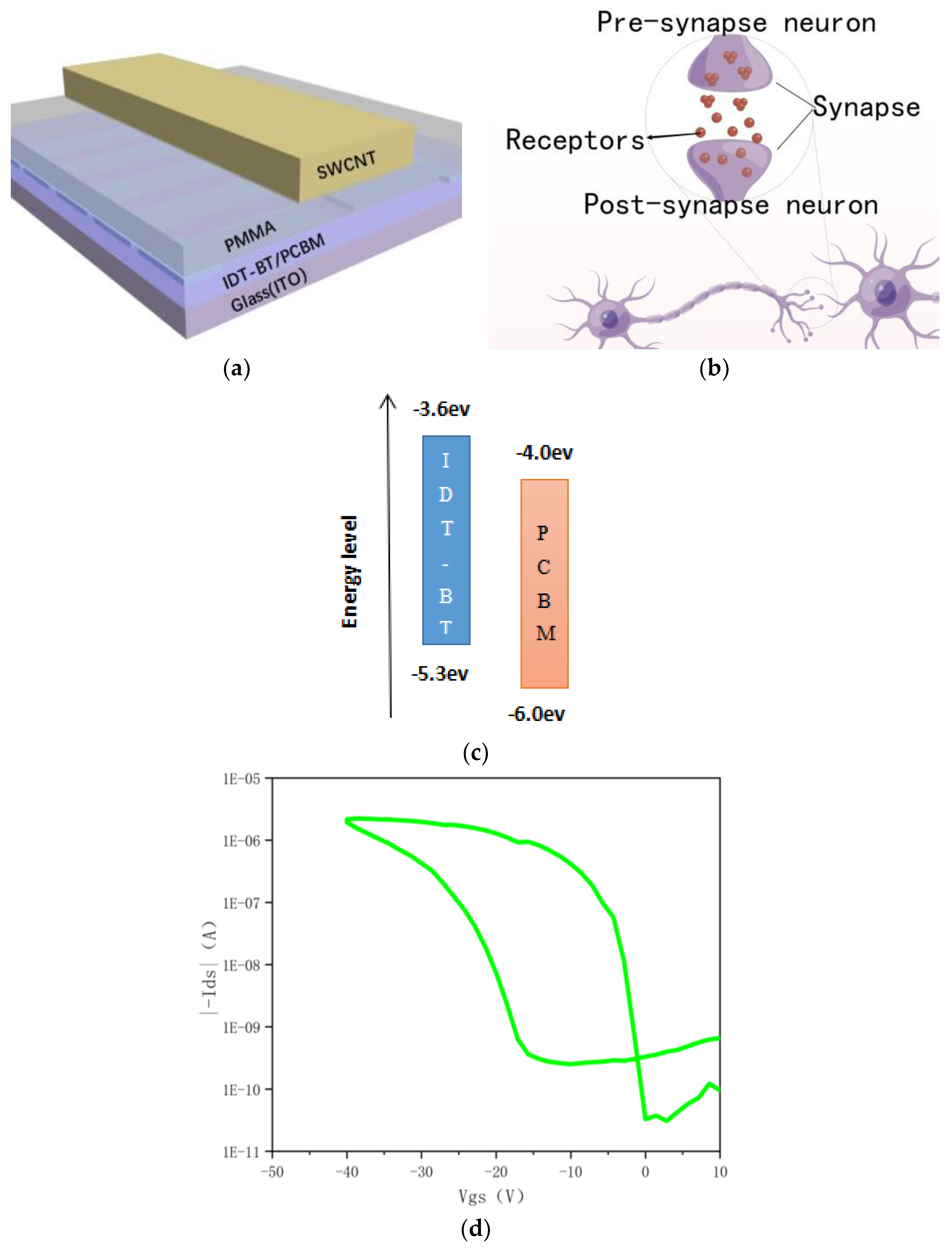
Figure 2a shows a three-dimensional schematic of a co-hybrid synaptic transistor with a top gate/bottom contact structure, where the gate electrode is used as the presynaptic terminus, and the source–drain channel is used as the postsynaptic terminus.
In a three-terminal device, the signal transmission and learning process can be performed simultaneously via the transverse conductive channel and the vertical gate channel, respectively, i.e., signal transmission and modulation can be operated simultaneously. Therefore, the essence of the artificial synapse is based on the structure of the field effect tube, using the gate electric field to overcome the energy polarity for charge transfer, thus changing the channel conductance, which is the regulation of the synaptic weight, i.e., the change in the synaptic weight relies on the input signal’s modulation.
Figure 2b shows a diagram of the biological synapse structure, with the front end of the synapse corresponding to the gate, and the back end of the synapse corresponding to the source–drain channel, where voltage stimulation on the top-gate electrode was regarded as the presynaptic terminal and the source–drain channel current served as the postsynaptic current. The semiconductor layer is an IDTBT/PCBM blend, and the devices were found to exhibit synaptic behaviour when doped with N-type semiconductors. Due to the quantum-well-like organic heterojunction, the discontinuous N-type semiconductor is set up as a charge-trapping centre, so the device does not require an additional charge-trapping functional layer, reducing device complexity and manufacturing costs.
Figure 2c shows a schematic representation of the chemical structures of IDTBT and PCBM.
Figure 2d shows the double-sweep characteristic curve of the device with 2% PCBM doping (gate voltage Vgs from 10 to −40 V, Vds = −10 V). The results show that when the doping concentration is low (2%), it reflects a good hysteresis window, which confirms the presence of charge capture in the structure. This suggests that it has potential applications in modelling synaptic function.
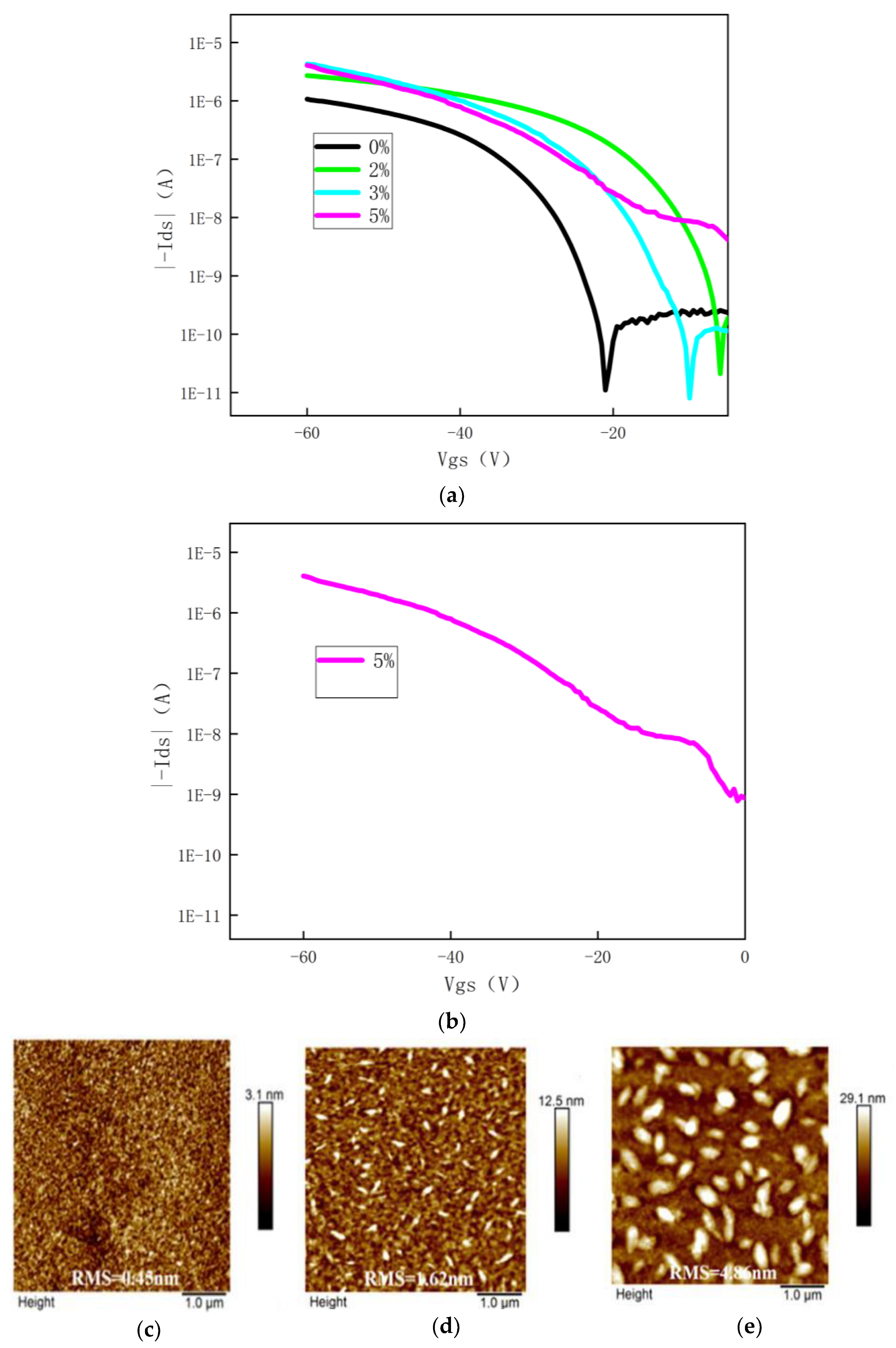
In addition, the concentration of PCBM doping as an acceptor was found to have an effect on the performance of the device. To investigate the effect of doping concentration on device performance, we recorded the variation in transfer characteristic curves for different doping concentrations of N-type semiconductors from 0% to 5% (refers to the relationship curve (Ids-Vgs) between the source–drain current and gate voltage at a fixed source–drain voltage, where the X axis is the gate voltage Vgs, and the Y axis is the source–drain current Ids corresponding to the gate voltage, where Vds = −10 V). As shown in
Figure 3a, as the doping concentration increases from 0% to 2%, a smaller effect on the switching current ratio of the device can be found in smaller amounts (2%) of the N-type polymer. The current ratio is switched to Ion/Ioff (≈10
5). However, doping concentrations from 2% to 5% have a greater effect on the device, with an increase in the off-state current, leading to a reduction in the switching current ratio, Ion/Ioff (≈10
3), as shown in
Figure 3b. Thus, the device has the best performance when the doping concentration is 2%. In order to investigate the charge-trapping density enhancement that occurs when the co-mingling concentration increases, we used atomic force microscopy (AFM) to observe the changes in film morphology when adding N-type organic semiconductors. As shown in
Figure 3c, the original IDTBT has a smooth, amorphous surface with low roughness. When doped at 2%, discrete N domains are observed in
Figure 3d. Atomic force microscopy measurements show that as the dopant concentration increases, the films show larger discrete N grain sizes and higher roughness, which creates more trapping sites for charge storage. However, with the addition of 5% N, as shown in
Figure 3e, the discontinuous N domains become continuous, disrupting the capture sites and leading to poor device performance. Therefore, subsequent studies were carried out in devices with 2% doping.
Biological synapses consist mainly of the presynaptic membrane, the postsynaptic membrane, and the synaptic gap. When the signal is transmitted across the axon and reaches the presynaptic membrane, an action potential of the appropriate size is generated, which in turn stimulates the vesicle, allowing the neurotransmitters stored in it to be released and bind to the postsynaptic membrane receptors, completing the transmission of information. The binding of protein receptors to neurotransmitters results in an excitatory postsynaptic current (EPSC) or an inhibitory postsynaptic current (IPSC) [
20].
Figure 4a,b shows the synaptic performance EPSC/IPSC of the device, which produces a current response (PSC) when a voltage pulse is applied at the gate. By applying a pulsed voltage of ±30 V for 60 ms at the gate, it was found that the postsynaptic current changes rapidly in response to the stimulation of the gate pulse voltage, followed by a rapid return to the initial value. The principle is that when a positive voltage pulse is applied to the gate electrode, electrons are trapped by the n-type semiconductor, resulting in a sudden increase in EPSC. When a negative voltage pulse is applied to the gate electrode, holes are transferred from the p-type semiconductor to the n-type semiconductor, resulting in a sudden decrease in IPSC. This is similar to biological synapses and is explained in terms of the energy band mechanism, as shown in
Figure 4c,d.
Synaptic plasticity is the neurochemical basis of learning and memory and can generally be divided into short-term plasticity (STP) and long-term plasticity (LTP). Short-term plasticity refers to the fact that when we remove the gate pulse, the postsynaptic current returns to its initial value in an extremely short period of time. In contrast, paired-pulse facilitation (
PPF), a common phenomenon in the biological nervous system, typifies the short-term plasticity of biological synapses. This is a phenomenon in which the second synaptic current is greater than the current induced by the first peak when triggered by two consecutive peaks. In biological synapses, this enhancement is usually due to an increase in the concentration of presynaptic Ca
2+, resulting in an increase in the number of neurotransmitters released by the presynaptic nerve. As a common phenomenon in biological nervous systems, it manifests itself as the short-term plasticity of biological synapses [
21]. When a biological synapse is subjected to two identical external stimuli within a short period, the latter produces a higher current in response to the stimulus than the former, and the ratio of the current in the latter to the current in the former is closely related to the time interval between stimulation. We define the
PPF index formula as follows:
where
A1 indicates the postsynaptic current amplitude generated by the first pulse voltage, and
A2 indicates the postsynaptic current amplitude generated by the second pulse voltage [
22,
23]. We apply a pulse voltage of magnitude −3 V, a duration of 30 ms, and a pulse interval of 30 ms to the gate. The postsynaptic current was found to be elevated in the latter compared to the former and slowly decayed back to its initial value when the two pulsed voltages were applied. The
PPF index decreased as the peak interval increased, and when the peak interval increased to 430 ms, the value of the
PPF index approached 100%, indicating that there was no longer a significant association between the pre- and post-stimulations. As shown in
Figure 4e, the main cause of the
PPF phenomenon is the relaxation effect of the ions during migration [
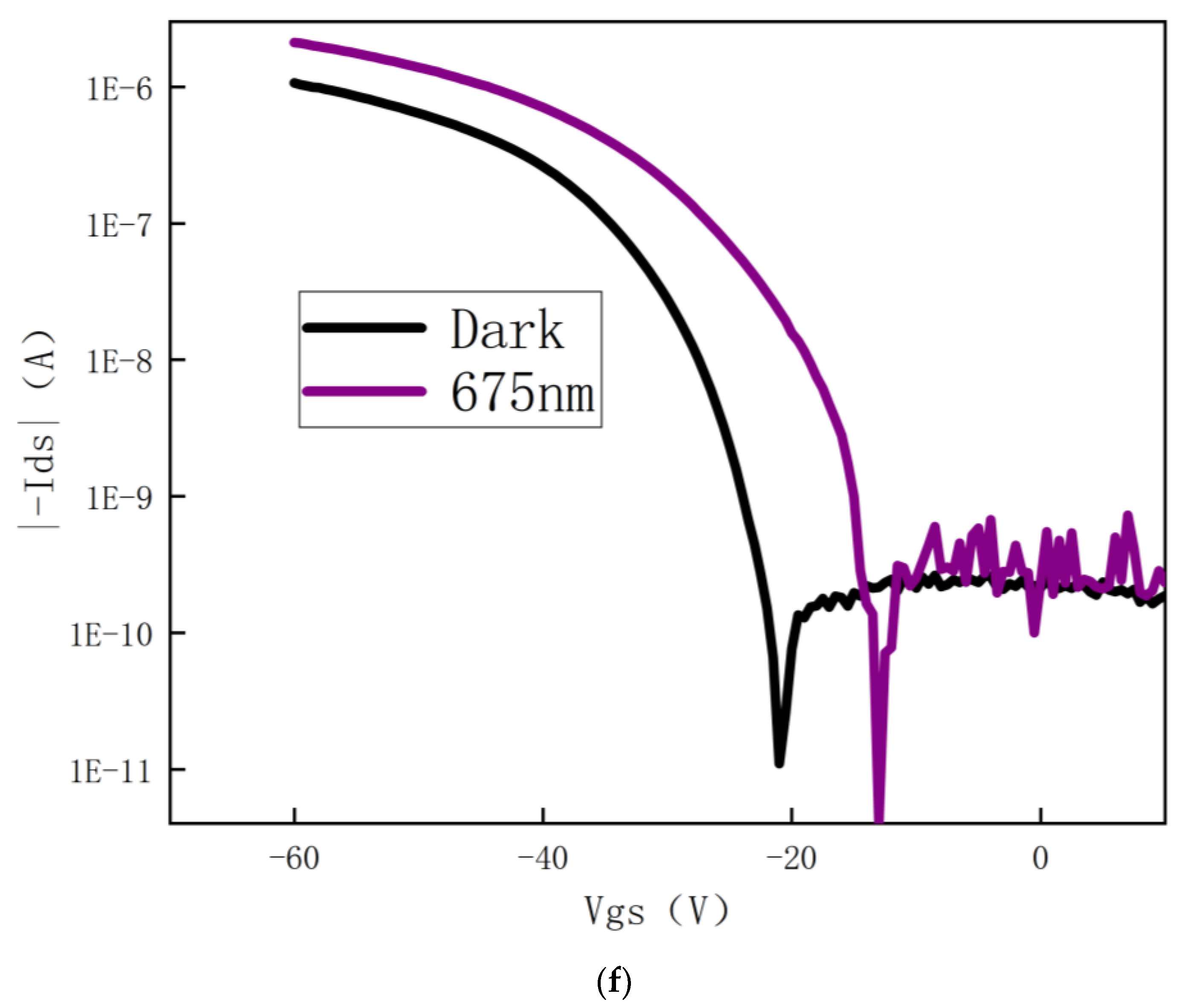
24]. In addition, it was found that when the device is irradiated in visible light (675 nm), a certain gain is produced due to the IDTBT absorbing photons and producing photo-excitation in the co-mingled film. As the LUMO level of the IDTBT is higher than that of the PCBM, the electrons will be transferred to the discrete PCBM, while the optically excited holes remain in the IDTBT, and the increase in carriers results in improved device performance. The transfer characteristic curve (Vds = −10 V) is shown in
Figure 4f.
4. Discussion
Three-terminal transistors, which are now the most compatible with the ideal object for modelling synapses, generally include floating-gate transistors, ferroelectric transistors, and electrochemical transistors.
The floating gate transistor has a large on/off ratio and controlled channel conductance but requires a high operating voltage. Ferroelectric transistors, operating in the polarised state of ferroelectric materials, also require high operating voltages. Electrochemical transistors have a low operating voltage and exhibit high switching performance, but they are unstable electrolytes. Therefore, in this paper, top-gate synaptic transistors were prepared by the solution method. The following characteristics exist.
The first characteristic is the solution method of preparation, which is convenient and fast and reduces the cost of device preparation, while the device has a transparent nature conducive to expanding its application scenarios.
The second characteristic is that no additional functional layer is required; the synaptic transistor in this study does not depend on any functional layer and is achieved simply by adding a PCBM to the IDTBT. However, the optimum ratio for N-type semiconductor doping is 2%, beyond which continuous N domains appear, disrupting the trapping mechanism and making performance poor.
Finally, the device is a top-gate-bottom contact structure with a large carrier injection area and low contact resistance, while the insulating layer on the surface has a passivating effect, which reduces the influence of water and oxygen on the semiconductor layer and increases the air stability of the device.


