Article

A High-Performance FPGA-Based Depthwise Separable Convolution Accelerator

1
The School of Electronics and Information, Hangzhou Dianzi University, Hangzhou 310018, China
2
Zhejiang Provincial Key Lab of Equipment Electronics, Hangzhou 310018, China
3
The School of Communication Engineering, Hangzhou Dianzi University, Hangzhou 310018, China
*
Authors to whom correspondence should be addressed.
Electronics 2023, 12(7), 1571; https://doi.org/10.3390/electronics12071571
Submission received: 26 February 2023 / Revised: 22 March 2023 / Accepted: 23 March 2023 / Published: 27 March 2023
(This article belongs to the Special Issue FPGA-Based Accelerators of Deep Learning and Neuromorphic Computing)

Abstract

:
Depthwise separable convolution (DSC) significantly reduces parameter and floating operations with an acceptable loss of accuracy and has been widely used in various lightweight convolutional neural network (CNN) models. In practical applications, however, DSC accelerators based on graphics processing units (GPUs) cannot fully exploit the performance of DSC and are unsuitable for mobile application scenarios. Moreover, low resource utilization due to idle engines is a common problem in DSC accelerator design. In this paper, a high-performance DSC hardware accelerator based on field-programmable gate arrays (FPGAs) is proposed. A highly reusable and scalable multiplication and accumulation engine is proposed to improve the utilization of computational resources. An efficient convolution algorithm is proposed for depthwise convolution (DWC) and pointwise convolution (PWC), respectively, to reduce the on-chip memory occupancy. Meanwhile, the proposed convolution algorithms achieve partial fusion between PWC and DWC, and improve the off-chip memory access efficiency. To maximise bandwidth utilization and reduce latency when reading feature maps, an address mapping method for off-chip accesses is proposed. The performance of the proposed accelerator is demonstrated by implementing MobileNetV2 on an Intel Arria 10 GX660 FPGA by using Verilog HDL. The experimental results show that the proposed DSC accelerator achieves a performance of 205.1 FPS, 128.8 GFLOPS, and 0.24 GOPS/DSP for input images of size 224 × 224 × 3 .

1. Introduction

Convolutional neural networks (CNNs) have been widely studied and applied to various computational vision tasks such as image classification, target detection, and autonomous driving due to their excellent performance [1,2,3]. For a long time, the mainstream line of thinking has been to improve the accuracy by increasing the network depth and complexity. However, it is difficult to implement deep networks with high computational density in embedded devices with limited computational resources, low power consumption, and high real-time characteristics. Therefore, lightweight convolutional neural network (CNN) design methods have attracted extensive research.
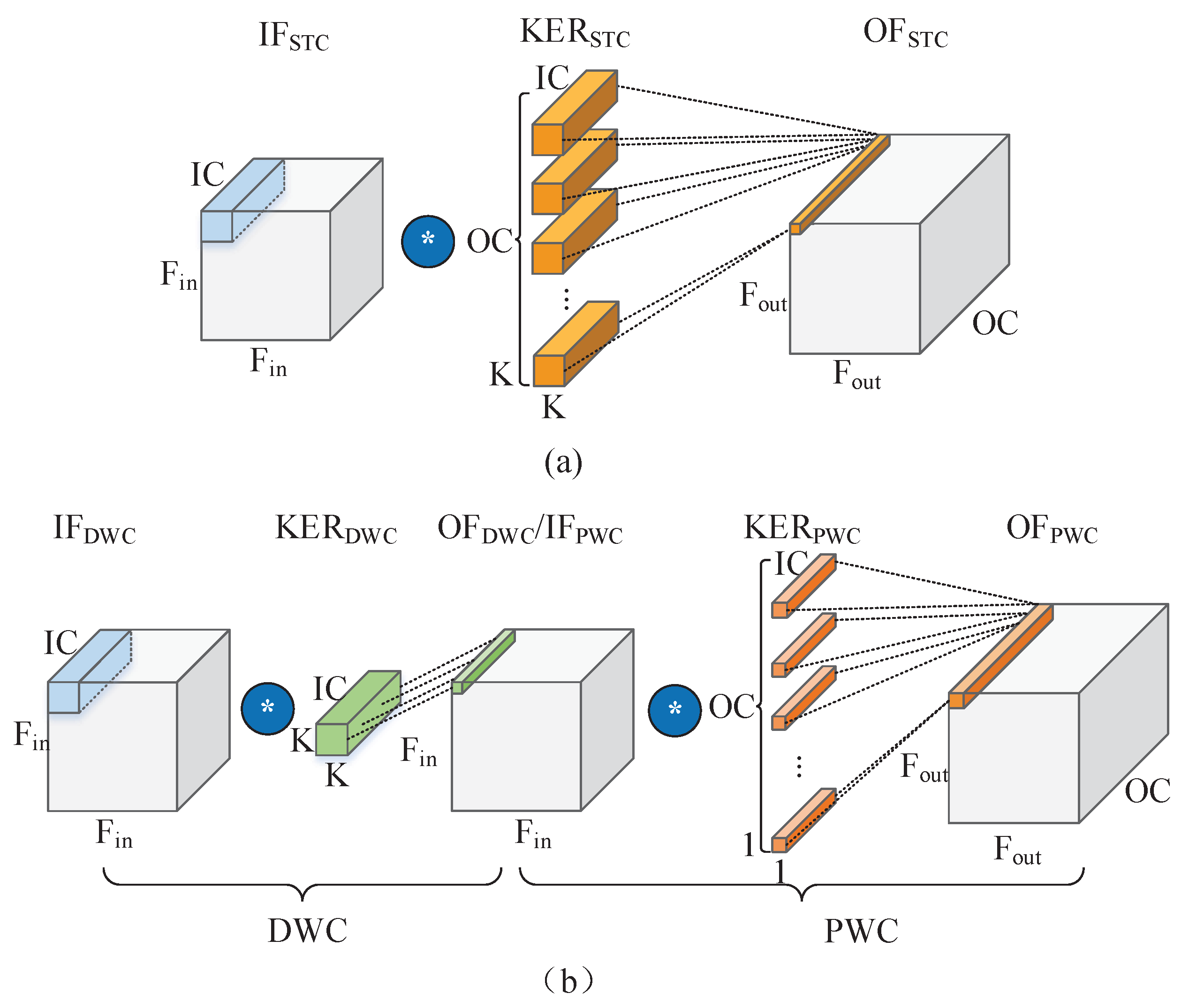
Network pruning and quantization were first proposed to reduce the computational complexity and resource consumption of deep networks. Subsequently, lightweight designs for the convolutional structure itself, such as depthwise separable convolution [4] and group convolution, have been widely used. Compared to group convolution, DSC has higher efficiency due to fewer parameters and floating operations [5], and is the most popular lightweight design method for CNN models to our knowledge.
DSC-based CNN models are being used extensively in mobile terminals, placing new demands on the power consumption and computing power of the platforms. GPUs offer excellent intensive computing performance and are often used to implement traditional convolutional accelerators. However, power consumption and volume limitations make it difficult to use GPU accelerators in embedded mobile devices. In addition, DSC is greatly different from the traditional standard convolution (STC) in terms of computational structure, and the performance of GPU-based accelerators for DSC cannot reach the theoretical value due to the high MAC/FLOPs ratio of DSC [6]. The accelerators based on application-specific integrated circuits (ASICs) are designed for specific networks and offer higher processing efficiency and lower power consumption compared to GPU-based accelerators. However, the long design and iteration cycles of ASICs and the rapid iteration of network model updates make it difficult to take full advantageof ASICs. FPGAs have powerful parallel computing capabilities and can process multiple data streams simultaneously to achieve high throughput. In addition, FPGA-based accelerators have lower power consumption compared to GPU-based accelerators and shorter design cycles compared to ASIC-based accelerators. Therefore, FPGAs have attracted much attention in the implementation of various DSC-based lightweight CNN accelerators.
Limited on-chip resources and off-chip memory access bandwidth are the two major bottlenecks in implementing FPGA-based CNN accelerators. The key step in acceleration is to maximise the utilization of on-chip computing resources and off-chip access bandwidth, and reduce the utilization of on-chip memory resources. Pipelining is a common technique for accelerating algorithms in FPGAs, and DSC can also be accelerated by using pipelined hardware structures. Ref. [7] proposes an FPGA-based DSC accelerator with all the layers working concurrently in a pipelined fashion to improve the system throughput and performance. However, only a small 10-layer DSC model was deployed on FPGAs in Ref. [7]. In fact, DSC-based networks typically have extremely deep network depth and high complexity, such as MobilenetV2 which is a 54-layer network. When a deep DSC model is deployed by using a fully pipelined architecture, the computational resources consumed will be significantly higher. In response to this problem, partial pipeline structures are widely used. Ref. [8] proposes to design a separate DWC engine in addition to the STC engine. By optimising the scheduling strategy, the two engines can operate efficiently in a pipelined fashion, and the engine size is planned according to the difference in computation volume between the different layers. However, since there are multiple engines in the accelerator, including the STC engine, DWC engine, pooling engine, and elementwise engine, when switching between different types of layers, it is not guaranteed that all engines work in parallel in a pipeline fashion, which will lead to some engines being idle. Ref. [9] uses a single PWC accelerator and a DWC accelerator individually. The DWC accelerator can be pipelined after the PWC accelerator, or it can bypass the PWC convolution accelerator to match the DWC in MobileNets, reducing off-chip memory accesses and increasing inference speed. However, some engines will be idle when the computation does not satisfy the order in which the PWC layer is computed before the DWC layer, or when the PWC accelerator is bypassed. Other designs [10,11,12,13,14] that use a partially pipelined architecture have similar engine idle problems, which reduce resource utilization. In contrast to the pipeline architecture is the single-engine architecture. The single-engine architecture was originally used in standard convolutional accelerators [15], and some high-performance DSC accelerators [6,16,17,18,19] also use this architecture. Ref. [16] was the first to propose an FPGA acceleration framework for DSC, designing a computational engine with configurable modes and sizes to accommodate multiple operations, including DWC and PWC, as well as an in-channel multiplexed data caching approach that reduces off-chip memory bandwidth requirements, and finally implementing the MobileNetV2 network on an Arria10 Soc with an image classification speed of 266 FPS. However, it does not propose a solution for the first standard convolutional layer and the last fully connected layer, nor does it address how residual structures can be efficiently implemented in hardware.
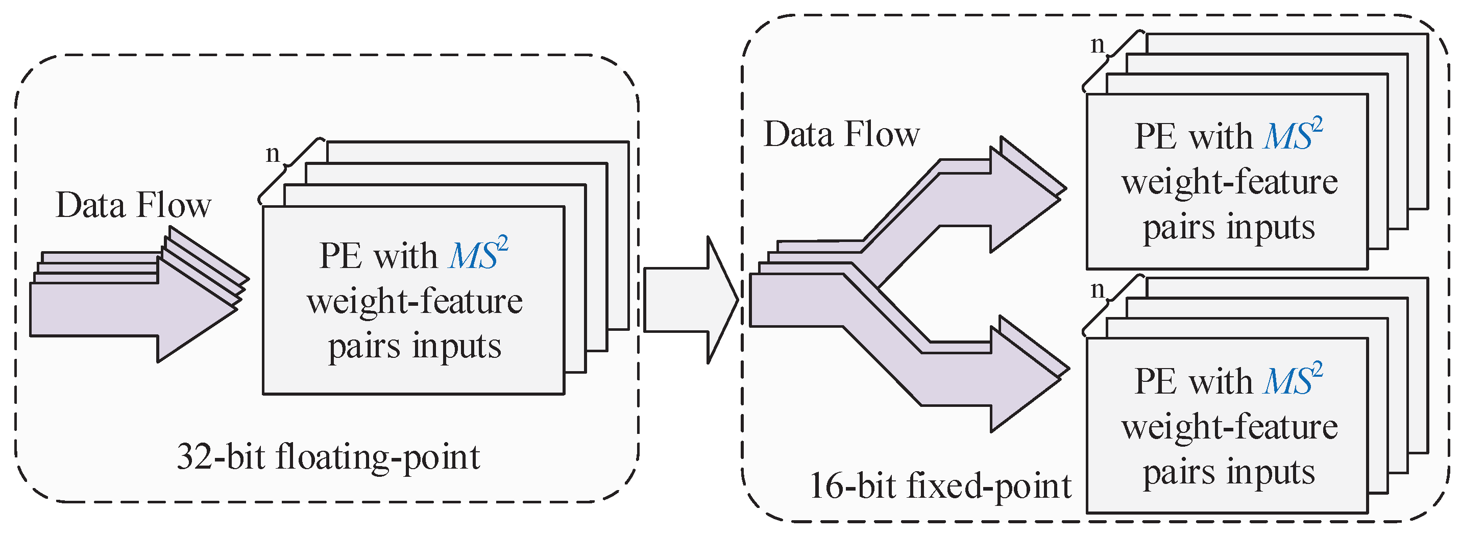
In summary, existing FPGA-based DSC accelerator designs can be divided into three categories according to the strategy of using a pipelined structure. Accordingly, there are three different strategies for designing computational engines. They are (1) a fully discrete dedicated engine design strategy, which corresponds to a fully pipelined architecture. In this architecture, each computational layer has its own dedicated engine. However, the strategy is not suitable for deep DSC networks due to the large amount of computational resources consumed. (2) The second is a partially discrete dedicated engine design strategy, which corresponds to a partially pipelined architecture. The strategy focuses on the design of PWC and DWC dedicated compute engines, as well as other types of engines. Ideally, the individual engines would be able to perform parallel computations in a pipelined fashion to reduce off-chip accesses and improve accelerator performance. However, as the accelerators switch between different types of layers, the order of the layer inputs does not match the order in which the accelerators are expected, which inevitably leads to some compute engines being idle, thus reducing resource utilization. (3) Thirdly, we have single-engine architecture. Instead of designing dedicated engines for different types of layers, multiple computations are achieved by configuring the computational modes of a single engine, which has the advantage of making full use of computational resources. However, the performance of single-engine accelerators is usually limited by the bandwidth of off-chip memory access. In addition, as the calculation process of DSC is significantly different from standard convolution, using a traditional STC engine to calculate DSC will cause the engine to idle, resulting in a waste of processing elements.
The main contributions of this work are as follows.
1.
A scalable and highly reusable multiplication and accumulation engine (MAE) is proposed to solve the engine-idling problem caused by the separate dedicated engine architecture, and the MAE is compatible with different types of computation.
2.
An efficient convolution algorithm is proposed for DWC and PWC, respectively, to reduce the on-chip memory occupancy. Meanwhile, the two algorithms achieve layer fusion between PWC and DWC and improve off-chip memory access efficiency.
3.
An address-mapping method for off-chip access is proposed. This maximises bandwidth utilization and reduces latency when reading feature maps.
The remainder of this paper is organized as follows. Section 2 briefly describes the CNN and depthwise separable convolution. Section 3 presents the design of the proposed accelerator, including the detailed computational engine design and two methods for DSC acceleration. Section 4 gives the results of the performance evaluation of the accelerator. Finally, Section 5 summarizes the content of this article.

2. Background

2.1. Convolutional Neural Network Components

CNNs are a special class of neural networks that are typically used for processing two-dimensional data such as images and video, and the core idea of the CNN is to use convolutional operations to extract spatially structured features from the input data. It usually consists of a convolutional layer, a pooling layer, an activation function layer, a fully connected layer and other structures. Several of the basic structures of CNNs mentioned in this paper are described below.

2.1.1. Convolutional Layer

The convolutional layer is used to extract features and is the most computationally intensive part of the entire network. Figure 1a shows a schematic of the convolutional computation. A convolution kernel is multiplied by the corresponding input feature window and accumulated to obtain a pixel value at the corresponding position of the output feature map. If stride is 1, the computational formula can be expressed as follows:
O F S T C ( c o , h , w ) = c i = 0 I C k 0 = 0 K k 1 = 0 K I F S T C ( c i , h + k 0 , w + k 1 ) × K E R S T C ( c o , c i , k 0 , k 1 ) + B S T C ( c o ) ,
where c o O C , h F o u t , w F o u t . I F S T C is the input feature map of size F i n × F i n × I C . K E R S T C is the convolution kernel of size K × K × I C × O C . O F S T C is the output feature map of size F o u t × F o u t × O C . B S T C is the bias of size 1 × O C .

2.1.2. Activation Function Layer

The nonlinear layer, also known as the activation function layer, acts on the output of the convolutional layer and can eliminate the linearity of the convolutional computation to reflect the deeper meaning of the network. Common activation functions can be classified into saturated activation functions including the sigmoid function, tanh function, etc., and unsaturated activation functions including the ReLU function and leaky ReLU function. For hardware deployment, unsaturated activation functions are easier to map to hardware structures and are therefore used in some lightweight neural network models. The ReLU6 function, which suppresses maximum and negative values, is primarily designed to accommodate low-precision floating-point or fixed-point computing environments. Its mathematical expression is
R e L U 6 ( x ) = m i n ( 6 , m a x ( 0 , x ) ) .

2.1.3. Global Pooling Layer

The pooling layer is used to downscale and remove redundant information. As a special type of pooling layer, the global pooling layer is usually used in the deeper layers of the network, before the fully connected layer. The global pooling layer converts a single-channel feature map of size F i n × F i n to a 1 × 1 size.

2.1.4. Fully Connected Layer

The fully connected layer maps the distributed features computed by the previous layer of the network to the corresponding sample labels. The fully connected layer is computed in a similar way to the convolutional layer and can be seen as a 1 × 1 sized convolutional kernel convolving a 1 × 1 sized feature map.

2.2. Depthwise Separable Convolution

Depthwise separable convolution is a form of factorized convolution which factorize a STC into a DWC and a 1 × 1 convolution called a PWC [20]. Whereas STC filters the inputs and combines them into a new set of outputs in one step, DSC splits this operation into two steps. In DWC, the input data is first grouped by channels, and each group undergoes a convolution operation. Subsequently, PWC is employed to combine the results from different channels.
A comparison of the computational flow of STC and DSC is shown in Figure 1. STC sums the multiplication results of the input feature (IF) and the convolution kernel (KER) of I C channels to obtain a output feature (OF) of single channel, while DWC only sums the multiplication results of a single channel to obtain the output feature of the same channel. PWC can be considered as an STC with a special convolution kernel size of 1 × 1 .
Assuming the size of the input feature map is F i n × F i n × I C , the convolution kernel size is K × K × I C × O C , and the stride is 1. The total weights and the total multiplication operations of the STC can be represented as follows, respectively:
W S T C = K × K × I C × O C
M U L T S T C = K × K × F i n × F i n × I C × O C .
The total weights and total multiplication operations of the DSC are
W D S C = K × K × I C + I C × O C
M U L T D S C = K × K × F i n × F i n × I C + F i n × F i n × I C × O C .
The ratio of DSC over STC on weights, multiplication operations are calculated as follows:
R W = W D S C W S T C = 1 O C + 1 K 2
R M U L T = M U L T D S C M U L T S T C = 1 O C + 1 K 2 .
From Equations (7) and (8), it can be seen that the DSC can significantly reduce the number of weights and the computational complexity of convolution compared to the standard convolution. Therefore, it has been used by many excellent lightweight CNN models [20,21,22,23,24,25,26].

3. Design of Accelerator

3.1. Overall Architecture

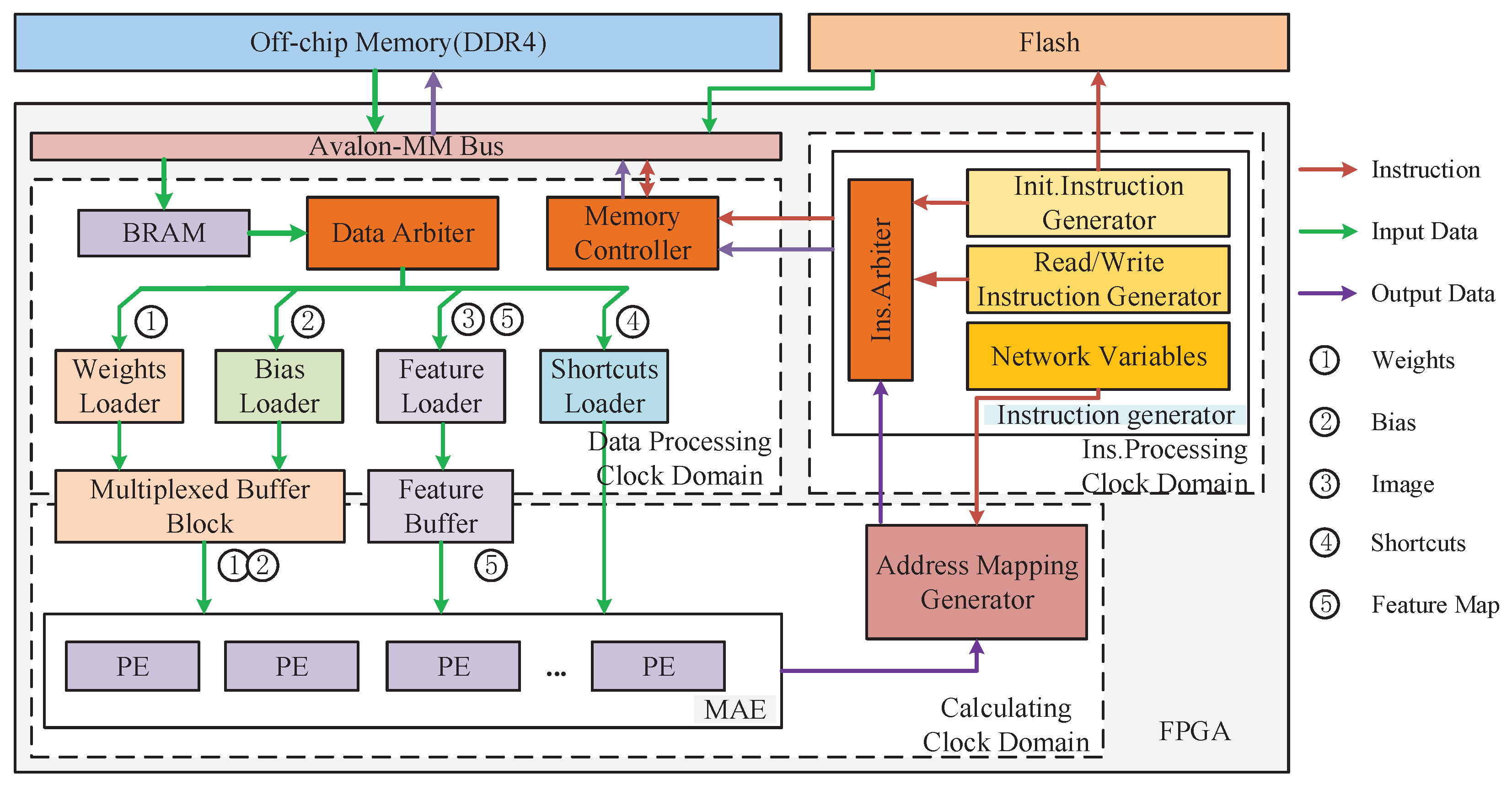
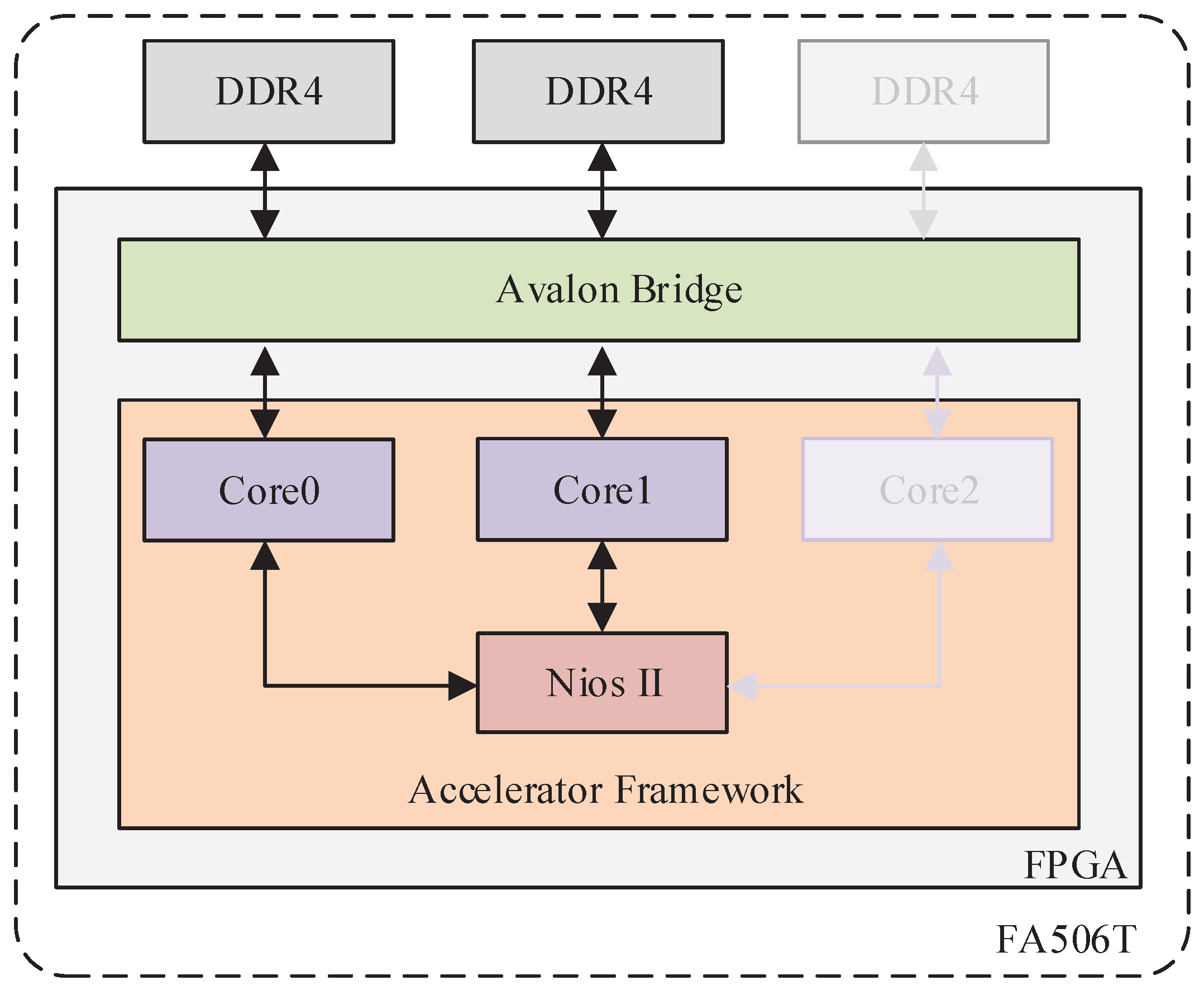
The overall architecture of the proposed accelerator is shown in Figure 2, which details the main modules and the flow of instructions and data.
When the accelerator is started, the initialization instructions will first be generated by the Init Instruction Generator, and then the network weights and biases are read from external flash into on-chip memory. Simultaneously, the address mapping generator is initialized according to preset network variables. Then, the reading feature instruction is generated by the reading instruction generator, which acts on the memory controller. The latter sends a read instruction via the Avalon-MM bus to the off-chip memory, which returns the data after several clock cycles in a pipelined fashion. All read data is buffered in the BRAM and distributed to different buffers by the data arbiter. When the biases, weights, and input features are ready, convolution calculation is preformed by MAE, and the output features are written back to DDR4 via the address-mapping generator. Write feature instructions are generated by the write instruction generator and the write process is similar to the read process. Arbitration between different instructions is performed by the ins arbiter. For framework compatibility and portability considerations, the system is divided into three clock domains including the data processing clock domain, calculating clock domain, and instruction processing clock domain. The calculating clock domain is tuned to the performance of the hardware platform.

3.2. The Scalable Multiplication and Accumulation Engine

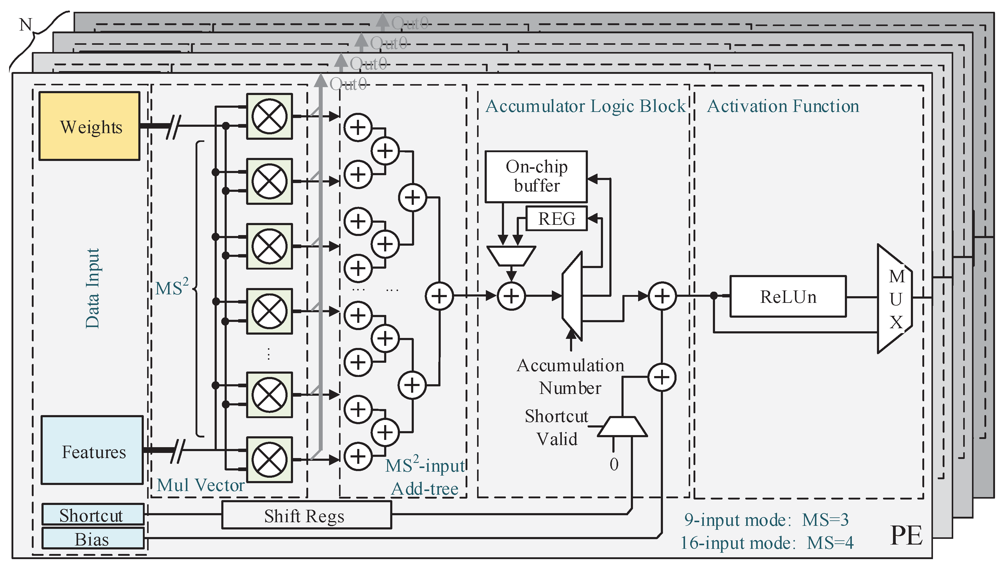
To address the problem of low utilization of computational resources caused by idle engines during the running phrase, we propose a multiplexed scalable multiplication and accumulation engine that is compatible with multiple types of computation. In this section, the structure and variable parameters of the proposed calculation engine are explained in detail. In addition, the utilization of the engine for different calculations is analysed.
The block diagram of the proposed MAE with N processing elements (PEs) is shown in Figure 3. Each PE in the MAE contains a multiplication vector with M S 2 multipliers, an add tree with M S 2 inputs, an accumulator logic block, two adders for bias and residual summation, and a ReLUn (e.g., ReLU6) logic block. N PEs are used in parallel in each MAE. The proposed MAE is scalable in size and can be adapted to various FPGA platforms with different amounts of resources by configuring M S and N. For M S , two modes are available— M S = 3 and M S = 4 —and the default is M S = 4 . Since 3 × 3 is a common convolution kernel size in CNNs, and for DSC-based CNNs (e.g., MobilenetV2), the number of channels of the feature map is usually an integer multiple of 16, the modes M S 2 = 9 and M S 2 = 16 are more friendly for PWC and DWC. A discussion of the utilization of the proposed MAE will follow below. In addition, resource utilization and accelerator performance can be easily balanced by adjusting the number of PEs, and the default is N = 16 .
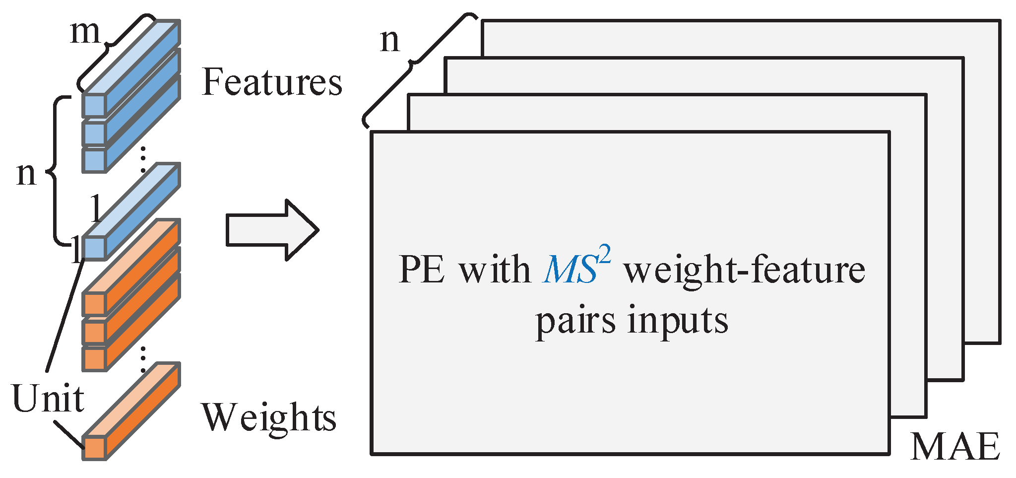
The input of each PE consists of M S 2 weight feature pairs, an inverse residual, and a bias. Assume that the number of weight feature pairs required by a valid output of PE in a single convolution calculation is M. M is equal to K × K for DWC and I C for PWC. The accumulation number of the accumulator logic block is determined by M and M S and can be expressed as
A = M M S 2 ,
where represents the operation of rounding up. The accumulator logic block works continuously, and intermediate data is temporarily cached in REG or on-chip buffer as shown in Figure 3. Compared to REG, the on-chip buffer requires more memory resources and can cache more data. Normally, the DWC calculation uses REG to accumulate directly, and part of the PWC is temporarily stored in the on-chip buffer, because the size K of the DWC filter is usually fixed and relatively small, and the channel depth I C of the PWC filter is a dynamic value and relatively large. For DWC with a fixed K × K convolution kernel, the default accumulation number is
A D W C = K 2 M S 2 .
As for PWC, I C is a dynamic variable that varies from layer to layer, and the preset accumulation number is
A P W C = I C M S 2 .
The sum of the shortcut and bias is strictly aligned with the time sequence output of the of the accumulator. In the layer without inverse residuals, the shortcuts are set to zero. The ReLUn logic block is implemented by two comparators. It is worth noting that ReLUn is placed at the end of each layer, while the inverse residual is placed before RelUn. The inverse residual is a spanning summation operation between layers. In terms of execution order, the inverse residual is usually executed after ReLUn, while in the proposed MAE the inverse residual summation is deployed before ReLUn. This is because in a number of DSC-based CNNs (e.g., MobileNetV3), ReLUn appears only within the bottleneck block, while the inverse residual summation appears after the output layer of the bottleneck block. Thus, ReLUn and inverse residual summation do not appear simultaneously. Therefore, the proposed MAE prioritises the residual summation to reduce the number of pipelines.
The different types of computation are prenormalised to DWC and PWC before the computation starts. The STC filter of size K × K × I C is replaced by the PWC filter of size 1 × 1 × I C × K 2 . Like STC, the FCL and GPL layers are also suitable to deployment as a PWC layer. The role of the softmax layer is to assign class labels based on probabilities. Since class labels are assigned by sorting the FCL output, which is less computationally intensive, softmax is not deployed on the accelerator. Note that if necessary, softmax can be implemented quickly on a Nios II processor. Batch normalization can be merged into the weight and bias of the convolution layer, which is a common method [27,28]. In addition, the inverse residual, which can be called a shortcut, should also be merged into the bias because it always lags the convolution calculation.
We analyze the scalable parameters M S and N by calculating the MAE utilization. In the proposed MAE, the multipliers and adders are approximately equal in number, and the PE utilization for convolution (e.g., DWC or PWC) can be represented by the valid multiplication load percentage. For the MAE to work properly, a zero-fill complement to PE is required for layers where the total number of multiplications is not an integer multiple of M S 2 , and the zero-fill multiplication is referred to as an invalid multiplication load. If the stride is 1, the MAE utilization for DWC and PWC with the convolution order proposed in Section 3.3 can be expressed as
U D W C = I C × K 2 × F i n 2 I C N × N × K 2 M S 2 × M S 2 × F i n 2
U P W C = I C × O C × F i n 2 I C M S 2 × M S 2 × O C N × N × F i n 2 .
According to Equations (12) and (13), both U D W C and U P W C are independent of the size of the input feature map. U D W C is related to I C and K, and U D W C reaches its maximum value when I C is an integer multiple of N and K 2 is an integer multiple of M S 2 . U P W C is determined by I C and O C , and the MAE utilization for PWC is highest when I C is an integer multiple of M S 2 and O C is an integer multiple of N. We determined the default values of M S and N by analyzing I C , O C and K of MobilenetV1, MobilenetV2, and MobilenetV3.

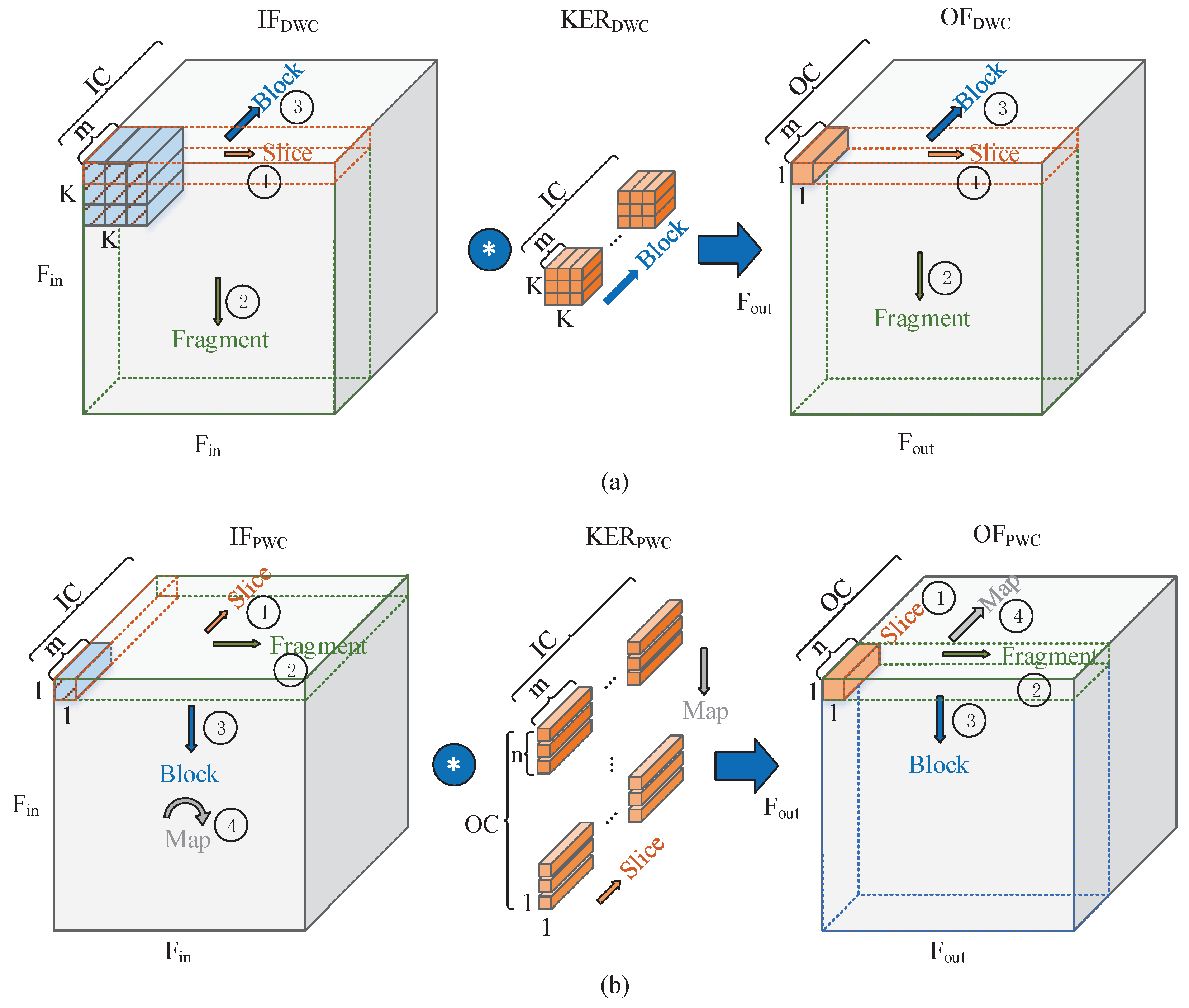
3.3. Two Efficient Convolution Algorithms

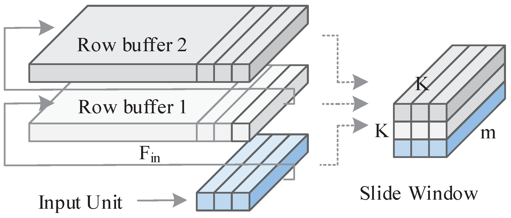
Reducing on-chip memory and improving off-chip memory access efficiency are two other focuses of this paper in addition to improving the engine utilization. In this section, we first analyse the on-chip memory resources required for four common DSC computation sequences based on the minimum cache and access cells shown in Figure 4. Subsequently, an efficient convolution algorithm is designed for DWC and PWC, respectively, under the condition of minimising on-chip memory to improve the PWC layer writing DDR4 efficiency and reduce the latency of reading feature maps.
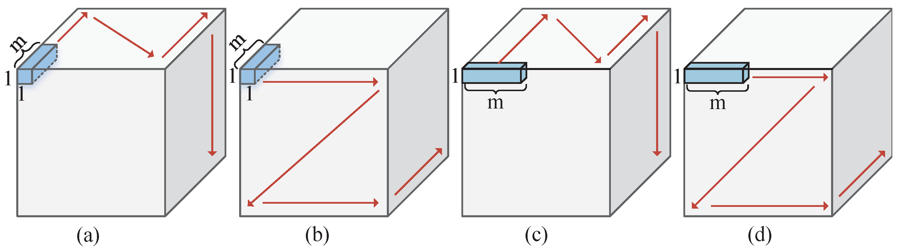
Assume that the minimum cache and access unit for feature maps and weights contains m data, and n units are filled into n PEs in parallel, as shown in Figure 4. Furthermore, the unit consisting of m interchannel data is called a pointwise unit (PU), as shown in Figure 5a,b, while the unit containing m intrachannel data is called a depthwise unit (DU), as shown in Figure 5c,d. Similarly, the interchannel first loop order is called pointwise loop (PL), as represented by the red arrows in Figure 5a,c, and the intrachannel first loop order is called depthwise loop (DL), as represented by the red arrows in Figure 5b,d.
The cached data mainly includes input feature maps and weights, and compared to the former the latter is less and occupies a smaller cache, so the input feature map cache size is mainly considered. In order to avoid frequent updating of the weight buffer, both DWC and PWC multiplex the weight data. The DWC features of different input channels are filled into respective PEs, while the PWC features of different input channels are filled into the same PE. Take DWC with PUDL convolution order, as shown in Figure 5b, as an example. We use the structure shown in Figure 6 to perform the sliding window operation. The minium cache size of input features before starting convolution calculation is
B U F D W C ( P U D L ) = ( F i n × ( K 1 ) + K ) × m × Q ,
where Q is the quantified bit width. Similarly, the cache size of DWC and PWC with the various convolution orders are calculated, and the results are shown in Table 1. Compared to F i n and I C , m, n and K are usually taken as smaller values. Thus, by analyzing Table 1, it is clear that for DWC, the PUDL convolution order requires the smallest buffer size. For PWC, the PUDL convolution order requires the same buffer size as PUPL and is smaller than the other two orders. However, the PWC calculation with PUDL order requires additional resource to store intermediate results and a more complex control strategy compared to with PUPL order. Therefore, in terms of the minimum preconvolution feature cache size, PUPL is the most efficient convolution order for PWC. In summary, the use of the PUDL order to calculate DWC, along with the PUPL order to calculate PWC, can minimize the preconvolution feature cache size.
In addition, although the use of the above two convolution orders can effectively reduce on-chip memory, the proposed MAE using a unified architecture requires a large number of off-chip memory accesses [5], which can negatively impact the overall performance of the accelerator. On the other hand, with the advancement of semiconductor processes and architecture design, the data transfer rate of double data rate SDRAM has reached a considerable level. Sequential reads or writes make efficient use of DDR4 bandwidth, whereas random reads or writes can negatively affect the use of DDR4 bandwidth. We found that the DSC accelerator can only access the DDR4 with a relatively small burst length in most cases because the output order of the feature map of the previous layer is different from the input order of the feature map of the next layer. Therefore, by designing the convolution order to achieve partial fusion between PWC and DWC, the burst length of DDR4 accesses can be improved, which in turn improves the overall performance of the proposed DSC accelerator. Based on the above analysis, we designed an efficient convolution order for DWC and PWC, respectively.
Figure 7 shows the diagram of the two proposed efficient convolution orders, which can achieve partial fusion of PWC and DWC. For presentation purposes, the input feature maps are divided into S l i c e , F r a g m e n t , B l o c k , and M a p based on the minimum cache and access unit, which is shown in Figure 4. D W C P U D L uses the order of PUDL for the computation, and the detailed algorithm is shown in Algorithm 1. The input features and weights are stored in the multiplexed buffer block and feature buffer, respectively, as shown in Figure 2. By default, m is equal to n. The m data in each PU are filled into n PEs separately, and the calculation starts when each PE is filled with K × K data. If K × K is not divisible by M S 2 , when K × K is less than M S 2 , zero is filled to make up the inputs, and when K × K is greater than M S 2 , the calculation is split into multiple times.
Algorithm 1: DWC calculation with PUDL convolution order.
Electronics 12 01571 i001
Similarly, P W C P U P L uses the order of PUPL for the calculation, and the Algorithm 2 shows the details. m × n weights are first stored in the multiplexed buffer block. When the feature buffer is fully filled with m input features which come from the same PU, the PU is copied n times to form m × n weight feature pairs with the preprepared weights, and the weight feature pairs are then filled with n PEs. The m data which from the same PU are filled into the same PE, and the inputs are supplemented to M S 2 by a similar way as D W C P U D L . When I C is greater than M S 2 , the calculation is split into multiple times.
Algorithm 2: PWC calculation with PUPL convolution order.
Electronics 12 01571 i002
Moreover, the output order of F r a g m e n t of P W C P U P L is the same as the input order of S l i c e of D W C P U D L . Therefore, the output of P W C P U P L can be written to consecutive DDR4 memory cells with a large burst length. This approach reduces the latency of DDR4 accesses and improves the performance of the proposed accelerator.

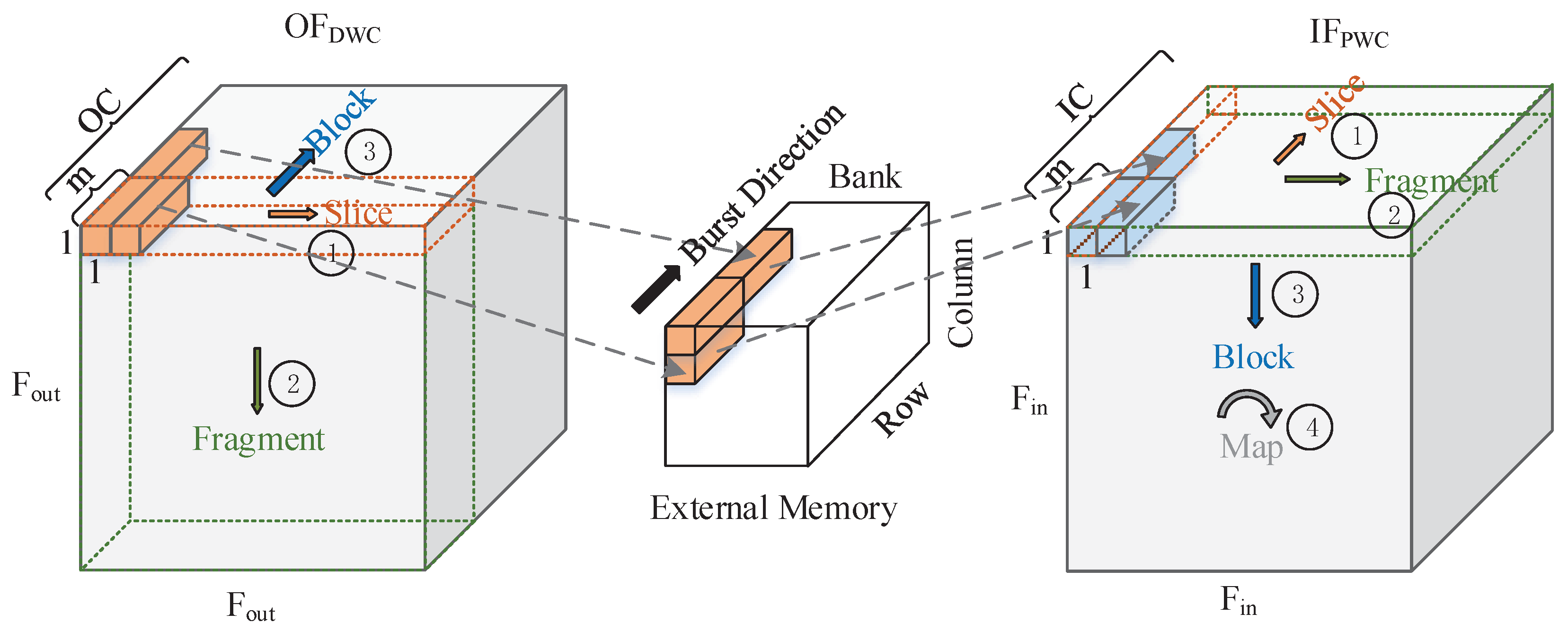
3.4. Address-Mapping Method

Although the off-chip memory access efficiency is improved by designing the P W C P U P L and D W C P U D L convolution orders, it is still limited by the reading burst length when switching from the D W C P U D L to the P W C P U P L layer. In this section, we first analyse the reasons for the constrained read burst length of the P W C P U P L layer, and then propose an address-mapping method for the output feature map in off-chip memory to maximize bandwidth utilization when reading the features of P W C P U P L layer.
As mentioned earlier, the reason for the low DDR4 access efficiency when switching from D W C P U D L to P W C P U P L is that the output order of the former is different from the input order of the latter. If the output features are written directly to off-chip memory in the default D W C P U D L output order, there are two scenarios when reading the input features required by P W C P U P L from external memory.
  • Input features are read into the accelerator from off-chip memory at large burst lengths from contiguous addresses, where the data is contiguous but must be heavily cached on-chip because the data order does not match the expected input order of the P W C P U P L .
  • Input features are read into the accelerator from discrete external memory cells at a small burst length, where the data order matches the desired computational order of the P W C P U P L but the off-chip memory access is inefficient.
Neither of above two scenarios can achieve a balance between on-chip memory and off-chip memory access efficiency. Considering that when accelerating DSC, the same output feature map is only written to DDR4 once, while the same input feature map needs to be read out of DDR4 one or more times, the bandwidth gain from read optimization of the feature map data is greater than that from write optimization. Therefore, the address mapping method is designed to allow external memory to be read in efficient sequential bursts without requiring large amounts of on-chip memory resources. As shown in Figure 8, the DWC outputs features in the order of PUDL, while the next layer of PWC reads features in the order of PUPL. Usually, the output features of D W C P U D L are by default stored in continuous external memory cells along the burst direction, while in the proposed method they are stored in discrete cells according to precalculated addresses, while ensuring that the input features of P W C P U P L can be accessed in the expected input order at large burst lengths. Assuming that the minimum cache and access unit still consists of m data and the counts in the three dimensions of O F D W C are s l i c e , f r a g and b l o c k , the offset address of each D W C P U D L output unit is expressed as
A D D R o f f s e t = O C m × ( F i n × ( f r a g 1 ) + ( s l i c e 1 ) ) + b l o c k .
The address-mapping method above describes the relationship between the feature output order and the offset address of each D W C P U D L output unit. At the stage of writing back to off-chip memory, the final address must be calculated based on the stored base address of the current layer, and the final address can be expressed as
A D D R f i n a l = B A l + A D D R o f f s e t ,
where B A l is the base address of the current layer. The number of off-chip memory addresses occupied by each feature matrix is equal to the total number of units contained in the features of that layer. Therefore, the base address of each layer can be calculated by accumulating layer by layer, and can be quickly obtained by looking up the table.

4. Evaluation

4.1. Implementation Consideration

To evaluate the accelerator, we first verified the simulation. MobileNetV2-1.0-224 was run on Matlab, and all intermediate features were saved layer by layer as standard results. Next, the accelerator architecture was simulated with VCS and Verdi, and all effective outputs of the MAE were compared with the standard results. After ensuring a characteristic error of almost zero, the accelerator was deemed to operate normally. Finally, synthesis and power consumption estimation were carried out with Quartus Prime 18.1 Pro. Due to time and personnel constraints, we have completed partial hardware deployment.
Numerical precision is an extremely important factor that directly affects the throughput and inference accuracy of accelerator. Using a lower-precision bit width can yield exponentially higher throughput and processing performance than deploying network with floating point. However, the lower numerical precision makes it difficult to meet the flexibility and compatibility when deploy networks with different quantization strategies by using the same accelerator architecture. For example, the processing element and data flow of the whole accelerator architecture may need to be modified to accommodate the new number format when changing the quantization strategy. If the numerical precision is expanded, the data flow often needs to be reconsidered, and conversely if it is reduced, compatibility can be achieved through parallel processing, as shown in Figure 9. In most FPGAs, DSPs can be flexibly configured as single floating point or double fixed point multipliers and adders, and there is virtually no increase in DSP requirements after parallelization. It is easy to be downward-compatible with lower bit width but hardly easy to be upward-compatible with higher bit width for a fixed accelerator architecture. Moreover, considering that 32-bit floating-point is the standard format for parameter training and a common format for image classification, 32-bit floating-point was chosen as the basic numerical precision of the proposed accelerator architecture, while 16-bit quantization strategy is an alternative according to the resource and the need of performance.
Furthermore, the proposed accelerator is a lightweight accelerator, so multiple parallel accelerator cores can be deployed if the FPGA resource and DDR4 bandwidth allow. A similar deployment strategy was used in Ref. [29]. We deploy two parallel floating-point accelerators according to the resource and off-chip access bandwidth of the FA506T. The block diagram of the evaluation system is shown in Figure 10. The Nios II processor is used for result processing and network configuration. The softmax layer is not implemented in accelerator, so the accelerator ends with the FCL. The Nios II receives the output from the accelerator and sorts it to obtain the final classification result. In addition, Nios II is also used to modify the parameters of the network, such as the size of the feature map. As part of the accelerator system, its resource and power consumption is retained in the evaluation.

4.2. Implementation Results

4.2.1. FPGA Resource Utilization and Burst Length

The performance of the proposed accelerator architecture is demonstrated by implementing the MobileNetV2-1.0-224 network using Verilog HDL on the Intel Arria 10 GX 660 (10AX066K3F40E2SG) FPGA, which contains 251, 680 ALMs, 2131 M20K, and 1687 DSP blocks. The proposed accelerator runs at 200 MHz, and Table 2 shows its overall resource utilization. The proposed accelerator is a lightweight accelerator and uses only 16.73% of the ALMs, as shown in Table 2, even when two accelerator cores are used simultaneously. A total of 578 of the 1118 M20Ks are used to build the weight and feature buffers, and the rest are used to synchronize the DDR4 data. A total of 1082 DSPs are used, and almost all DSPs are used to implement the floating point MAE proposed in Section 3.2.
Figure 11 shows the burst length for the reading and writing of DDR4 of each layer. By using the two convolutional algorithms proposed in Section 3.3, the output feature of the PWC can be written into contiguous DDR4 memory cells with a large burst length when switching from the PWC layer to the DWC layer. For example, when the input image size is 224 × 224 × 3 , the writing burst length is set to 32 for all PWC layers (e.g., layers 4, 7, 10, etc.) preceding the DWC layer in the first 33 layers. In contrast, the writing burst length is set to 1 for all PWC layers (e.g., layers 3, 6, 9, etc.) following the DWC layer. Similarly, by using the address mapping method proposed in Section 3.4, all PWC layers are able to read the input feature map with a large burst length. It can be seen from Figure 11 that all PWC layers have read burst lengths greater than 15, and the largest read burst length reaches 70 (e.g., layers 43, 46, 49, etc.).

4.2.2. Comparison with CPU Implementation

Figure 12 shows the total multiplication and addition of each layer of Mobilenet-1.0-224, including the calculation of the batch normalization layer. Figure 13 shows the CPU running time of each layer, obtained by calculating the average time to process 50 images consecutively. In Ref. [30], the general trend of the CPU running time curve is approximately the same as that of the total multiplication and addition curve. However, the same conclusion was not drawn from the measurements of this work. Figure 14 shows the running time of each layer on the proposed accelerator.
The version of the CPU used for testing is 12th Gen Intel(R) Core(TM) i7-12700H. Network inference and runtime measurements are based on pytorch 1.13.0 and torchvision 0.14.0. For the CPU under test, the proposed accelerator achieves a speed-up of 14 times for an image of size 224 × 224 × 3 .

4.2.3. Comparison with FPGA Implementations

Table 3 shows the performance comparison between the proposed accelerator and previous FPGA-based accelerator implementations. It can be seen that for 224 × 224 × 3 input images, our accelerator achieves a maximum inference speed of 205.1 FPS, and a maximum throughput of 128.8 GFLOPS. Moreover, most accelerators use fixed 16-bit or even lower precision, and it is unfair to compare performance based on literal values for inference speed and throughput. DSP efficiency comparisons are more intuitive for accelerator implementations that use different platforms and network architectures. For a fair comparison, the GOPS/DSP values are normalized to 16-bit, where the values for 32-bit systems are multiplied by 2, which uses the same normalization method used in Ref. [5]. It can be seen from Table 3, after normalization, our proposed accelerator has the highest DSP efficiency.
Table 4 shows the comparison of resource utilization with reference FPGA-based single-engine accelerators. For a fair comparison, we normalize the logical resource usage to the number of LUTs and FFs for accelerators using different platforms. In an Arria 10 FPGA, an ALM contains 2 LUTs and 4 regs, so the normalized number of LUTs and FFs is equal to the original number of ALMs multiplied by 2 and 4, respectively. And as can be seen from Table 4, our proposed accelerators use the least amount of logical resources after normalization. Moreover, the DSP usage and GOPS/DSP comparisons show that we use fewer DSPs and achieve higher efficiency per DSP compared to the reference design. This is due to the use of highly reusable MAEs, which greatly improves the utilization of computational resources and solves the problem of idle engines in the inference phase. In addition, the two efficient convolution algorithms proposed in Section 3.3 achieve a partial fusion of the PWC and DWC layers, which, combined with the proposed address mapping method in Section 3.4, improves off-chip memory access efficiency and reduces accelerator data access latency.

4.3. Evaluations on Other Networks

We evaluated MobileNetV3-Small based on the proposed accelerator framework. However, due to the constraints of time and the experimental platform, only the estimated results are given here. Since the main bottleneck of the single-engine architecture used in this paper is the off-chip access bandwidth, we use the total number of off-chip accesses as a measure. Assuming that each off-chip access takes one clock cycle, off-chip accesses and computations are performed in a pipelined fashion, the input image size is 224 × 224 × 3 , and the accelerator runs at 200 MHz. It can be seen from Table 5 that the proposed accelerator can also achieve a competitive acceleration result for MobileNetV3-Small.

5. Conclusions

This paper presents a high-performance FPGA-based DSC accelerator. The main objective of this paper is to solve the common engine idling problem in DSC accelerator design and to maximise the utilization of on-chip computational resources and off-chip access bandwidth. To address the engine-idle problem, we propose a scalable and highly reusable MAE to accommodate different computations including DWC, PWC, etc. Based on the proposed MAE, an efficient convolutional algorithm is proposed for DWC and PWC, respectively, to reduce the on-chip memory occupancy. At the same time, the proposed two convolutional algorithms achieve partial fusion of PWC and DWC to improve the efficiency of writing to off-chip memory. An address mapping method for off-chip access is proposed to maximise bandwidth utilization and reduce latency when reading the input feature map of the PWC layer. The performance of the proposed accelerator is demonstrated by implementing the MobileNetV2-1.0-224 network on an Intel Arria 10 GX660 FPGA. The proposed accelerator uses a 32-bit floating point and runs at 200 MHz. For an input image of size 224 × 224 × 3 , our accelerator achieves a maximum inference speed of 205.1 FPS and a maximum throughput of 128.8 GFLOPS. The accelerator achieves a 14× speed-up in inference compared to a general-purpose CPU implementation. In addition, we use DSP efficiency to measure the computational resource utilization of the FPGA-based accelerator, and the proposed accelerator has a DSP efficiency of 0.24 GOPS/DSP, which is higher than the reference design.

Author Contributions

Conceptualization, J.H. and Z.Z.; methodology, J.H. and Z.Z.; software, X.L.; validation, X.L. and T.G.; formal analysis, X.L.; investigation, T.G.; data curation, X.L.; writing—original draft preparation, X.L.; writing—review and editing, J.H.; supervision, J.H.; project administration, J.H.; All authors have read and agreed to the published version of the manuscript.

Funding

This research was funded in part by the National Natural Science Foundation of China under Grants U19B2016.

Institutional Review Board Statement

Not applicable.

Informed Consent Statement

Not applicable.

Data Availability Statement

Not applicable.

Conflicts of Interest

The authors declare no conflict of interest.

References

  1. Chen, L.; Li, S.; Bai, Q.; Yang, J.; Jiang, S.; Miao, Y. Review of Image Classification Algorithms Based on Convolutional Neural Networks. Remote Sens. 2021, 13, 4712. [Google Scholar] [CrossRef]
  2. Wang, Y.; Zhang, W.; Gao, R.; Jin, Z.; Wang, X. Recent advances in the application of deep learning methods to forestry. Wood Sci. Technol. 2021, 55, 1171–1202. [Google Scholar] [CrossRef]
  3. Guo, Z.; Huang, Y.; Hu, X.; Wei, H.; Zhao, B. A Survey on Deep Learning Based Approaches for Scene Understanding in Autonomous Driving. Electronics 2021, 10, 471. [Google Scholar] [CrossRef]
  4. Sandler, M.; Howard, A.; Zhu, M.; Zhmoginov, A.; Chen, L.C. Mobilenetv2: Inverted residuals and linear bottlenecks. In Proceedings of the IEEE Conference on Computer Vision and Pattern Recognition, Salt Lake City, UT, USA, 18–23 June 2018; pp. 4510–4520. [Google Scholar]
  5. Li, B.; Wang, H.; Zhang, X.; Ren, J.; Liu, L.; Sun, H.; Zheng, N. Dynamic Dataflow Scheduling and Computation Mapping Techniques for Efficient Depthwise Separable Convolution Acceleration. IEEE Trans. Circuits Syst.-Regul. Pap. 2021, 68, 3279–3292. [Google Scholar] [CrossRef]
  6. Li, G.; Zhang, J.; Zhang, M.; Wu, R.; Cao, X.; Liu, W. Efficient depthwise separable convolution accelerator for classification and UAV object detection. Neurocomputing 2022, 490, 1–16. [Google Scholar] [CrossRef]
  7. Ding, W.; Huang, Z.; Huang, Z.; Tian, L.; Wang, H.; Feng, S. Designing efficient accelerator of depthwise separable convolutional neural network on FPGA. J. Syst. Archit. 2019, 97, 278–286. [Google Scholar] [CrossRef]
  8. Wu, D.; Zhang, Y.; Jia, X.; Tian, L.; Li, T.; Sui, L.; Xie, D.; Shan, Y. A high-performance CNN processor based on FPGA for MobileNets. In Proceedings of the 2019 29th International Conference on Field Programmable Logic and Applications (FPL), Barcelona, Spain, 8–12 September 2019; pp. 136–143. [Google Scholar]
  9. Lin, Y.; Zhang, Y.; Yang, X. A Low Memory Requirement MobileNets Accelerator Based on FPGA for Auxiliary Medical Tasks. Bioengineering 2023, 10, 28. [Google Scholar] [CrossRef] [PubMed]
  10. Liu, X.; Yang, J.; Zou, C.; Chen, Q.; Yan, X.; Chen, Y.; Cai, C. Collaborative Edge Computing With FPGA-Based CNN Accelerators for Energy-Efficient and Time-Aware Face Tracking System. IEEE Trans. Comput. Soc. Syst. 2022, 9, 252–266. [Google Scholar] [CrossRef]
  11. Shang, J.; Zhang, K.; Zhang, Z.; Li, C.; Liu, H. A high-performance convolution block oriented accelerator for MBConv-Based CNNs. Integr.-Vlsi J. 2023, 88, 298–312. [Google Scholar] [CrossRef]
  12. Wang, X.; Tian, T.; Zhao, L.; Wu, W.; Jin, X. Exploration of Balanced Design in Resource-Constrained Edge Device for Efficient CNNs. IEEE Trans. Circuits Syst.-Express Briefs 2022, 69, 4573–4577. [Google Scholar] [CrossRef]
  13. Choi, K.; Sobelman, G.E. An Efficient CNN Accelerator for Low-Cost Edge Systems. ACM Trans. Embed. Comput. Syst. 2022, 21, 44. [Google Scholar] [CrossRef]
  14. Xuan, L.; Un, K.F.; Lam, C.S.; Martins, R.P. An FPGA-Based Energy-Efficient Reconfigurable Depthwise Separable Convolution Accelerator for Image Recognition. IEEE Trans. Circuits Syst.-Express Briefs 2022, 69, 4003–4007. [Google Scholar] [CrossRef]
  15. Yu, X.; Wang, Y.; Miao, J.; Wu, E.; Zhang, H.; Meng, Y.; Zhang, B.; Min, B.; Chen, D.; Gao, J. A data-center FPGA acceleration platform for convolutional neural networks. In Proceedings of the 2019 29th International Conference on Field Programmable Logic and Applications (FPL), Barcelona, Spain, 8–12 September 2019; pp. 151–158. [Google Scholar]
  16. Bai, L.; Zhao, Y.; Huang, X. A CNN Accelerator on FPGA Using Depthwise Separable Convolution. IEEE Trans. Circuits Syst.-Express Briefs 2018, 65, 1415–1419. [Google Scholar] [CrossRef] [Green Version]
  17. Fan, H.; Liu, S.; Ferianc, M.; Ng, H.C.; Que, Z.; Liu, S.; Niu, X.; Luk, W. A real-time object detection accelerator with compressed SSDLite on FPGA. In Proceedings of the 2018 International Conference on Field-Programmable Technology, Naha, Japan, 10–14 December 2018; pp. 14–21. [Google Scholar]
  18. Liang, Y.; Lu, L.; Jin, Y.; Xie, J.; Huang, R.; Zhang, J.; Lin, W. An Efficient Hardware Design for Accelerating Sparse CNNs With NAS-Based Models. IEEE Trans.-Comput.-Aided Des. Integr. Syst. 2022, 41, 597–613. [Google Scholar] [CrossRef]
  19. Chang, L.; Zhang, S.; Du, H.; Chen, Y.; Wang, S. A Reconfigurable Neural Network Processor With Tile-Grained Multicore Pipeline for Object Detection on FPGA. IEEE Trans. Very Large Scale Integr. (Vlsi) Syst. 2021, 29, 1967–1980. [Google Scholar] [CrossRef]
  20. Howard, A.G.; Zhu, M.; Chen, B.; Kalenichenko, D.; Wang, W.; Weyand, T.; Andreetto, M.; Adam, H. Mobilenets: Efficient convolutional neural networks for mobile vision applications. arXiv 2017, arXiv:1704.04861. [Google Scholar]
  21. Howard, A.; Sandler, M.; Chu, G.; Chen, L.C.; Chen, B.; Tan, M.; Wang, W.; Zhu, Y.; Pang, R.; Vasudevan, V.; et al. Searching for mobilenetv3. In Proceedings of the IEEE/CVF International conference on Computer Vision, Seoul, Republic of Korea, 27 October 2019–2 November 2019; pp. 1314–1324. [Google Scholar]
  22. Zhang, X.; Zhou, X.; Lin, M.; Sun, J. Shufflenet: An extremely efficient convolutional neural network for mobile devices. In Proceedings of the IEEE Conference on Computer Vision and Pattern Recognition, Salt Lake City, UT, USA, 18–23 June 2018; pp. 6848–6856. [Google Scholar]
  23. Ma, N.; Zhang, X.; Zheng, H.T.; Sun, J. Shufflenet v2: Practical guidelines for efficient cnn architecture design. In Proceedings of the European Conference on Computer Vision (ECCV), Munich, Germany, 8–14 September 2018; pp. 116–131. [Google Scholar]
  24. Tan, M.; Le, Q. Efficientnet: Rethinking model scaling for convolutional neural networks. In Proceedings of the International Conference on Machine Learning, PMLR, Long Beach, CA, USA, 9–15 June 2019; pp. 6105–6114. [Google Scholar]
  25. Tan, M.; Le, Q. Efficientnetv2: Smaller models and faster training. In Proceedings of the International Conference on Machine Learning, PMLR, Virtual, 18–24 July 2021; pp. 10096–10106. [Google Scholar]
  26. Chollet, F. Xception: Deep learning with depthwise separable convolutions. In Proceedings of the IEEE Conference on Computer Vision and Pattern Recognition, Honolulu, HI, USA, 21–26 July 2017; pp. 1251–1258. [Google Scholar]
  27. Fan, H.; Luo, C.; Zeng, C.; Ferianc, M.; Que, Z.; Liu, S.; Niu, X.; Luk, W. F-E3D: FPGA-based acceleration of an efficient 3D convolutional neural network for human action recognition. In Proceedings of the 2019 IEEE 30th International Conference on Application-Specific Systems, Architectures and Processors (ASAP), New York, NY, USA, 15–17 July 2019; Volume 2160, pp. 1–8. [Google Scholar]
  28. Ma, Y.; Suda, N.; Cao, Y.; Seo, J.s.; Vrudhula, S. Scalable and modularized RTL compilation of convolutional neural networks onto FPGA. In Proceedings of the 2016 26th International Conference on Field Programmable Logic and Applications (FPL), Lausanne, Switzerland, 29 August–2 September 2016; pp. 1–8. [Google Scholar]
  29. Knapheide, J.; Stabernack, B.; Kuhnke, M. A high throughput MobileNetV2 FPGA implementation based on a flexible architecture for depthwise separable convolution. In Proceedings of the 2020 30th International Conference on Field-Programmable Logic and Applications (FPL), Gothenburg, Sweden, 31 Augus–4 September 2020; pp. 277–283. [Google Scholar]
  30. Liu, B.; Zou, D.; Feng, L.; Feng, S.; Fu, P.; Li, J. An FPGA-Based CNN Accelerator Integrating Depthwise Separable Convolution. Electronics 2019, 8, 281. [Google Scholar] [CrossRef] [Green Version]
Figure 1. Comparison of the computational flow of STC and DSC. (a) The computational flow of standard convolution. (b) The computational flow of depthwise separable convolution. (∗) represents the operation of convolution.
Electronics 12 01571 g001
Figure 2. The overall architecture of the proposed accelerator.
Electronics 12 01571 g002
Figure 3. Block diagram of multiplication and accumulation engine.
Electronics 12 01571 g003
Figure 4. The schematic of minimum cache and access units.
Electronics 12 01571 g004
Figure 5. Four convolution orders based on the minimum cache and access unit. (a) The convolution order with pointwise unit and pointwise loop (PUPL). (b) The convolution order with pointwise unit and depthwise loop (PUDL). (c) The convolution order with depthwise unit and pointwise loop (DUPL). (d) The convolution order with depthwise unit and depthwise loop (DUDL).
Electronics 12 01571 g005
Figure 6. The line buffers for DWC with PUDL convolution order.
Electronics 12 01571 g006
Figure 7. The diagram of convolution order for D W C P U D L and P W C P U P L . By default, m is equal to n. (a) DWC calculation using pointwise unit and depthwise loop. K × K × m weights are stored in the on-chip buffer, and are updated after the calculation of a F r a g m e n t . Input feature maps need to be read only once. (b) PWC calculation using pointwise unit and pointwise loop. The weights are stored in on-chip buffer and updated to another n × I C after the calculation of each M a p . Input feature maps need to be read multiple times. (∗) represents the operation of convolution.
Electronics 12 01571 g007
Figure 8. The address mapping between the output unit of D W C P U D L and the input unit of P W C P U P L .
Electronics 12 01571 g008
Figure 9. Parallelization-compatible processing method after data bit width is reduced.
Electronics 12 01571 g009
Figure 10. Block diagram of the evaluation system. The number of accelerator cores is configurable, which is determined by FPGA resource and off-chip access bandwidth.
Electronics 12 01571 g010
Figure 11. Burst length for the reading and writing of DDR4 of each layer.
Electronics 12 01571 g011
Figure 12. Total multiplication and addition of each layer.
Electronics 12 01571 g012
Figure 13. CPU running time of each layer.
Electronics 12 01571 g013
Figure 14. Accelerator running time of each layer.
Electronics 12 01571 g014
Table 1. The minimum preconvolution feature cache size and output order for DWC and PWC with various convolution orders.
Convolution OrderConvolution TypeMinimum Cache Size (bit)Output Order
PUPLDWC ( ( F i n + 1 ) × ( K 1 ) × I C + m ) × Q PUPL
PWC0PUDL
PUDLDWC ( F i n × ( K 1 ) + K ) × m × Q PUDL
PWC0PUDL
DUPLDWC ( F i n × I C × ( K 1 ) + m × n ) × Q DUPL
PWC m × n × Q PUDL
DUDLDWC ( F i n × ( F i n × ( n 1 ) + K 1 ) + m ) × Q DUDL
PWC ( F i n 2 × ( n 1 ) + m ) × Q PUDL
Table 2. FPGA resource utilization.
 ALMM20KDSP
Utilization42,116.7 (16.73%)1118 (52.46%)1082 (64.14%)
Table 3. Comparison of performance with pervious FPGA-based accelerators and traditional platforms.
WorkNetworkPlatformBit-WidthFrequency
(MHz)
FPSGOPSGFLOPSDSPDSP Efficiency 1
(GOPS/DSP)
M. Sandler’18 [4]MobileNetV2CPU--13.3----
G. Li’22 [6]MobileNetV2XC7Z10016-bit200371.4222.8-11630.19
W. Ding’19 [7]DS-CNNArria10 GX 115016-bit180-98.9-7120.14
L. Bai’18 [16]MobileNetV2Arria10 SX 66016-bit133266.2170.6-12780.13
B. Liu’19 [30]MobileNetV2Zynq 7100float 32-bit100--17.1119260.02
ProposedMobileNetV2Arria10 GX 660float 32-bit200205.1-128.810820.24
1 For a fair comparison, it is normalized to 16-bit, where the value of a 32-bit system is multiplied by 2, which uses the same normalization method as Ref. [5].
Table 4. Comparison of resource utilization with reference FPGA-based accelerators.
 L. Bai’18 [16]G. Li’22 [6]Proposed
PlatformIntel
Arria10 SX660
Xilinx
XC7Z100
Intel
Arria10 GX660
Bit width16-bit16-bitfloat 32-bit
Logic UsageALM 82KLUT 183K/FF 231KALM 42K
Normalized 1 Logic UsageLUT 164K/FF 328KLUT 183K/FF 231KLUT 84K/FF 168K
DSP Usage127811631082
Memory Usage (Mb)24.5-13.3 2
Normalized 3 Memory Usage49-13.3
GOPS/W-12.5-
GFLOPS/W--7.8
GOPS/DSP 40.130.190.24
1 An ALM in an Arria 10 FPGA contains 2 LUTs and 4 regs. 2 Total block memory bits. 3 It is nomalized to 32-bit, where the value of a 16-bit system is multiplied by 2. 4 It is nomalized to 16-bit, where the value of a 32-bit system is multiplied by 2.
Table 5. Evaluation result for MobileNetV3-Small.
NetworkBit WidthFrequency
(MHz)
Total Off-Chip Memory
Accesses (Million)
FPS
MobileNetV3-Small117.72001.80222.1
Disclaimer/Publisher’s Note: The statements, opinions and data contained in all publications are solely those of the individual author(s) and contributor(s) and not of MDPI and/or the editor(s). MDPI and/or the editor(s) disclaim responsibility for any injury to people or property resulting from any ideas, methods, instructions or products referred to in the content.

