


NS-GAAFET Compact Modeling: Technological Challenges in Sub-3-nm Circuit Performance
 , , , , and
Abstract
:
1. Introduction
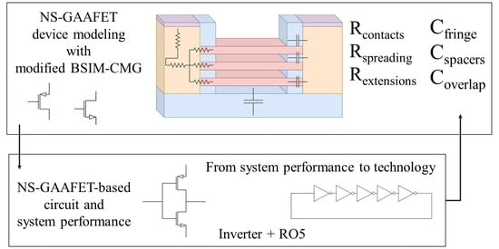
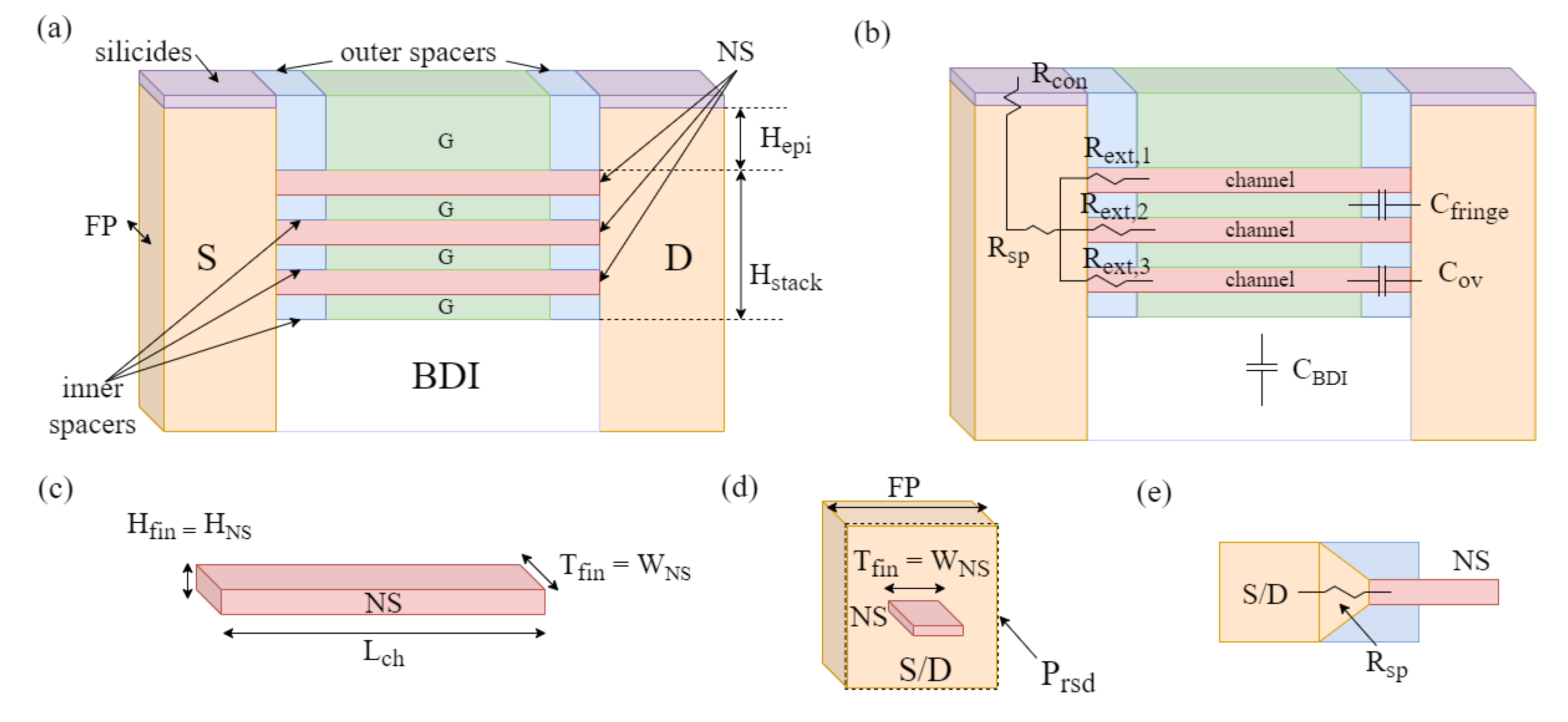
2. Model
3. Model Equations
4. Methodology, Figures of Merit, and Characterization
- Drain-Induced Barrier Lowering (DIBL): We calculate this from its definition aswhere is the supply voltage, is a low voltage value that we fix to 50 mV, and is the obtained threshold voltage with the voltage , where . We calculate through the second-order derivative of the transcharacteristic, i.e., the maximum transconductance method [22,23].
- Subthreshold Slope (SS): This is defined asFor simplicity, we calulate it as , where indicates an interval (i.e., a difference), and considering an excursion of one decade.
- : Driving ON current, obtained with ;
- : subthreshold leakage OFF current, obtained with and = 0 V;
- ratio.
5. Design, Simulations, and Results
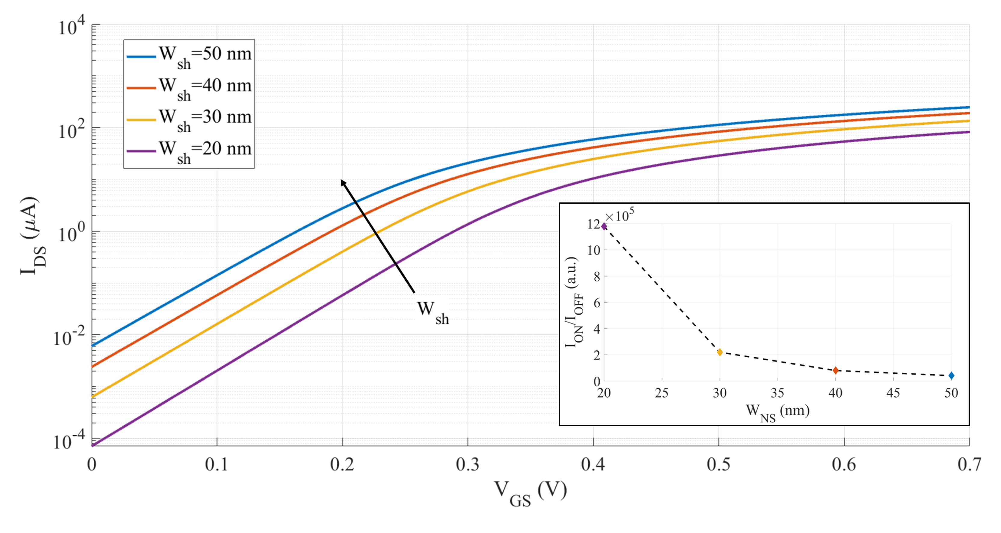
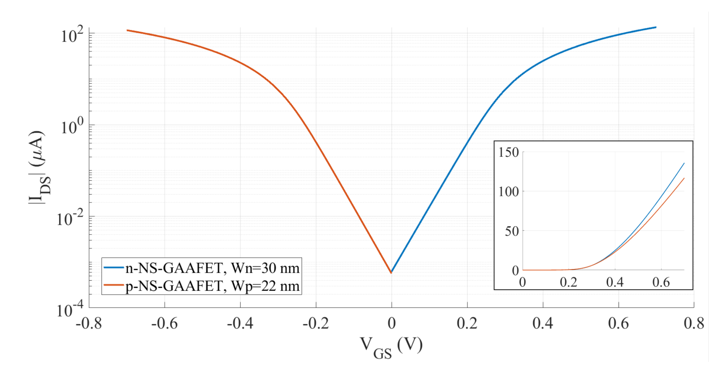
5.1. n-Type NS-GAAFET
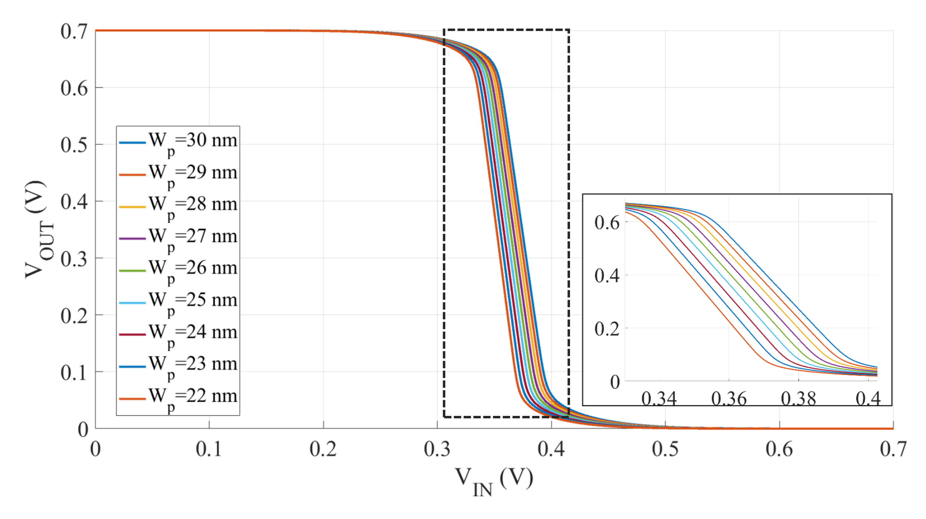
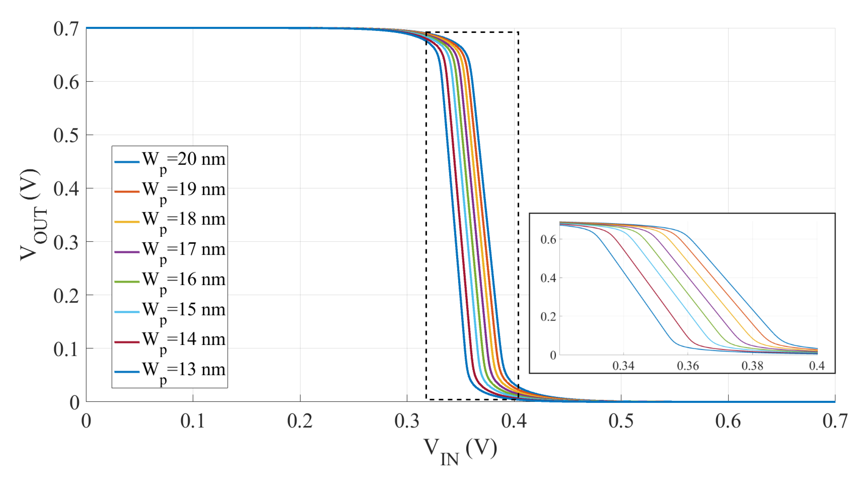
5.2. Digital Inverter
5.2.1. HP Node
5.2.2. LP Node
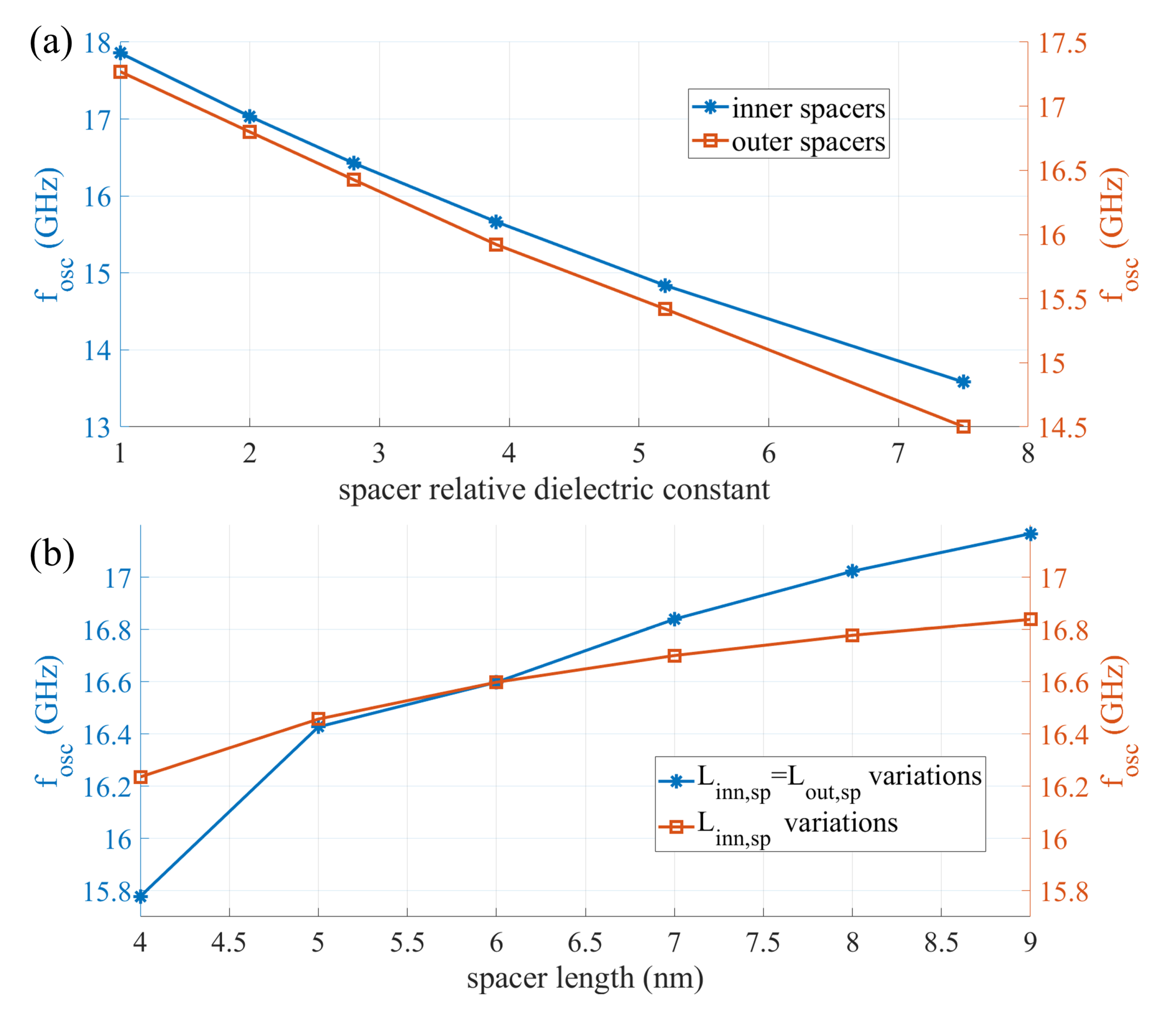
5.3. Five-Stage Ring Oscillator
5.3.1. LP Node ( = 20 nm)
5.3.2. HP Node and Comparison with LP Node
6. Conclusions
Author Contributions
Funding
Data Availability Statement
Conflicts of Interest
References
- Taur, Y.; Ning, T.H. Fundamentals of Modern VLSI Devices, 3rd ed.; Cambridge University Press: Cambridge, UK, 2021. [Google Scholar] [CrossRef]
- Colinge, J. FinFETs and Other Multi-Gate Transistors, 1st ed.; Springer: New York, NY, USA, 2007. [Google Scholar] [CrossRef]
- Saha, S. FinFET Devices for VLSI Circuits and Systems, 1st ed.; CRC Press: Boca Raton, FL, USA, 2020. [Google Scholar] [CrossRef]
- Vacca, M.; Turvani, G.; Riente, F.; Graziano, M.; Demarchi, D.; Piccinini, G. TAMTAMS: An open tool to understand nanoelectronics. In Proceedings of the 2012 12th IEEE International Conference on Nanotechnology (IEEE-NANO), Birmingham, UK, 20–23 August 2012; pp. 1–5. [Google Scholar] [CrossRef]
- Kwon, U.; Park, Y.; Kim, Y.S.; Yoo, J.; Kim, D.S. TCAD challenges and opportunities to find a feasible device architecture for sub-3 nm scaling. In Proceedings of the 2021 International Conference on Simulation of Semiconductor Processes and Devices (SISPAD), Dallas, TX, USA, 27–29 September 2021; pp. 5–10. [Google Scholar] [CrossRef]
- Yoon, J.S.; Jeong, J.; Lee, S.; Lee, J.; Lee, S.; Baek, R.H.; Lim, S.K. Performance, Power, and Area of Standard Cells in Sub 3 nm Node Using Buried Power Rail. IEEE Trans. Electron Devices 2022, 69, 894–899. [Google Scholar] [CrossRef]
- Linten, D.; Hellings, G.; Chen, S.H.; Groeseneken, G. ESD in FinFET technologies: Past learning and emerging challenges. In Proceedings of the 2013 IEEE International Reliability Physics Symposium (IRPS), Monterey, CA, USA, 14–18 April 2013; pp. 2B.5.1–2B.5.8. [Google Scholar] [CrossRef]
- Riente, F.; Hussain, I.; Ruo Roch, M.; Vacca, M. Understanding CMOS Technology Through TAMTAMS Web. IEEE Trans. Emerg. Top. Comput. 2016, 4, 392–403. [Google Scholar] [CrossRef] [Green Version]
- Barraud, S.; Lapras, V.; Previtali, B.; Samson, M.P.; Lacord, J.; Martinie, S.; Jaud, M.A.; Athanasiou, S.; Triozon, F.; Rozeau, O.; et al. Performance and design considerations for gate-all-around stacked-NanoWires FETs. In Proceedings of the 2017 IEEE International Electron Devices Meeting (IEDM), San Francisco, CA, USA, 2–6 December 2017; pp. 29.2.1–29.2.4. [Google Scholar] [CrossRef] [Green Version]
- Bae, G.; Bae, D.I.; Kang, M.; Hwang, S.; Kim, S.; Seo, B.; Kwon, T.; Lee, T.; Moon, C.; Choi, Y.; et al. 3nm GAA Technology featuring Multi-Bridge-Channel FET for Low Power and High Performance Applications. In Proceedings of the 2018 IEEE International Electron Devices Meeting (IEDM), San Francisco, CA, USA, 1–5 December 2018; pp. 28.7.1–28.7.4. [Google Scholar] [CrossRef]
- IEEE International Roadmap for Devices and Systems, 2021 Edition — Executive Report. Available online: https://irds.ieee.org/ (accessed on 28 January 2023).
- Zhang, J.; Frougier, J.; Greene, A.; Miao, X.; Yu, L.; Vega, R.; Montanini, P.; Durfee, C.; Gaul, A.; Pancharatnam, S.; et al. Full Bottom Dielectric Isolation to Enable Stacked Nanosheet Transistor for Low Power and High Performance Applications. In Proceedings of the 2019 IEEE International Electron Devices Meeting (IEDM), San Francisco, CA, USA, 7–11 December 2019; pp. 11.6.1–11.6.4. [Google Scholar] [CrossRef]
- Li, J.; Li, Y.; Zhou, N.; Xiong, W.; Wang, G.; Zhang, Q.; Du, A.; Gao, J.; Kong, Z.; Lin, H.; et al. Study of Silicon Nitride Inner Spacer Formation in Process of Gate-all-around Nano-Transistors. Nanomaterials 2020, 10, 793. [Google Scholar] [CrossRef] [PubMed]
- Shen, T.; Watanabe, K.; Zhou, H.; Belyansky, M.; Stuckert, E.; Zhang, J.; Greene, A.; Basker, V.; Wang, M. A new technique for evaluating stacked nanosheet inner spacer TDDB reliability. In Proceedings of the 2020 IEEE International Reliability Physics Symposium (IRPS), Dallas, TX, USA, 28 April–30 May 2020; pp. 1–5. [Google Scholar] [CrossRef]
- Yakimets, D.; Bardon, M.G.; Jang, D.; Schuddinck, P.; Sherazi, Y.; Weckx, P.; Miyaguchi, K.; Parvais, B.; Raghavan, P.; Spessot, A.; et al. Power aware FinFET and lateral nanosheet FET targeting for 3nm CMOS technology. In Proceedings of the 2017 IEEE International Electron Devices Meeting (IEDM), San Francisco, CA, USA, 2–6 December 2017; pp. 20.4.1–20.4.4. [Google Scholar] [CrossRef]
- Paydavosi, N.; Venugopalan, S.; Chauhan, Y.S.; Duarte, J.P.; Jandhyala, S.; Niknejad, A.M.; Hu, C.C. BSIM—SPICE Models Enable FinFET and UTB IC Designs. IEEE Access 2013, 1, 201–215. [Google Scholar] [CrossRef]
- Volksen, W.; Miller, R.D.; Dubois, G. Low Dielectric Constant Materials. Chem. Rev. 2010, 110, 56–110. [Google Scholar] [CrossRef] [PubMed]
- Gu, M.; Wang, X.; Li, W.; Aquilino, M.; Peng, J.; Wang, H.; Jaeger, D.; Tabakman, K.; Carter, R.; Hu, O.; et al. Hybrid low-k spacer scheme for advanced FinFET technology parasitic capacitance reduction. Electron. Lett. 2020, 56, 514–516. [Google Scholar] [CrossRef]
- Wang, Y.; Kumar, R. Stability of Carbon-Doped Silicon Oxide Low-k Thin Films. J. Electrochem. Soc. 2004, 151, F73. [Google Scholar] [CrossRef]
- Rabaey, J.; Chandrakasan, A.; Nikolic, B. Digital Integrated Circuits: A Design Perspective. Electronics and VLSI Series, 2nd ed.; Pearson Education: London, UK, 24 December 2002. [Google Scholar]
- Ribas, R.P.; Reis, A.I.; Ivanov, A. Performance and functional test of flip-flops using ring oscillator structure. In Proceedings of the 2011 IEEE 6th International Design and Test Workshop (IDT), Beirut, Lebanon, 11–14 December 2011; pp. 42–47. [Google Scholar] [CrossRef]
- Ortiz-Conde, A.; García Sánchez, F.; Liou, J.; Cerdeira, A.; Estrada, M.; Yue, Y. A review of recent MOSFET threshold voltage extraction methods. Microelectron. Reliab. 2002, 42, 583–596. [Google Scholar] [CrossRef]
- Rudenko, T.; Kilchytska, V.; Md A, M.K.; Raskin, J.P.; Nazarov, A.; Flandre, D. On the MOSFET Threshold Voltage Extraction by Transconductance and Transconductance-to-Current Ratio Change Methods: Part II—Effect of Drain Voltage. IEEE Trans. Electron Devices 2012, 58, 4180–4188. [Google Scholar] [CrossRef]
- Na, M.; Nowak, E.; Haensch, W.; Cai, J. The effective drive current in CMOS inverters. In Proceedings of the Digest. International Electron Devices Meeting, San Francisco, CA, USA, 8–11 December 2002; pp. 121–124. [Google Scholar] [CrossRef]
- Hu, J.; Park, J.E.; Freeman, G.; Wachnik, R.; Wong, H.S.P. Effective Drive Current in CMOS Inverters for Sub-45nm Technologies. In Proceedings of the NSTI-Nanotech, Boston, MA, USA, 1–5 June 2008; Volume 3. [Google Scholar]


| 3 | 3.2 nm | ||
| 20 nm (HP); 30 nm (LP/Memory) | 25 | ||
| 7 nm | 3.9 | ||
| 14 nm | 3.9 | ||
| FP | 49 nm | cm−3 | |
| 10 nm | cm−3 | ||
| 10 nm | cm−3 |
| Material | Relative Dielectric Constant |
|---|---|
| vacuum (air) | 1 |
| porous SiO2 and/or polymeric materials | 2 |
| carbon-doped oxide | 2.8 |
| SiO2 | 3.9 |
| SiOCN | 5.2 |
| Si3N4 | 7.5 |
| (nm) | 20 | 30 | 40 | 50 |
| DIBL (mV/V) | 12.3 | 30.8 | 43.1 | 52.3 |
| SS (mV/dec) | 67 | 69 | 72 | 73 |
| (a.u.) | 1.18·10 | 2.19·10 | 8.02·10 | 4.12·10 |
| (µA) | 87 | 148 | 202.5 | 263 |
| 20 nm | 19.9% | 24.8% | 20.22% | 10.51% | 2.44% |
| 30 nm | 11.39% | 13.34% | 14.89% | 5.31% | 3.83% |
Disclaimer/Publisher’s Note: The statements, opinions and data contained in all publications are solely those of the individual author(s) and contributor(s) and not of MDPI and/or the editor(s). MDPI and/or the editor(s) disclaim responsibility for any injury to people or property resulting from any ideas, methods, instructions or products referred to in the content. |
© 2023 by the authors. Licensee MDPI, Basel, Switzerland. This article is an open access article distributed under the terms and conditions of the Creative Commons Attribution (CC BY) license (https://creativecommons.org/licenses/by/4.0/).
Share and Cite
Mo, F.; Spano, C.E.; Ardesi, Y.; Ruo Roch, M.; Piccinini, G.; Vacca, M. NS-GAAFET Compact Modeling: Technological Challenges in Sub-3-nm Circuit Performance. Electronics 2023, 12, 1487. https://doi.org/10.3390/electronics12061487
Mo F, Spano CE, Ardesi Y, Ruo Roch M, Piccinini G, Vacca M. NS-GAAFET Compact Modeling: Technological Challenges in Sub-3-nm Circuit Performance. Electronics. 2023; 12(6):1487. https://doi.org/10.3390/electronics12061487
Chicago/Turabian StyleMo, Fabrizio, Chiara Elfi Spano, Yuri Ardesi, Massimo Ruo Roch, Gianluca Piccinini, and Marco Vacca. 2023. "NS-GAAFET Compact Modeling: Technological Challenges in Sub-3-nm Circuit Performance" Electronics 12, no. 6: 1487. https://doi.org/10.3390/electronics12061487