All articles published by MDPI are made immediately available worldwide under an open access license. No special
permission is required to reuse all or part of the article published by MDPI, including figures and tables. For
articles published under an open access Creative Common CC BY license, any part of the article may be reused without
permission provided that the original article is clearly cited. For more information, please refer to
https://www.mdpi.com/openaccess.
Feature papers represent the most advanced research with significant potential for high impact in the field. A Feature
Paper should be a substantial original Article that involves several techniques or approaches, provides an outlook for
future research directions and describes possible research applications.
Feature papers are submitted upon individual invitation or recommendation by the scientific editors and must receive
positive feedback from the reviewers.
Editor’s Choice articles are based on recommendations by the scientific editors of MDPI journals from around the world.
Editors select a small number of articles recently published in the journal that they believe will be particularly
interesting to readers, or important in the respective research area. The aim is to provide a snapshot of some of the
most exciting work published in the various research areas of the journal.
Department of Electrical Engineering, Federal University of Espírito Santo (UFES), Av. Fernando Ferrari, Vitória 29075-910, Brazil
2
Department of Applied Mathematics, Materials Science and Engineering and Electronic Technology, Superior School of Experimental Sciences and Technology-ESCET, University Rey Juan Carlos, 28933 Madrid, Spain
*
Author to whom correspondence should be addressed.
This research paper studies and highlights the features of the most popular finite control set model predictive control (FCS-MPC) strategies available in the state of the art, which are the optimal switching vector (OSV-MPC), modulated model predictive control (M2PC), and optimal switching sequence (OSS-MPC) methods. Thus, these strategies are studied experimentally by analyzing the transient and steady state performance using a grid tie conventional three-phase two-level voltage source inverter (VSI) with inductive output filter in a Typhoon HIL real-time simulator (RTS) with a Texas Instruments F28379D digital signal processor (DSP). Hence, quantitative indicators, such as the maximum tracking error, the mean absolute error, the settling time, the total harmonic distortion, the switching frequency spectrum, the switching pattern, and the computational burden are compared with the aim to deduce the best strategy for each criteria.
To provide the electrical power required by the electrical loads, it is necessary to use electrical power converters which also used to enhance the electrical power efficiency. In fact, this is necessary for many applications such as electrical vehicles and distributed generation, which require a continuous enhancement in the technology used. Indeed, the control of the power converters is considered one of the important points of interest in the power electronics field. Initially, this step was performed using operational amplifiers. Then, digital signal processors (DSPs) were introduced to generate the control signals for the switches [1,2]. These technologies allowed the use of intelligent control techniques, namely, fuzzy logic, sliding mode, artificial neural network (ANN), and predictive control [1,2,3,4,5].
For instance, predictive control uses the system model and prediction to generate the signals control [1,4,5]. Among various predictive control techniques, model predictive control (MPC) is used in power converter applications [2,3,4,6]. Indeed, MPC consists in predicting the values of variables to be controlled. To do so, a cost function is used and minimized in such a way that the optimum value of the control signals of the power converter switching states are calculated at each sample time [4,6,7]. Based on the type of optimization (integer or non-integer), two subdivisions may be considered for the MPC. The first one consists in the non-integer optimization MPC, known as the continuous control set (CCS-MPC) which uses continuous signals to control the converter. The implementation of CCS-MPC is characterized by its high complexity [5,6]. However, lower computational cost, fixed switching frequency, and the possibility to expand the prediction horizon are the main advantages of CCS-MPC [6]. The second subdivision is the integer MPC optimization technique, known as the finite control set (FCS-MPC) [5,6,7], which utilizes the discrete nature of power converters, with finite switching states for the control of the converter switches. In fact, FCS-MPC does not require a modulator and control algorithm [3,5,6]. Indeed, this technique is considered as the most useful for the power converters control [5,6], despite its significant computational cost. This is noticed especially in the case of long prediction horizon in which the optimization is online and it considers many possibilities in the optimization procedure on every sampling time [6,7]. Moreover, FCS-MPC can be classified on the optimal switching vector (OSV-MPC) and optimal switching sequence (OSS-MPC) based on the applied switching vector application [6]. For instance, OSV-MPC is a very popular MPC technique that uses all available switching vectors as possible control actions on the converter. In fact, a cost function that includes all the possible switching vectors is used. Hence, the vector that fulfills the lowest cost function is applied to the converter during the switching period [6]. This cost function is minimized in such a way that the same vector can be applied to the converter for the next switching selection. Hence, a variable switching frequency limited to can be obtained. Moreover, the average value of is usually much lower than this value [8]. In addition, generates a spread frequency spectrum at the output of the converter. This means that higher complexity in filter design is obtained, on the one hand, and an inferior harmonic response with higher total harmonic distortion (THD) is generated, on the other hand, which is considered one of the most significant drawbacks of this technique [6,8].
To overcome this OSV-MPC issue, many solutions have been analyzed in the literature. For example, a hybrid OSV-MPC is studied in [9], in which the optimized control signals are filtered using a low-pass filter before being applied to a pulse width modulator (PWM). This method demonstrated a better frequency spectrum owing to the use of the filter and a modulator in the control design. Moreover, in the research paper [10], the authors used the virtual state vector to archive a constant switching frequency. In fact, this method requires many virtual vectors to be evaluated at low sampling frequencies in such a way that the computational burden can be high to maintain the performance. Other solutions to the frequency problem consist in the modifications of the cost function [11,12,13,14,15]. Indeed, this solution achieves a better frequency spectrum at the cost of the complexity of the cost functions. Therefore although solutions exist, each one has disadvantages and does not adequately solve the problem.
In recent years, OSS-MPC has emerged as a new technique of FCS-MPC in which a set of switching sequences are evaluated at each sample time to generate a cost function. The sequence with the lowest cost functions is selected and applied to the power converter. Thus, the time is introduced as an additional variable and the switching frequency is generated as the set of switching sequences [6]. This allows OSS-MCP to have a higher computational burden when compared with OSV-MPC [6].
Another FCS-MPC technique that has been widely used is modulated model predictive control (M2PC). In fact, the technique uses a modulator as part of the cost function elaboration that produces a constant switching frequency [6]. M2PC has a computational burden lower than OSS-MPC and is characterized by a simpler implementation process.
As FCS-MPC is considered an advantageous technique to control power converters, this research paper presents an extend comparison between OSV-MPC, M2PC, and OSS-MPC applied to the grid tie conventional three-phase two-level voltage source inverter (VSI) with an inductive output filter. All the three techniques are described in detail. Moreover, an experimental comparison in steady and transient states is conducted to evaluate each technique. The experiments are implemented using a Typhoon HIL 402 real-time simulator (RTS) with a Texas Instruments F28379D digital signal processor (DSP). A previous FCS-MPC comparison paper [16] compared four different techniques; however, it did not compare the most recent one, which is the OSS-MPC. Another comparison research paper [17] studied the same three techniques of this research paper. However, both papers only presented Matlab®/Simulink simulation results. Therefore, they did not addressed the computational delay problem since they only presented the physical controllers’ implementation. As far as other research, a methodology to compensate the computational delay for M2PC was not found. Thus, to overcome this issue, the present research work studies an OSS-MPC based on delay compensation.
This research paper is structured as follows: Section 2 describes the three-phase two-level VSI connected to the electrical grid and the power converter selected for the implementation. The in-depth description of the three FCS-MPC techniques and their applications to power converters are presented in Section 3, Section 4 and Section 5. Section 6 presents the experimental setup and the results related with the stead state and transient conditions. The paper ends with a conclusion presented in Section 7.
2. Two-Level Voltage Source Inverter
The three-phase two-level VSI is one of the most used power converters owing to its simple topology and its capacity to operate with bidirectional power flow. In fact, several applications of VSI have been studied in literature such as uninterruptible power supplies (UPS), adjustable-speed drives, battery management systems (BMS), static synchronous compensators (STATCOM), active power filters, and grid-tie converters [18].
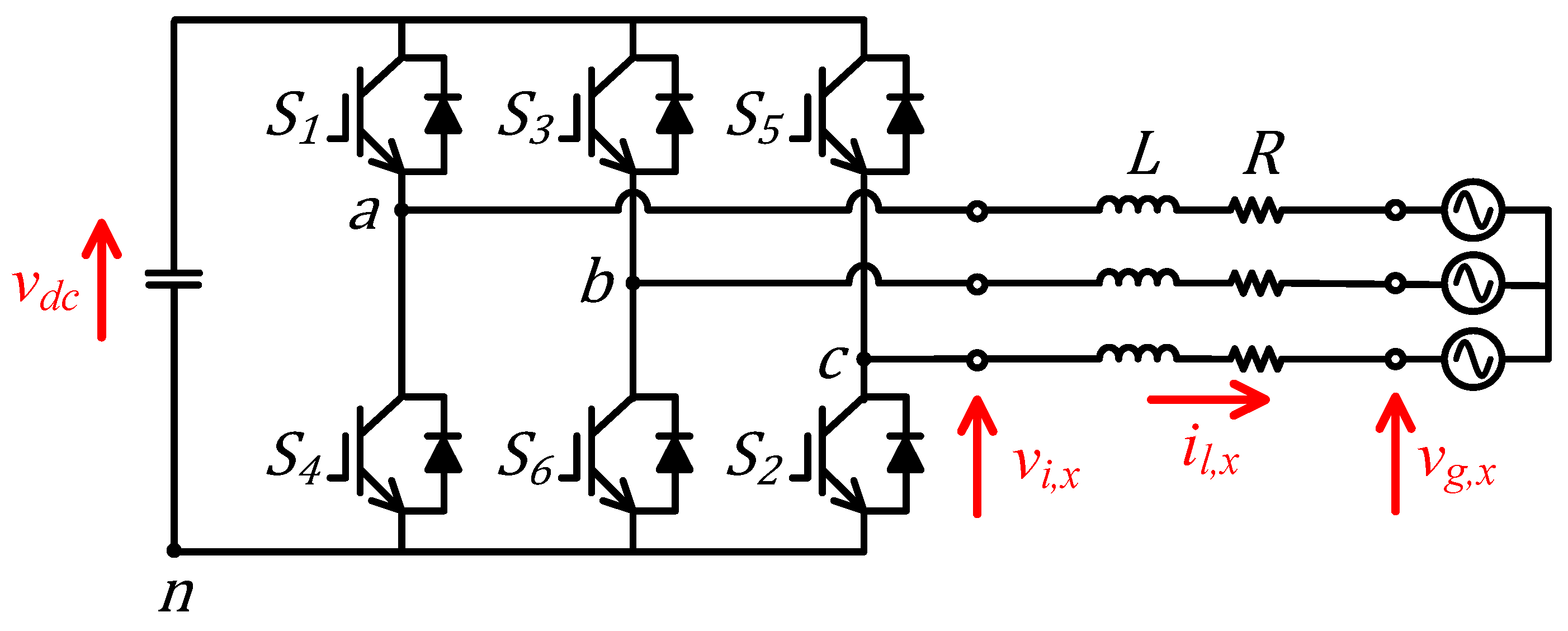
In this research paper, the three-phase two-level VSI is considered. Indeed, it is connected to the electrical grid through an inductor filter with internal resistance . This configuration could represent a photovoltaic generation system connected to the grid. The schematic diagram of the converter connected to the grid is shown in Figure 1.
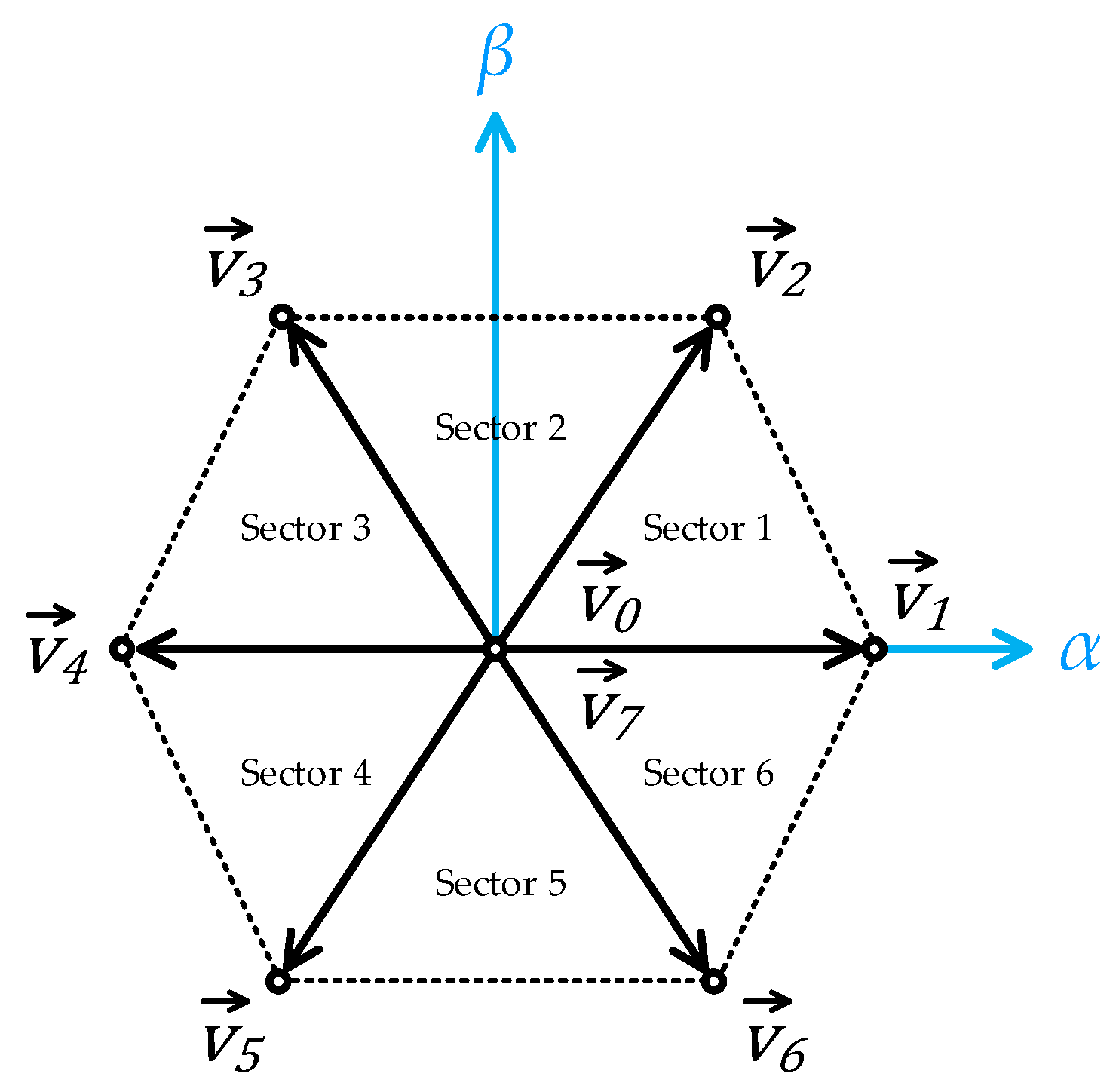
The three-phase two-level VSI presents eight possible switching states for the power switches S1 to S6. In fact, the same leg switches of the converter are driven in a complementary manner to avoid short circuits in the DC voltage source. The possible switching states for the upper, and consequently for the lower, switches , , and are presented in Table 1 [19]. Applying Equation (1), which represents the invariable amplitude Clarke transformation [20], the eight possible switching states can be represented as eight space vectors in the -axis.
Table 1 also presents the calculated space vectors.
The vectors presented in Table 1 generate 6 sectors in the -axis which are shown in Figure 2. The converter presented in Figure 1 is used as a four quadrants power source for the electrical grid, having as references the active power P * and the reactive power Q *. The use of the inductive filter output is necessary to allow the electrical power to be exchanged and the output current harmonic content to be reduced.
2.1. System Modeling
The system modeling in the -axis can be obtained directly from Kirchhoff’s laws in the circuit formed by the inverter and the electrical grid (Figure 1). The equations obtained in the -axis are converted to the -axis using Clarke transformation to reduce the number of equations and the computational burden of the three MPC algorithms implemented [21].
2.1.1. Inductor Current Gradient
The inductor current gradient of the grid-tie two-level VSI with an output L filter in the -axis is described by Equation (2).
The invariable amplitude Clarke transformation [20] is presented in Equation (3) and is used to convert the Equation (2) -axis into the -axis as shown in Equation (4); the circuit is considered balanced with a null zero-sequence component.
2.1.2. Inductor Current Discretization
To implement the FCS-MPC strategies, Equation (4) must be discretized. Thus, the Euler forward method is used here since it is characterized by its satisfactory approximation for first-order systems. Moreover, for higher-order systems, the error becomes relevant, and an exact discretization method must be used [1]. Equation (5) presents the Euler forward method for the derivative approximation.
Using the approximation presented in Equation (5) in Equation (4) generates the discretized equations for the converter. The discretized equations are shown in Equation (6).
2.1.3. Current Reference
To control the controller’s power exchange with the grid, the P * and Q * references are used with voltage measurements to generate the current references which are applied in the FCS-MPC control. From the instantaneous power theory in the -axis, the references are calculated as shown in Equation (7) [20].
2.2. Space Vector Modulation Switching Pattern
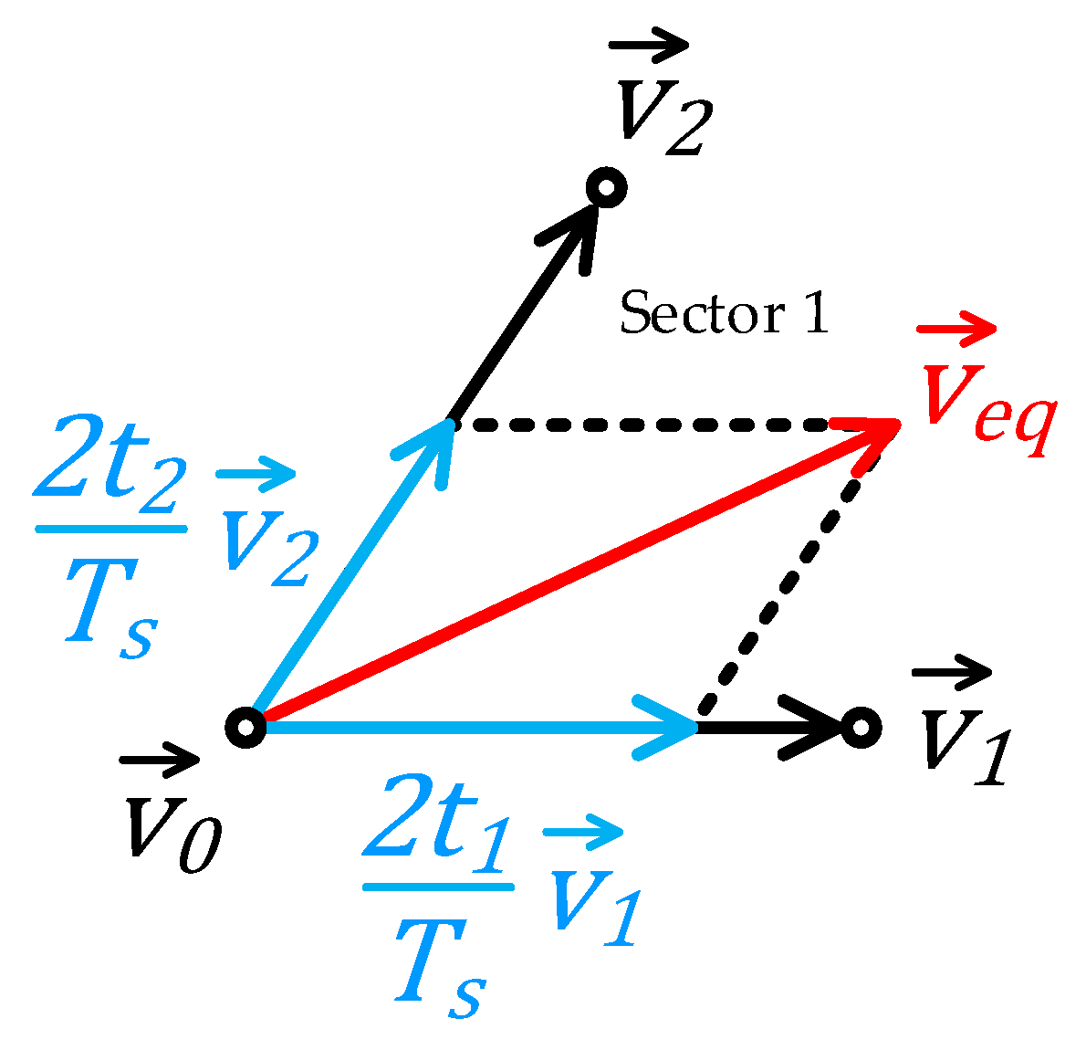
Space vector modulation (SVM) is a popular modulation method used for three-phase two-level VSI. In fact, compared with the sinusoidal pulse width modulation, SVM has the enhanced application of the DC voltage link and reduced THD [19]. Indeed, the technique consists in synthetizing a desired equivalent voltage vector composed of two actives and one zero based on three stationary vectors. Hence, the vectors in the plane (Figure 2) can be generated by choosing the two adjacent vectors and the application times. Considering a sufficiently reduced sample time , the equivalent vector can be approximated as shown in Equation (8). Figure 3 shows the construction that corresponds to the first sector.
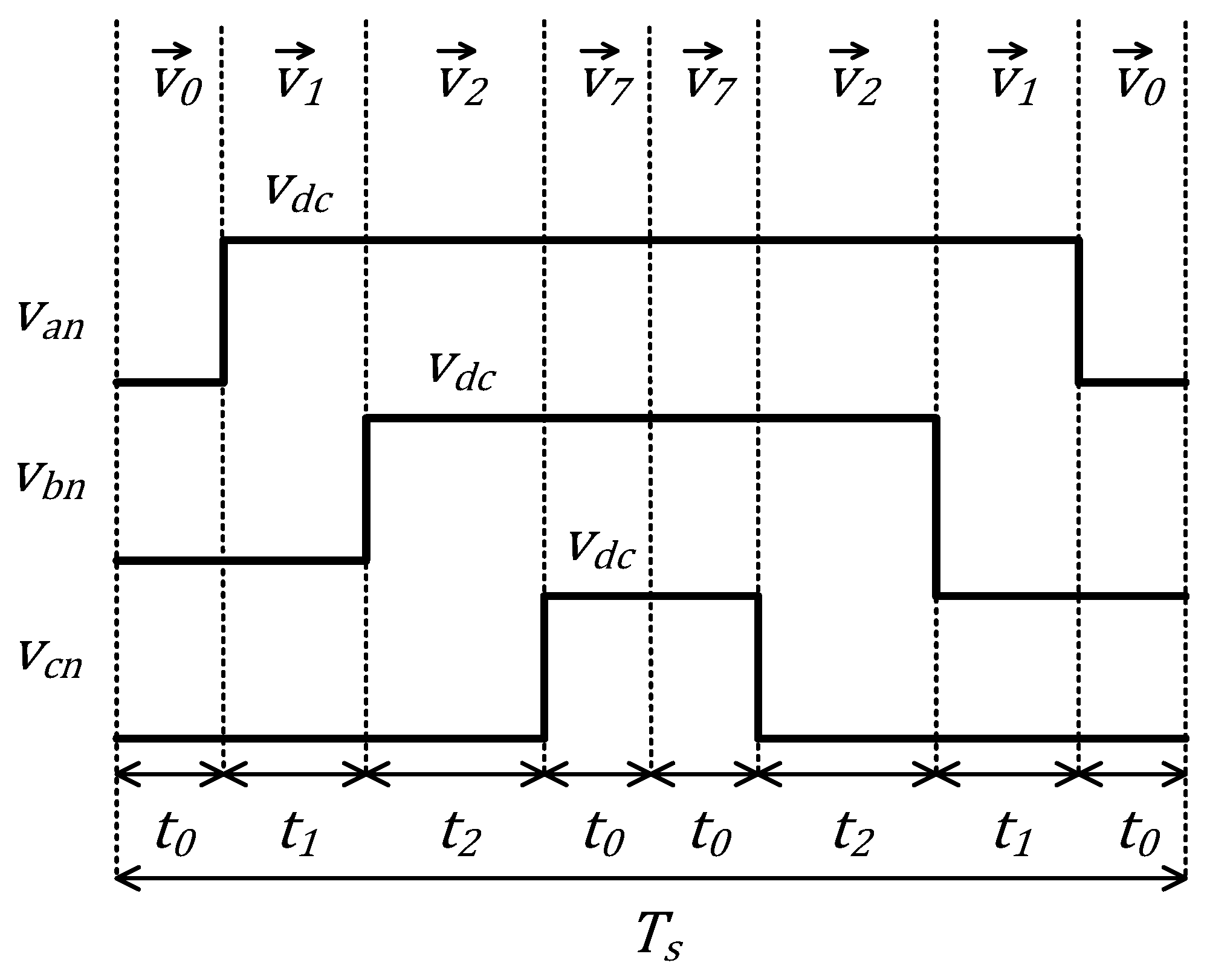
The SVM modulation has a defined way to calculate the application times, , , and , that depends on the voltage that should be generated [22]. In fact, the SVM principle is applied for the implementation of M2PC and OSS-MPC control techniques that generate vectors for the control of the converter switches. Indeed, the switching sequence is a 7-segment type generated at a fixed switching frequency which is equal to the sampling frequency [22]. Figure 4 illustrates the seven-segment switching sequence that corresponds to sector one. Moreover, in Table 2, the vector sequence and its application times for the six sectors is described.
Owing to the seven-segment switching advantages, in this research paper, the control techniques M2PC and OSS-MPC developed are implemented using this switching sequence.
3. OSV-MPC
The OSV-MPC operation implementation in power converters is simple since it consists of producing a finite number of possible switching states that are combined with the converter discrete model to predict the future value of the vector variables that minimizes a cost function during the sample time [23].
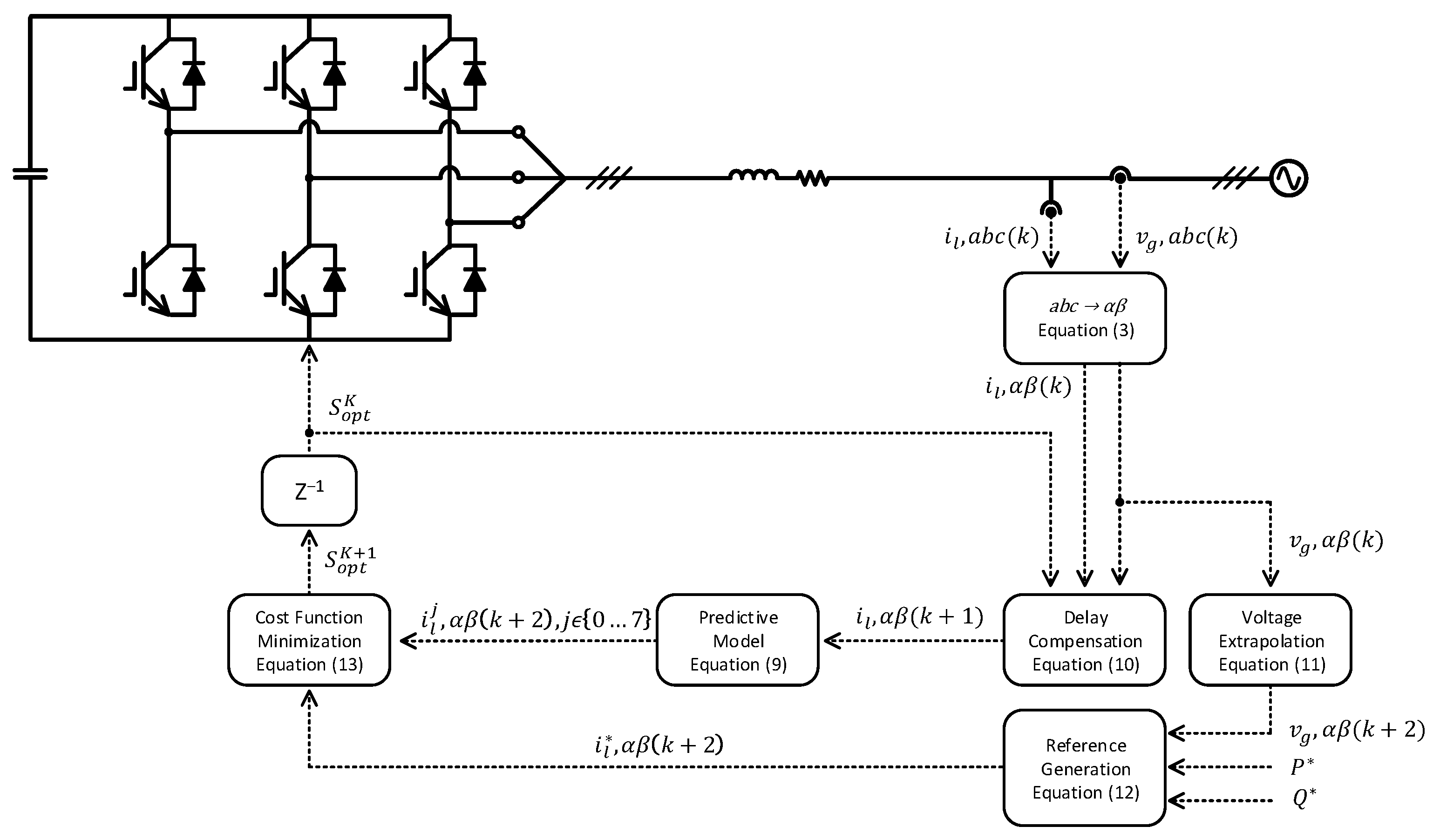
Based on the evaluation of the possible switching states and compared with the classical control techniques, the computational performance of the OSV-MPC algorithm is higher [24]. In fact, the delay between measurements and the switching of the converter can be critical and may reduce the efficiency of the control response [24]. Therefore, in this case, it is necessary to use a delay compensation [24] which is based on applying a prediction. The OSV-MPC algorithm steps with delay compensation for the converter studied in this research paper are shown below. In Figure 5, the block diagram of the converter with the OSV-MPC control is presented.
3.1. Predictive Model and Delay Compensation
In the three-phase two-level VSI with the OSV-MPC control, the inductor current and grid voltage are measured (Figure 5). In this method, Equation (3) is applied to convert to the -axis and then the switching vector evaluated in the previous sample period is applied to the switches of the converter, thus guaranteeing no interference in the switching. Since the three-phase two-level VSI includes eight possible switching vectors, therefore the converter has eight possible predictive inductor currents which can be deduced by applying Equation (9), where represents the eight possible voltages generated by the inverter and represents the current predictions as described below:
Then, the current value is calculated from the present switching vector and measurements by applying Equation (6). Finally, the delay compensation for the inductor current can be obtained using Equation (10).
3.2. Reference Generation
The current references used in the cost functions are obtained from the power references and the use of Equation (7) by performing the calculation of to avoid the delays. The implementation of the compensation is conducted by extrapolating the measured voltages to k + 2. For example, the authors of [1] applied two extrapolation techniques for this purpose. The first one consists in the use of the order 2 Lagrange extrapolation formula. The second method for extrapolation consists in the vector angle compensation, which is the method that will be used in this research paper. In fact, this method considers the estimated changes in the vector angle during a sample time considering a sinusoidal signal. The reference extrapolation formula used to compensate the measured grid voltage is described in Equation (11):
where is the grid frequency.
The reference currents are obtained from the power references using Equation (12).
3.3. Cost Function Minimization
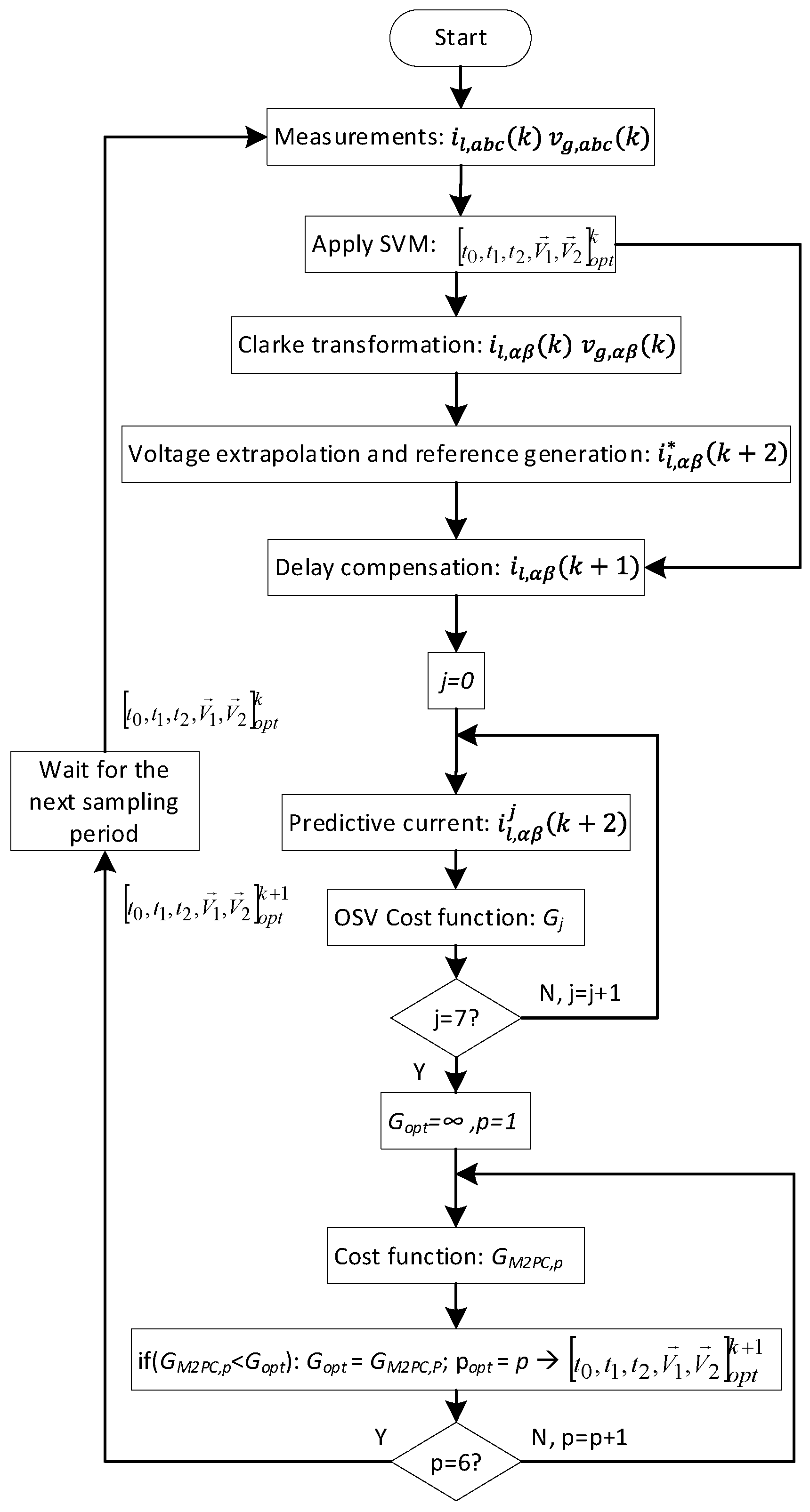
The minimization of the cost function is to obtain the switching vector index that minimizes the current error. In fact, it is evaluated for all the eight possible vectors and deduced in such a way that a global optimal solution that corresponds to an optimum vector index and switching vector are obtained. Thus, the is applied to the switches of the converter in the next , so the computational delay is avoided. Equation (13) describes how the cost function is minimized and Figure 6 illustrates the flowchart of the developed OSV-MPC controller.
4. M2PC-MPC
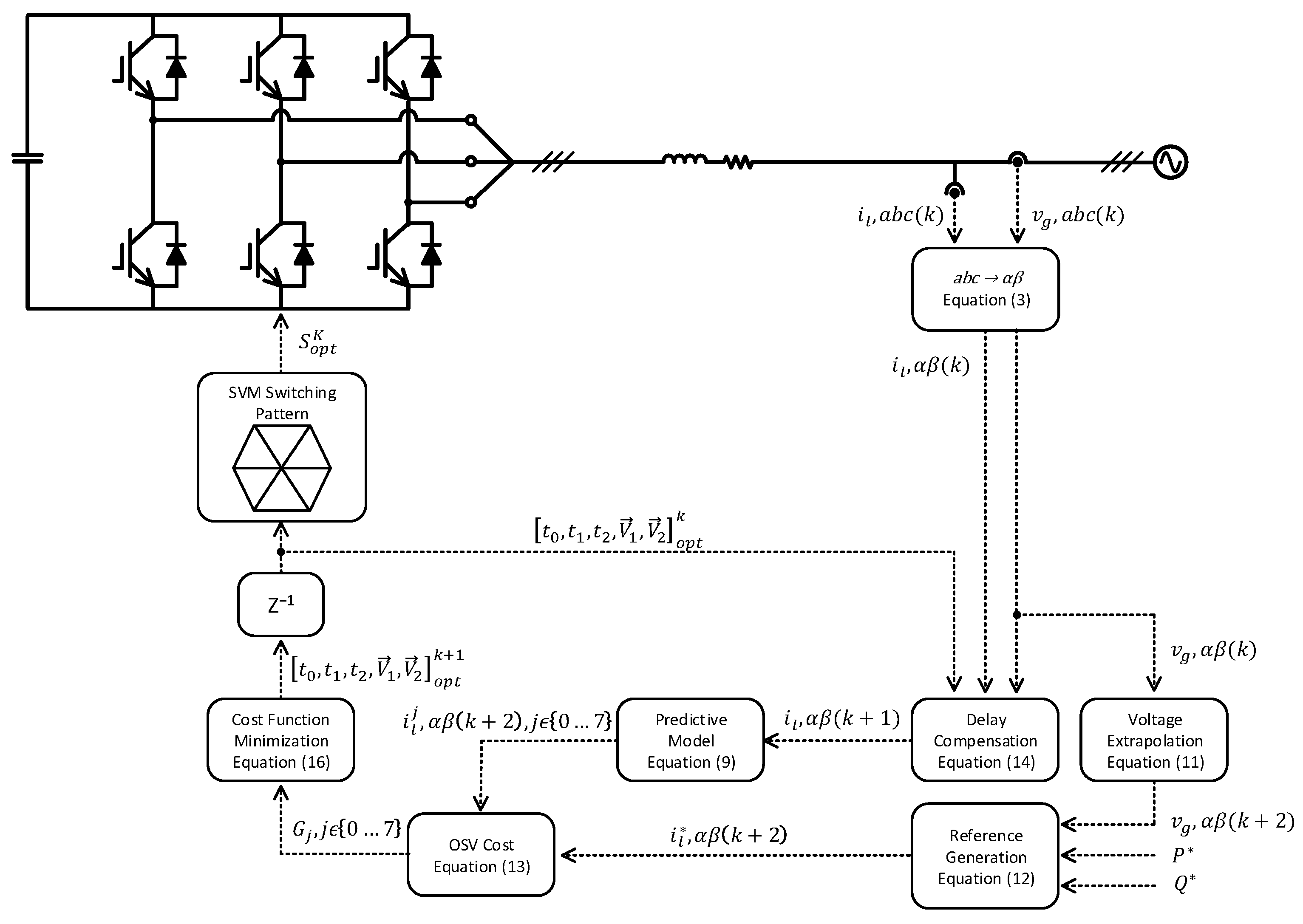
The M2PC technique applied to the three-phase two level VSI incorporates the classical SVM modulation as part of the FCS-MPC optimization procedure [25,26]. In fact, the discrete model of the system is used to predict the future values of the variables by the calculation of the OSV-MPC cost. Therefore, the optimum sector and vector are deduced for the next step time .
Moreover, M2PC has a higher computational effort when compared with OSV-MPC since the cost function calculated by applying the OSV-MPC should be evaluated in M2PC before the sector optimization. The major advantage between M2PC and OSV-MPC is that the former generates a constant switching frequency and a well-defined harmonic spectrum. Hence, to compensate for the computational delay, an OSV-MPC delay compensation scheme is developed. Its main difference with M2PC is that an equivalent vector is required as more than one vector is applied at the output at each sample time . Figure 7 describes the block diagram used in this paper to implement the M2PC algorithm with delay compensation.
4.1. Predictive Model and Delay Compensation
The grid voltages and inductor currents are measured and transformed by applying the Clarke transformation method. Thus, the vectors calculated in the previous sample time are applied to the switches using the SVM seven-segment pattern. Then, the predictive model obtained using Equation (6) is applied to calculate the eight possible predictive inductor currents (Equation (9)). Then, the delay compensation is implemented using Equation (9) by calculating the inductor currents at the k + 1 sample time. The difference from OSV-MPC is that for the M2PC, two active vectors and one zero vector need to be used to calculate . However, for OSV-MPC only one vector is required. The delay compensation scheme used for OSS-MPC [27] is extended for M2PC. Considering the switching vectors sequence and application times presented in Table 2, the equivalent predicted current is calculated as:
where the gradients from Equation (4) are used to obtain the current with the optimum application times obtained from the previous sample time. The vectors , which correspond to the optimum vectors of the previous sample time, are applied for the gradient calculations as shown in Equation (15).
4.2. Reference Generation
The current reference and are calculated from Equation (12).
4.3. Cost Function Minimization
An initial vector OSV cost is calculated as described in Equation (13) by performing all the eight possible switching vectors . Then, the next step consists in calculating the cost function that corresponds to the new sector , followed by the vectors and switching times of the converter’s switches. Hence, the new sector cost function is defined using Equation (16), where , , are the sector vectors duty cycles with 0, 1, and 2 null and two active vector indexes.
Considering a constant and assuming that the vector duty cycle is inversely proportional to its cost, the system in Equation (17) is used here to obtain sector vectors duty cycles.
Thus, solving the system presented by Equation (17), the constant and the duty cycles are as follows:
Hence, substituting Equation (18) in Equation (16), the new sector cost function to be minimized is given by Equation (19), which is evaluated for the six sectors of the -axis.
Therefore, the sector that fulfills a minimum cost is selected, and then the vectors and application times are applied in the next using the SVM modulator. Hence, the switching times are issued from the duty cycles as presented in Equation (20). Figure 8 describes the flowchart of the developed M2PC controller.
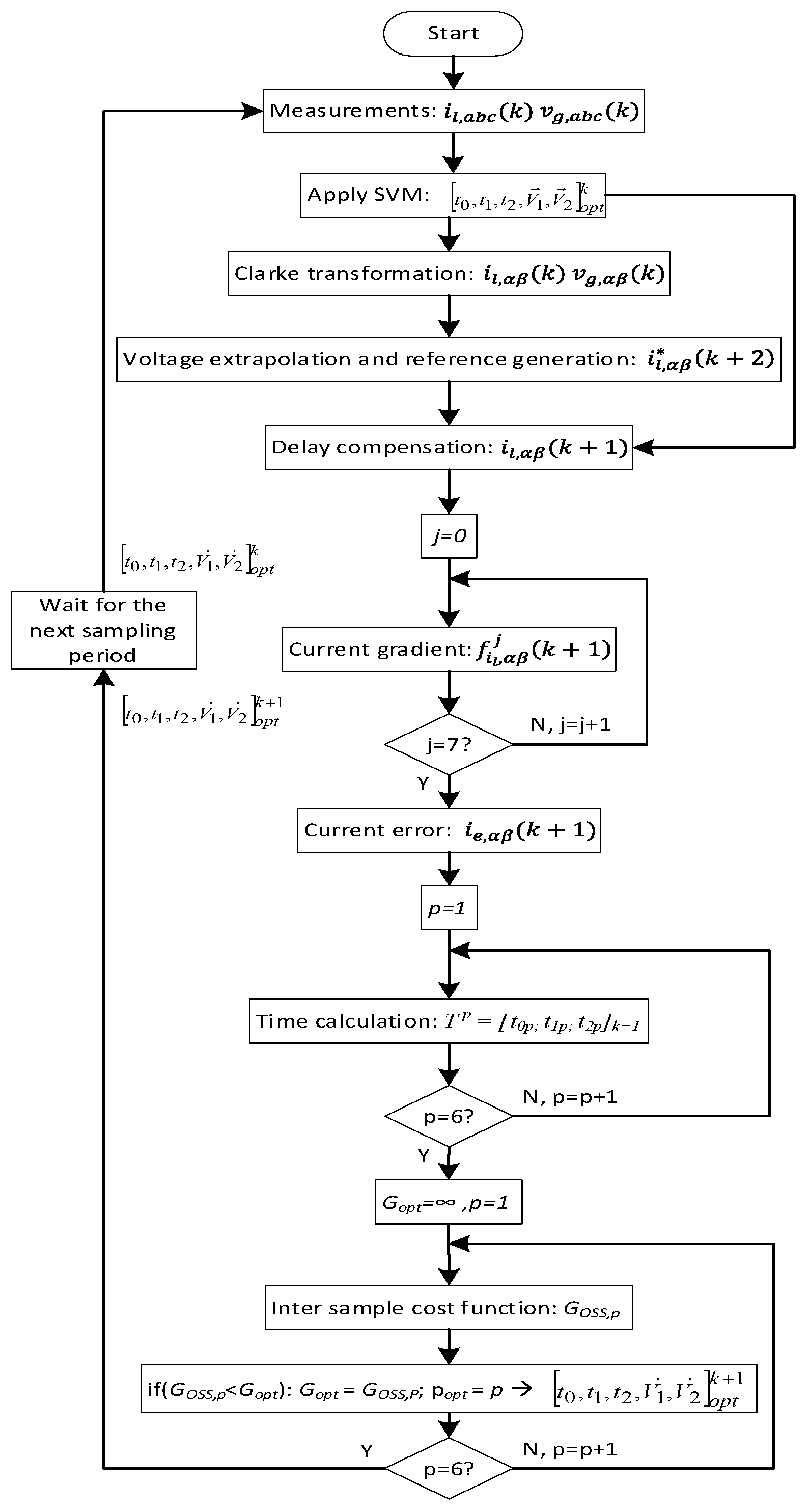
5. OSS-MPC
Among the three FCS-MPC techniques studied in this research paper, OSS-MPC is the most recent technique used for three-phase two-level VSI. For example, in [27,28] the authors described the implementation of the control algorithm. For this, two optimizations’ techniques were implemented. In fact, the first one performs the calculation in an offline way. However, the second one conducts the calculation at each sample time in such a way to minimize the cost function. Thus, owing to its advantages, the switching sequence selected for implementation is the SVM seven-segment switching pattern, as presented in [27] and described in Section 2.2.
The system’s discrete gradients used consist of the equations used to model the system. In fact, the application times and the minimization of the cost function for each sector of the-axis are illustrated in Figure 2. Then, the optimum sector, vectors, and times are applied to the converter using the seven-segment switching pattern in the next . OSS-MPC has the highest computational cost since it allows the vector used for the switch control to be obtained. However, the use of an inter-sample-based cost function improves the steady state response and reduces the output THD when compared with the other techniques [17,27]. This is justified by the fact that the switching frequency is constant owing to the SVM modulation scheme used.
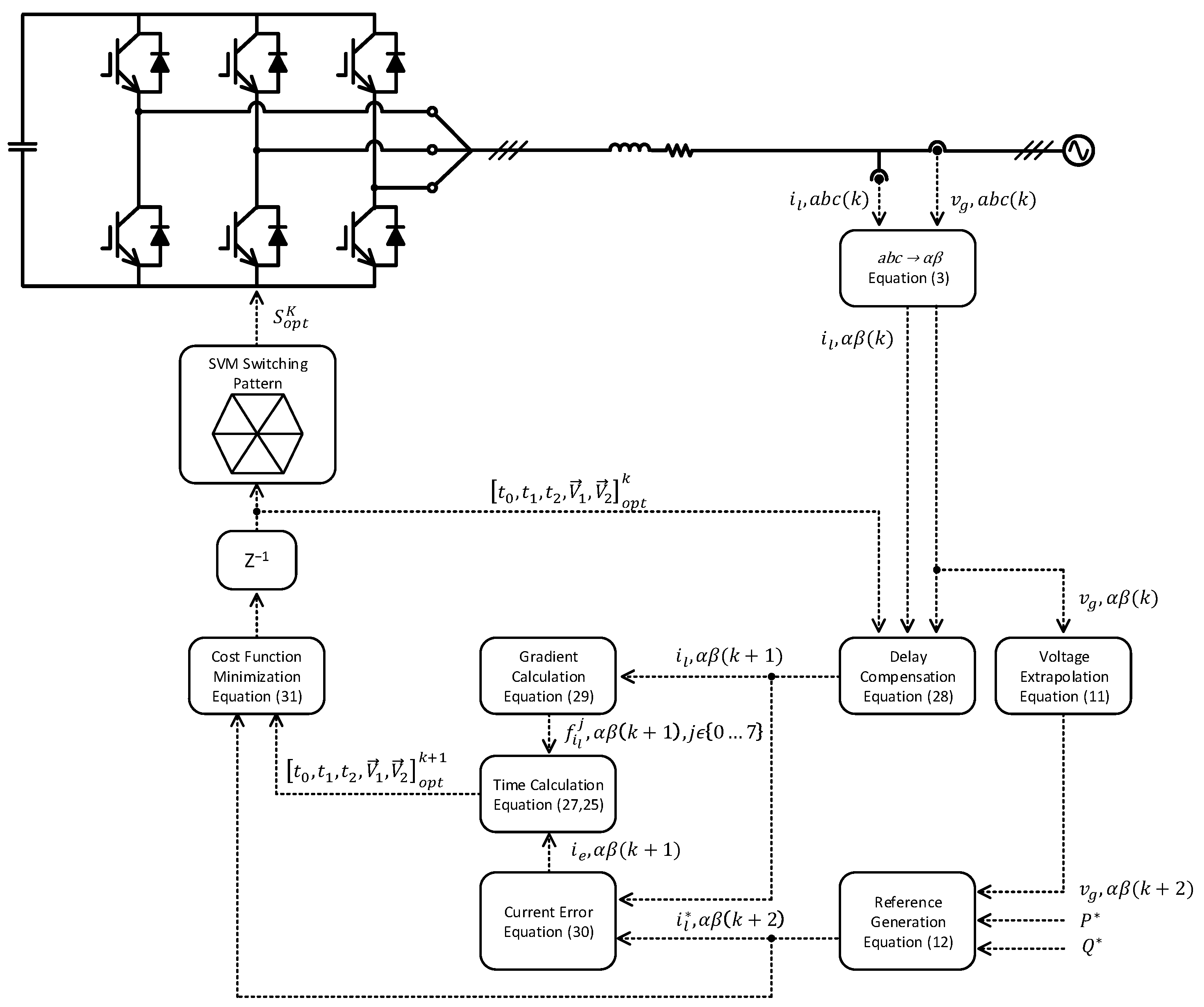
The computational delay compensation is implemented considering the two active and one zero vectors applied to the converter to construct an equivalent vector as presented for M2PC. The OSS-MPC algorithm steps with delay compensation for the converter studied in this paper is shown below. In Figure 9, the block diagram of the converter with OSS-MPC control is presented.
5.1. Predictive Model and Time Calculation
The grid voltages and inductor currents are measured and transformed using the Clarke transformation (Figure 9). In fact, the times and vectors calculated in the previous control period are applied to the converter using the SVM seven-segment pattern. Hence, the predictive model comes from the Equation (4) gradient calculation discretized as shown in Equation (21), where the index represents null and the two active vectors of sector respectively as described in Figure 3. Using Equation (21), the inductor gradients and are directly controlled by the VSI output voltage .
Therefore, the predictive currents can be calculated for sector as follows:
To select the optimum application times of the switching vectors for each , the Lagrange multipliers method, without restrictions, is applied. The sum of the quadratic current future error is minimized by applying Equations (23) and (24).
where and are the predicted inductor current errors. The null vector application time is not considered in Equation (23) as it can be eliminated from Equation (22) using Equation (25).
The optimum time values and local minimum presented in Equation (23) are obtained by applying the optimization conditions presented in Equation (26).
Solving Equation (26), the optimum application times for each sector are calculated using Equation (27). In Appendix A, the Matlab code used to solve Equation (26) is presented.
5.2. Delay Compensation
The delay compensation for OSS-MPC is implemented in the corrections of the gradients and current error terms in Equation (27). As presented for M2PC, Equation (14) is used to calculate the inductor current value. The difference between the two compensation algorithms is that for OSS-MPC the gradients for the two optimum vectors and the null vector are already calculated from the previous . The delay compensation for the inductor current is given by Equation (28):
where , , and are the optimum gradients and times obtained from the previous , respectively.
Thus, the compensated gradients can be calculated as:
Considering the extrapolated reference, the current error used in Equation (27) is compensated with the future error as follows:
5.3. Reference Generation
The current reference generation is implemented for OSS-MPC exactly as it is implemented in Section 3.2 Therefore, the current references and are calculated from Equation (12).
5.4. Cost Function Minimization
The local minimum error for the inductor current is tracked for each sector . With these times and applying the delay compensation, it is possible to elaborate a cost function to select the global optimum sector . The cost function presented in [27,28] is an inter-sample-based type. Therefore, for each sector the cost function is constructed using the gradients and times calculated in Equations (25), (27), and (29). The cost function for sector p is presented in Equation (31).
The inductor currents , are obtained recursively from the calculated times and gradients for each sector . The index represents the vector sequence applied using the order presented in Table 2. The constructed inductor current is calculated as follows:
The current gradients , in Equation (32) are calculated using Equation (29). The initial values , used to construct the signal are equal to the compensated inductor current as presented in Equation (28). Thus, Equation (31) is used to calculate the cost function for the six sectors, choosing the sector with the minimum cost as the optimum. Hence, the times and vector for this sector are applied in the next using the SVM modulator. Figure 10 shows the implemented flowchart of the OSS-MPC controller.
6. Experimental Results
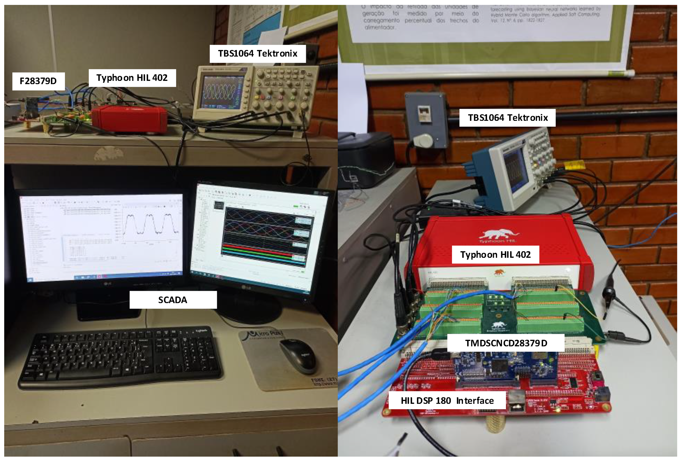
To compare the three FCS-MPC techniques presented in this paper, an experimental setup is implemented using a hardware-in-the-loop (HIL) environment. In fact, the three-phase two-level VSI connected to the grid is implemented virtually in a Typhoon HIL 402 device. Hence, the control techniques are implemented in a Texas Instruments TMDSCNCD28379D control card development board. Indeed, this board uses a C2000™ 200 MHz TMS320F28379D 32-bit floating-point microcontroller designed especially for advanced close-loop control applications [29]. Thus, a supervisory control and data acquisition (SCADA) process is implemented using the Texas Instruments Code Composer Studio 11.2.0 (CCS) and Typhoon Control Center 2022.1 (TCC). Therefore, using SCADA, the data are sent to the microcontroller using the CCS and post processing results is obtained using Matlab. Moreover, a TBS1064 Tektronix oscilloscope is used to observe the variables in the physical domain. The Typhoon HIL 402 physical connection to the control card is implemented using a HIL-DSP-180 interface board especially designed for the Texas Instruments control card. The laboratory experimental configuration and its block diagram are shown in Figure 11 and Figure 12.
The parameters implemented in the HIL 402 and microcontroller and used in the experimental tests are presented in Table 3. The control techniques are evaluated for different steady state and transient scenarios, as presented in the next sections.
6.1. Steady State Results
To evaluate the control techniques in steady state, the power references , are changed for five different scenarios to incorporate the four power quadrants. The power references are set in the controller using the CCS software and the data for post processing are acquired using the TCC (Table 4). The resulting figures are only shown for the power references = 4 kW, = 4 kVAr, since they are similar to the other quadrants. However, to compare the other techniques, Table 4 presents the performance parameters for all the tested scenarios.
6.1.1. Mean Absolut Error (MAE) and Maximum Absolute Error (Emax)
To evaluate the power tracking performance, the MAE and the Emax are calculated for all the power scenarios (Table 4). For the power reference = 4 kW, = 4 kVAr, the reference and measured active and reactive powers for each technique are presented in Figure 13. Analyzing the tracking error, in yellow, it is evident that OSS-MPC is better in steady state, followed by M2PC and OSV-MPC.
To quantify the steady state performance, Equations (33) and (34) are used to calculate the MAE and Emax, where is the total number of samples collected. In Table 4, the tracking performance results for all power references tested are shown. OSS-MPC presented the best results for all scenarios, with much lower MAE and Emax. Then, M2PC presented intermediate results while OSV-MPC generated the worst tracking results.
6.1.2. Current THD
The current harmonic content is an import performance parameter as grid-tie converters must follow legislation limits to be connected to the grid. The current THD is calculated for all the power scenarios presented in Table 4. Figure 14 presents the currents and the harmonic spectrum for each control technique that corresponds to the power reference = 4 kW, = 4 kVAr. Analyzing the currents in Figure 14, OSS-MPC presents much less distortion, followed by M2PC and OSV-MPC. The current THD follows the same order of performance. For all tested scenarios presented in Table 4, OSS-MPC presented better results, followed by M2PC and OSV-MPC.
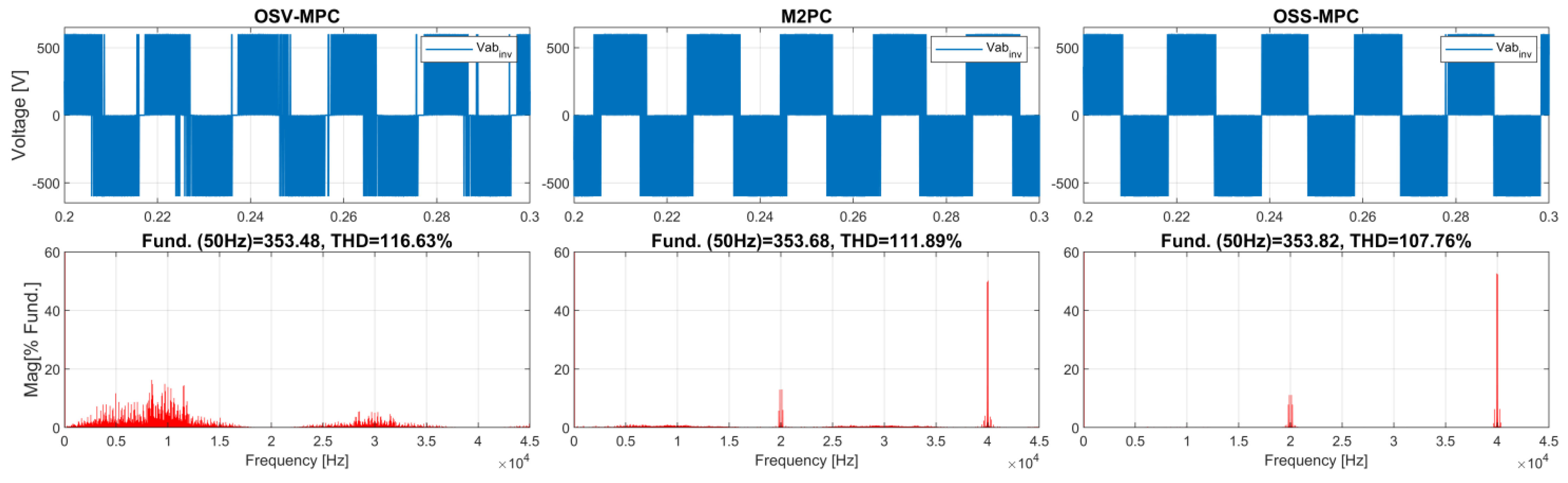
6.1.3. VSI Line Voltage and Spectrum
The VSI output line voltage and its harmonic spectrum are presented in Figure 15 for power references = 4 kW, = 4 kVAr. The modulator used in OSS-MPC and M2PC produces a well-defined harmonic spectrum at the output with the main harmonics multiple of the switching frequency of 20 kHz. The harmonic spectrum of OSV-MPC is spread with much lower frequency concentrations. The high-frequency concentration of OSS-MPC and M2PC facilitates the filter design, in the case of higher order filters, and increases the filter attenuation of the harmonics which improves the steady state results.
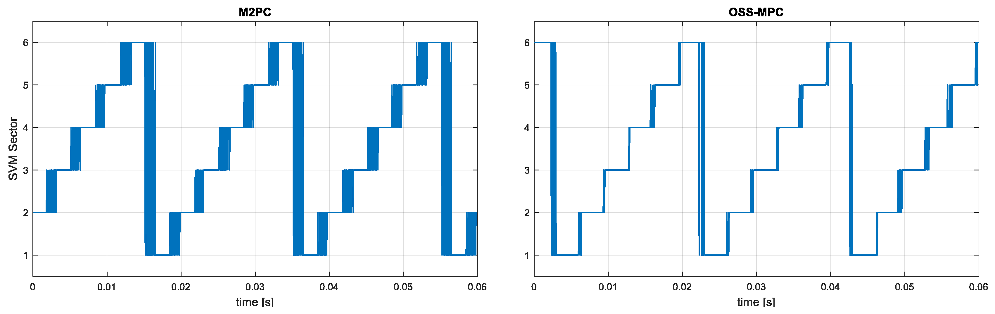
6.1.4. Sector Selection and Duty Ratio
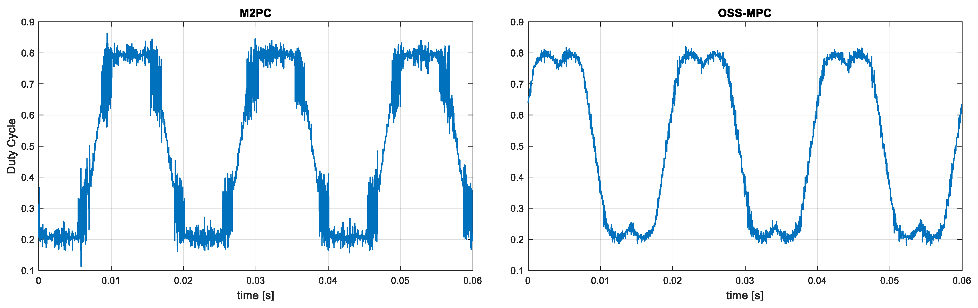
The SVM sector selection and phase a duty ratio for OSS-MPC and M2PC with power references = 4 kW, = 4 kVAr are presented in Figure 16 and Figure 17, respectively. The two optimizations elaborated in the OSS-MPC produce a more precise sector selection than M2PC, and then less transitions between sectors are observed for OSS-MPC. This affects the M2PC duty ratio. The duty ratio for OSS-MPC is similar to the duty ratio expected for a traditional SVM.
6.1.5. Gate Pulse Shape
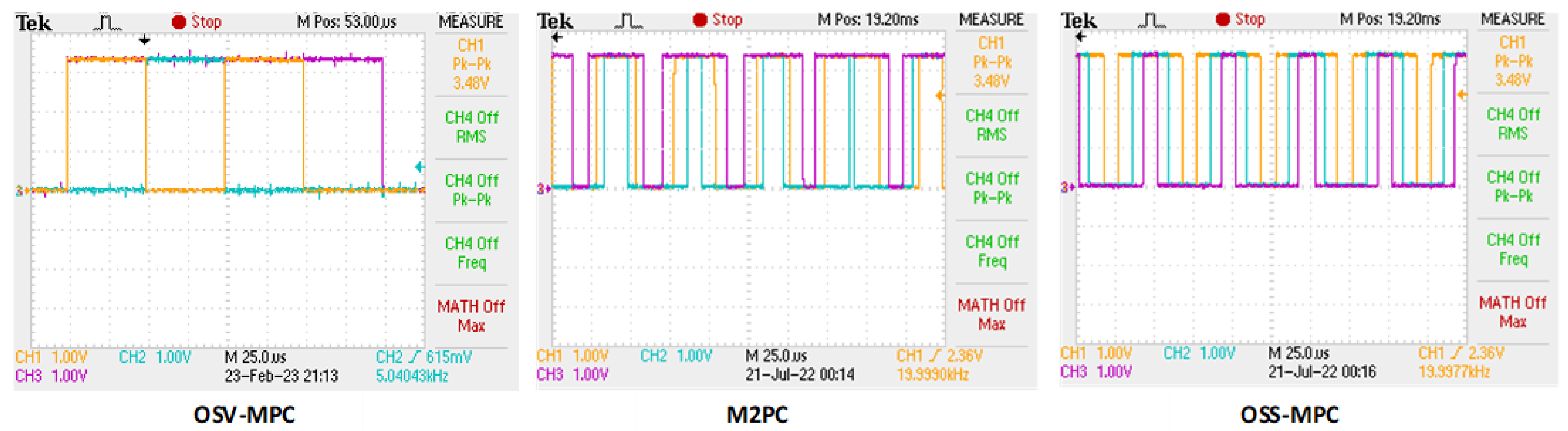
The gate pulse shape (, , and ) for each technique is presented in Figure 18. As expected from the theory, OSV-MPC has no pattern for the switching and produces a variable switching frequency at the output. Owing to the modulation stage, OSS-MPC and M2PC have a well-defined 7-segment switching pattern as presented in Figure 4, with a constant switching frequency of 20 kHz at the output.
6.1.6. Computational Burden
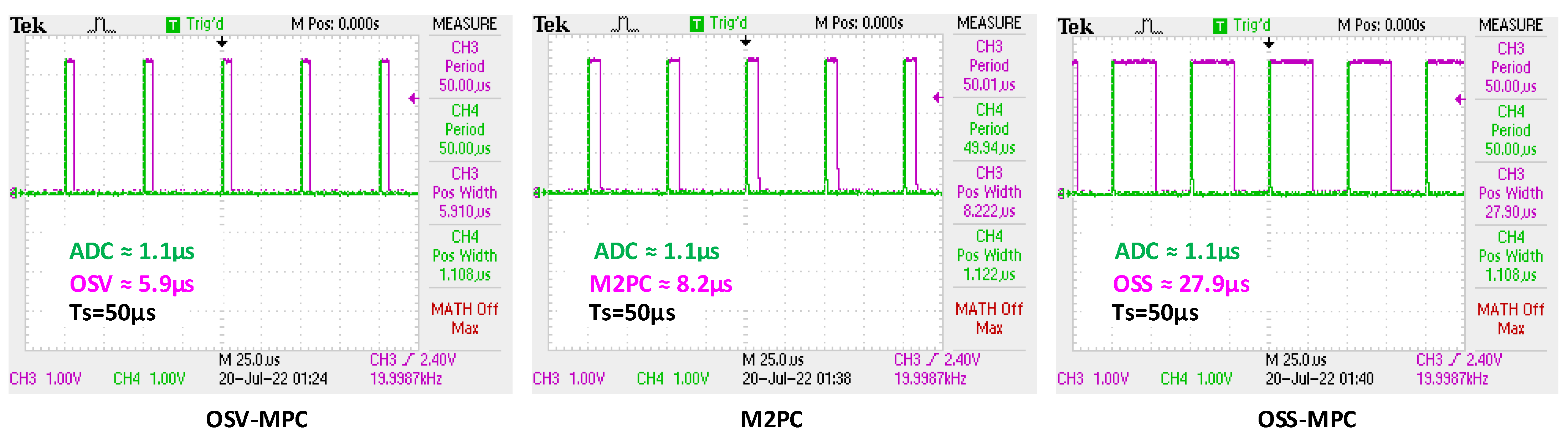
As the FCS-MPC optimization is based on a large number of online calculations, the computational burden is a relevant parameter, as it defines the computational power of the hardware and, consequently, the hardware acquisition cost. The TMS320F28379D microcontroller was able to implement in real time all three FCS-MPC control techniques. Two digital output pins on the microcontroller were used to measure the analog-to-digital (ADC) conversion time and the total, including the ADC, control time. The pins were set to ‘1’ at the beginning of the interruption and set to ‘0’ at the end of the ADC conversion and at the end of the control calculations. Figure 19 shows the computational time for each FCS-MPC technique. The ADC conversion time is about 1.1 µs, which is similar to all the other techniques. The total computational time followed the expected order based on the cost function complexity for the techniques, with OSS-MPC demonstrating the highest time of (27.9 µs), followed by M2PC (8.2 µs) and OSV-MPC (5.9 µs). OSV-MPC and M2PC have large margins to increase the sampling frequency.
6.1.7. Steady State Results Summary
In Table 4, the steady state experimental results for all the tested scenarios are presented. OSS-MPC presented the best results for all steady state parameters, followed by M2PC and OSV-MPC. On the other hand, for the computational time the performance order is inverted. Therefore, there is a trade-off between steady state performance and computational time in the performance of the techniques.
6.2. Transient Results
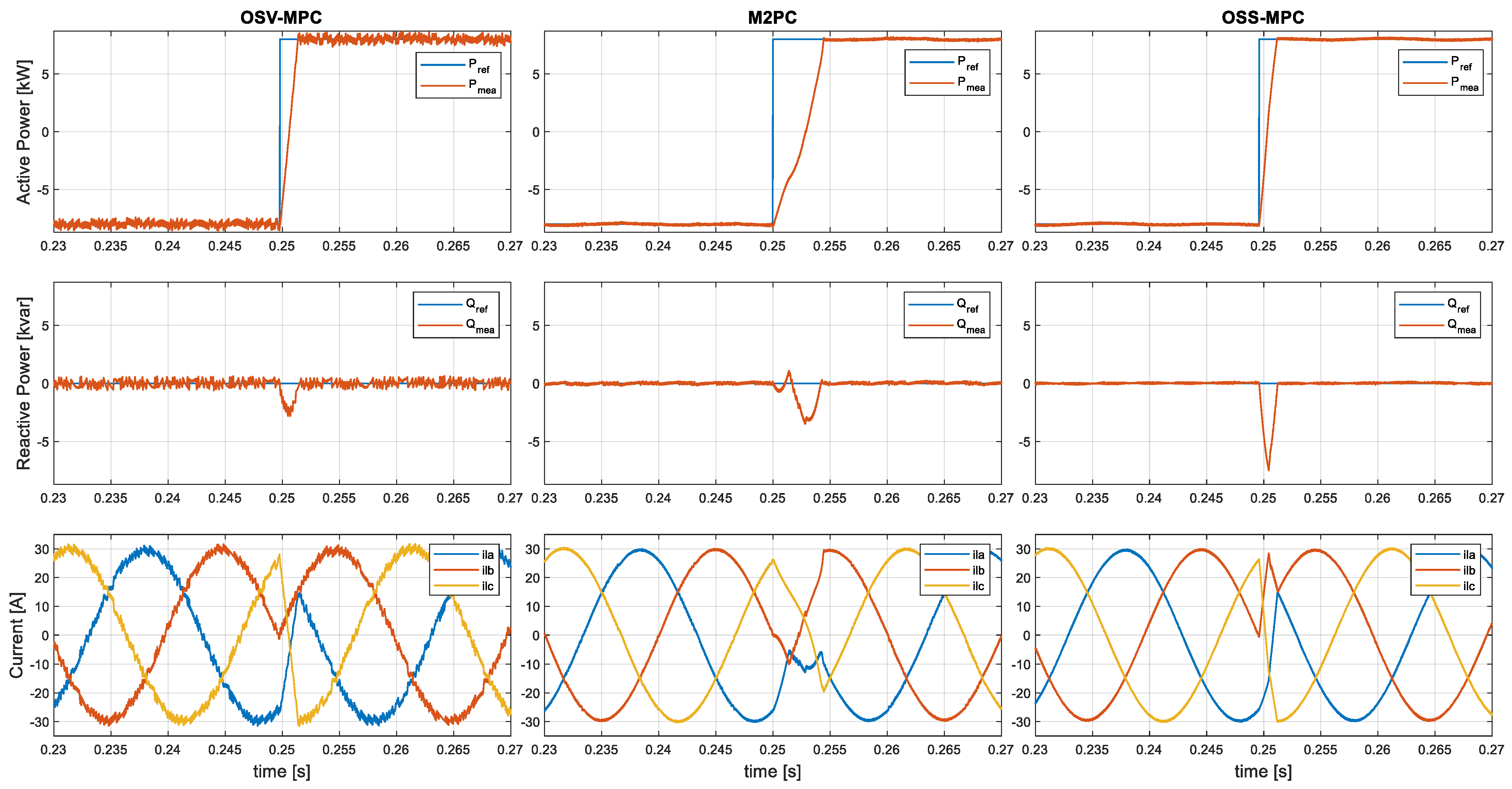
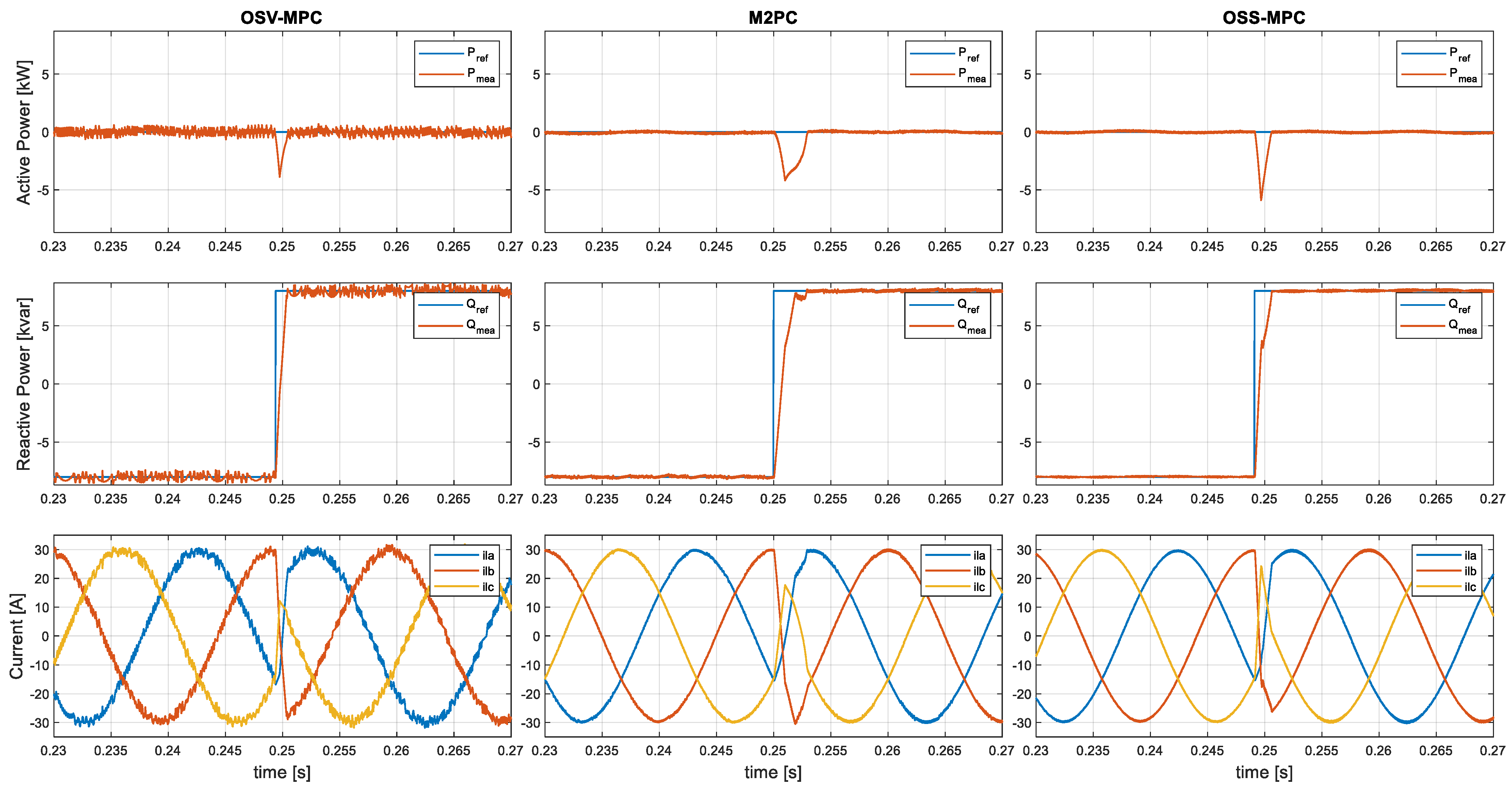
To evaluate the techniques’ transient responses, two different power reference steps were tested. The active power step was implemented from = −8 kW to = +8 kW with = 0 kVAr, and the reactive power step was implemented from = −8 kVAr to = +8 kVAr with = 0 kW. Figure 20 and Figure 21 present the results for the active and reactive power steps, respectively. The settling time was measured directly from the step responses in Figure 20 and Figure 21 using Matlab by applying a 5% margin for each technique (Table 5), which show that OSV-MPC and OSS-MPC presented the lowest settling times and M2PC presented the highest one. All the techniques demonstrated a good transient response as they achieved the desired reference value in less than a quarter of the grid period.
A qualitative comparison between the techniques based on the results and the theory. They are presented in Table 6.
7. Conclusions
This research paper studied the FCS-MPC method, which is a promising technique to control power converters characterized by the incorporation of multiple control loops in a single predictive control law, flexibility to control linear and non-linear systems, and the possibility to include multiple control objectives and restrictions in a single cost function. This research paper presented an experimental comparison between three of the most popular FCS-MPC techniques that could in the near future be substitutes to the classical linear control in many applications. The techniques were compared for steady state and transient conditions. As the computational cost is one of the main drawbacks of FCS-MPC, M2PC is the strategy that demonstrated superior overall results, fulfilling a commitment between computational cost, performance, and simplicity. For future research works, a long prediction horizon approach should be evaluated as a possibility to improve the parameters’ performance for all the techniques.
Author Contributions
Conceptualization, B.V.C. and L.F.E.; formal analysis, B.V.C.; funding acquisition, I.Y. and L.F.E.; methodology, B.V.C. and L.F.E.; project administration, I.Y. and L.F.E.; software, B.V.C.; supervision, L.F.E.; validation, B.V.C., D.C. and L.F.E.; visualization, B.V.C.; writing—original draft, B.V.C.; writing—review and editing, B.V.C., I.Y. and L.F.E. All authors have read and agreed to the published version of the manuscript.
Funding
This research was funded by the National Council for Scientific and Technological Development—CNPq (grant numbers 409024/2021-0 and 311848/2021-4) and the Espírito Santo Research and Innovation Support Foundation—FAPES (grant numbers 514/2021, 668/2022, and 1024/2022). Yahyaoui is funded by the PROEMRED Project, M3010, financed by the University of Rey Juan Carlos, Spain.
Conflicts of Interest
The authors declare no conflict of interest.
Appendix A. Equation (26) Matlab Solution
To solve Equation (26), the symbolic equation solver in Matlab was used. The code is presented below:
clear all
syms t1 t2 Ts % Times
syms ie_ak ie_bk % Current error aplha and beta
syms fi_ak_0 fi_ak_1 fi_ak_2 % Current gradients alpha
syms fi_bk_0 fi_bk_1 fi_bk_2 % Current gradients beta
Rodriguez, J.; Cortes, P. Predictive Control of Power Converters and Electrical Drives; Wiley: Hoboken, NJ, USA, 2012. [Google Scholar]
Kouro, S.; Perez, M.; Rodriguez, J.; Llor, A.; Young, H.A. Model Predictive Control: MPC’s Role in the Evolution of Power Electronics. IEEE Ind. Electron. Mag.2015, 9, 8–21. [Google Scholar] [CrossRef]
Rodriguez, J.; Kazmierkowski, M.P.; Espinoza, J.R.; Zanchetta, P.; Abu-Rub, H.; Young, H.A.; Rojas, C.A. State of the Art of Finite Control Set Model Predictive Control in Power Electronics. IEEE Trans. Ind. Inform.2013, 9, 1003–1016. [Google Scholar] [CrossRef]
Kouro, S.; Cortes, P.; Vargas, R.; Ammann, U.; Rodriguez, J. Model Predictive Control—A Simple and Powerful Method to Control Power Converters. IEEE Trans. Ind. Electron.2009, 56, 1826–1838. [Google Scholar] [CrossRef]
Cortes, P.; Kazmierkowski, M.; Kennel, R.; Quevedo, D.; Rodriguez, J. Predictive Control in Power Electronics and Drives. IEEE Trans. Ind. Electron.2008, 55, 4312–4324. [Google Scholar] [CrossRef]
Vazquez, S.; Rodriguez, J.; Rivera, M.; Franquelo, L.; Norambuena, M. Model Predictive Control for Power Converters and Drives: Advances and Trends. IEEE Trans. Ind. Electron.2017, 64, 935–947. [Google Scholar] [CrossRef] [Green Version]
Hosseinzadeh, M.A.; Sarbanzadeh, M.; Sarebanzadeh, E.; Rivera, M.; Muñoz, J. Predictive Control in Power Converter Applications: Challenge and Trends. In Proceedings of the IEEE International Conference on Automation/XXIII Congress of the Chilean Association of Automatic Control (ICA-ACCA), Greater Concepcion, Chile, 17 October 2018. [Google Scholar]
Ammann, U.; Vargas, R.; Roth-Stielow, J. Investigation of the average switching frequency of Direct Model Predictive Control converters. In Proceedings of the 2010 IEEE International Conference on Industrial Technology, Via del Mar, Chile, 14–17 March 2010. [Google Scholar]
Ramírez, R.O.; Espinoza, J.; Villarroel, F.; Maurelia, E.; Reyes, M.E. A Novel Hybrid Finite Control Set Model Predictive Control Scheme with Reduced Switching. IEEE Trans. Ind. Electron.2014, 61, 5912–5920. [Google Scholar] [CrossRef]
Vazquez, S.; Leon, J.I.; Franquelo, L.G.; Carrasco, J.M.; Martinez, O.; Rodríguez, J.; Cortes, P.; Kouro, S. Model Predictive Control with constant switching frequency using a Discrete Space Vector Modulation with virtual state vectors. In Proceedings of the IEEE International Conference on Industrial Technology, Churchill, Australia, 10–13 February 2009. [Google Scholar]
Aguilera, R.P.; Lezana, P.; Konstantinou, G.; Acuna, P.; Wu, B.; Bernet, S.; Agelidis, V.G. Closed-loop SHE-PWM technique for power converters through Model Predictive Control. In Proceedings of the IECON 2015—41st Annual Conference of the IEEE Industrial Electronics Society, Yokohama, Japan, 9–12 November 2015. [Google Scholar]
Aggrawal, H.; Leon, J.; Franquelo, L.; Kouro, S.; Garg, P.; Rodríguez, J. Model predictive control based selective harmonic mitigation technique for multilevel cascaded H-bridge converters. In Proceedings of the IECON 2011—37th Annual Conference of the IEEE Industrial Electronics Society, Melbourne, Australia, 7–10 November 2011. [Google Scholar]
Cortes, P.; Rodriguez, J.; Quevedo, D.; Silva, C. Predictive Current Control Strategy with Imposed Load Current Spectrum. IEEE Trans. Power Electron.2008, 23, 612–618. [Google Scholar] [CrossRef]
Aguilera, R.P.; Acuna, P.; Lezana, P.; Konstantinou, G.; Wu, B.; Bernet, S.; Agelidis, V.G. Selective Harmonic Elimination Model Predictive Control for Multilevel Power Converters. IEEE Trans. Power Electron.2017, 32, 2416–2426. [Google Scholar] [CrossRef] [Green Version]
Kouro, S.; La Rocca, B.; Cortes, P.; Alepuz, S.; Wu, B.; Rodriguez, J. Predictive control based selective harmonic elimination with low switching frequency for multilevel converters. In Proceedings of the 2009 IEEE Energy Conversion Congress and Exposition, San Jose, CA, USA, 20–24 September 2009. [Google Scholar]
Gannamraju, S.K.; Valluri, D.; Bhimasingu, R. Comparison of Fixed Switching Frequency Based Optimal Switching Vector MPC Algorithms Applied to Voltage Source Inverter for Stand-alone Applications. In Proceedings of the 2019 National Power Electronics Conference (NPEC), Tiruchirappalli, India, 13–15 December 2019. [Google Scholar]
Comarella, B.V.; Encarnação, L.F. Comparison of Model Predictive Control Strategies for Voltage Source Inverter with Output LC Filter. In Proceedings of the 2021 IEEE Southern Power Electronics Conference (SPEC), Kigali, Rwanda, 6–9 December 2021. [Google Scholar]
Hamouda, M.M.; Fnaiech, F. A review of PWM voltage source converters based industrial applications. In Proceedings of the 2015 International Conference on Electrical Systems for Aircraft, Railway, Ship Propulsion and Road Vehicles (ESARS), Aachen, Germany, 3–5 March 2015. [Google Scholar]
Kumar, J. Implementation of Space Vector Modulation for Two Level Inverter and its Comparison with SPWM. Int. J. Adv. Res. Electr. Electron. Instrum. Eng.2015, 4, 5012–5019. [Google Scholar]
Akagi, H.; Watanabe, E.H.; Aredes, M. Instantaneous Power Theory and Applications to Power Conditioning, 2nd ed.; Wiley: Hoboken, NJ, USA, 2017. [Google Scholar]
Vazquez, S.; Leon, J.; Franquelo, L.; Carrasco, J.; Dominguez, E.; Cortes, P.; Rodriguez, J. Comparison between FS-MPC control strategy for an UPS inverter application in α-β and abc frames. In Proceedings of the 2010 IEEE International Symposium on Industrial Electronics, Bari, Italy, 4–7 July 2010. [Google Scholar]
Wu, B. High-Power Converters and AC Drives; Wiley: Hoboken, NJ, USA, 2006. [Google Scholar]
Rodriguez, J.; Pontt, J.; Silva, C.A.; Correa, P.; Lezana, P.; Cortes, P.; Ammann, U. Predictive Current Control of a Voltage Source Inverter. IEEE Trans. Ind. Electron.2007, 54, 495–503. [Google Scholar] [CrossRef]
Cortes, P.; Rodriguez, J.; Silva, C.; Flores, A. Delay Compensation in Model Predictive Current Control of a Three-Phase Inverter. IEEE Trans. Ind. Electron.2011, 59, 1323–1325. [Google Scholar] [CrossRef]
Rivera, M.; Morales, F.; Baier, C.; Munoz, J.; Tarisciotti, L.; Zanchetta, P.; Wheeler, P. A modulated model predictive control scheme for a two-level voltage source inverter. In Proceedings of the 2015 IEEE International Conference on Industrial Technology (ICIT), Seville, Spain, 17–19 March 2015. [Google Scholar]
Rivera, M.; Riveros, J.; Rodríguez, C.; Wheeler, P. Predictive Control Operating at Fixed Switching Frequency of an Induction Machine Fed by a Voltage Source Inverter. In Proceedings of the 2021 IEEE International Conference on Automation/XXIV Congress of the Chilean Association of Automatic Control (ICA-ACCA), Valparaíso, Chile, 22–26 March 2021. [Google Scholar]
Zheng, C.; Dragičević, T.; Zhang, Z.; Rodriguez, J.; Blaabjerg, F. Model Predictive Control of LC-Filtered Voltage Source Inverters with Optimal Switching Sequence. IEEE Trans. Power Electron.2021, 36, 3422–3436. [Google Scholar] [CrossRef]
Vazquez, S.; Marquez, A.; Aguilera, R.; Quevedo, D.; Leon, J.; Franquelo, L.G. Predictive Optimal Switching Sequence Direct Power Control for Grid-Connected Power Converters. IEEE Trans. Ind. Electron.2015, 62, 2010–2020. [Google Scholar] [CrossRef] [Green Version]
Figure 13.
Output active and reactive power for each FCS-MPC technique for = 4 kW, = 4 kVAr.
Figure 13.
Output active and reactive power for each FCS-MPC technique for = 4 kW, = 4 kVAr.
Figure 14.
Output voltage, current, and current spectrum for each FCS-MPC technique for = 4 kW, = 4 kVAr.
Figure 14.
Output voltage, current, and current spectrum for each FCS-MPC technique for = 4 kW, = 4 kVAr.
Figure 15.
Output VSI line voltage and spectrum for each FCS-MPC technique for = 4 kW, = 4 kVAr.
Figure 15.
Output VSI line voltage and spectrum for each FCS-MPC technique for = 4 kW, = 4 kVAr.
Figure 16.
Comparison of phase a SVM sector selection for M2PC and OSS-MPC for = 4 kW, = 4 kVAr (obtained from CCS).
Figure 16.
Comparison of phase a SVM sector selection for M2PC and OSS-MPC for = 4 kW, = 4 kVAr (obtained from CCS).
Figure 17.
Comparison of phase a duty ratio for M2PC and OSS-MPC for = 4 kW, = 4 kVAr (obtained from CCS).
Figure 17.
Comparison of phase a duty ratio for M2PC and OSS-MPC for = 4 kW, = 4 kVAr (obtained from CCS).
Figure 18.
Comparison of switching pattern for each FCS-MPC technique.
Figure 18.
Comparison of switching pattern for each FCS-MPC technique.
Figure 19.
Comparison of ADC converter time and total computational time for each FCS-MPC technique.
Figure 19.
Comparison of ADC converter time and total computational time for each FCS-MPC technique.
Figure 20.
Transient response for active power step = −8 kW to = +8 kW for each FCS-MPC technique.
Figure 20.
Transient response for active power step = −8 kW to = +8 kW for each FCS-MPC technique.
Figure 21.
Transient response for active power step = −8 kVAr to = +8 kVAr for each FCS-MPC technique.
Figure 21.
Transient response for active power step = −8 kVAr to = +8 kVAr for each FCS-MPC technique.
Table 1.
Possible switching states for the two-level VSI and space vectors generated.
Table 1.
Possible switching states for the two-level VSI and space vectors generated.
Applied Vector
Switching State [S1 S3 S5]
Space Vector
[0, 0, 0]
0
[1, 0, 0]
[1, 1, 0]
[0, 1, 0]
[0, 1, 1]
[0, 0, 1]
[1, 0, 1]
[1, 1, 1]
0
Table 2.
Seven-segment switching sequence and application times.
Table 2.
Seven-segment switching sequence and application times.
Sector
Vector Sequence
Application Times Sequence
[, , , , , , , ]
[t0, t1, t2, t0, t0, t2, t1, t0]
[, , , , , , , ]
[t0, t2, t1, t0, t0, t1, t2, t0]
[, , , , , , , ]
[t0, t1, t2, t0, t0, t2, t1, t0]
[, , , , , , , ]
[t0, t2, t1, t0, t0, t1, t2, t0]
[, , , , , , , ]
[t0, t1, t2, t0, t0, t2, t1, t0]
[, , , , , , , ]
[t0, t2, t1, t0, t0, t1, t2, t0]
Table 3.
Parameters used in the experimental tests.
Table 3.
Parameters used in the experimental tests.
Parameter
Value
DC bus voltage
= 600 Vdc
Grid voltage and frequency
= 127 Vrms, = 50 Hz
Filter inductance
= 5 mH
Filter resistance
= 1 mΩ
Active power reference
= Variable
Reactive power reference
= Variable
Sampling time
= 50 µs
Switching frequency
20 kHz (variable for OSV-MPC)
ADC resolution
12 bits
PWM counter (resolution)
2500
Table 4.
Steady state experimental results.
Table 4.
Steady state experimental results.
Strategy
Power Reference
Emax
MAE
THDi (%)
Computational Time (µs)
P (kW)
Q (kVAr)
P (W)
Q (var)
P (W)
Q (var)
OSV-MPC
0
0
651.97
716.96
168.90
189.84
-
5.9
4
4
662.98
695.51
170.23
191.30
5.39
−4
4
724.43
696.20
174.67
193.20
5.59
4
−4
653.94
650.02
170.74
204.78
5.82
−4
−4
678.55
645.24
172.94
207.87
5.65
M2PC
0
0
217.91
227.53
42.43
58.33
-
8.2
4
4
229.50
247.11
43.80
58.37
1.46
−4
4
210.21
237.29
45.92
56.82
1.47
4
−4
241.97
253.80
57.62
59.76
1.51
−4
−4
251.22
240.79
59.76
58.26
1.49
OSS-MPC
0
0
156.65
154.33
36.61
28.42
-
27.9
4
4
181.45
174.65
42.94
35.72
1.03
−4
4
223.56
170.32
45.01
33.97
1.02
4
−4
170.11
154.67
43.60
28.48
0.97
−4
−4
209.92
147.80
45.55
26.49
0.96
Table 5.
Transient experimental results.
Table 5.
Transient experimental results.
Strategy
Settling Time (ms)
Active Power Step
Reactive Power Step
OSV-MPC
1.8
1.0
M2PC
4.4
2.9
OSS-MPC
1.6
1.5
Table 6.
Comparison between OSV-MPC, M2PC, and OSS-MPC.
Table 6.
Comparison between OSV-MPC, M2PC, and OSS-MPC.
Parameter
OSV-MPC
M2PC
OSS-MPC
Cost function
Vector based
Sector based
Inter-sample sector based
Single vector (1)
Multiple vectors (8)
Multiple vectors (8)
Switching frequency
Variable
Fixed
Fixed
Modulator
No
Yes
Yes
Steady state performance
Moderate
Good
Better
Transient performance
Good
Moderate
Good
Computational cost
Low
Low
High
Disclaimer/Publisher’s Note: The statements, opinions and data contained in all publications are solely those of the individual author(s) and contributor(s) and not of MDPI and/or the editor(s). MDPI and/or the editor(s) disclaim responsibility for any injury to people or property resulting from any ideas, methods, instructions or products referred to in the content.
Comarella, B.V.; Carletti, D.; Yahyaoui, I.; Encarnação, L.F.
Theoretical and Experimental Comparative Analysis of Finite Control Set Model Predictive Control Strategies. Electronics2023, 12, 1482.
https://doi.org/10.3390/electronics12061482
AMA Style
Comarella BV, Carletti D, Yahyaoui I, Encarnação LF.
Theoretical and Experimental Comparative Analysis of Finite Control Set Model Predictive Control Strategies. Electronics. 2023; 12(6):1482.
https://doi.org/10.3390/electronics12061482
Chicago/Turabian Style
Comarella, Breno Ventorim, Daniel Carletti, Imene Yahyaoui, and Lucas Frizera Encarnação.
2023. "Theoretical and Experimental Comparative Analysis of Finite Control Set Model Predictive Control Strategies" Electronics 12, no. 6: 1482.
https://doi.org/10.3390/electronics12061482
Note that from the first issue of 2016, this journal uses article numbers instead of page numbers. See further details here.
Article Metrics
No
No
Article Access Statistics
For more information on the journal statistics, click here.
Multiple requests from the same IP address are counted as one view.
Comarella, B.V.; Carletti, D.; Yahyaoui, I.; Encarnação, L.F.
Theoretical and Experimental Comparative Analysis of Finite Control Set Model Predictive Control Strategies. Electronics2023, 12, 1482.
https://doi.org/10.3390/electronics12061482
AMA Style
Comarella BV, Carletti D, Yahyaoui I, Encarnação LF.
Theoretical and Experimental Comparative Analysis of Finite Control Set Model Predictive Control Strategies. Electronics. 2023; 12(6):1482.
https://doi.org/10.3390/electronics12061482
Chicago/Turabian Style
Comarella, Breno Ventorim, Daniel Carletti, Imene Yahyaoui, and Lucas Frizera Encarnação.
2023. "Theoretical and Experimental Comparative Analysis of Finite Control Set Model Predictive Control Strategies" Electronics 12, no. 6: 1482.
https://doi.org/10.3390/electronics12061482
Note that from the first issue of 2016, this journal uses article numbers instead of page numbers. See further details here.


