


One-Dimensional Maximum Power Point Tracking Design of Switched-Capacitor Charge Pumps for Thermoelectric Energy Harvesting
Abstract
:1. Introduction
2. Previous Work on TEG-CP System with MPPT and Reconfigurable CP
2.1. 2D (N, f) MPPT [13]
- (Step 1) N is set to be the maximum assuming VOC is at the minimum (otherwise, the output voltage cannot reach the target output voltage VPP_TGT). f is set to be the minimum for having room to increase the input power to the CP with faster f during the following searching procedure.
- (Step 2) CP runs in a predetermined period Tp. The peak output voltage is measured as VPP_past.
- (Step 3) CP runs in Tp with a decreased N. The peak output voltage is measured as VPP_now.
- (Step 4) VPP_now is compared with VPP_past. If VPP_now > VPP_past, then Step 3 is done. Otherwise, the procedure moves on to Step 5.
- (Step 5) N is considered optimum at the current VOC, which makes the CP to output the maximum IPP.
- 6.
- (Step 6) CP runs in Tp with an increased f. The peak output voltage is measured as VPP_now.
- 7.
- (Step 7) VPP_now is compared with VPP_past. If VPP_now > VPP_past, then Step 6 is done. Otherwise, the procedure stops.
2.2. 2D (N, f) MPPT Algorism for CP System with a Supercapacitor and a Linear Regulator [14]
2.3. 3D (C, N, f) MPPT Algorism [15]
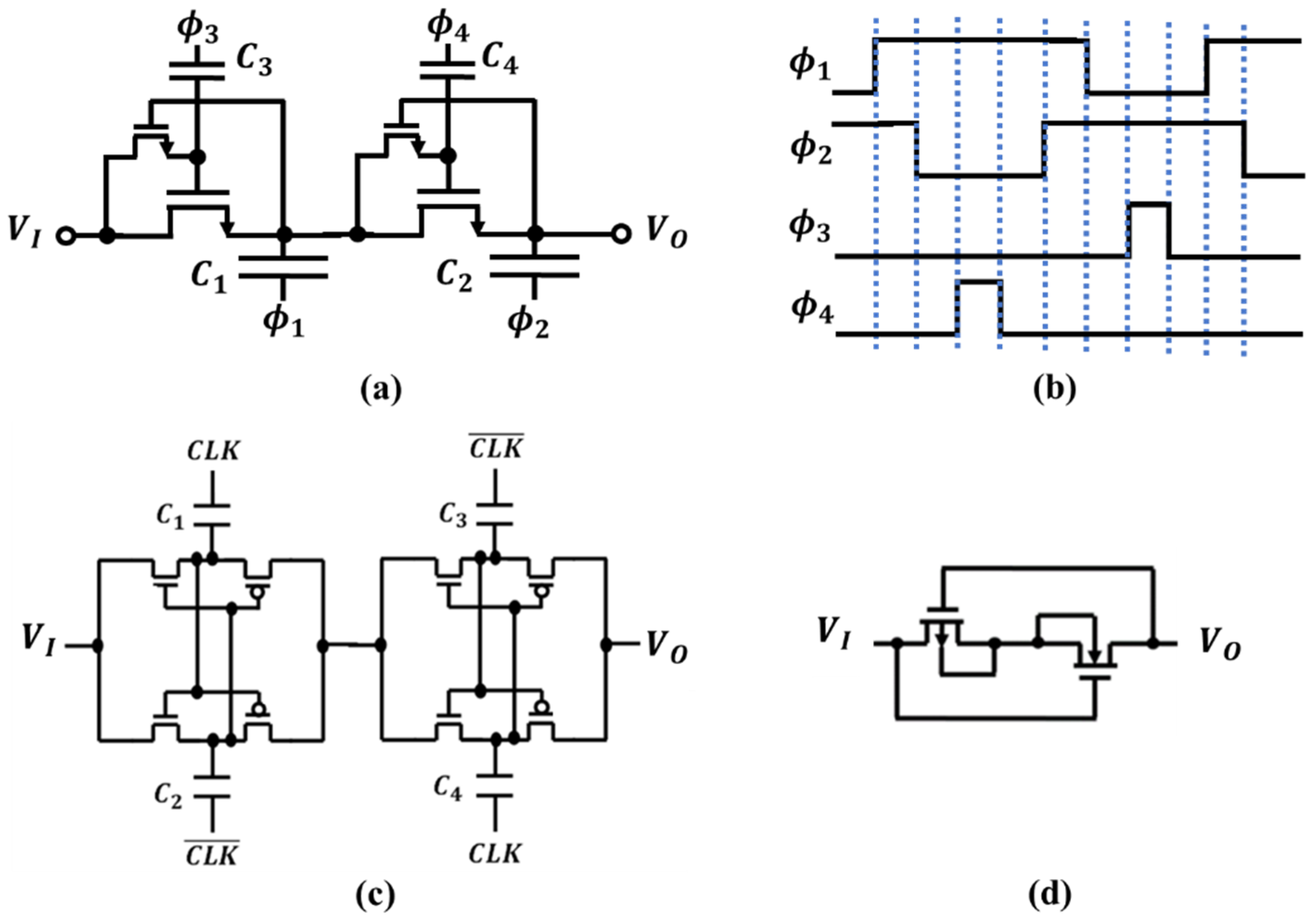
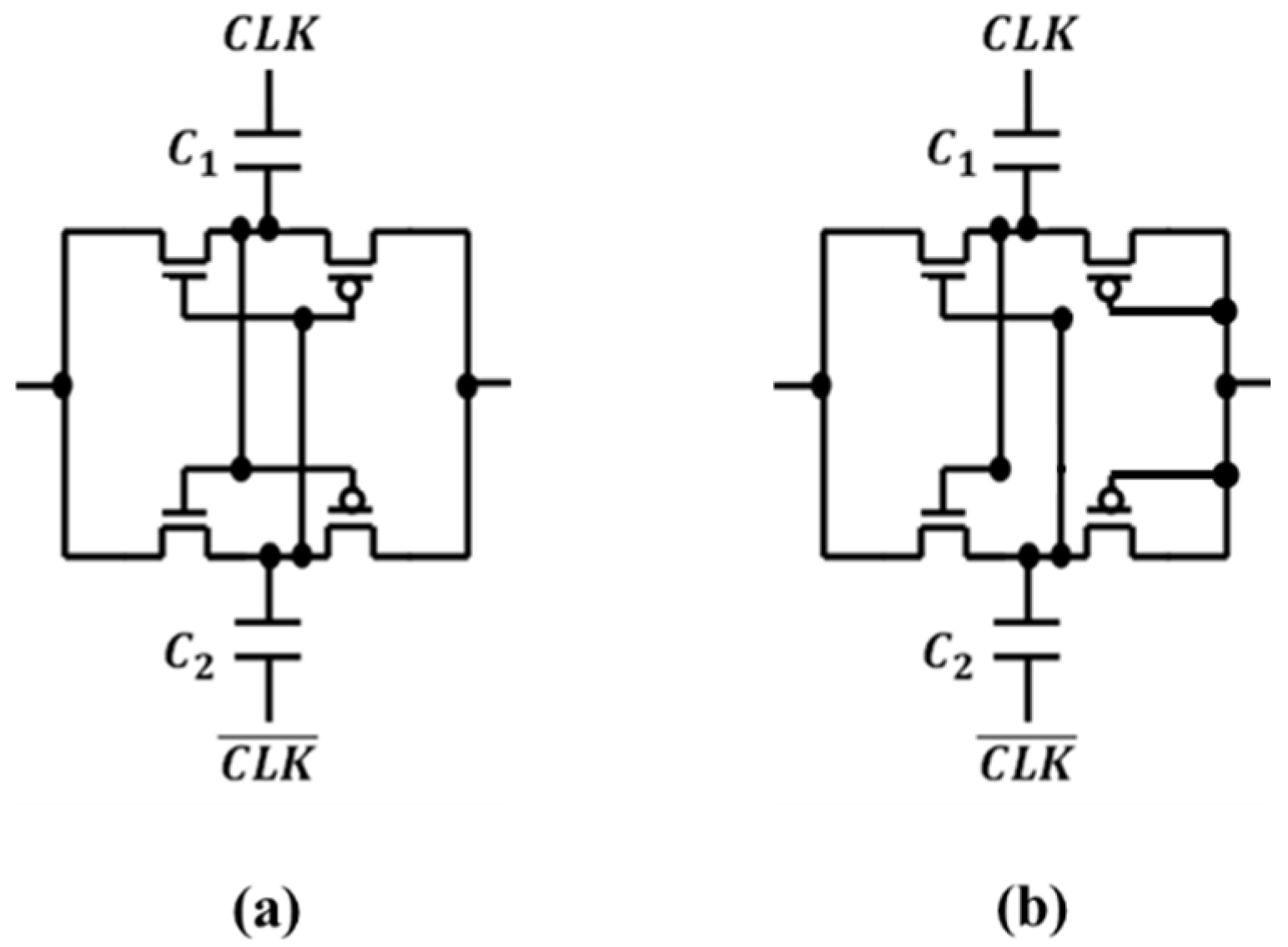
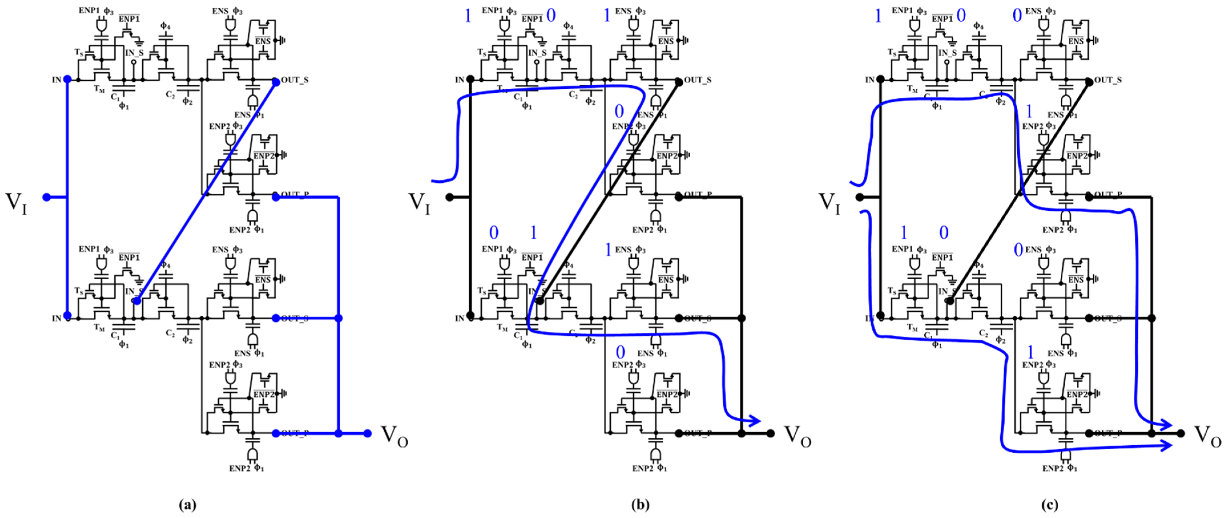
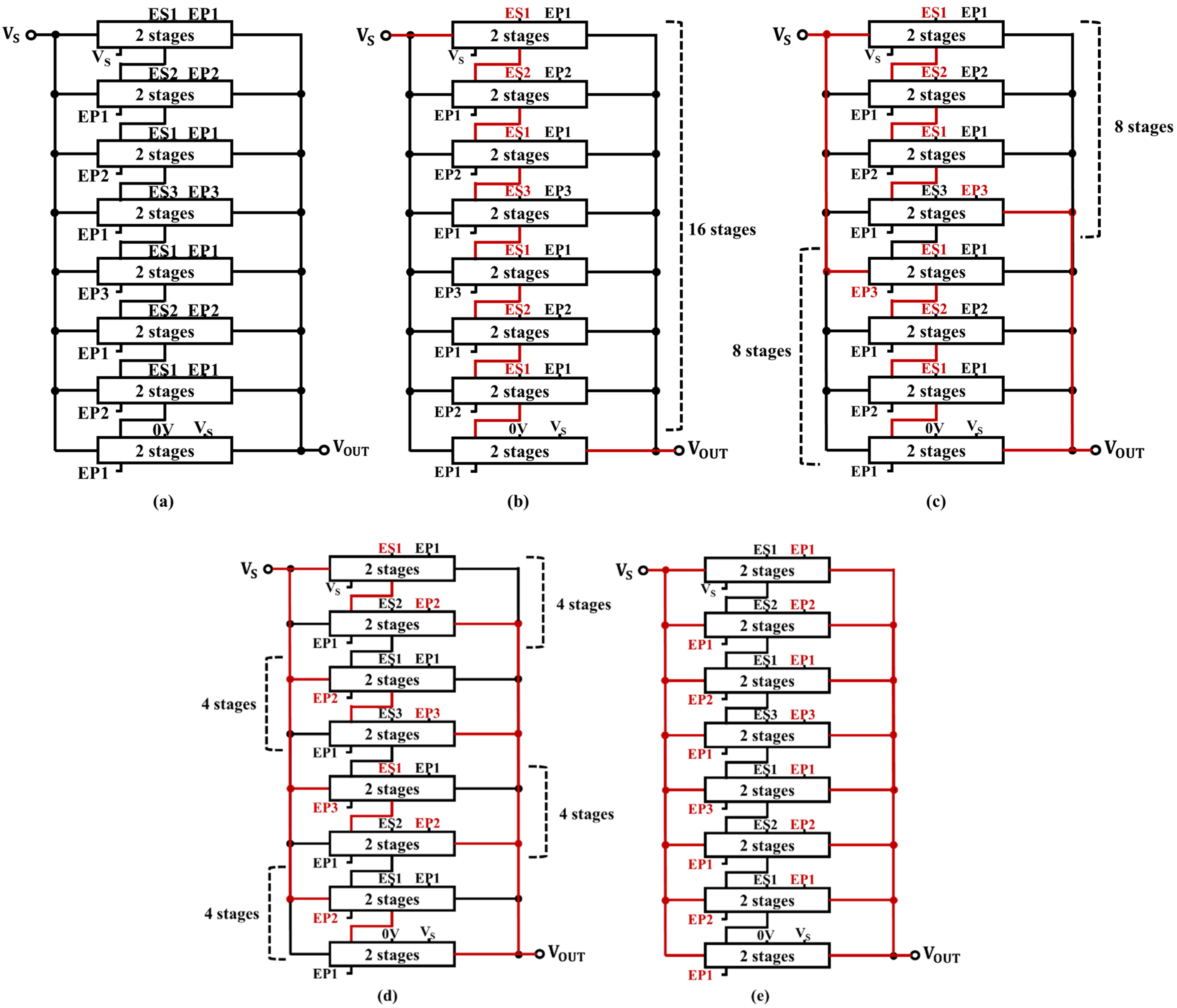
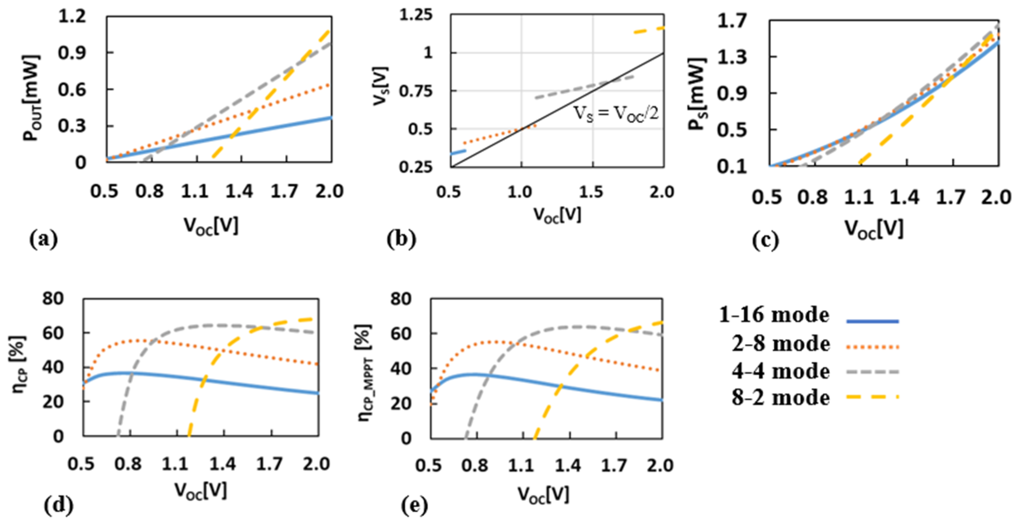
2.4. Reconfigurable CP
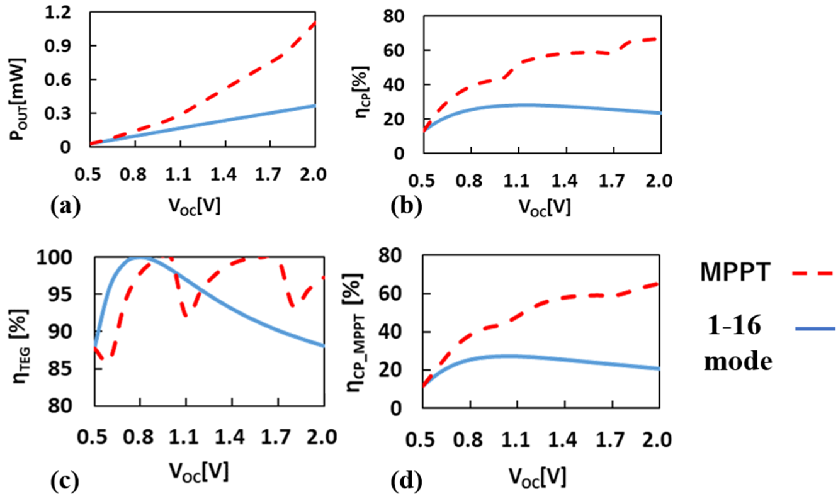
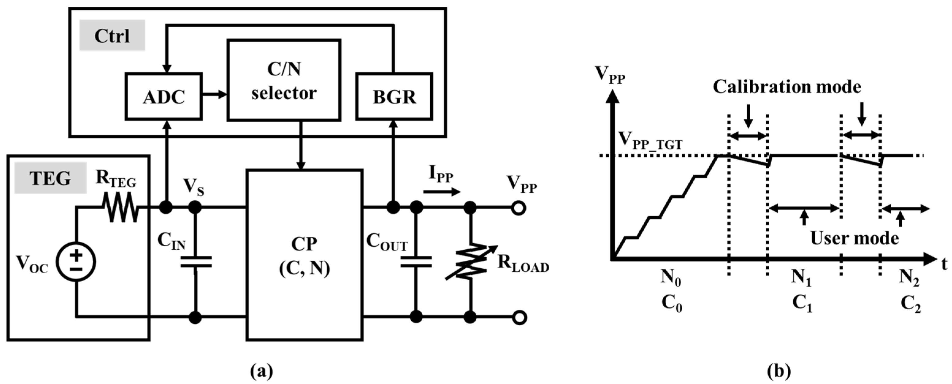
3. Concept of 1D MPPT
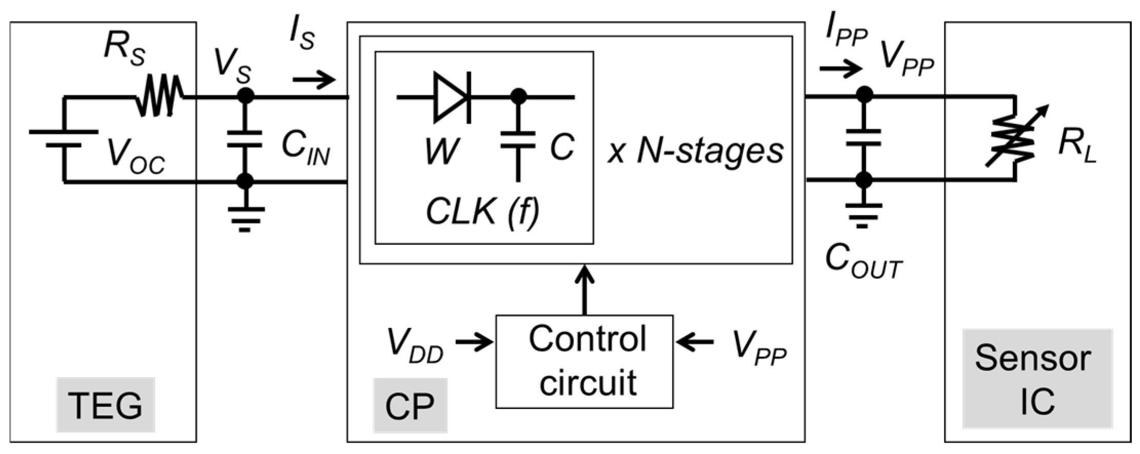
4. Circuit Design
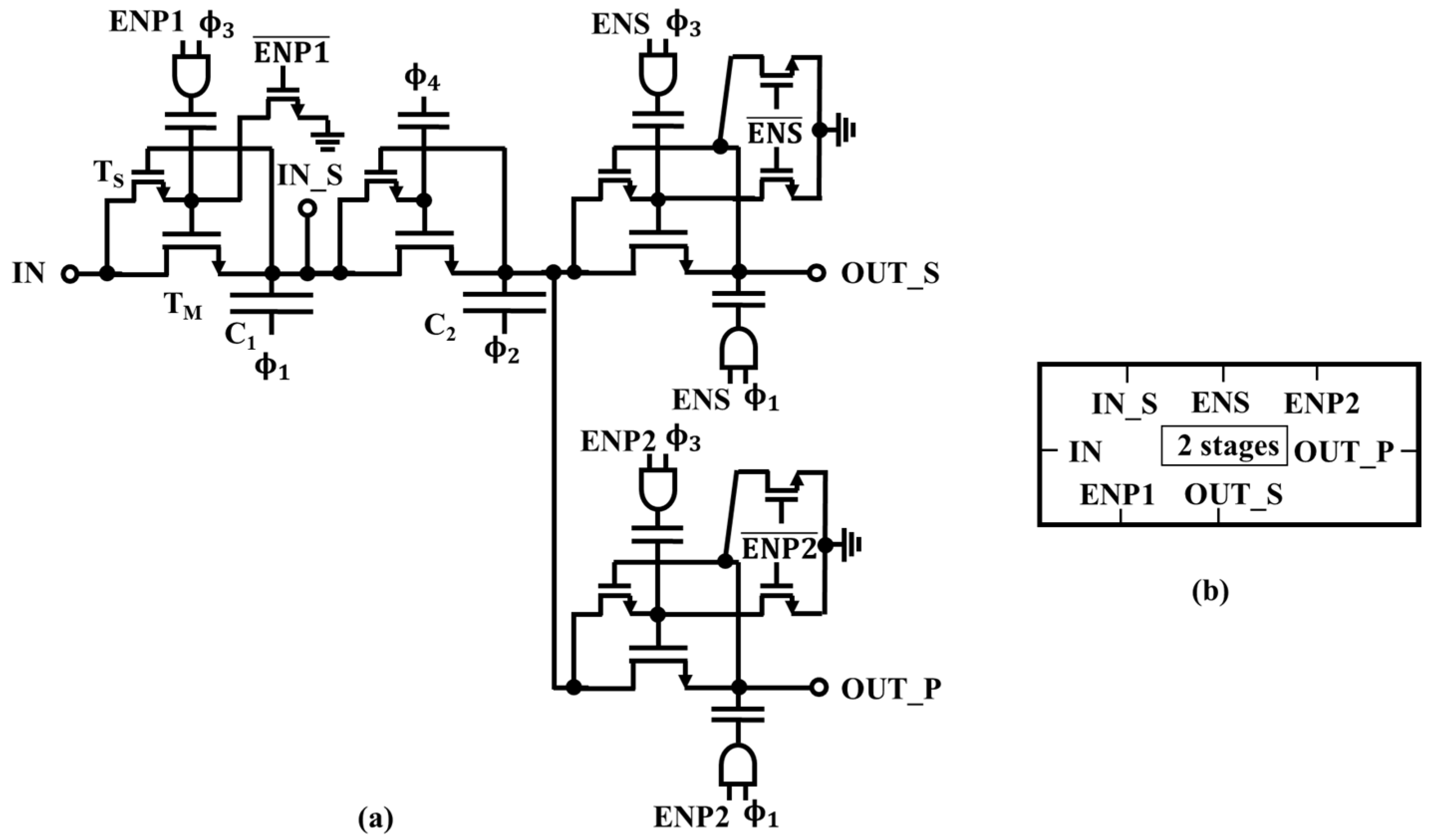
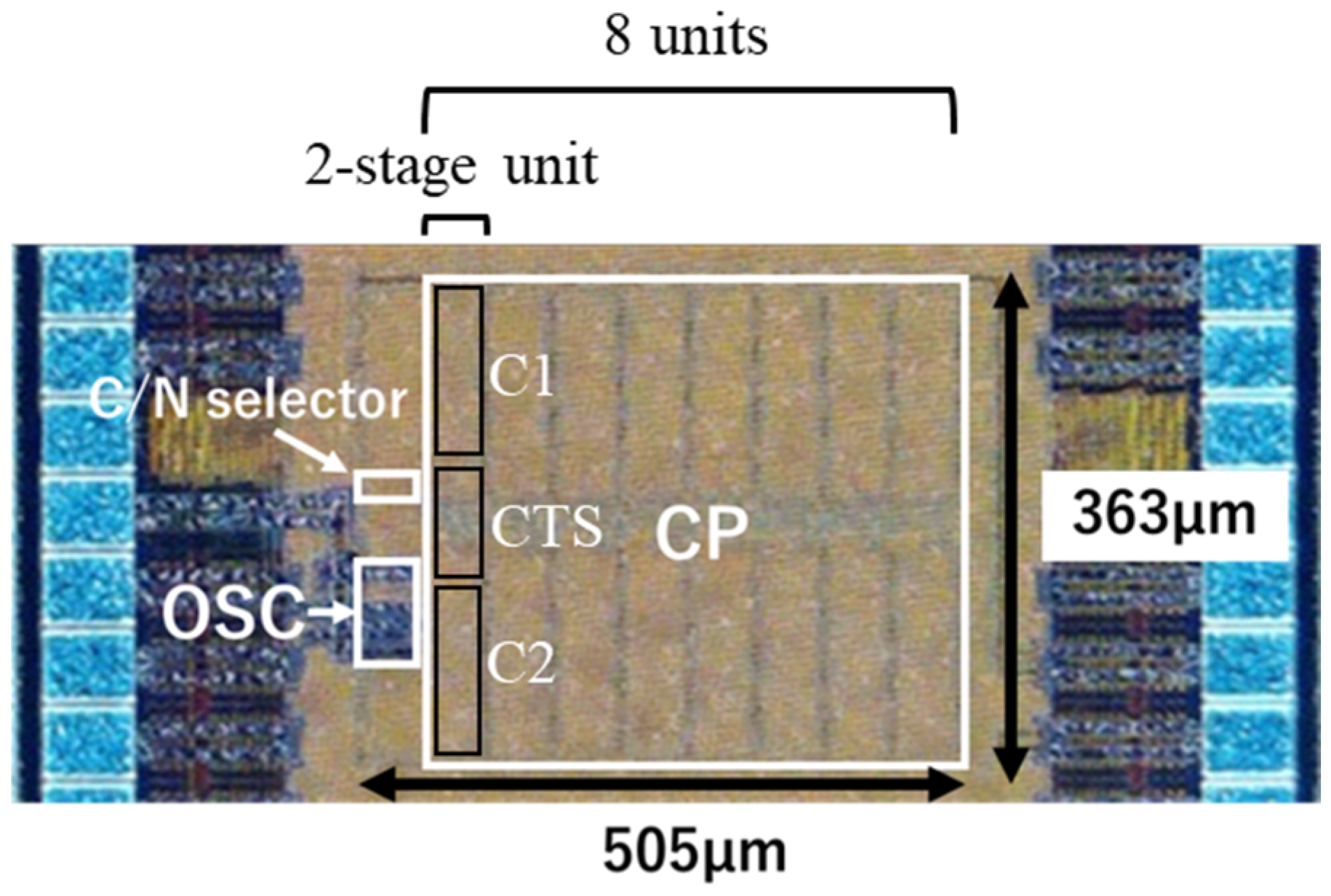
4.1. Reconfigurable CP
4.2. System Design
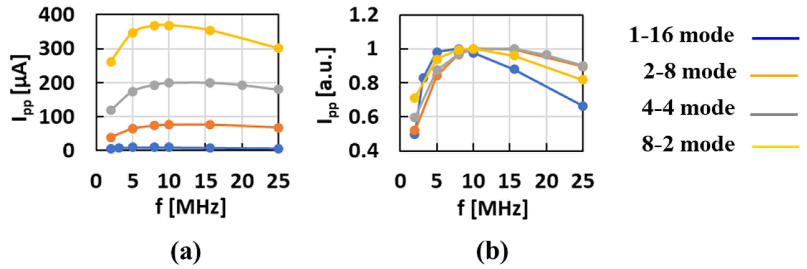
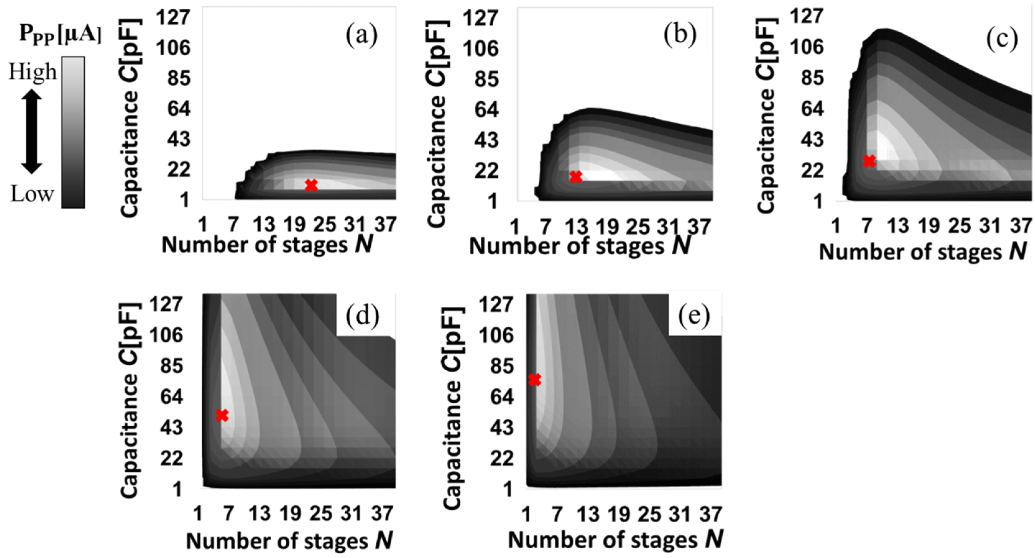
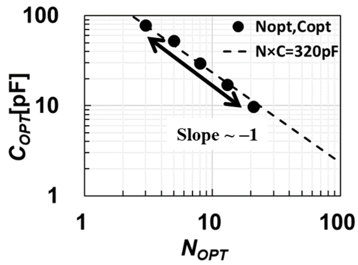
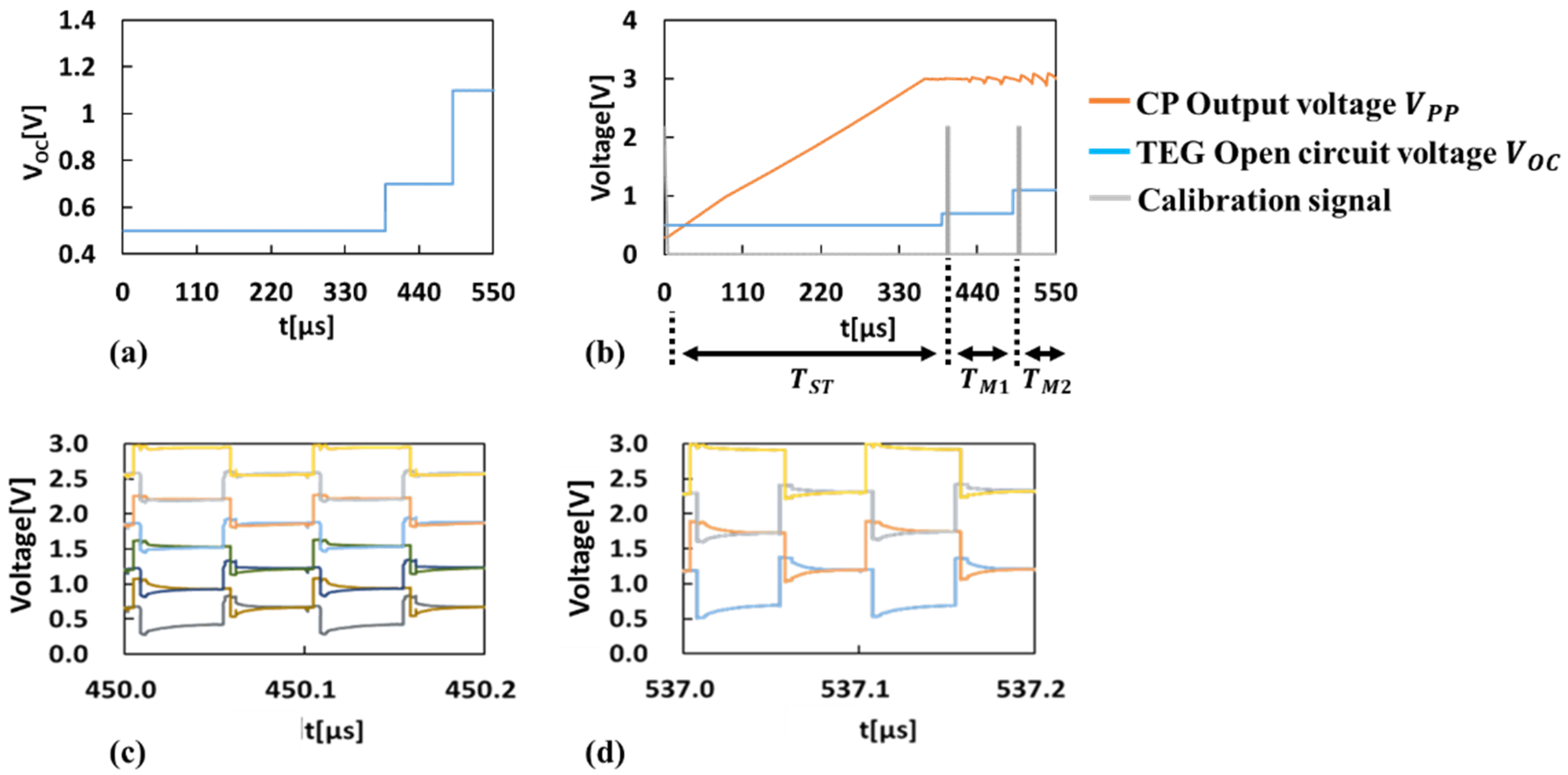
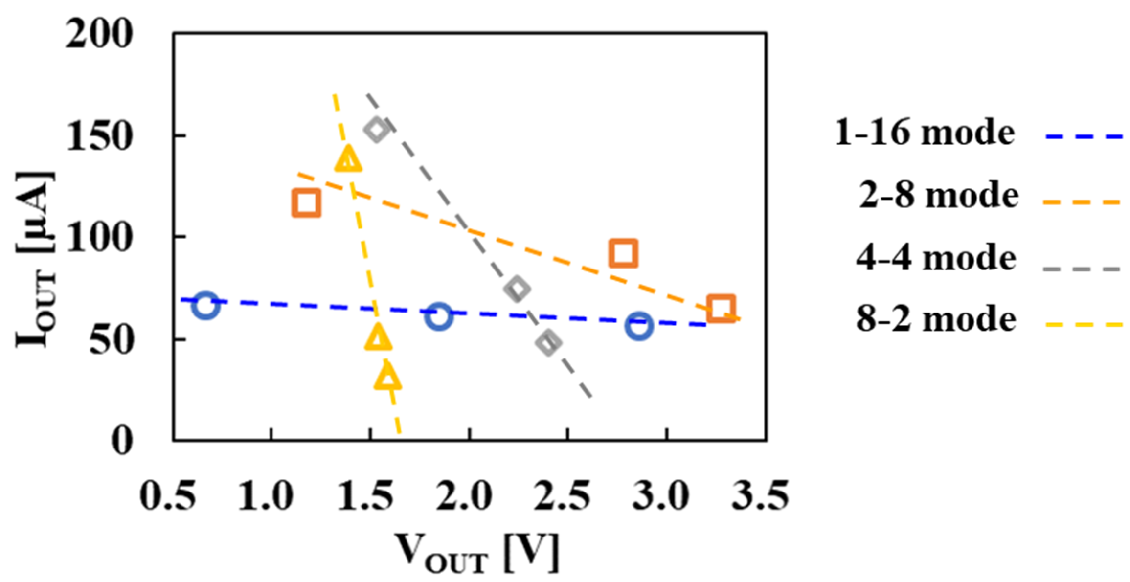
5. Experiment
6. Comparison with Previous Work
7. Summary
Author Contributions
Funding
Institutional Review Board Statement
Informed Consent Statement
Data Availability Statement
Conflicts of Interest
References
- Zanella, A.; Bui, N.; Castellani, A.; Vangelista, L.; Zorzi, M. Internet of Things for Smart Cities. IEEE Internet Things J. 2014, 1, 22–32. [Google Scholar] [CrossRef]
- Al-Fuqaha, A.; Guizani, M.; Mohammadi, M.; Aledhari, M.; Ayyash, M. Internet of Things: A Survey on Enabling Technologies, Protocols, and Applications. IEEE Commun. Surv. Tutorials 2015, 17, 2347–2376. [Google Scholar] [CrossRef]
- Mitcheson, P.D.; Yeatman, E.M.; Rao, G.K.; Holmes, A.S.; Green, T.C. Energy Harvesting from Human and Machine Motion for Wireless Electronic Devices. Proc. IEEE 2008, 96, 1457–1486. [Google Scholar] [CrossRef] [Green Version]
- Sudevalayam, S.; Kulkarni, P. Energy Harvesting Sensor Nodes: Survey and Implications. IEEE Commun. Surv. Tutorials 2010, 13, 443–461. [Google Scholar] [CrossRef] [Green Version]
- Huesgen, T.; Woias, P.; Kockmann, N. Design and fabrication of MEMS thermoelectric generators with high temperature efficiency. Sens. Actuators A Phys. 2008, 145, 423–429. [Google Scholar] [CrossRef]
- Date Sheet of TGP-651, Micropelt. Available online: http://www.micropelt.com/ (accessed on 15 February 2023).
- Du, Y.; Xu, J.; Paul, B.; Eklund, P. Flexible thermoelectric materials and devices. Appl. Mater. Today 2018, 12, 366–388. [Google Scholar] [CrossRef]
- Garofalo, E.; Bevione, M.; Cecchini, L.; Mattiussi, F.; Chiolerio, A. Waste heat to power: Technologies, current applications, and future potential. Energy Technol. 2020, 8, 2000413. [Google Scholar] [CrossRef]
- Nozariasbmarz, A.; Collins, H.; Dsouza, K.; Polash, M.H.; Hosseini, M.; Hyland, M.; Liu, J.; Malhotra, A.; Ortiz, F.M.; Mohaddes, F.; et al. Review of wearable thermoelectric energy harvesting: From body temperature to electronic systems. Appl. Energy 2020, 258, 114069. [Google Scholar] [CrossRef]
- Dickson, J.F. On-Chip High-Voltage Generation in MNOS Integrated Circuits Using an Improved Multiplier Technique. IEEE J. Solid-State Circuits 1976, 11, 374–378. [Google Scholar] [CrossRef]
- Koketsu, K.; Tanzawa, T. A Design of Cold Start Charge Pump for Flexible Thermoelectric Generator with High Output Impedance. In Proceedings of the 2020 27th IEEE International Conference on Electronics, Circuits and Systems, Glasgow, UK, 23–25 November 2020. [Google Scholar] [CrossRef]
- Koketsu, K.; Tanzawa, T. Design of a charge pump circuit and system with input impedance modulation for a flexible-type thermoelectric generator with high-output impedance. Electronics 2021, 10, 1212. [Google Scholar] [CrossRef]
- Xiaosen, L.; Sanchez-Sinencio, E. A 0.45-to-3V reconfigurable charge-pump energy harvester with two-dimensional MPPT for Internet of Things. In Proceedings of the 2015 IEEE International Solid-State Circuits Conference-(ISSCC) Digest of Technical Papers, San Francisco, CA, USA, 22–26 February 2015; pp. 1–3. [Google Scholar]
- Carreon-Bautista, S.; Huang, L.; Sanchez-Sinencio, E. An autonomous energy harvesting power management unit with digital regulation for IoT applications. IEEE J. Solid-State Circuits 2016, 51, 1457–1474. [Google Scholar] [CrossRef]
- Yoon, S.; Carreon-Bautista, S.; Sánchez-Sinencio, E. An Area Efficient Thermal Energy Harvester with Reconfigurable Capacitor Charge Pump for IoT Applications. IEEE Trans. Circuits Syst.—II Express Briefs 2018, 65, 1974–1978. [Google Scholar] [CrossRef] [Green Version]
- Umezawa, A.; Atsumi, S.; Kuriyama, M.; Banba, H.; Imamiya, K.; Naruke, K.; Yamada, S.; Obi, E.; Oshikiri, M.; Suzuki, T.; et al. A 5-V-only operation 0.6- mu m flash EEPROM with row decoder scheme in triple-well structure. IEEE J. Solid-State Circuits 1992, 27, 1540–1546. [Google Scholar] [CrossRef]
- Gariboldi, R.; Pulvirenti, F. A 70 mΩ Intelligent High Side Switch with Full Diagnostics. IEEE J. Solid-State Circuits 1996, 31, 915–923. [Google Scholar] [CrossRef]
- Levacq, D.; Liber, C.; Dessard, V.; Flandre, D. Composite ULP diode fabrication, modelling and applications in multi-Vth FD SOI CMOS technology. Solid-State Electron. 2004, 48, 1017–1025. [Google Scholar] [CrossRef]
- Lian, W.X.; Yong, J.K.; Chong, G.; Churchill, K.K.P.; Ramiah, H.; Chen, Y.; Mak, P.-I.; Martins, R.P. A Reconfigurable Hybrid RF Front-End Rectifier for Dynamic PCE Enhancement of Ambient RF Energy Harvesting Systems. Electronics 2023, 12, 175. [Google Scholar] [CrossRef]
- Tanzawa, T.; Tanaka, Y.; Tanaka, T.; Nakamura, H.; Oodaira, H.; Sakui, K.; Momodomi, M.; Shiratake, S.; Nakano, H.; Oowaki, Y.; et al. A quick boosting charge pump circuit for high density and low voltage flash memories. In Proceedings of the 1994 IEEE Symposium on VLSI Circuits, San Diego, CA, USA, 9–11 June 1994; pp. 65–66. [Google Scholar]
- Tanzawa, T.; Tanaka, T.; Takeuchi, K.; Nakamura, H. Circuit Techniques for a 1.8-V-Only NAND Flash Memory. IEEE J. Solid-State Circuits 2002, 37, 84–89. [Google Scholar] [CrossRef]
- Tanzawa, T. Design of DC-DC Switched-Capacitor Voltage Multiplier driven by DC Energy Transducer. In Proceedings of the IEEE International Conference on Electronics, Circuits and Systems, Marseille, France, 7–10 December 2014; pp. 327–330. [Google Scholar]
- Suemori, K.; Hoshino, S.; Kamata, T. Flexible and lightweight thermoelectric generators composed of carbon nanotube–polystyrene composites printed on film substrate. Appl. Phys. Lett. 2013, 103, 153902. [Google Scholar] [CrossRef]
- Tanzawa, T. A Switch-Resistance-Aware Dickson Charge Pump Model for Optimizing Clock Frequency. IEEE Trans. Circuits Syst. II Express Briefs 2011, 58, 336–340. [Google Scholar] [CrossRef]
- Nono, K.; Tanzawa, T. A Design of Adaptive Charge Pumps with Minimum Circuit Area for Thermoelectric Energy Harvesting under Temperature Variations. IEICE General Conference, C-12-27, March 2021. Available online: http://hdl.handle.net/10297/00027950 (accessed on 15 February 2023).
- Nono, K.; Tanzawa, T. A Design of Charge Pump System with Maximum Power Point Tracking for Low Cost Thermoelectric Energy Harvesting, IEICE Society Conference, C-12-3, September 2021. Available online: http://hdl.handle.net/10297/00028355 (accessed on 15 February 2023).


| Parameter | Definition | Default Value | |
|---|---|---|---|
| TEG | VOC | Open-circuit voltage as a function of temperature gradient | 0.5, 0.7, 1.0, 1.5, 2.0 V |
| RS | Output resistance | 600 Ω | |
| CP | C | Stage capacitance | TBD |
| N | Number of stage capacitors | TBD | |
| f | Clock frequency | 10 MHz | |
| VPP | Target output voltage | 3.0 V | |
| VT | Effective thermal voltage of charge transfer switches (CTS) | 26 mV | |
| ISAT | Saturation current of CTS | 40 nA | |
| αT | Ratio of top plate capacitance to C | 0.05 | |
| αB | Ratio of bottom plate capacitance to C | 0.1 |
| Liu, 2015 [13] | Bautista, 2016 [14] | Yoon, 2018 [15] | This Work | |||
|---|---|---|---|---|---|---|
| Technology [nm] | 180 | 180 | 130 | 65 | ||
| Energy transducer | TEG/PV (*1) | TEG/PV/MFC (*1) | TEG | TEG | ||
| Operation range of VS [V] | 1.28~3.0 | 0.25~1.1 | 0.27~1.0 | 0.34~1.2 (VOC = 0.5~2.0 V) | ||
| Target output voltage VPP_TGT [V] | 3.3 | 1.8 | 1.0 | 3.0 | ||
| MPPT | Procedure | Two steps in order | Two steps in parallel | Two steps in order | Single step | |
| Parameters to be measured | ΔVPP, i.e., IPP | VS~VMPPT | VPP~VPP_TGT | (1) VS~VMPPT, (2) VPP~VPP_TGT | VOC | |
| Parameters to be updated | (1) N, (2) f | f | N | (1) Combination of C, N, (2) f | Combination of C, N | |
| Parameter to be maximized | POUT | PIN | PIN | POUT | ||
| Area [mm2] | 1.03 | 2.82 | 0.835 | 0.302 (*2) | ||
| Maximum power efficiency of CP [%] | 79 (TEG) 89 (PV) | 57 | 64 | 67 | ||
| Maximum output power POUT_MAX [mW] | 0.04 | 1.62 | 0.40 | 1.11 | ||
| POUT_MAX/Area [mW/mm2] | 0.04 | 0.57 | 0.48 | 3.66 (*2) | ||
Disclaimer/Publisher’s Note: The statements, opinions and data contained in all publications are solely those of the individual author(s) and contributor(s) and not of MDPI and/or the editor(s). MDPI and/or the editor(s) disclaim responsibility for any injury to people or property resulting from any ideas, methods, instructions or products referred to in the content. |
© 2023 by the authors. Licensee MDPI, Basel, Switzerland. This article is an open access article distributed under the terms and conditions of the Creative Commons Attribution (CC BY) license (https://creativecommons.org/licenses/by/4.0/).
Share and Cite
Nono, K.; Tanzawa, T. One-Dimensional Maximum Power Point Tracking Design of Switched-Capacitor Charge Pumps for Thermoelectric Energy Harvesting. Electronics 2023, 12, 1203. https://doi.org/10.3390/electronics12051203
Nono K, Tanzawa T. One-Dimensional Maximum Power Point Tracking Design of Switched-Capacitor Charge Pumps for Thermoelectric Energy Harvesting. Electronics. 2023; 12(5):1203. https://doi.org/10.3390/electronics12051203
Chicago/Turabian StyleNono, Koichi, and Toru Tanzawa. 2023. "One-Dimensional Maximum Power Point Tracking Design of Switched-Capacitor Charge Pumps for Thermoelectric Energy Harvesting" Electronics 12, no. 5: 1203. https://doi.org/10.3390/electronics12051203