
Experimental Validation of a Bidirectional Multilevel dc–dc Power Converter for Electric Vehicle Battery Charging Operating under Normal and Fault Conditions


Abstract
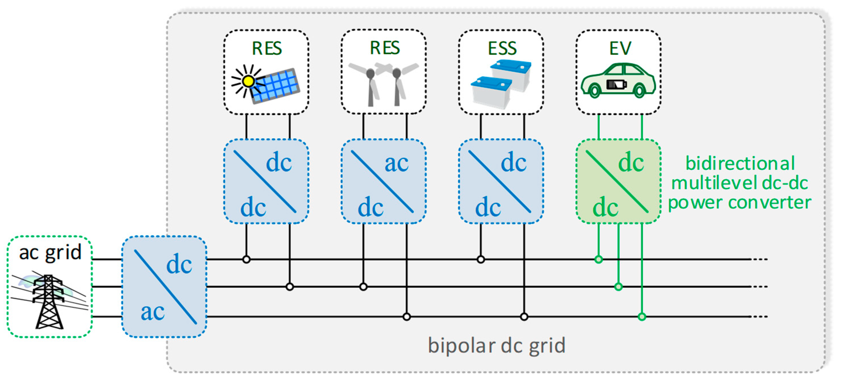
:1. Introduction
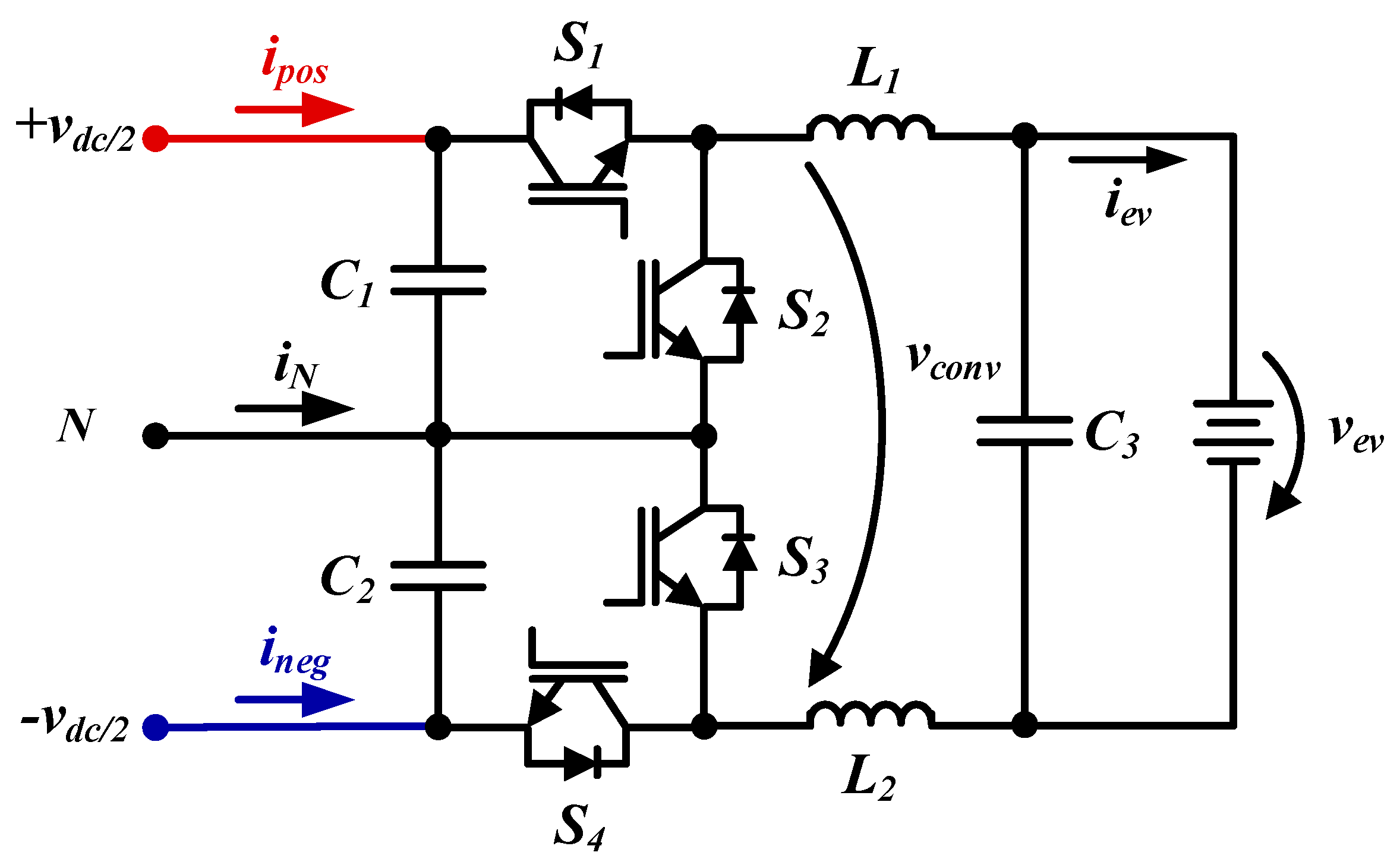
2. Description of the Multilevel dc–dc Power Converter
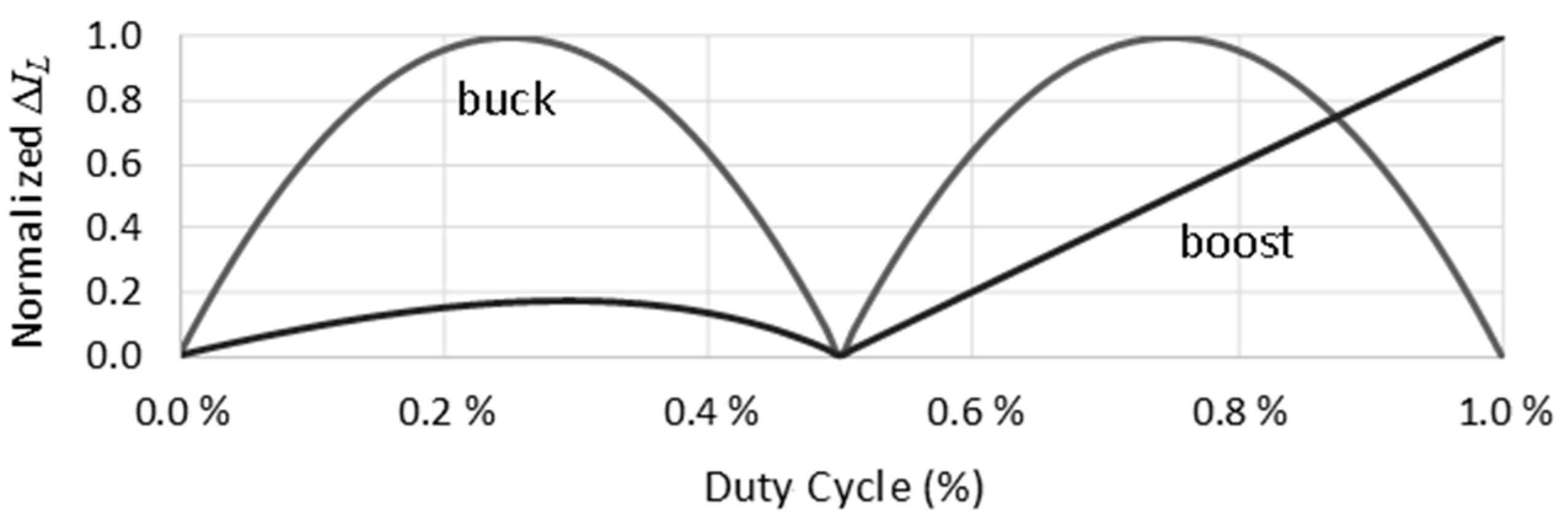
2.1. Multilevel dc–dc Power Converter Operation under Normal Conditions
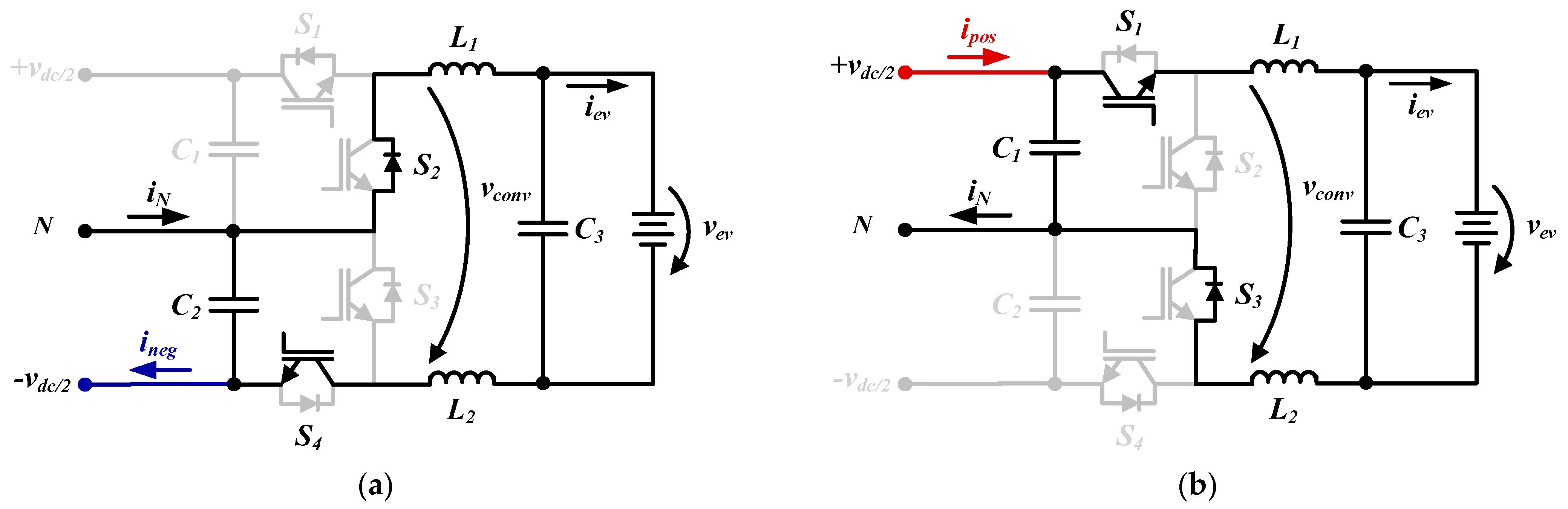
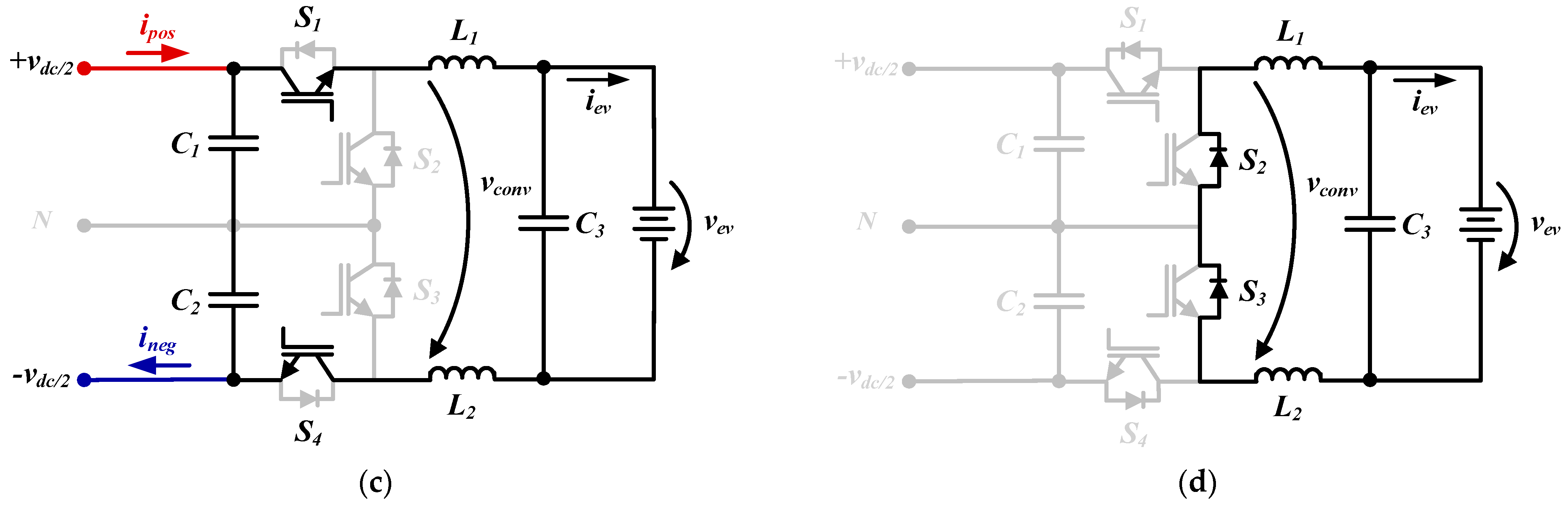
2.2. Multilevel dc–dc Power Converter Operation under Fault Conditions
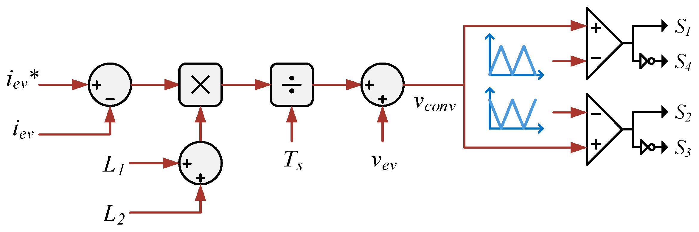
2.3. Operation Principle of the Control Strategy Applied in Normal and Fault Conditions
3. Computational Validation
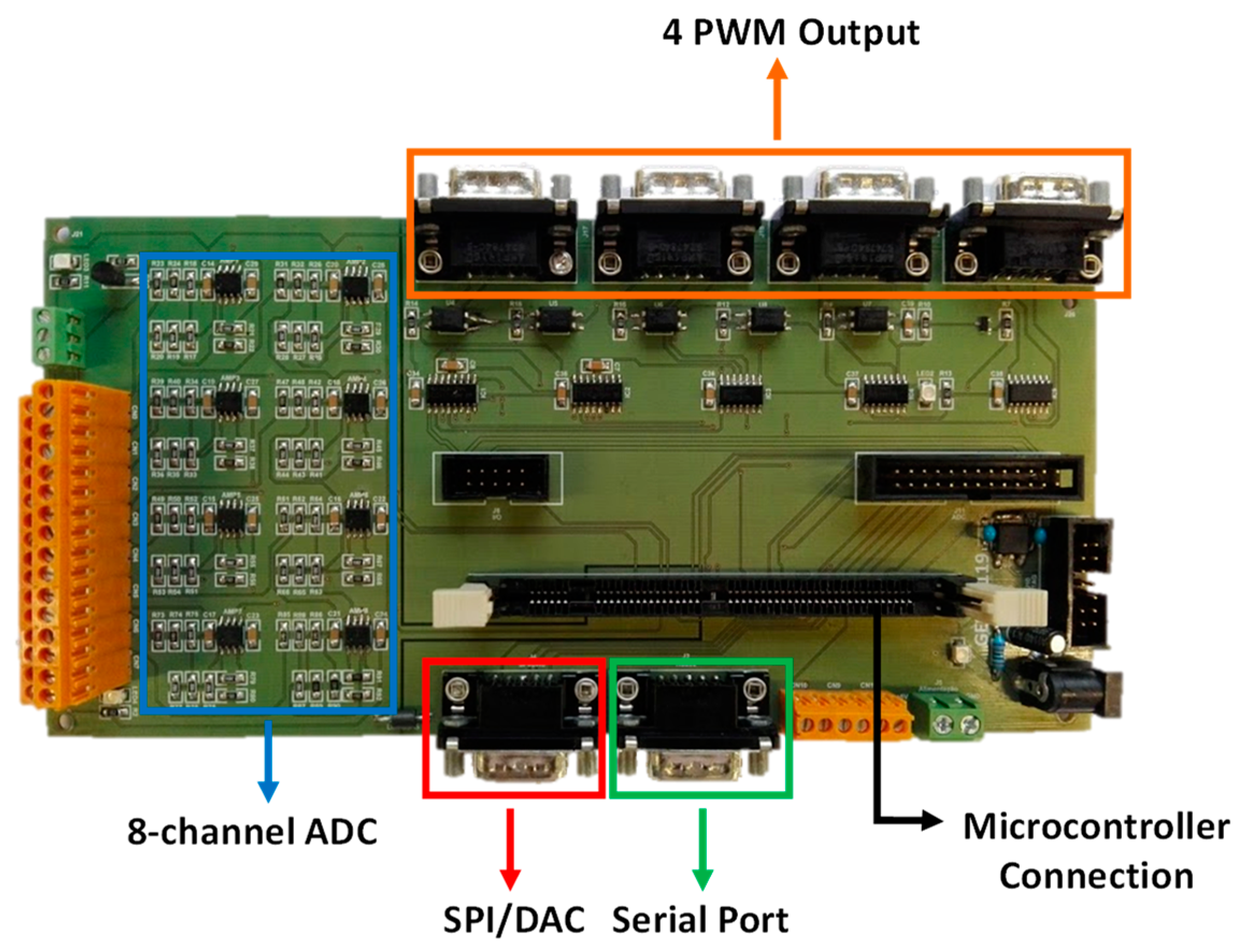
4. Experimental Validation
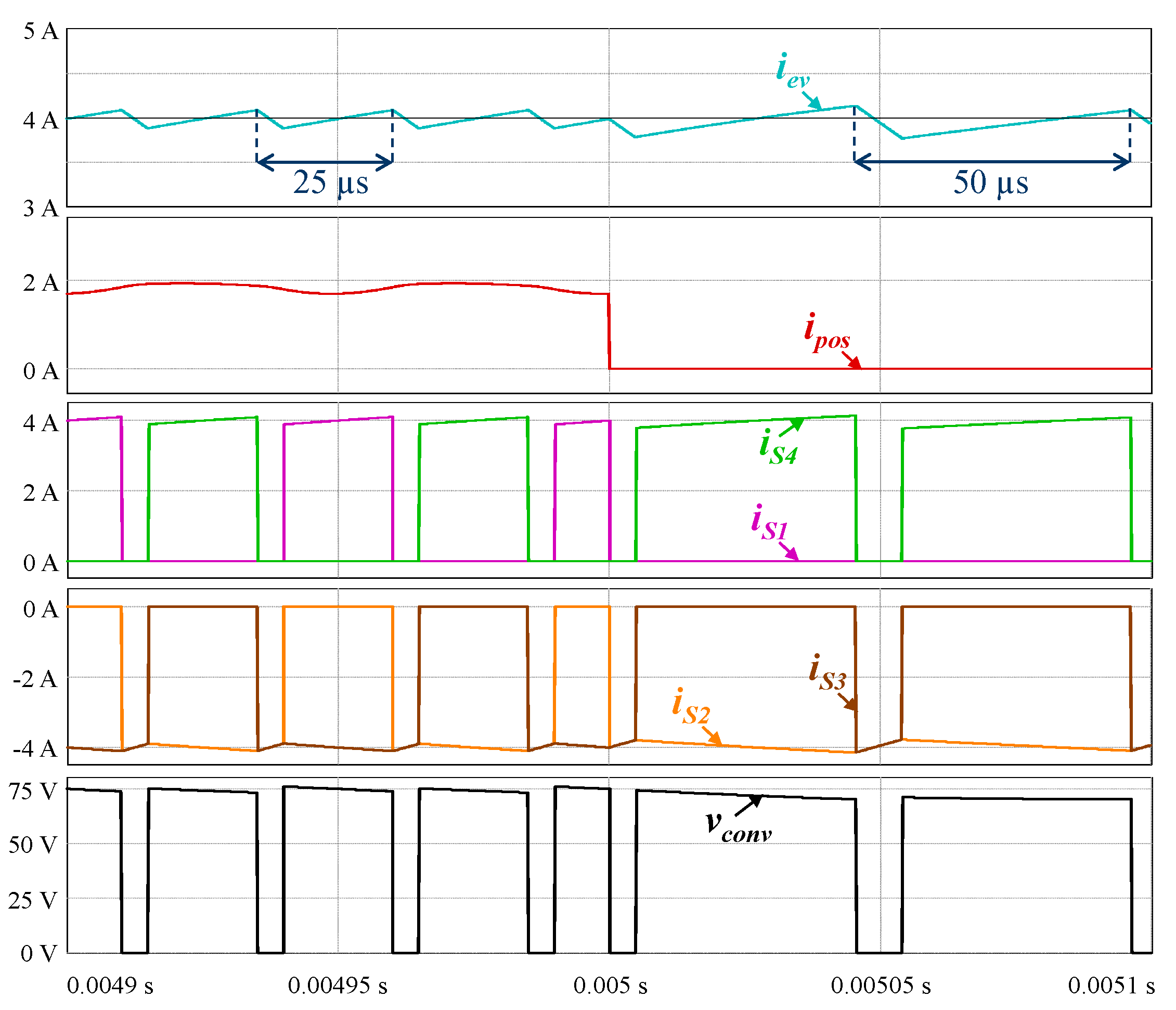
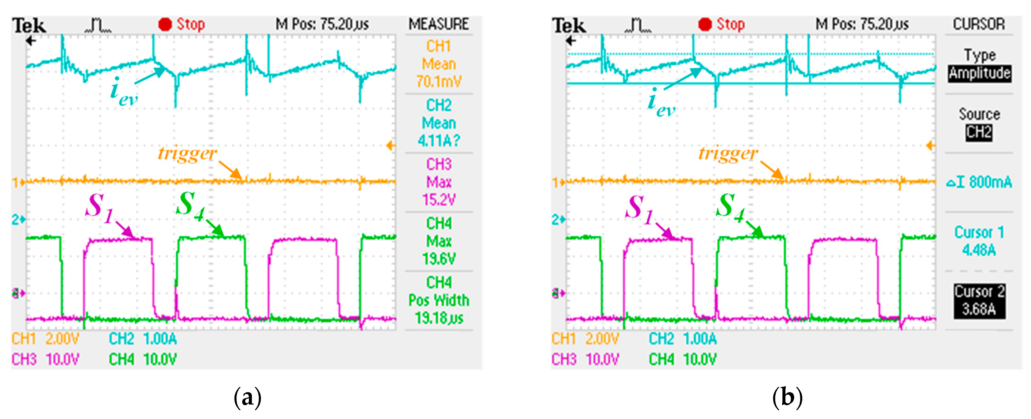
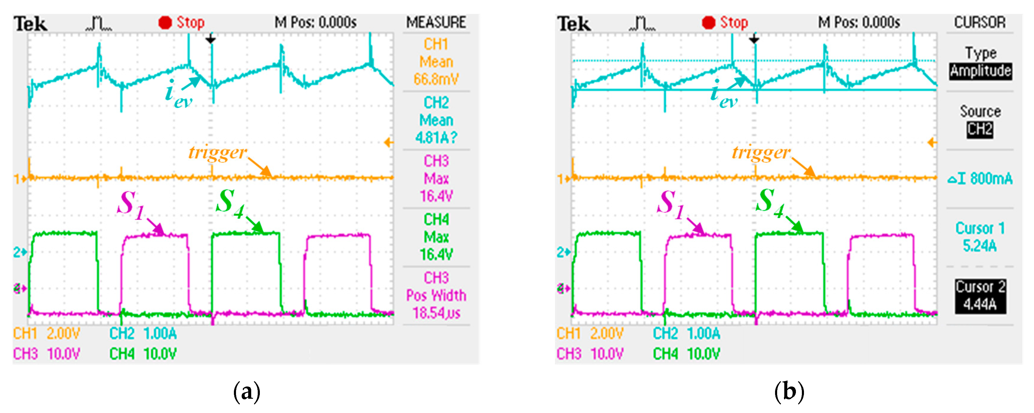
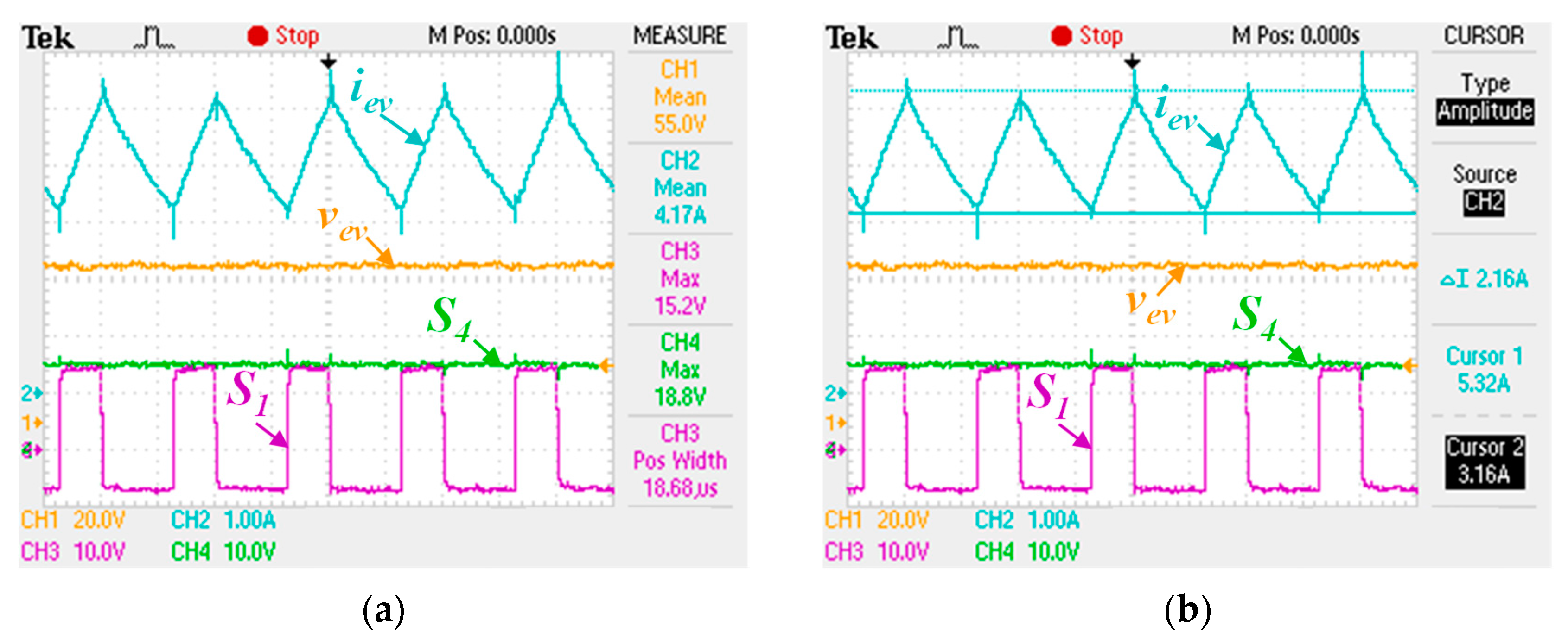
4.1. Operation under Normal Conditions
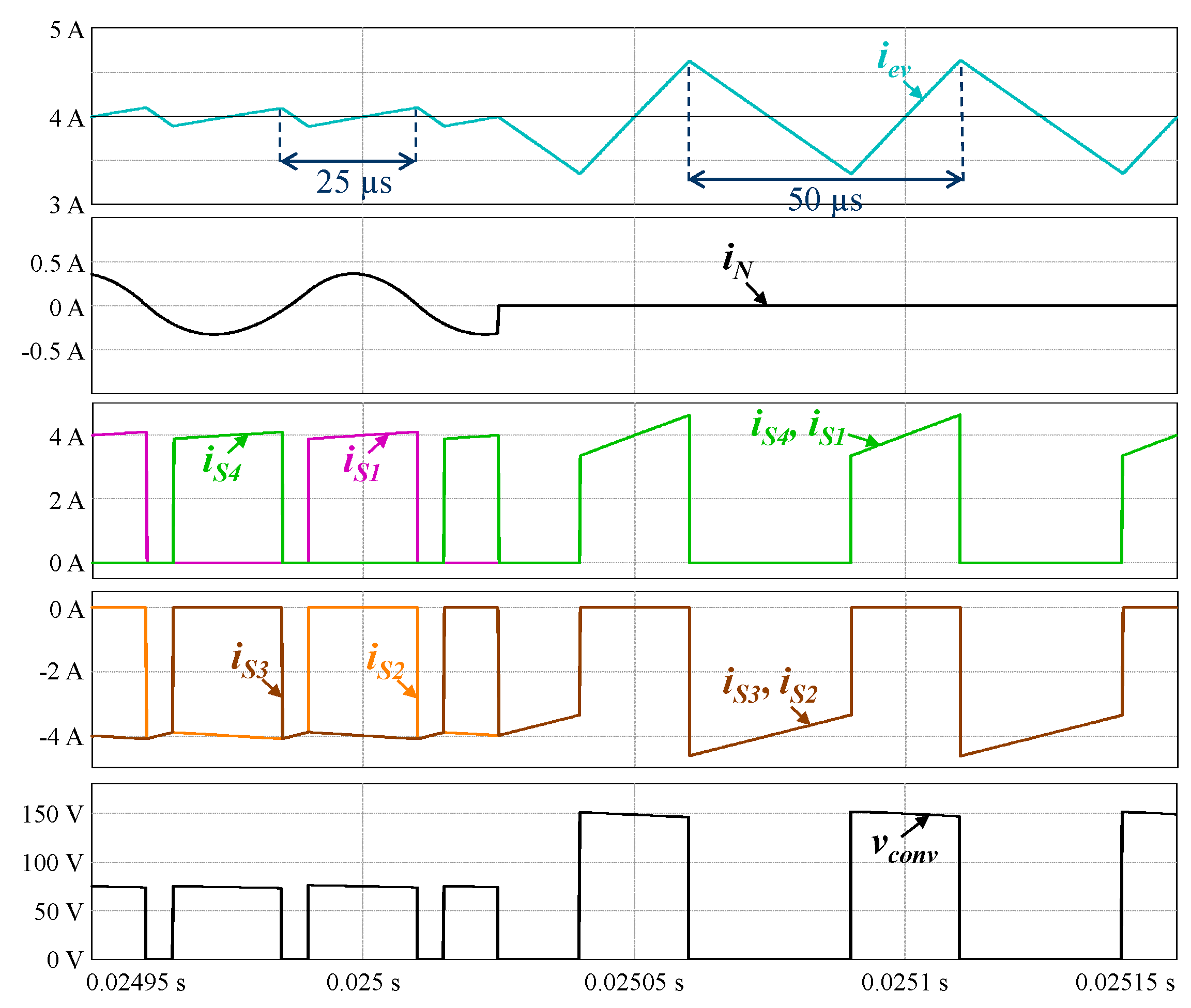
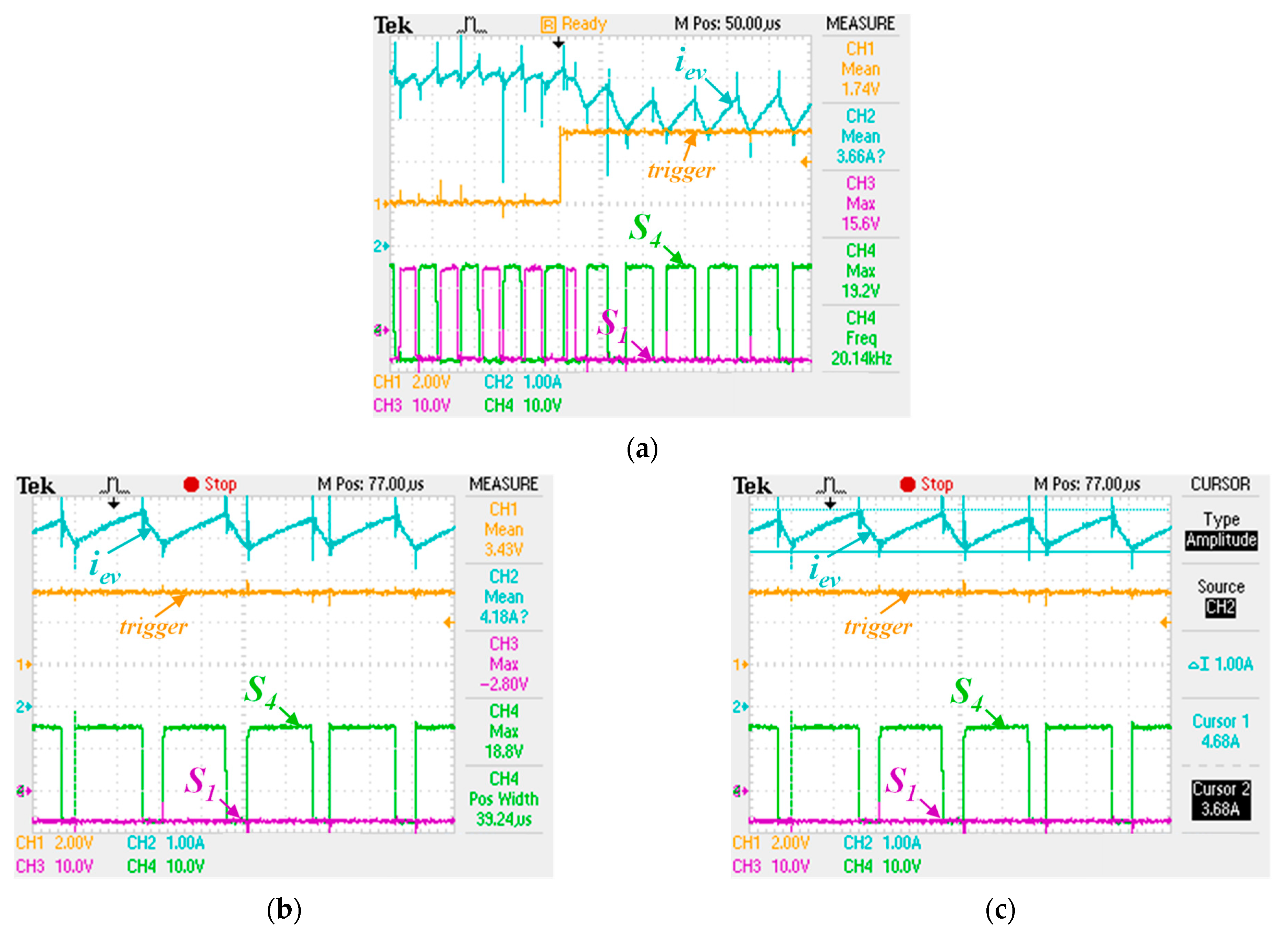
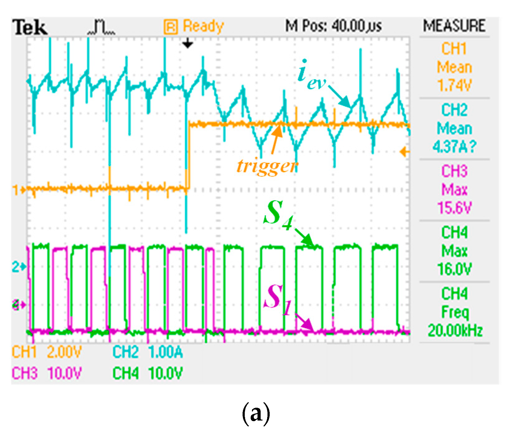
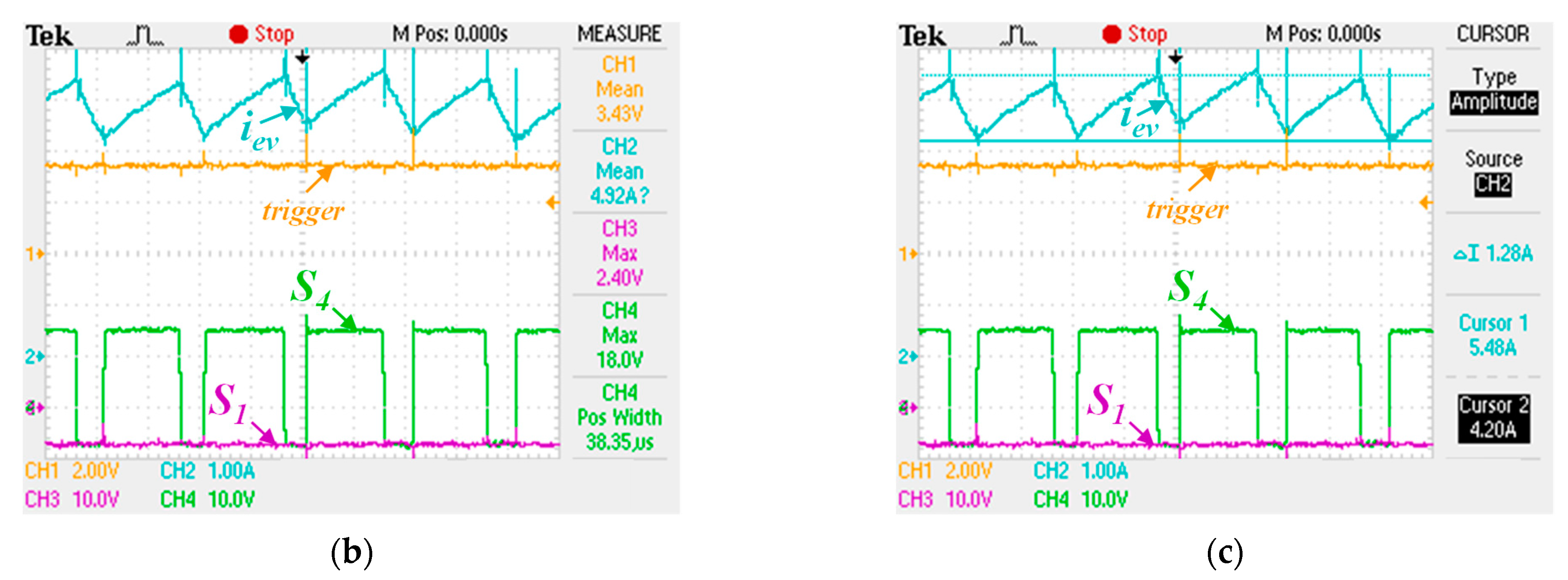
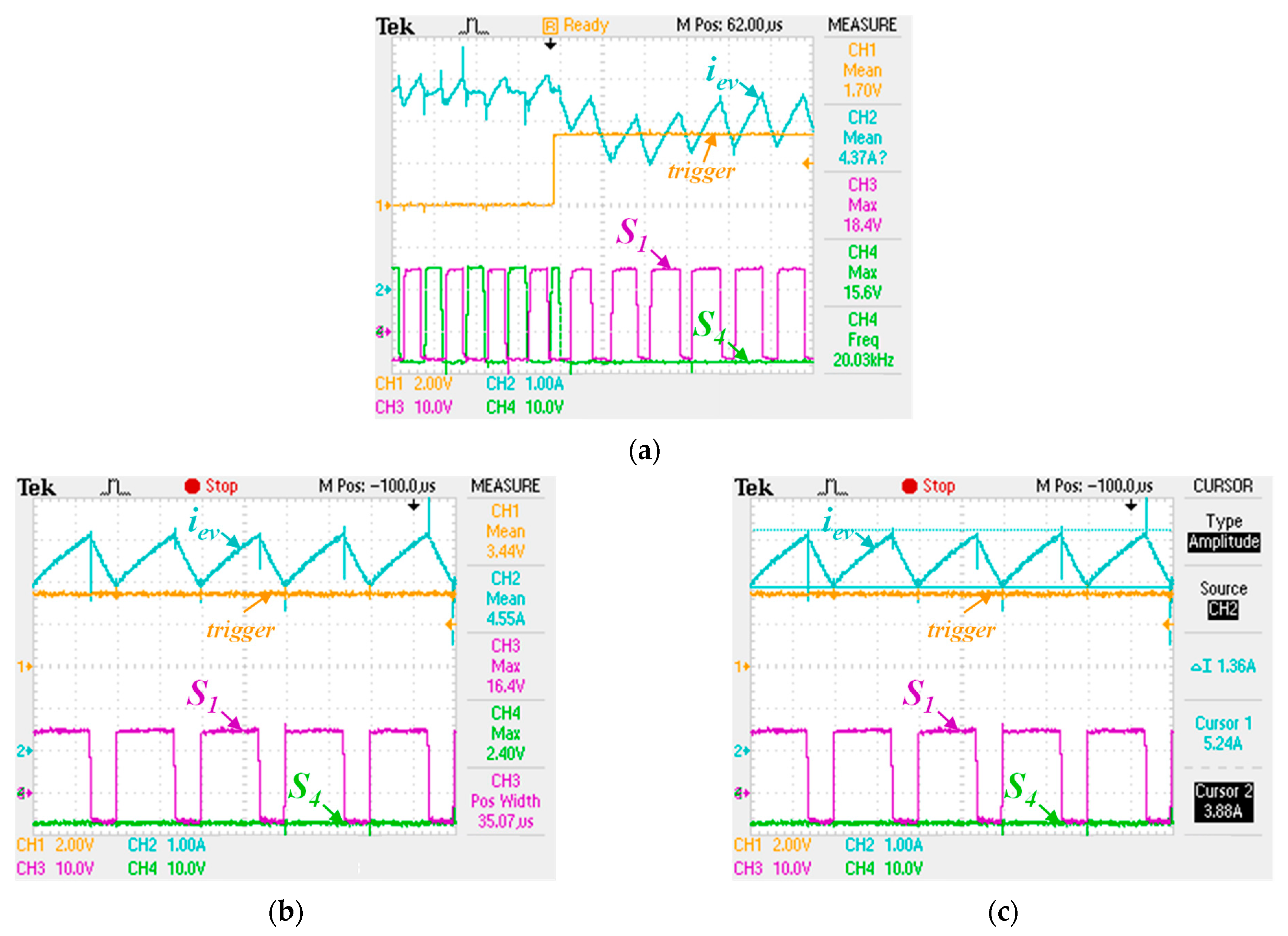
4.2. Operation under Fault Conditions
5. Conclusions
Author Contributions
Funding
Conflicts of Interest
References
- Sharma, G.; Sood, V.; Alam, M.; Shariff, S. Comparison of common DC and AC bus architectures for EV fast charging stations and impact on power quality. ETransportation 2020, 5, 100066. [Google Scholar]
- Leone, C.; Longo, M.; Fernández-Ramírez, L.M. Optimal Size of a Smart Ultra-Fast Charging Station. Electronics 2021, 10, 2887. [Google Scholar]
- Monteiro, V.; Afonso, J. A Unified Topology for the Integration of Electric Vehicle, Renewable Energy Source, and Active Filtering for the Power Quality Improvement of the Electrical Power Grid: An Experimental Validation. Electronics 2022, 11, 429. [Google Scholar]
- Montoya, O.; Garrido, V.; Gil-González, W.; Grisales-Noreña, L. Power flow analysis in DC grids: Two alternative numerical methods. Trans. Circuits Syst. II Express Briefs 2019, 66, 1865–1869. [Google Scholar]
- Jiya, I.; Khang, H.; Kishor, N.; Ciric, R. Novel Family of High-Gain Nonisolated Multiport Converters with Bipolar Symmetric Outputs for DC Microgrids. Trans. Power Electron. 2022, 37, 12151–12166. [Google Scholar] [CrossRef]
- Chandra, A.; Singh, G.; Pant, V. Protection techniques for DC microgrid- A review. Electr. Power Syst. Res. 2020, 187, 106439. [Google Scholar]
- Zhao, S.; Chen, Y.; Cui, S.; Hu, J. Modular Multilevel DC-DC Converter With Inherent Bipolar Operation Capability for Resilient Bipolar MVDC Grids. CPSS Trans. Power Electron. Appl. 2022, 7, 37–48. [Google Scholar] [CrossRef]
- Jarrahi, M.; Roozitalab, F.; Arefi, M.; Javadi, M.; Catalao, J. Dc microgrid energy management system containing photovoltaic sources considering supercapacitor and battery storages. In Proceedings of the 2020 International Conference on Smart Energy Systems and Technologies (SEST), Istanbul, Turkey, 7–9 September 2020; pp. 1–6. [Google Scholar]
- Metwly, M.; Abdel-Majeed, M.; Abdel-Khalik, A.; Hamdy, R.; Hamad, M.; Ahmed, S. A review of integrated on-board EV battery chargers: Advanced topologies, recent developments and optimal selection of FSCW slot/pole combination. Access 2020, 8, 85216–85242. [Google Scholar]
- Monteiro, V.; Lima, P.; Sousa, T.; Martins, J.; Afonso, J. An off-board multi-functional electric vehicle charging station for smart homes: Analysis and experimental validation. Energies 2020, 13, 1864. [Google Scholar] [CrossRef]
- Ali, A.; Chuanwen, J.; Yan, Z.; Habib, S.; Khan, M. An efficient soft-switched vienna rectifier topology for EV battery chargers. Energy Rep. 2021, 7, 5059–5073. [Google Scholar] [CrossRef]
- Monteiro, V.; Pinto, J.; Afonso, J. Improved vehicle-for-grid (iV4G) mode: Novel operation mode for EVs battery chargers in smart grids. Int. J. Electr. Power Energy Syst. 2019, 110, 579–587. [Google Scholar] [CrossRef]
- Schäfer, J.; Kolar, J. Three-Port Series-Resonant DC/DC Converter for Automotive Charging Applications. Electronics 2021, 10, 2543. [Google Scholar]
- Arif, S.; Lie, T.; Seet, B.; Ayyadi, S.; Jensen, K. Review of Electric Vehicle Technologies, Charging Methods, Standards and Optimization Techniques. Electronics 2021, 10, 1910. [Google Scholar]
- Gaona-Cárdenas, L.-F.; Vázquez-Nava, N.; Ruíz-Martínez, O.-F.; Espinosa-Calderón, A.; Barranco-Gutiérrez, A.-I.; Rodríguez-Licea, M.-A. An Overview on Fault Management for Electric Vehicle Onboard Chargers. Electronics 2022, 11, 1107. [Google Scholar] [CrossRef]
- Balasundar, C.; Sundarabalan, S.; Sharma, J.; Srinath, J.; Guerrero, J. Effect of Fault Ride Through Capability on Electric Vehicle Charging Station Under Critical Voltage Conditions. Trans. Transp. Electrif. 2022, 8, 2469–2478. [Google Scholar]
- Bento, F.; Cardoso, A. Fault tolerant DC-DC converters in DC microgrids. In Proceedings of the 2017 IEEE Second International Conference on DC Microgrids (ICDCM), Nuremburg, Germany, 27–29 June 2017; pp. 484–490. [Google Scholar]
- Wen, H.; Li, J.; Shi, H.; Hu, Y.; Yang, Y. Fault Diagnosis and Tolerant Control of Dual-Active-Bridge Converter with Triple-Phase Shift Control for Bidirectional EV Charging Systems. Trans. Transp. Electrif. 2021, 7, 287–303. [Google Scholar]
- Kaler, S.; Yazdani, A. A DC-Side Fault-Tolerant Bidirectional AC-DC Converter for Applications in Distribution Systems. Access 2022, 10, 46608–46617. [Google Scholar]
- Wang, Y.; Guan, Y.; Molinas, M.; Fosso, O.; Hu, W.; Zhang, Y. Open-Circuit Switching Fault Analysis and Tolerant Strategy for Dual-Active-Bridge DC–DC Converter Considering Parasitic Parameters. Trans. Power Electron. 2022, 37, 15020–15034. [Google Scholar] [CrossRef]
- Caseiro, L.; Mendes, A. Fault Analysis and Non-Redundant Fault Tolerance in 3-Level Double Conversion UPS Systems Using Finite-Control-Set Model Predictive Control. Energies 2021, 14, 2210. [Google Scholar]
- Kumar, G.; Elangovan, D. Review on fault-diagnosis and fault-tolerance for DC-DC converters. Power Electron. 2020, 13, 1–13. [Google Scholar]
- Bhargav, R.; Bhalja, B.; Gupta, C. Novel fault detection and localization algorithm for low-voltage dc microgrid. Trans. Ind. Inform. 2019, 16, 4498–4511. [Google Scholar]
- Zhuo, S.; Xu, L.; Gaillard, A.; Huangfu, Y.; Paire, D.; Gao, F. Robust open-circuit fault diagnosis of multi-phase floating interleaved DC-DC boost converter based on sliding mode observer. Trans. Transp. Electrif. 2019, 5, 638–649. [Google Scholar] [CrossRef]
- Zhuo, S.; Gaillard, A.; Xu, L.; Liu, C.; Paire, D.; Gao, F. An Observer-Based Switch Open-Circuit Fault Diagnosis of DC–DC Converter for Fuel Cell Application. Trans. Ind. Appl. 2020, 56, 3159–3167. [Google Scholar]
- Givi, H.; Farjah, E.; Ghanbari, T. Switch and Diode Fault Diagnosis in Nonisolated DC–DC Converters Using Diode Voltage Signature. Trans. Ind. Electron. 2018, 65, 1606–1615. [Google Scholar] [CrossRef]
- Xu, L.; Ma, R.; Xie, R.; Xu, J.; Huangfu, Y.; Gao, F. Open-Circuit Switch Fault Diagnosis and Fault-Tolerant Control for Output-Series Interleaved Boost DC-DC Converter. Trans. Transp. Electrif. 2021, 7, 2054–2066. [Google Scholar]
- Bento, F.; Cardoso, A. Open-circuit fault diagnosis and fault tolerant operation of interleaved DC-DC boost converters for homes and offices. Trans. Ind. Appl. 2019, 55, 4855–4864. [Google Scholar] [CrossRef]
- Leite, R.; Afonso, J.; Monteiro, V. A novel multilevel bidirectional topology for on-board EV battery chargers in smart grids. Energies 2018, 11, 3453. [Google Scholar]


Disclaimer/Publisher’s Note: The statements, opinions and data contained in all publications are solely those of the individual author(s) and contributor(s) and not of MDPI and/or the editor(s). MDPI and/or the editor(s) disclaim responsibility for any injury to people or property resulting from any ideas, methods, instructions or products referred to in the content. |
© 2023 by the authors. Licensee MDPI, Basel, Switzerland. This article is an open access article distributed under the terms and conditions of the Creative Commons Attribution (CC BY) license (https://creativecommons.org/licenses/by/4.0/).
Share and Cite
Monteiro, V.; Oliveira, C.F.; Afonso, J.L. Experimental Validation of a Bidirectional Multilevel dc–dc Power Converter for Electric Vehicle Battery Charging Operating under Normal and Fault Conditions. Electronics 2023, 12, 851. https://doi.org/10.3390/electronics12040851
Monteiro V, Oliveira CF, Afonso JL. Experimental Validation of a Bidirectional Multilevel dc–dc Power Converter for Electric Vehicle Battery Charging Operating under Normal and Fault Conditions. Electronics. 2023; 12(4):851. https://doi.org/10.3390/electronics12040851
Chicago/Turabian StyleMonteiro, Vitor, Catia F. Oliveira, and Joao L. Afonso. 2023. "Experimental Validation of a Bidirectional Multilevel dc–dc Power Converter for Electric Vehicle Battery Charging Operating under Normal and Fault Conditions" Electronics 12, no. 4: 851. https://doi.org/10.3390/electronics12040851