
Low-Power Regulated Cascode CMOS Transimpedance Amplifier with Local Feedback Circuit
by
 , ,
, ,
Yasuhiro Takahashi
1,* ,
,
Daisuke Ito
1 ,
,
Makoto Nakamura
1,
Akira Tsuchiya
2,
Toshiyuki Inoue
2 and
Keiji Kishine
2 1
Department of Electrical, Electronic and Computer Engineering, Faculty of Engineering, Gifu University, 1-1 Yanagido, Gifu 501-1193, Japan
2
Department of Electronic Systems Engineering, School of Engineering, The University of Shiga Prefecture, 2500 Yasakamachi, Hikone-shi 522-0057, Japan
*
Author to whom correspondence should be addressed.
Electronics 2022, 11(6), 854; https://doi.org/10.3390/electronics11060854
Submission received: 7 February 2022
/
Revised: 4 March 2022
/
Accepted: 8 March 2022
/
Published: 9 March 2022
(This article belongs to the Topic Fiber Optic Communication)
Abstract
:In this paper, we propose a multistage transimpedance amplifier (TIA) based on the local negative feedback technique. Compared with the conventional global-feedback technique, the proposed TIA has the advantages of a wider bandwidth, and lower power dissipation. The schematic and characteristics of the proposed TIA circuit are described. Moreover, the proposed TIA employs inductive peaking to increase bandwidth. The TIA is implemented using a 65 nm complementary metal oxide semiconductor (CMOS) technology and consumes 23.9 mW with a supply voltage of 1.0 V. Using a back-annotated simulation, we obtained the following characteristics: a gain of 46 dB and −3 dB frequency of 11.4 GHz. TIA occupies an area of 366 m × 225 m.
1. Introduction
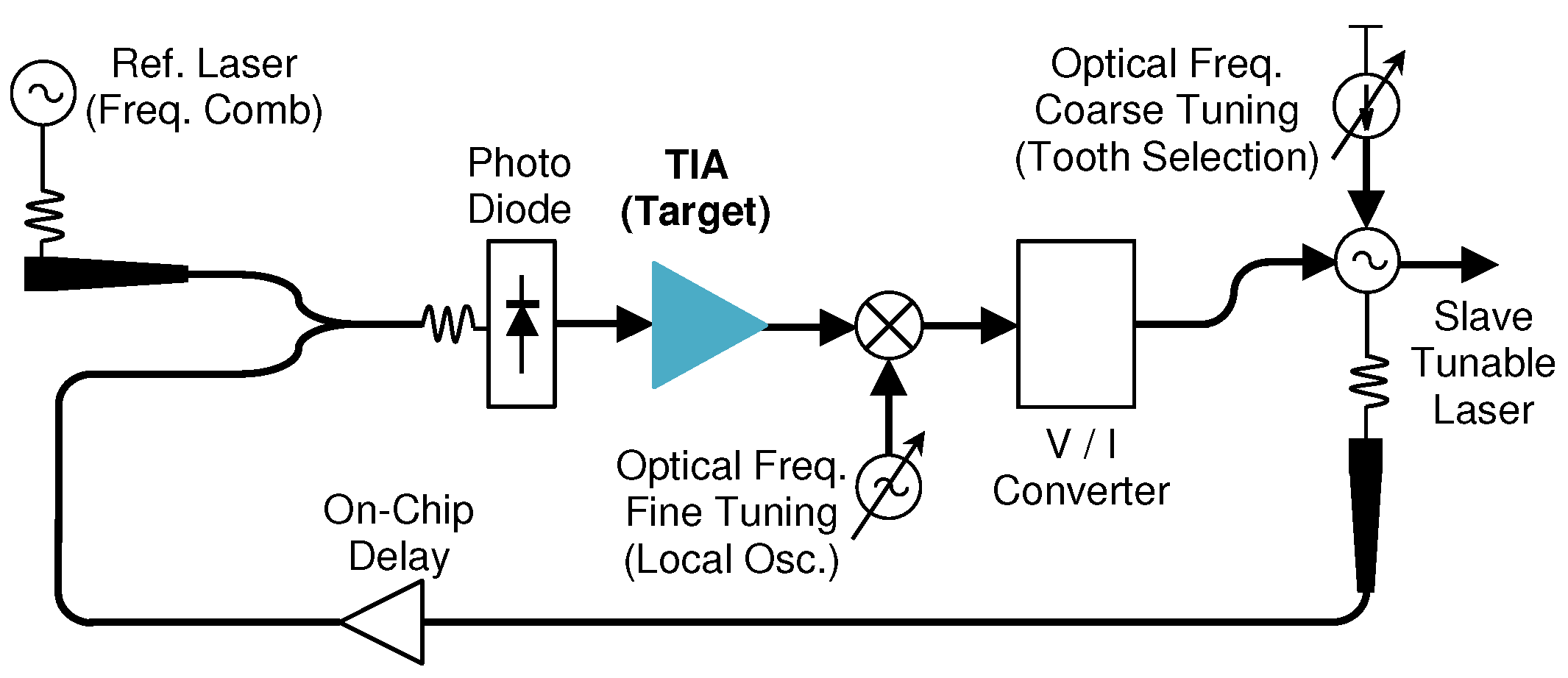
A transimpedance amplifier (TIA) is a very important building block for current optoelectronic communication systems, e.g., optical receivers for optical frequency combs [1,2,3], localized machine-to-machine (i.e., short distance) communication systems [4,5], or optical metro long-haul fiber communication systems [6,7,8]. The TIA is one of the most important components of optical receivers. Figure 1 shows the conceptual block diagram of an integrated optical heterodyne receiver [9]. For optical heterodyne receiver systems, we are confronted with a new problem of extending the bandwidth of the TIA, as well as the photodiode (PD) to maximize the range of synthesizable frequencies. TIAs can be fabricated using many different transistor processes, but CMOS process offers the ability of direct integration with digital logic circuits. This integration is vital, as the challenges encountered by optical heterodyne receivers include cost (e.g., chip size and power consumption). In [2,3], Costanzo proposed a current reuse regulated cascode (RGC) CMOS TIA; they then fabricated and measured it, but the proposed TIAs still had a high-power consumption.
In [8], to extend the frequency response, we proposed multiple shunt–shunt feedback (i.e., overall feedback) and fabricated it using a 0.25 m InP heterojunction bipolar transistor (HBT) process. The proposed TIA was designed for long-haul fiber communications using the InP HBT process; hence, when designing a complete optical receiver system, a digital part of the chip, such as field-programmable gate array or application-specific integrated circuit, is needed. This paper proposes an RGC type TIA based on a local feedback technique. Using the modified feedback technique, the frequency band of the proposed TIA is wider than that of our proposed shunt–shunt feedback. In this study, we designed a TIA using a 65 nm CMOS process and simulated it through post-layout. The results obtained were a 46 dB Gain and −3 dB frequency of 11.4 GHz. The remainder of this paper is organized as follows. Section 2 describes the conventional TIA based on the traditional broadband design technique using a multiple shunt–shunt overall feedback, then the proposed TIA based on the modified feedback technique is presented The post-layout simulation results are presented in Section 3 and the conclusions are summarized in Section 4. In Appendix A, the measured 2-port S-parameters of the fabricated TIA is presented, in order to simplify testings.
2. TIA Design
2.1. Conventional TIA Based on Overall Feedback Technique
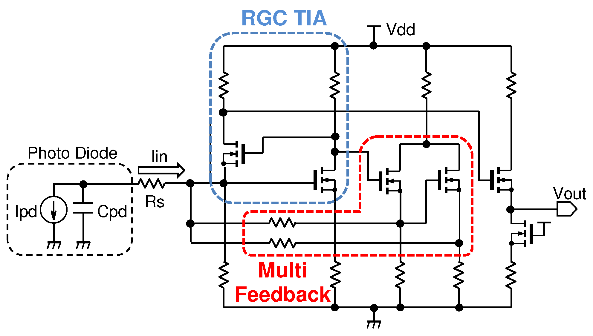
Figure 2 shows a schematic of a conventional RGC TIA based on a feedback technique [8]. The TIA is composed of the following three parts: an RGC input stage (blue dotted line in Figure 2), two feedback-gain stages (red dotted line) and a source follower output stage [10]. Because the input current of the TIA core is divided by the shunt feedback network, the input impedance can be reduced. Therefore, the bandwidth of the proposed circuit is further expanded compared with the conventional simple RGC input stage.
2.2. Proposed TIA
2.2.1. Circuit Structure
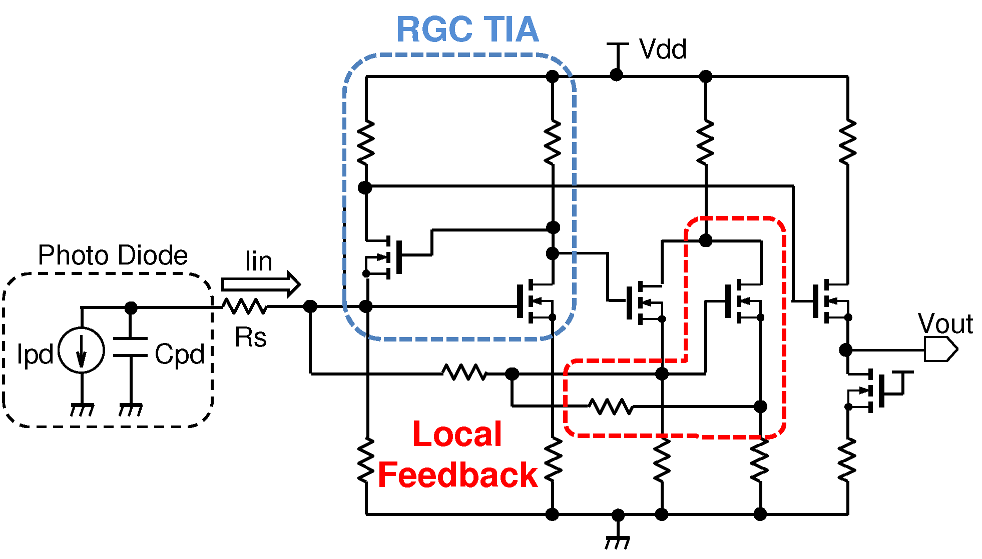
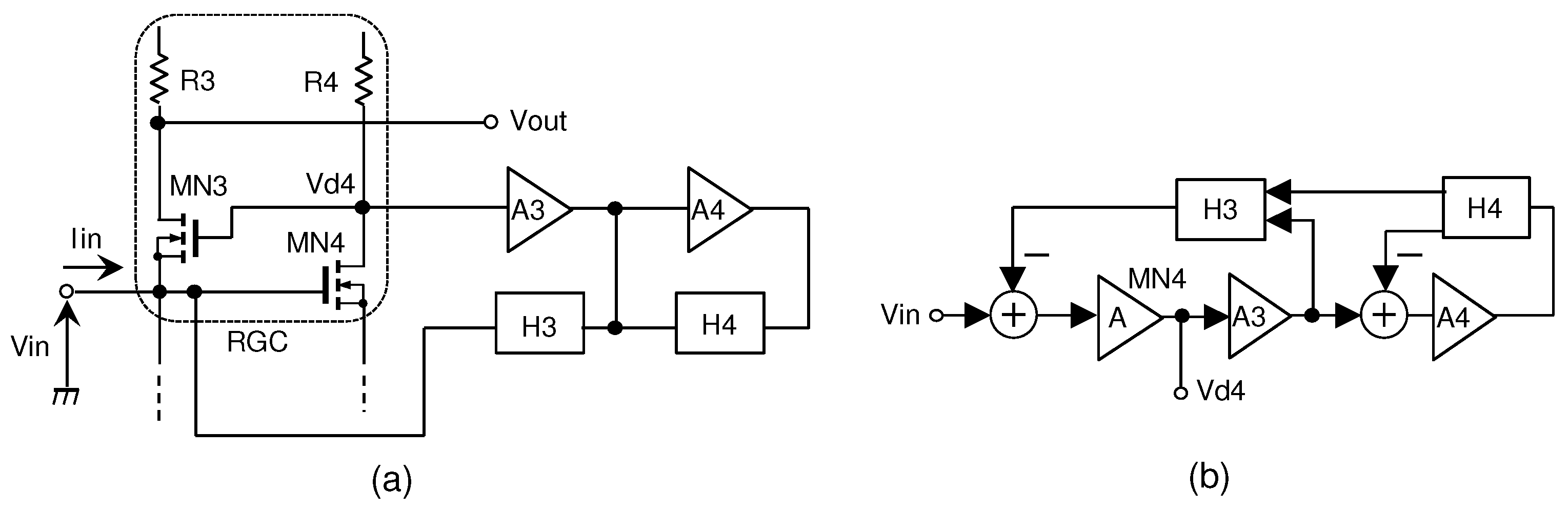
Figure 3 shows the proposed TIA with overall and local feedback stages. Compared with the conventional TIA shown in Figure 2, the second feedback-gain stage of the proposed TIA has a local feedback configuration. The resulting frequency of the proposed TIA is expanded. To understand the circuit mechanism of the conventional and proposed TIA, we analyze their transfer functions in Section 2.2.2.
2.2.2. Analysis of Circuit Topology
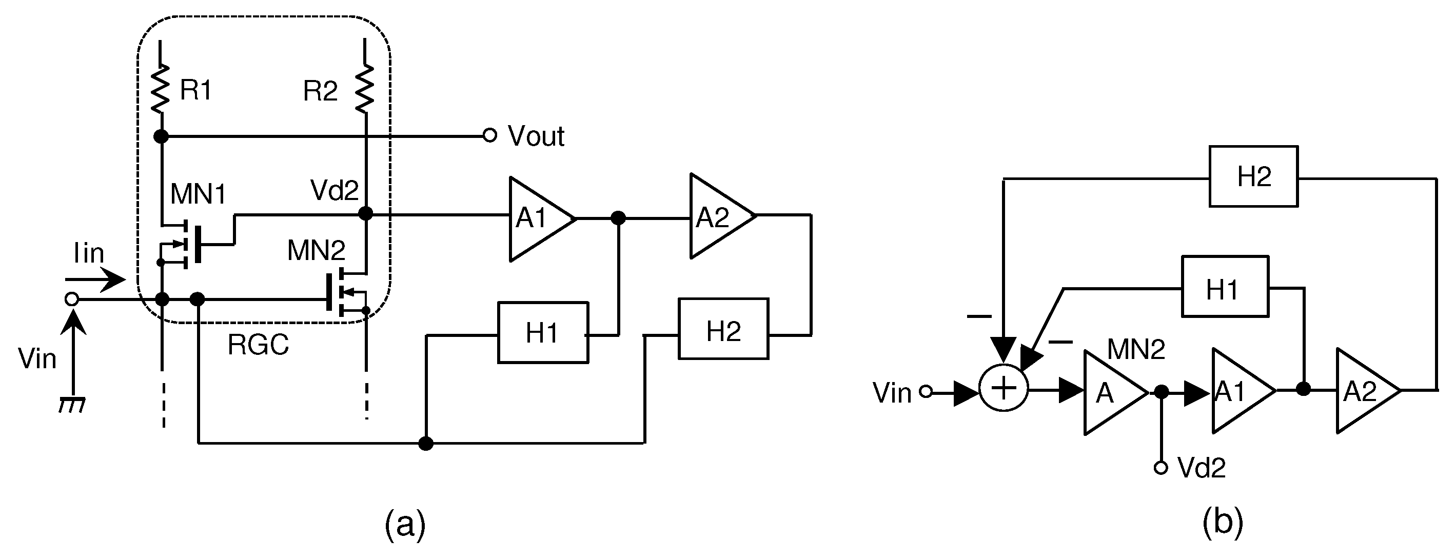
To analyze the transfer function of feedback circuit, we consider the conventional and proposed TIA transfer models as shown in Figure 4 and Figure 5, where A is the gain of common source amplifier (transistor MN or MN), – are the gains of the amplifier in the first and second feedback stage, and – are the gains of the feedback circuit.
From the transfer models shown in Figure 4b and Figure 5b, the conventional and proposed transfer functions of the feedback circuit are expressed as follows:
By comparing Equations (1) and (2), the difference in gain between the conventional and proposed TIAs can be expressed as the following equation:
where, assume that , , , and . Therefore, because the input impedance of the RGC stage can be reduced by the value shown in the aforementioned equations, the frequency of the proposed TIA can be extended compared with the conventional TIA circuit.
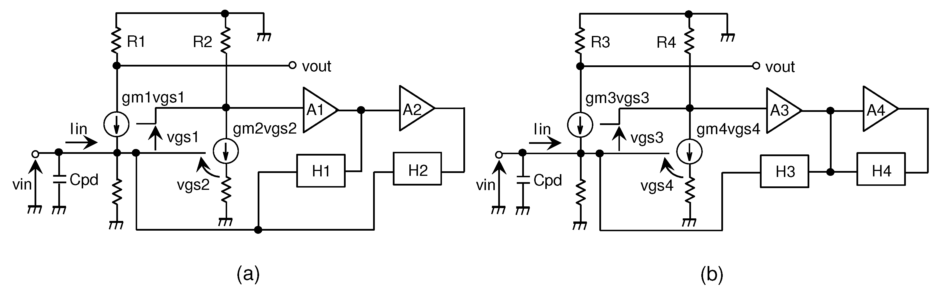
Figure 6 shows the small-signal equivalent circuit for transimpedance gain and cutoff frequency calculation. From this small-signal analysis, the transimpedance gain and cutoff frequency of each TIA are expressed as follows:
where – are the transconductances of MOS transistors MN–MN, respectively, is the equivalent capacitance of the photodiode, – are the feedback resistances in the feedback circuits –, respectively.
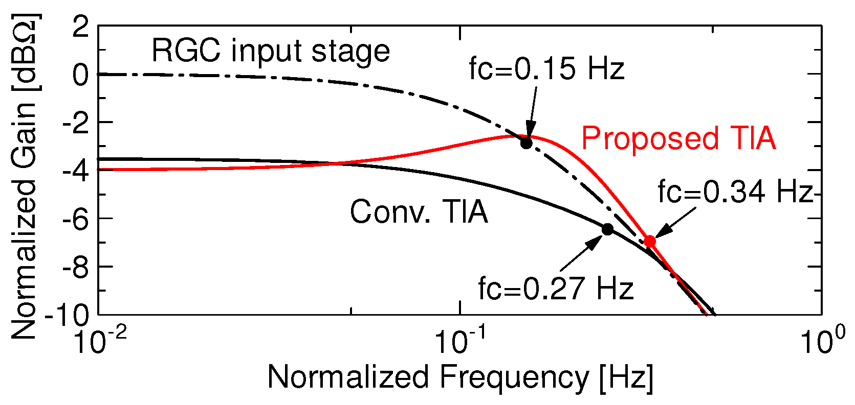
Figure 7 depicts the normalized frequency response, assuming that , , and . The figure shows that the cutoff frequency of the proposed TIA can be expanded compared with that of the conventional TIA.
3. Post-Layout Simulation Results
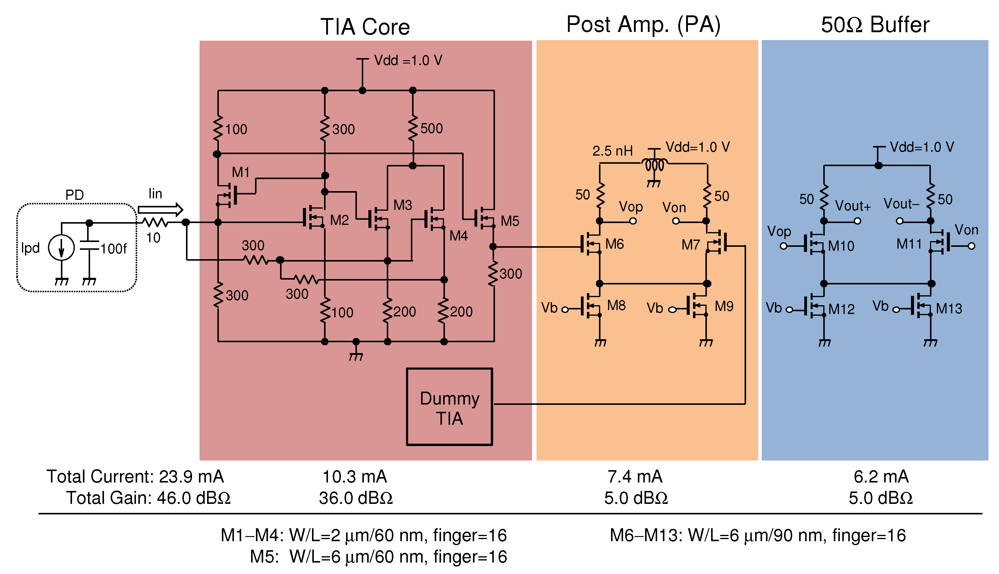
Figure 8 shows the full design of the TIA circuit, as well as the chip layout of the system implemented in a TSMC 65 nm general purpose CMOS process. The first block is the proposed TIA with a local feedback circuit, after which is a post amplifier (PA), required to convert a single-ended input to differential signals. To apply inductive peaking technique for bandwidth enhancement, a center-tapped spiral inductor was used at the drains of the PA stage. Finally, a high-speed unity gain open-drain output buffer was implemented to minimize the impact of directly driving 50 loads at the differential output of the amplifier.
In the first stage, TIA core is designed to wide frequency range and the 100 fF input parasitic capacitance caused by photodiode has been considered. To aim maximum output amplitude when the input DC bias voltage is 0.4 V, the aspect ratio of transistors M and M is set as W/L = 2 m/65 nm, finger = 16. Transistors M and M which is worked as a common drain amplifier correspond to the amplifier stages and shown in Figure 5, respectively. The transistor M is also a common drain amplifer. The aspect ratio of transistors M–M is the same as M and M. As will be described later in this section, the increasing of the input referred noise depends on the value of feedback resistor. Therefore, careful resistor values (300 ) were applied with due consideration of the noise environment. The dummy TIA that has the same circuit as the TIA core, provides a path signal to the PA, and balances the DC voltages at both the inputs of the PA stage.
In the second stage, PA is design as an inductively-peaked differential pair. The shunt inductive peaking is derived from the inductors placed in series with the drain resistors. The output swing is chosen to be 200 mV. For the PA stage designing, an optimal inductance of 2.5 nH was used as trade-off between the bandwidth enhancement in the frequency response and chip area. The center tapped inductor was also chosen from the point of view of chip area. Final stage is the differential output amplifier to drive the 50 load. The MOS transistors M–M is designed as W/L = 6 m/90 nm, finger = 16, to be able to drive the output stage.
The transimpedance gain and the current dissipation of each stage are summarized in Figure 8. Summing the gain contribution of each optical receiver; TIA, PA, and 50 buffer, an transimpedance gain is 46 dB, and power dissipation is 23.9 mW (=23.9 mA × 1.0 V).
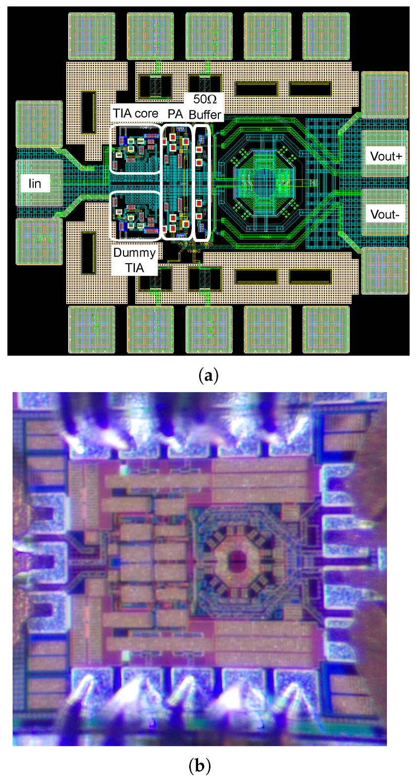
A TIA as shown in Figure 9 was implemented to evaluate its performance. The occupied layout area with I/O and DC pads was 670 m × 580 m, and the total active area of the proposed TIA was 366 m × 225 m.
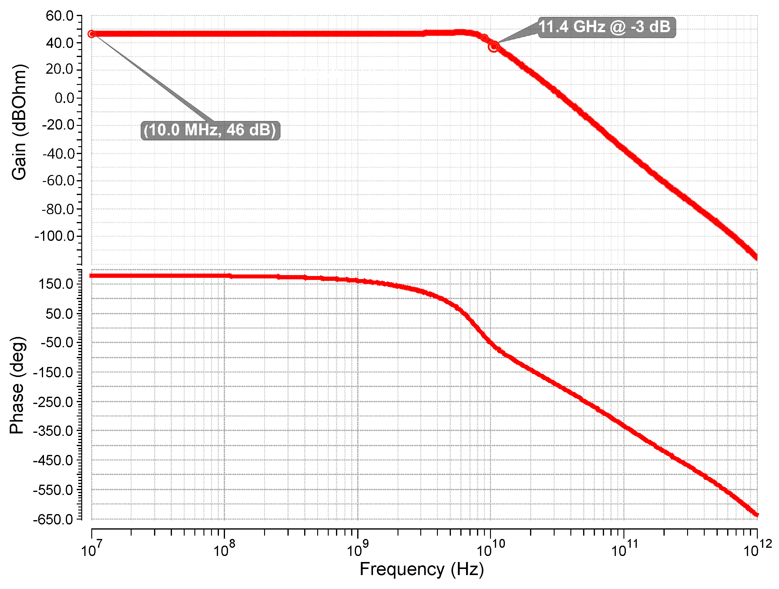
Figure 10 shows the post-layout frequency response of the proposed TIA. The simulation results indicated the differential transimpedance gain was about 46 dB and the −3 dB bandwidth was greater than 11.4 GHz while consuming 23.9 mW of DC power. The measured results are described in Appendix A. To confirm the 2-port S-parameters, a simple function test was carried out using vector network analyzer. The resulting power dissipation was about 26 mW.
From the aforementioned results, Table 1 summarizes the comparison of the current dissipation and cutoff frequency. Hence, the proposed TIA has a high frequency characteristic while suppressing increases in current dissipation.
Figure 11 indicates the equivalent input noise current spectral density. From this figure, we find that the average value is 46.6 on – Hz. Based on the noise equivalent model in [11], the simplified noise equivalent circuit of the proposed TIA is shown in Figure 12, where . From this analysis model, the equivalent noise current spectral density is approximately given by
As shown in the aforementioned equation, we find that the input referred noise increases by adding the feedback section. Hence, we summarize that the value setting of the feedback resistor is relatively more important for this TIA design. The noise increasing is also suggested in post-layout simulation results as shown in Figure 11.
Table 2 compares the performance of the proposed TIA with those of recently published TIAs. The proposed method is superior in term of power dissipation compared with other TIAs implemented using the same 65 nm CMOS technology.
4. Conclusions
To enhance the frequency band of the transimpedance amplifier, we present a local feedback technique in this paper. The numerical analysis showed that the cutoff frequency of the proposed TIA is about 1.3 times wider compared with that of the conventional overall feedback TIA. The post-layout simulation results of the proposed wide-band TIA with a local feedback technique exhibits the following: a −3 dB frequency of 11.4 GHz and a transimpedance gain of 46 dB. The TIA also has a lower power dissipation of 23.9 mW. Thus, the post-layout simulation results indicate that the local feedback technique is useful for optical TIA applications.
Author Contributions
Y.T. contributed to the design of the proposed circuit; Y.T. performed the simulations, the layout design (including TIA top cell level DRC/LVS verification), and the writing—original draft. A.T. provided the designed RF pads, ESD protection circuit, and power bus line for layout design. A.T., T.I. and D.I. performed the chip level DRC/LVS verification. K.K. and M.N. contributed as a supervisor and administrator of this research group. All authors participated in data analysis and paper revision. All authors have read and agreed to the published version of the manuscript.
Funding
This work was supported by a research fund for “Beyond 5G Research and Development Promotion Project” sponsored by the National Institute of Information and Communications Technology (NICT).
Conflicts of Interest
The authors declare no conflict of interest.
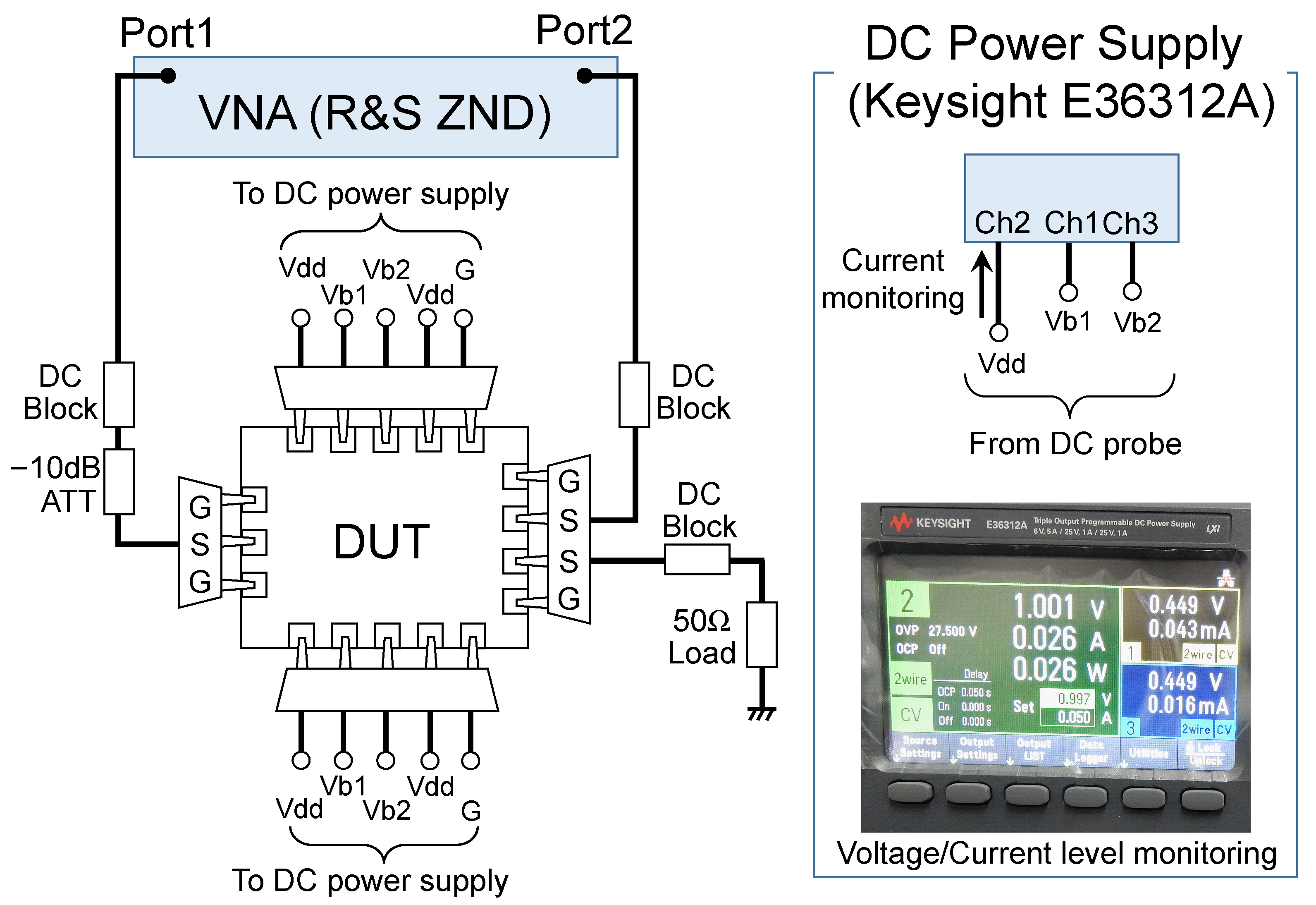
Appendix A. Measurement Results
The performance of the fabricated proposed TIA (Figure 9) was verified with the experimental system illustrated in Figure A1. In order to simplify testings, 2-port S-parameters (i.e., single-ended input/output) was measured using a vector network analyzer (Rohde & Schwarz ZND) with the input power dBm. The results of S and S, presented in Figure A2 show a good agreement between back-annotated (BA) simulation and measurement. On the other hand, the measured S is significantly different from the simulation, at low frequencies. We think the difference between these results is caused by parasitic inductance in the chip, but we still can not identify a precise cause of the difference. The transimpedance gain of single-end TIA was then extracted from S-parameters, and was about 33 dB. When the bias voltage was 450 mV, the measured dissipation of the TIA was 26 mW; hence, this result indicates that the proposed TIA has a low-power characteristic. In these simplify testings, we confirmed only 2-port S-parameters. The 4-port S-parameters will be measured in near future.
Figure A1.
Test setup for S-parameter measurement.

Figure A2.
Comparison of simulated and measured single-ended input/output S-parameters.

References
- Arafin, S.; Simsek, A.; Kim, S.K.; Dwivedi, S.; Liang, W.; Eliyahu, D.; Coldren, L. Towards chip-scale optical frequency synthesis based on optical heterodyne phase-locked loop. Opt. Express 2017, 25, 681–695. [Google Scholar] [CrossRef]
- Costanzo, R.; Bowers, S.M. A current reuse regulated cascode CMOS transimpedance amplifier with 11-GHz bandwidth. IEEE Microw. Wirel. Compon. Lett. 2018, 28, 816–818. [Google Scholar] [CrossRef]
- Costanzo, R.; Bowers, S.M. A 10-GHz bandwidth transimpedance amplifier with input DC photocurrent compensation loop. IEEE Microw. Wirel. Compon. Lett. 2020, 30, 673–676. [Google Scholar] [CrossRef]
- Chen, X.; Takahashi, Y. Floating active inductor based trans-impedance amplifier in 0.18 μm CMOS technology for optical applications. Electronics 2019, 8, 1547. [Google Scholar] [CrossRef] [Green Version]
- Inoue, T.; Tsuchiya, A.; Kishine, K.; Takahashi, Y.; Ito, D.; Nakamura, M. A burst-mode TIA with adaptive response and stable operation for in-vehicle optical networks. In Proceedings of the IEEE International Conference on Electronics Circuits and Systems 2021, Dubai, United Arab Emirates, 28 November–1 December 2021. [Google Scholar] [CrossRef]
- Takemoto, T.; Yamashita, T.; Yazaki, T.; Chujo, N.; Lee, Y.; Matsuoka, Y. A 25-to-28 Gb/s high-sensitivity (−9.7 dBm) 65 nm CMOS optical receiver for board-to-board interconnects. IEEE J. Solid-State Circuits 2014, 49, 2259–2276. [Google Scholar] [CrossRef]
- Kojima, T.; Kunieda, M.; Nakamura, M.; Ito, D.; Kishine, K. Burst-mode CMOS transimpedance amplifier based on a regulated-cascode circuit with gain-mode switching. IEICE Trans. Fundam. 2018, E102-A, 845–848. [Google Scholar] [CrossRef]
- Fukuta, K.; Takahashi, Y.; Ito, D.; Nakamura, M.; Jyo, T.; Nagatani, M.; Nosaka, H. 49.4-dBΩ 46.8-GHz multiple shunt-shunt feedback regulated cascode TIA in 0.25-μm InP-HBT process. In Proceedings of the IEEE Asia Pacific Microwave Conference 2020, Hong Kong, China, 8–11 December 2020. [Google Scholar] [CrossRef]
- Ashtiani, F.; Aflatouni, S.Z. Integrated electro-optical phase-locked loop for high resolution optical synthesis. Optics Express 2017, 25, 16171–16181. [Google Scholar] [CrossRef] [PubMed]
- Lu, Z.; Yeo, K.S.; Ma, J.G. Broad-band design techniques for transimpedance amplifiers. IEEE Trans. Circuit-Syst.-Regul. Pap. 2007, 54, 590–600. [Google Scholar] [CrossRef]
- Park, S.M.; Yoo, H.-J. 1.25-Gb/s Regulated Cascode CMOS transimpedance amplifier for gigabit ethernet applications. IEEE J. Solid-State Circuits 2004, 39, 112–121. [Google Scholar] [CrossRef] [Green Version]
- Jeong, G.-S.; Chi, H.; Kim, K.; Jeong, D.-K. A 20-Gb/s 1.27pJ/b low-power optical receiver front-end in 65nm CMOS. In Proceedings of the IEEE International Symposium on Circuits and Systems (ISCAS) 2014, Melbourne, Australia, 1–5 June 2014. [Google Scholar] [CrossRef]
- Ahmad, W.; Abdulaziz, M.; Törmänen, M.; Sjöland, H. CMOS adaptive TIA with embedded single-ended to differential conversion for analog optical links. In Proceedings of the IEEE ISCAS 2015, Lisbon, Portugal, 24–27 May 2015. [Google Scholar] [CrossRef]
- González, J.L.; Polster, R.; Waltener, G.; Thonnart, Y.; Cassan, E. 10 Gbps, 560 fJ/b TIA and modulator driver for optical networks-on-chip in CMOS 65nm. In Proceedings of the IEEE International New Circuits and Systems Conference 2016, Vancouver, BC, Canada, 26–29 June 2016. [Google Scholar] [CrossRef]
- Hida, A.; Nakane, Y.; Mizuno, S.; Nakamura, M.; Ito, D.; Nakano, S.; Nosaka, H. A wideband current-reuse-RGC TIA circuit with low-power consumption. IEICE Elex. 2019, 16, 20190615. [Google Scholar] [CrossRef] [Green Version]
Figure 1.
Block diagram of a optical heterodyne receiver (modified in [9]).
Figure 1.
Block diagram of a optical heterodyne receiver (modified in [9]).

Figure 2.
Schematic of a conventional TIA.

Figure 3.
Proposed TIA with local feedback.

Figure 4.
Conventional TIA block diagram. (a) A part of RGC and multi-feedback stage. (b) Block diagram for transfer function analysis.
Figure 4.
Conventional TIA block diagram. (a) A part of RGC and multi-feedback stage. (b) Block diagram for transfer function analysis.

Figure 5.
Proposed TIA block diagram. (a) A part of RGC and multi-feedback stage. (b) Block diagram for transfer function analysis.
Figure 5.
Proposed TIA block diagram. (a) A part of RGC and multi-feedback stage. (b) Block diagram for transfer function analysis.

Figure 6.
Small-signal equivalent circuit: (a) conventional multi-feedback stage RGC TIA, (b) proposed RGC TIA.
Figure 6.
Small-signal equivalent circuit: (a) conventional multi-feedback stage RGC TIA, (b) proposed RGC TIA.

Figure 7.
Compared normalized frequency and gain response.

Figure 8.
Full schematic of the proposed TIA, including post amplifier (PA) and 50 buffer.

Figure 9.
Layout and chip microphotograph of the proposed TIA (Top cell with pad). (a) Layout. (b) Microphotograph.
Figure 9.
Layout and chip microphotograph of the proposed TIA (Top cell with pad). (a) Layout. (b) Microphotograph.

Figure 10.
Post-layout simulated frequency response of the proposed TIA.

Figure 11.
Equivalent input noise current spectral density of the proposed TIA.

Figure 12.
Simplified noise equivalent circuit of the proposed TIA: (a) proposed TIA circuit, (b) its equivalent noise model.
Figure 12.
Simplified noise equivalent circuit of the proposed TIA: (a) proposed TIA circuit, (b) its equivalent noise model.


Table 1.
Cutoff frequency and current dissipation comparison of TIA.
| Current Dissipation | Cutoff Frequency | FoM (GHz/mA) | |
|---|---|---|---|
| in TIA Core (mA) | with PA and 50 Buffer (GHz) | ||
| RGC TIA | 8.6 | 6.1 | 0.71 |
| Conventional TIA | 10.1 | 10.3 | 1.09 |
| Proposed TIA | 10.3 | 11.4 | 1.11 |
Table 2.
Performance summary and comparison with other TIA works.
| Reference | [12] (2014) | [13] (2015) | [14] (2016) |
|---|---|---|---|
| CMOS Technology | 65 nm | 65 nm | 65 nm |
| Topology | Inverter | Inverter | Inverter |
| Supply Voltage | 1.0 V | 1.2 V | 2.4 V |
| Transimpedance Gain (dB) | 78 | 51–73 | 51 |
| Bandwidth (GHz) | 11 | 0.55 | 8–12 |
| (fF) | 380 | 1400 | 70 |
| Power Dissipation (mW) | 45.3 | (4.8) * | (0.26) * |
| Input-Referred Noise () | (3.9 | 3.4 | – |
| Chip Area (mm) | 0.75 | (0.006) ** | – |
| Results | Measured | Post-layout | Measured |
| Reference | [2](2018) | [15](2019) | This Work(2022) |
| CMOS Technology | 65 nm | 65 nm | 65 nm |
| Topology | Current reuse | Current reuse | multistage feedback |
| RGC | RGC | RGC | |
| Supply Voltage | 1.0 V | 1.0 V | 1.0 V |
| Transimpedance Gain (dB) | 65.8 | 43 | 46 |
| Bandwidth (GHz) | 11.0 | 10.3 | 11.4 |
| (fF) | 200 | – | 100 |
| Power Dissipation (mW) | 66 | (4.3) * | 23.9 |
| (Measured: 26) *** | |||
| Input-Referred Noise () | 30 | – | 46.6 |
| Chip Area (mm) | 0.25 | – | 0.39 |
| Results | Measured | SPICE | Post-layout |
* Buffer power exempted, ** Active area only, *** See, Appendix A.
Publisher’s Note: MDPI stays neutral with regard to jurisdictional claims in published maps and institutional affiliations. |
© 2022 by the authors. Licensee MDPI, Basel, Switzerland. This article is an open access article distributed under the terms and conditions of the Creative Commons Attribution (CC BY) license (https://creativecommons.org/licenses/by/4.0/).
Share and Cite
MDPI and ACS Style
Takahashi, Y.; Ito, D.; Nakamura, M.; Tsuchiya, A.; Inoue, T.; Kishine, K. Low-Power Regulated Cascode CMOS Transimpedance Amplifier with Local Feedback Circuit. Electronics 2022, 11, 854. https://doi.org/10.3390/electronics11060854
AMA Style
Takahashi Y, Ito D, Nakamura M, Tsuchiya A, Inoue T, Kishine K. Low-Power Regulated Cascode CMOS Transimpedance Amplifier with Local Feedback Circuit. Electronics. 2022; 11(6):854. https://doi.org/10.3390/electronics11060854
Chicago/Turabian StyleTakahashi, Yasuhiro, Daisuke Ito, Makoto Nakamura, Akira Tsuchiya, Toshiyuki Inoue, and Keiji Kishine. 2022. "Low-Power Regulated Cascode CMOS Transimpedance Amplifier with Local Feedback Circuit" Electronics 11, no. 6: 854. https://doi.org/10.3390/electronics11060854
Note that from the first issue of 2016, this journal uses article numbers instead of page numbers. See further details here.