Article

Demystifying Non-Isolated DC–DC Topologies on Partial Power Processing Architectures

1
Electronics and Computing Department, Mondragon Unibertsitatea, 20120 Hernani, Spain
2
Electronics Engineering and Communication Department, Universidad Zaragoza, 50018 Zaragoza, Spain
*
Author to whom correspondence should be addressed.
Electronics 2022, 11(3), 480; https://doi.org/10.3390/electronics11030480
Submission received: 10 December 2021 / Revised: 26 January 2022 / Accepted: 3 February 2022 / Published: 6 February 2022

Abstract

:
This paper discusses the possibility of achieving partial power processing with non-isolated DC–DC topologies. To this end, partial power converter architectures are seen as an interesting solution for reducing the power processed by the converter. We observed via simulations that single-inductor non-isolated topologies cannot achieve partial power processing since the obtained current and voltage waveforms were the same as those found in a full-power converter. However, when using double inductor non-isolated topologies, reduced current and improved efficiencies were achieved. In order to confirm the results obtained from the simulations, single- and double-inductor topologies were tested experimentally. Finally, it was concluded that a double-inductor non-isolated topology can improve its performance by using partial power processing.

1. Introduction

The increasing global energy demand over the last 20 years means that electric energy is gaining more and more importance in our daily lives [1,2,3]. Furthermore, when taking into account the imminent emergence of the electric vehicle (EV) [4,5,
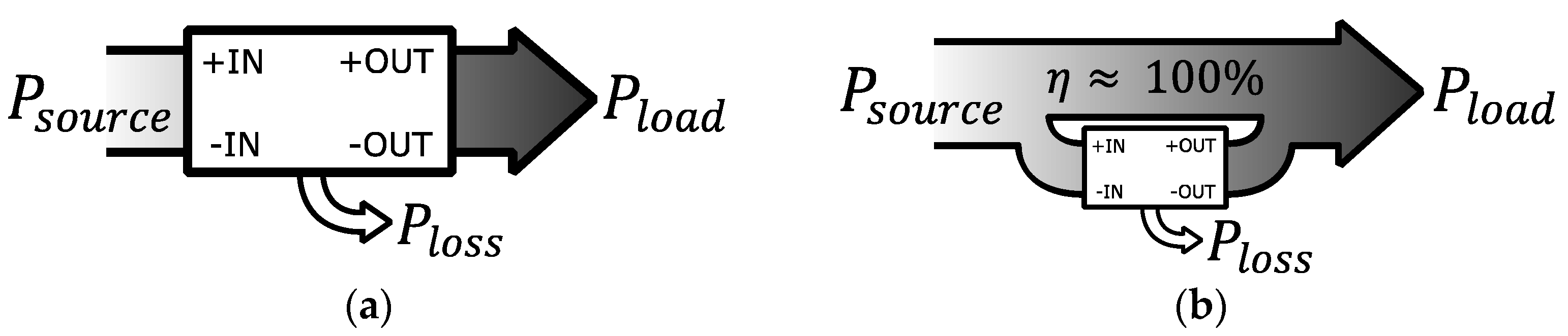
6], there is no doubt that the electric energy sector will be of great importance in the immediate future. Inside the electric energy sector, the power converter is a key device whose design and behavior directly affect its efficiency, its cost, and the size of the final solution. Therefore, over the last decade, with the aim of improving converter performance, partial power processing (PPP)-based strategies have been presented as promising solutions regarding power converter downsizing and system efficiency improvements. PPP strategies aim to reduce the amount of power that needs to be processed by the power converter. To explain this, 
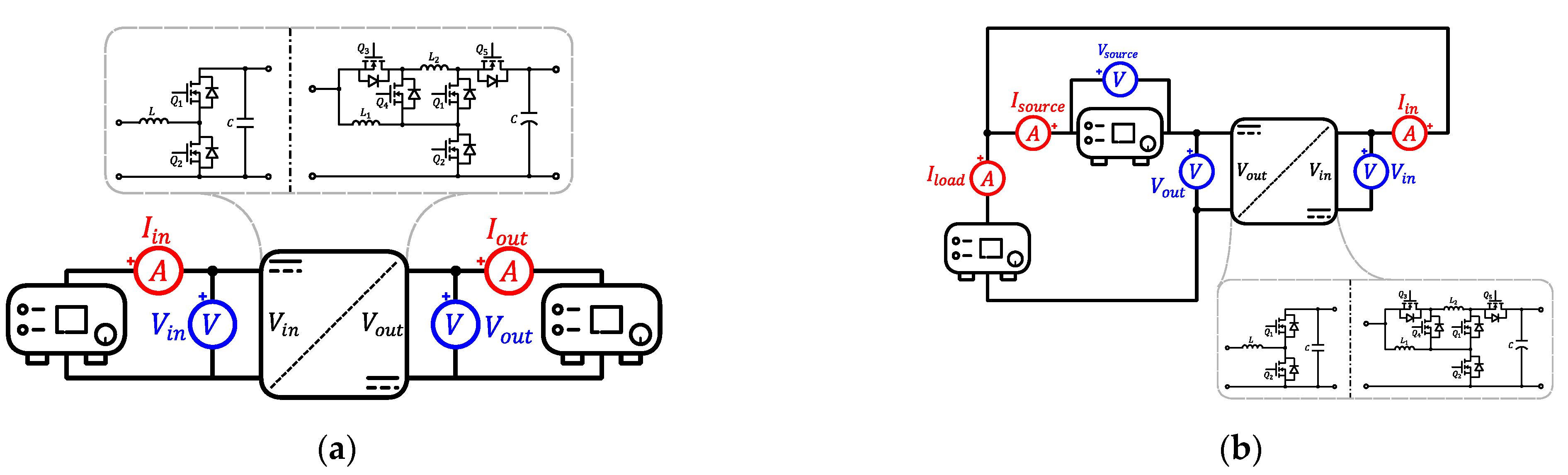
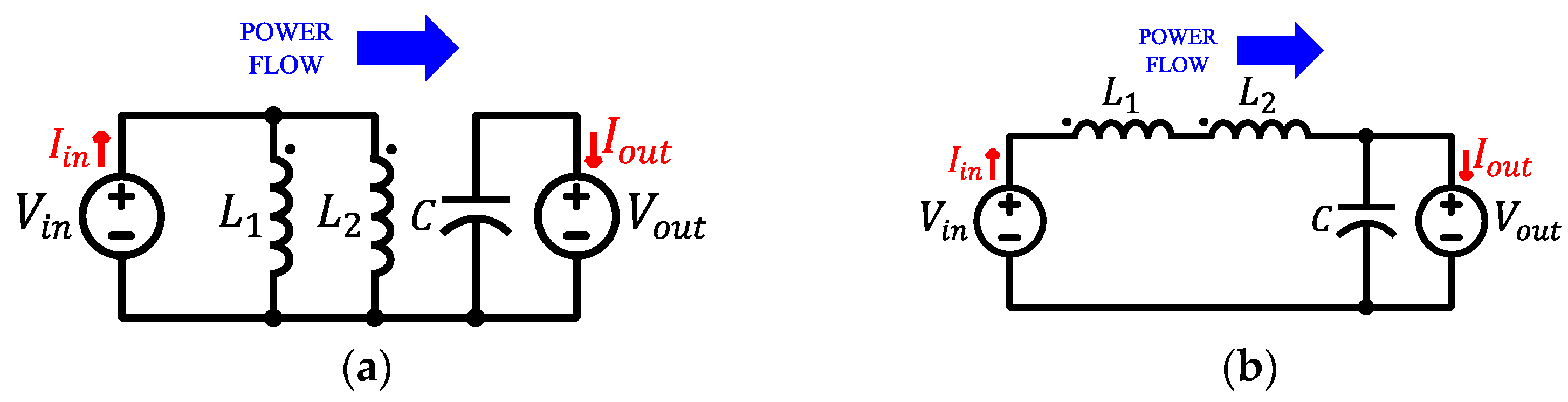
Figure 1 presents a power flow comparison between a full power processing (FPP) solution and a PPP solution. As can be observed, an FPP converter (Figure 1a) processes 100% of the source power, generating a given quantity of losses. However, a PPP (Figure 1b) converter only processes a fraction of the power that flows from the source to the load. This allows for a reduction in the size and power losses of the converter. According to the literature, three different types of PPP strategies exist for DC–DC applications [7]: differential power converters (DPCs), partial power converters (PPCs), and mixed strategies. On the one hand, DPCs are aimed at correcting current imbalances that exist between different elements connected in series to a common voltage bus [8,9]. On the other hand, PPCs’ main goal is to control the power flow between a source and a load with different voltage or current levels [10,11]. Finally, the mixed strategies group contains different solutions that can offer better performance than DPCs and PPCs under specific conditions.
Focusing on PPCs, there exist two main groups: the architectures that, in order to avoid a short-circuit, require isolated topologies and the ones that do not. Regarding the first group, many different authors have achieved reduced sizes and more efficient solutions. For example, authors in [12] prove that PPP can be achieved with a PPC architecture if an adequate isolated topology is implemented; for example, a phase shifted full bridge (PSFB). Additionally, [13] concludes that a dual active bridge (DAB) topology implemented on a PPC architecture achieves a reduced electrical stress and efficiency improvement in comparison to its FPP counterpart. However, when it comes to implementing non-isolated topologies on PPC architectures, the authors of [10,14,15] show that using a buck-boost topology on a PPC architecture results in FPP rather than PPP.
Regarding non-isolated DC–DC topologies, the literature presents many different solutions. On the one hand, authors in [16] present and compare non-isolated DC–DC converters for renewable applications. On the other hand, authors from [17] review the main high-gain DC–DC topologies and address their main challenges. Additionally, the authors of [18] present single- and multi-stage DC–DC converters for EV applications.
Bearing this in mind, the present paper aims to extend the analysis of non-isolated topologies implemented on PPC architectures that achieve PPP. To be more precise, it aims to prove that certain DC–DC, non-isolated topologies can improve their performance when implemented on a PPC architecture. Indeed, there exists a lack of analysis around non-isolated topologies on PPC architectures. The authors of [19] conclude that a double-inductor topology can achieve PPP, but they do not demonstrate it experimentally. Thus, Section 2 starts by describing the PPC architecture that will be implemented for this analysis. Then, Section 3 and Section 4 simulate and compare two different non-isolated topologies implemented on a PPC architecture. Next, Section 5 confirms the results experimentally obtained through the simulations. Finally, Section 6 discusses how PPP was achieved with one of the topologies presented previously and Section 7 presents our conclusions.

2. PPC Architecture Description

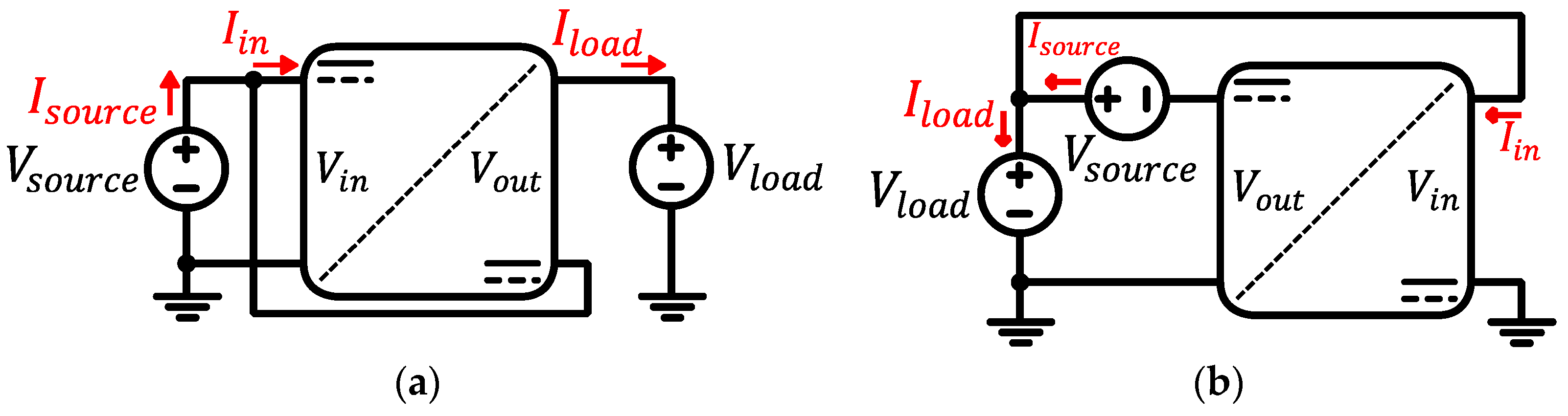
Inside PPC architectures, there exist two main groups: the ones that, in order to avoid a short circuit, require isolated topologies (Figure 2a) and the ones that do not (Figure 2b). Architectures that require isolated topologies are known as input-parallel-output-series (IPOS) and if a non-isolated topology is implemented in one there exists the risk of short-circuiting V s o u r c e . Regarding the architectures that permit non-isolated topologies, the authors of [20] present them as fractional converters (FC). Figure 2b presents an FC-type PPC for a voltage step-up application.
As can be observed, there exists no risk of short-circuiting any of the sources if a non-isolated topology is implemented. On the other hand, the processed power ratio of the converter ( K p r ) achieved by the FC is defined as Equation (1). It can be seen that it consists of the division between the power processed by the converter ( P i n ) and the source power ( P s o u r c e ) . Analyzing Equation (1), it can be concluded that the FC is limited to a working operation range where 1 G V 2 . Indeed, if this condition is fulfilled, the obtained K p r is lower than 1, which means that the power processed by the converter is lower than that supplied by the source. However, when G V exceeds a value of 2, the resulting K p r is higher than 1. This means that the power converter is out of the PPP region and all the benefits are lost.
K p r F C = P i n P s o u r c e = V i n · I i n V s o u r c e · I s o u r c e = G V 1
where P i n ,   V i n , and I i n are the input power, voltage, and current of the converter, respectively, P s o u r c e , V s o u r c e , and I s o u r c e are the source power, voltage, and current, respectively, and G V is the static voltage gain of the application ( V l o a d / V s o u r c e ) .
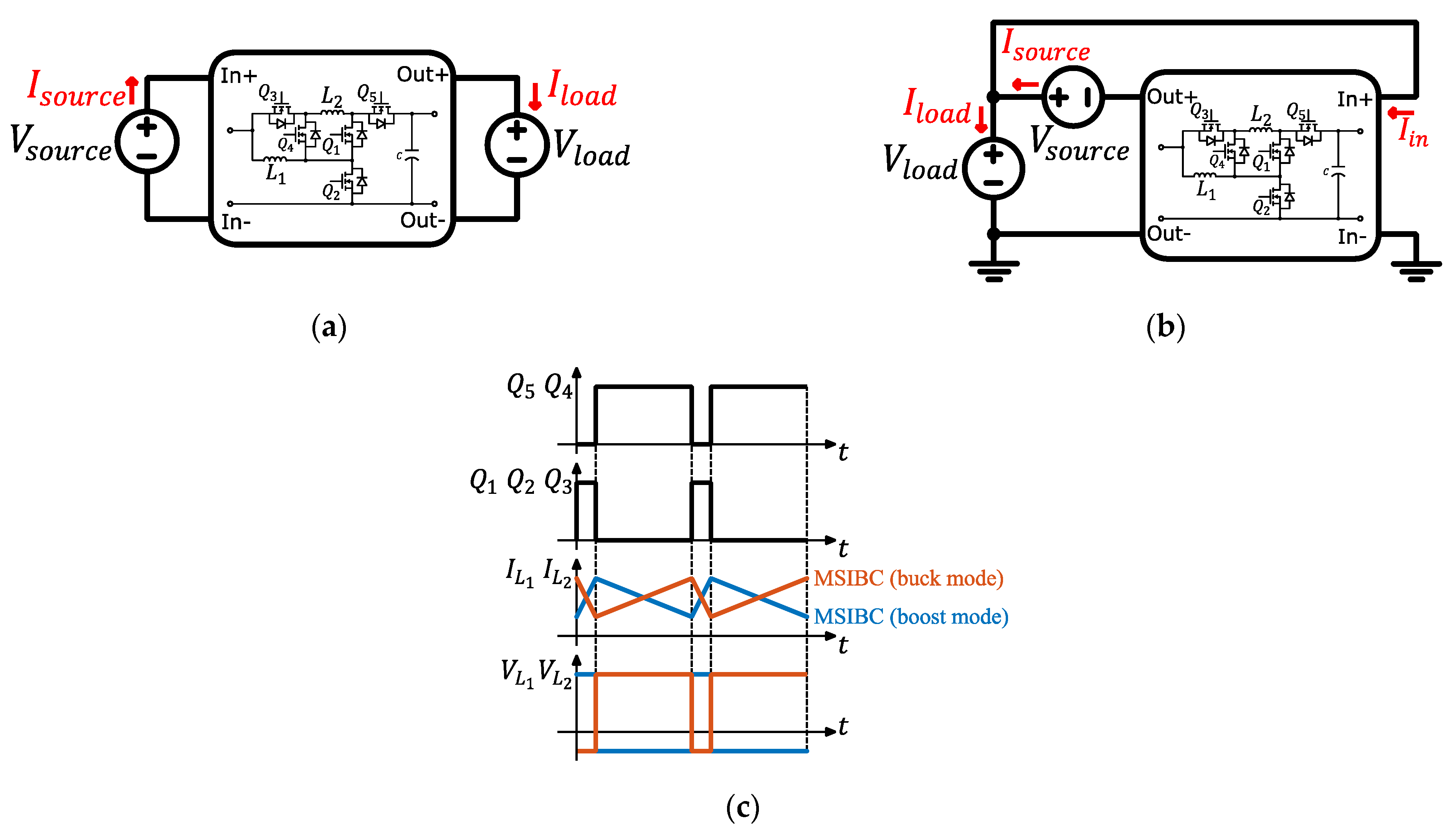
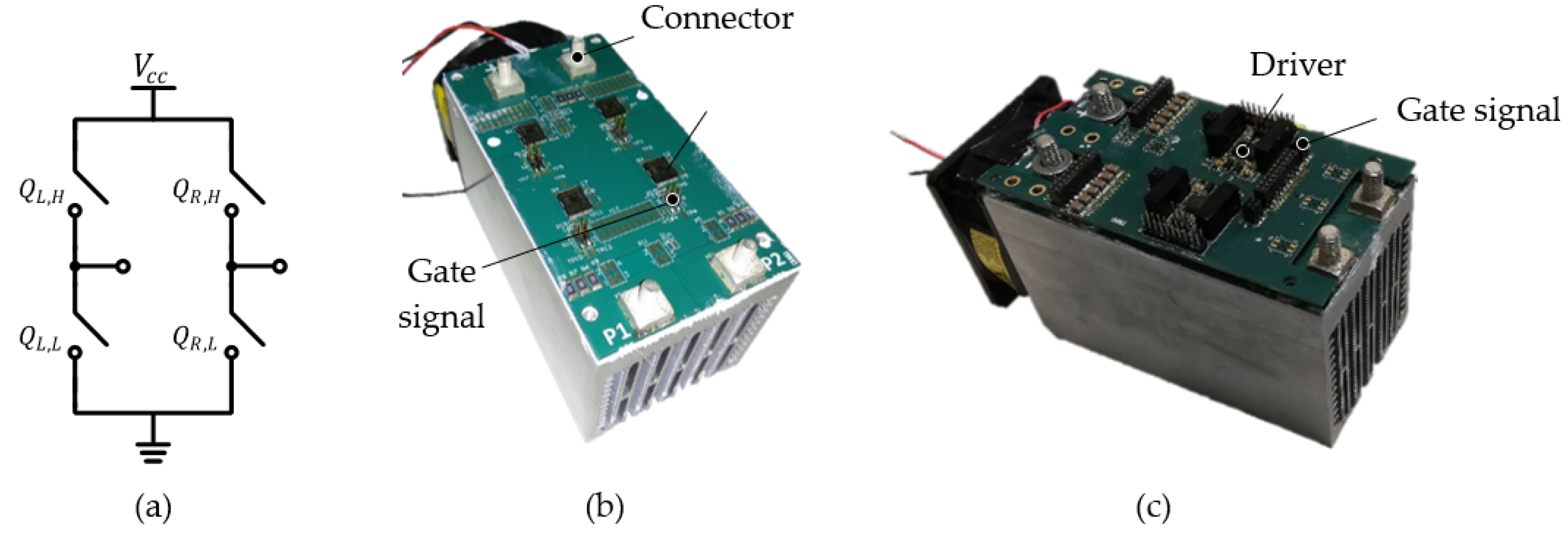
As mentioned before, this paper aims to analyze the behavior of non-isolated topologies when they are implemented on a PPC architecture— on an FC, to be more precise. To this end, two different case studies are proposed: a single-inductor topology and a double-inductor topology. The reason for selecting these two topologies is their simplicity. The single inductor consists of a well-known topology, the half-bridge (HB). On the other hand, the double-inductor topology is the modified switched inductor boost converter (MSIBC). This topology works in a similar way to the HB, but it is capable of parallelizing or serializing the inductors. Other multi-stage or resonant non-isolated topologies are not considered due to their complexity and number of components.

3. Single Inductor Topology Case Study

The present section will focus on the analysis of a conventional single-inductor topology: a HB. With the aim of observing the benefits that the FC architecture may present, 
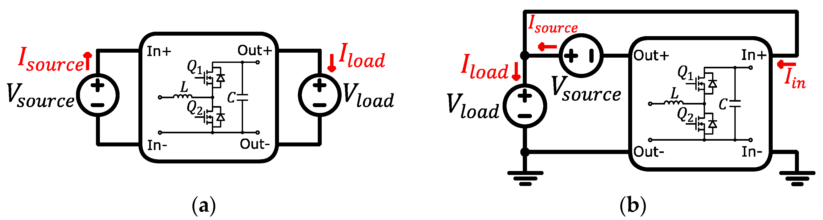
Figure 3a,b show a comparison of two circuits: a full power converter (FPC)-HB and a PPC-HB, respectively.
Table 1 presents the main electrical parameters that define the simulation conditions. As can be observed, the defined source and load voltage levels result in a G V value of 1.25, which meets the 1 G V 2 working condition.
The values defined in Table 1 and Table 2 describe the design parameters of each of the solutions presented in Figure 3. Comparing the results from both solutions, the first difference that exists between them is the input/output voltage levels. In the case of the FPC-HB, they correspond to the source and load values. However, the input voltage of the PPC-HB is proportional to the load and the output consists of the difference between the source and the load. Regarding the K p r , it is expected to be a quarter in the PPC case, achieving a maximum processed power of 375 W in the converter. Moreover, the power flow inside each solution provokes two different working conditions. On the one hand, the FPC-HB will work as a boost, whereas the PPC-HB will work as a buck. Finally, with the aim of maintaining a fair comparison, the same storage elements and semiconductors are implemented in both cases.
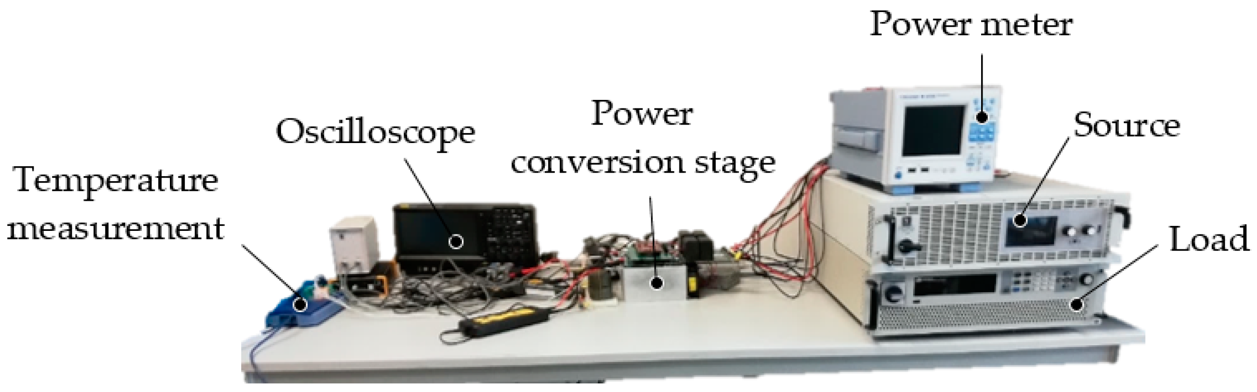
Before analyzing the simulation results, it is important to mention that only semiconductor power losses are considered in the simulated circuits. Indeed, the passive elements are considered ideal and their internal resistances are neglected. Thus, in order to calculate the theoretical switching losses of the semiconductors previously characterized curves have been used.
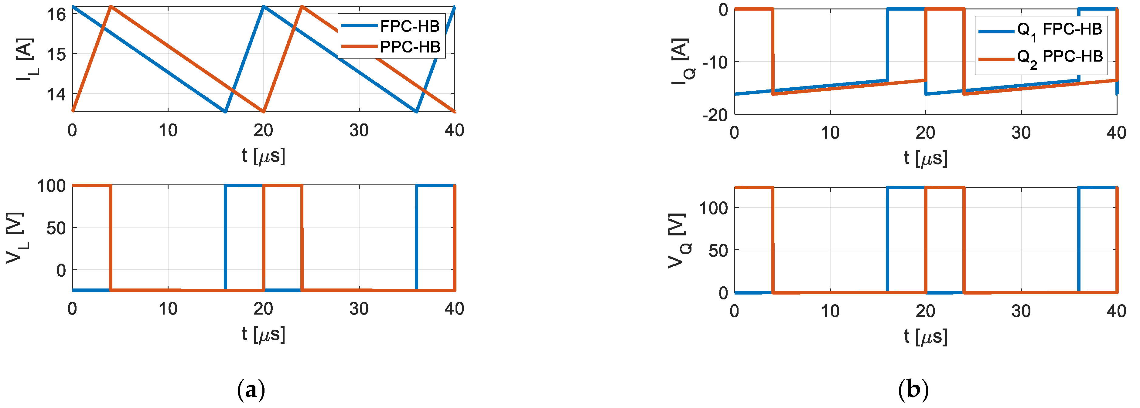
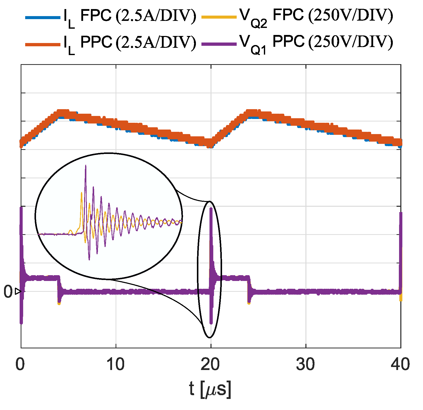
Figure 4a presents inductor voltage and current waveforms in the steady-state. It can be observed that both architectures attain the same inductor voltage and current levels. In addition, the current ripple obtained by each solution is exactly the same. Figure 4b presents the current and voltage waveforms of the semiconductors. Due to the fact that each HB is working in a different mode (boost and buck, respectively), their results are different. The same conclusion is obtained when it comes to the capacitor; the capacitor current and voltage waveforms obtained by both solutions are identical (Figure 4c). In conclusion, it is observed that the PPC-HB does not offer any improvement in terms of current or voltage reduction. Indeed, it results in a conventional HB converter working in buck mode. These results demonstrate in a simple way that implementing a HB topology in an FC-type PPC architecture does not present any benefits.
Finally, Table 3 presents the obtained power losses, efficiencies (system and converter), and K p r results. As can be observed, the converter efficiency obtained by the FPC-HB is higher than that obtained by the PPC-HB. However, when comparing the system efficiency, both achieve the same value. Note that due to the non-ideal circuit, the K p r is not exactly 0.25 as in the ideal circuit. The system and converter efficiencies of a PPC architecture are related to the K p r (Equation (2)). Regarding the power losses, as expected, they are equally distributed across both solutions. In conclusion, both solutions can be defined as identical.
η s y s = 1 K p r · ( 1 η c o n v )
where η s y s and η c o n v represent the efficiency of the system and the converter, respectively.

4. Double Inductor Topology Case Study

Similarly to the previous section, the present one aims to analyze the behavior of a double-inductor non-isolated topology when it is implemented on an FC architecture. For this case, a MSIBC is proposed [21]. This topology is recommended to achieve high voltage by using the principle of parallel charging and series discharging of inductors. Again, the two solutions to compare consist of an FPC-MSIBC and a PPC-MSIBC (Figure 5a,b, respectively). With respect to the simulation conditions, Table 4 presents the main electrical parameters.
The values defined in Table 4 and Table 5 describe the design parameters of each solution in Figure 5. Again, the input/output voltage values and the operation mode of the power converter vary from the FPC-MSIBC to the PPC-MSIBC. When it comes to the passive and active components, compared to the single-inductor topology, the only value changed is that of the inductances, with each being half that of the single inductance.
In the same way as in the previous section, the developed simulations do not consider the switching losses; thus, these are obtained from previously characterized curves.
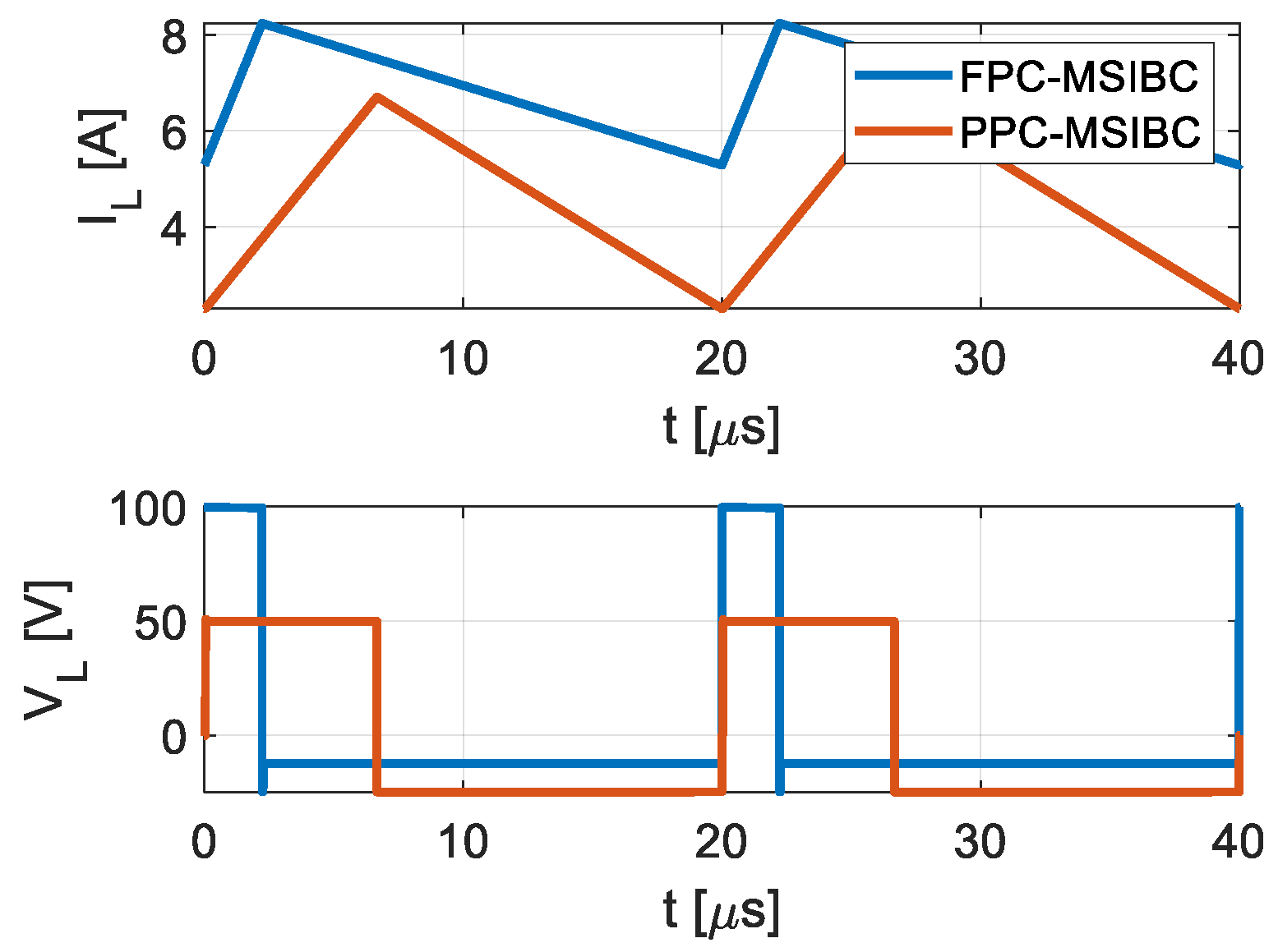
When it comes to the obtained results, 
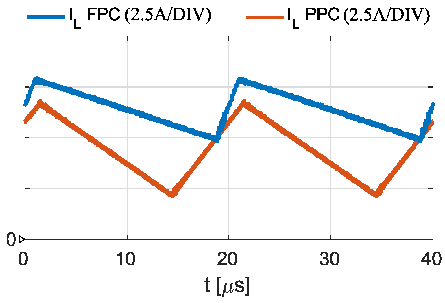
Figure 6 presents inductors’ current and voltage steady-state waveforms. Unlike the single-inductor comparison, the PPC-MSIBC attains a lower inductor RMS current than the FPC-MSIBC; 4.67 A and 6.8 A, respectively. This will directly affect the current that the semiconductors can handle.
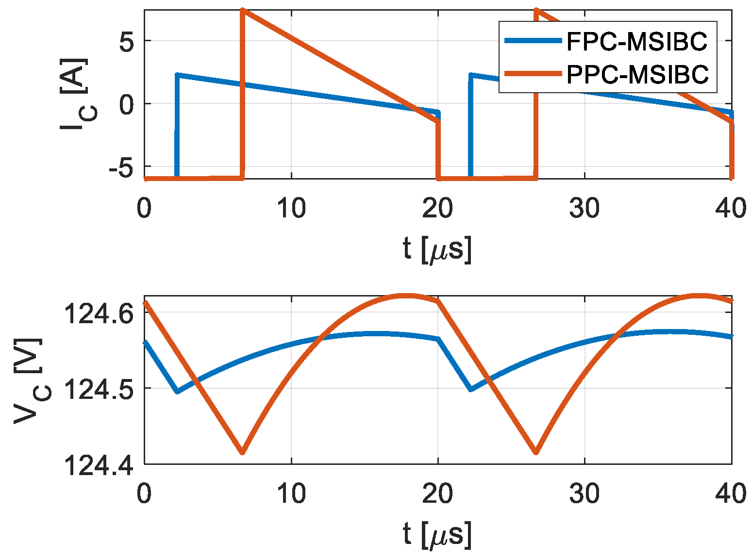
On the other hand, when it comes to the capacitor, Figure 7 shows the voltage and current waveforms obtained by both architectures. In this case, the resulting capacitor RMS current of the MSIBC-PPC is higher than that of the MSIBC-FPC; 4.72 A and 2.27 A, respectively. As a consequence, for the same capacitance value the output voltage ripple is higher at the MSIBC-PPC. In short, for the MSIBC-PPC the current through the inductors is reduced, whereas at the output capacitor it is increased.
Finally, Table 6 shows the power loss, efficiency (system and converter), and K p r results. Similar to the single inductor analysis, the converter efficiency obtained by the FPC-MSIBC is higher than that obtained by the PPC-MSIBC. However, in this case, the PPC-MSIBC achieves a better system efficiency. This means that the total amount of losses produced by the converter has been reduced by using an FC-type PPC architecture.

5. Experimental Results

5.1. Prototype Design

For the design of the prototype, the system specifications presented in Table 2 (for single inductor) and Table 5 (for double inductor) are defined.
Two different designs were mounted in the laboratory: a single 150 µH inductance for the HB (Figure 8a) and two 75 µH inductances for the MSIBC (Figure 8b). For the magnetic cores, a PM8770H and a PM6249 were used, respectively (both cases with CF139 ferrite). Then, the same semiconductor and capacitor components were used for both cases, see Table 7.
Figure 9 shows the constructed full bridge for the experimental tests. As can be observed, it consists of two main layers. The first one, presented in Figure 9b, represents the power layer, which contains only the connectors and semiconductors. The second one (Figure 9c) represents the driver layer, which contains the necessary components to adapt the signals coming from the controller to the gate of the semiconductors. This prototype will be used for testing both topologies: the single-inductor topology and the double-inductor topology. In the case of the HB, a single branch is required. Thus, based on Figure 9a, Q L , H and Q L , L will act as Q 1 and Q 2 in Figure 3, respectively. However, for the MSIBC, two power blocks are needed:
  • Power block 1 uses Q L , H , Q R , H , and Q R , L to act as Q 3 ,   Q 4 , and Q 2 , respectively (Figure 5).
  • Power block 2 uses Q R , H   and Q R , L to act as Q 5 and Q 1 , respectively (Figure 5).

5.2. Description of the Experimental Set-up

Figure 10 shows a simplified electric diagram of the implemented configurations. On the one hand, Figure 10a presents the set-up for measuring the current and voltage values of the FPC architectures. The system and converter current/voltage waveforms coincide and thus only two voltage and two current measures are necessary:
  • V i n and V o u t , which also represent V s o u r c e and V l o a d .
  • I i n and I o u t , which also represent I s o u r c e and I l o a d .
On the other hand, for FC (Figure 10b) six different parameters are required to measure the voltage and current of the converter and the system:
  • V s o u r c e , V o u t , and V i n , where the latter coincides with V l o a d .
  • I l o a d , I i n , and I s o u r c e , where the latter coincides with I o u t .
Additionally, the current through the inductors ( I L ) and the temperature of each semiconductor is measured.
Finally, Figure 11 shows a real image of the set-up used for the experimental tests. More detailed information is given in Appendix A.

5.3. Results

5.3.1. Single Inductor Topology

Figure 12 shows the experimental results obtained for a single-inductor topology. When it comes to the inductor current, it is observed that both solutions present the same current levels. Additionally, similar waveforms are obtained with the FPC and the PPC in terms of semiconductor voltage. Nevertheless, when in detail the overshoot that the semiconductors must withstand in detail, the PPC provokes higher values. It must be mentioned that the great overshoot values are produced due to the non-optimized layout of the power converter.
Table 8 presents the obtained power loss, efficiency, and K p r values. Compared to Table 3, higher conduction losses were observed. This is mainly due to the inherent resistance of the inductor. It can also be observed that the converter efficiency achieved by the PPC is worse than that of the FPC, but, due to its reduced K p r , the system efficiency increases. By comparing both system efficiencies, it is observed that both values are very similar. Indeed, there exists just a negligible difference of 0.2%. In conclusion, a single-inductor topology, such as the HB, does not improve its performance when it is implemented on an FC-type PPC architecture. As a consequence, it cannot be considered a PPP solution.

5.3.2. Double Inductor Topology

Figure 13 presents the inductor current obtained by each solution. As can be observed, the obtained current levels are different. In the case of the FPC, the RMS current is around 6.45 A, whereas for the PPC it is 4.62 A. Additionally, although the PPC presents a higher ripple, its peak value is lower than that obtained by the FPC.
With the aim of observing the thermal behavior of each solution, Figure 14a,b show the temperature evolution of the switches on the FPC and the PPC, respectively. As can be observed, there is a critical semiconductor that heats more easily than the rest of the components in both solutions. In the case of the FPC-MSIBC, the semiconductor that heats the most is Q 1 . In fact, it achieves a maximum temperature of 50.6 °C, whereas the next semiconductor only heats up to 28 °C. On the other hand, when it comes to the PPC-MSIBC, Q 3 is the most critical semiconductor. However, its maximum temperature is around 45.83 °C (5 °C less than the FPC-MSIBC). The other semiconductors barely reach 25 °C.
Lastly, Table 9 shows the power loss, efficiency, and K p r results. As one can see, although the converter efficiency of the PPC-MSIBC is poor, due to the reduced K p r the achieved system efficiency of the PPC-MSIBC is two points higher than that of the FPC-MSIBC. In conclusion, an FC-type PPC architecture can improve the system efficiency and reduce the current stress of the inductors and semiconductors of a MSIBC. In other words, it can achieve PPP.
When it comes to the power losses, Table 9 concludes that the switching losses predominate.—they account for 86% of the total losses. When implementing a MSIBC topology on a PPC architecture, both the conduction losses and the switching losses are reduced by 40%. This reduction in the losses causes an efficiency improvement of around 2.25%.

6. Discussion

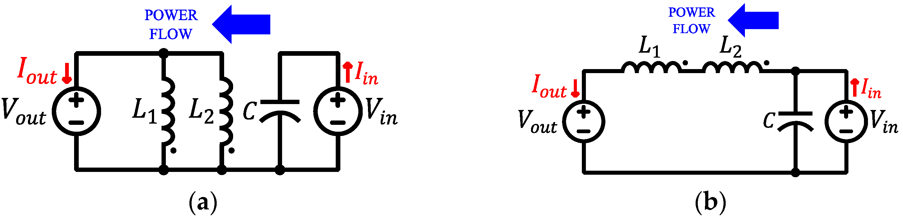
The present section aims to explain the reason we achieved PPP with a MSIBC and not with a HB. With this in mind, it is essential to compare the voltage observed by the inductor when it is implemented on an FPC and a PPC architecture.
In the first place, when it comes to the HB (see Figure 15a), the voltage observed by its inductor can be defined by two switching states (Equation (3)).
V L = { V ( 1 ) V ( 0 ) V ( 1 ) V ( 2 ) }
Since the values of V ( 0 ) , V ( 1 ) , and V ( 2 ) vary depending on the architecture in which the HB is implemented, the next step is to substitute them for their corresponding values. In the case of the FPC-HB, V ( 1 ) = V i n and V ( 2 ) = V o u t (from Table 2), whereas in the case of the PPC-HB, V ( 1 ) = V o u t and V ( 2 ) = V i n (Table 2). Regarding V ( 0 ) , for both solutions it has a value of 0. The results are shown in Equations (4) and (5), where the same absolute voltage values are achieved with an FPC-HB and a PPC-HB. In conclusion, the voltage observed by the inductor does not change whether it is implemented on an FPC or a PPC architecture.
V L F P C , H B = { V ( 1 ) V ( 0 ) = 100 0 = 100 V V ( 1 ) V ( 2 ) = 100 125 = 25 V }
V L P P C , H B = { V ( 1 ) V ( 0 ) = 25 0 = 25 V V ( 1 ) V ( 2 ) = 25 125 = 100 V }
When it comes to the MSIBC (Figure 15b), a different result is obtained. In this case, the inductors’ voltage is defined by Equation (6). It is divided by two at the second switching state due to the series connection of L 1 and L 2 .
V L 1 , 2 = { V ( 1 ) V ( 0 ) V ( 1 ) V ( 2 ) 2 }
The next step is to substitute V ( 0 ) , V ( 1 ) , and V ( 2 ) for their corresponding values. In the case of the FPC-MSIBC, V ( 1 ) = V i n and V ( 2 ) = V o u t (from Table 5), whereas in the case of the PPC-MSIBC, V ( 1 ) = V o u t and V ( 2 ) = V i n (from Table 5). The obtained results are shown in Equations (7) and (8). As can be seen, the voltage observed by the inductors varies depending on whether they are implemented on an FPC or PPC architecture. As a consequence, the duty cycle at which the converter will work is affected (Equations (9) and (10)). More detailed information about the origin of Equations (9) and (10) is given in the appendix.
V L F P C , M S I B C = { V ( 1 ) V ( 0 ) = 100 0 = 100 V V ( 1 ) V ( 2 ) 2 = 100 125 2 = 12.5 V }
V L P P C , M S I B C = { V ( 1 ) V ( 0 ) = 25 0 = 25 V V ( 1 ) V ( 2 ) 2 = 25 125 2 = 50 V }
D F P C , M S I B C = V o u t V i n V o u t + V i n = 125 100 100 + 225 = 0.11
D P P C , M S I B C = 2 · V o u t V o u t + V i n = 2 · 25 25 + 125 = 0.33
Comparing both duty cycles from (9) and (10), it can be observed that the one achieved by the FPC-MSIBC is more extreme (closer to 0), which involves an increase in the RMS current of the inductor and the other semiconductors.

7. Conclusions

With the aim of extending the analysis of power converters that achieve PPP, this paper was focused on studying the applicability of non-isolated topologies on FC-type PPC architectures. Through simulations, it was observed that a conventional single-inductor topology (such as the HB) did not improve the results obtained by its full power version. In fact, the current and voltage waveforms of the components inside the converter were identical on an FPC-HB and a PPC-HB. On the other hand, when a double-inductor topology (such as the MSIBC) was implemented on an FC-type PPC architecture, the current through the inductors was reduced, along with that of the other semiconductors. As a consequence, the power losses were reduced and the efficiency of the system was improved. This was experimentally proven in Section 5. To sum up, this paper proves that a non-isolated double-inductor topology (in this case a MSIBC) can achieve PPP when it is implemented on an FC-type PPC architecture. This way, the current stress of its components and the losses produced by them is reduced.

Author Contributions

Investigation, J.A. and A.A.; resources, A.A.; supervision, I.A., J.S.A.-S. and C.B.; validation, J.A.; writing—original draft, J.A.; writing—review and editing, J.A., I.A., A.A. and J.S.A.-S. All authors have read and agreed to the published version of the manuscript.

Funding

This research received no external funding.

Conflicts of Interest

The authors declare no conflict of interest.

Appendix A

The objective of this appendix is (i) to list the equipment that was used in the experimental tests and (ii) to define the main analytical equations that describe the behavior of the MSIBC.
Table A1 details the equipment used in the experimental tests described in Section 5.
Table A1. Equipment used in the experimental tests.
DescriptionReference
SourceITECH IT6012C-800-40
LoadEA-ELR 9750-22
Power meterYOKOGAWA WT500
Temperature measurementPico TC-08
Additionally, we here present an analysis of the continuous conduction mode (CCM) of the MSIBC. This topology allows for bidirectional power flow and can be represented by two switching states. In state 1 semiconductors Q 1 , Q 2 , and Q 3 are switched on (and Q 4 and Q 5 are switched off), while in state 2 semiconductors Q 4 and Q 5 are switched on (and Q 1 , Q 2 , and Q 3 are switched off). In state 1, both inductors are connected in parallel, whereas in state 2 they are connected in series.
Figure A1 shows the two switching states of a boost mode operation, which is related to the FPC-MSIBC (Figure 5a). Then, by equalizing the voltage observed by the inductors in each period (A1), the duty cycle is obtained (A2).
Figure A1. Boost mode operation. (a) Switching state 1. (b) Switching state 2.
Electronics 11 00480 g0a1
V i n · D F P C , M S I B C = V i n V o u t 2 · ( 1 D F P C , M S I B C )
D F P C , M S I B C = V o u t V i n V o u t + V i n
Figure A2 shows the two switching states of a buck mode operation, which are related to the PPC-MSIBC (Figure 5b). By equalizing the voltage observed by the inductors in each period (A3), the duty cycle is obtained (A4).
Figure A2. Buck mode operation. (a) Switching state 1. (b) Switching state 2.
Electronics 11 00480 g0a2
V o u t · D P P C , M S I B C = V i n V o u t 2 · ( 1 D P P C , M S I B C )
D P P C , M S I B C = 2 · V o u t V o u t + V i n

References

  1. Data and Statistics—IEA. Available online: https://www.iea.org/data-and-statistics?country=WORLD&fuel=Energysupply&indicator (accessed on 26 May 2021).
  2. World Energy Consumption Statistics. Enerdata. Available online: https://yearbook.enerdata.net/total-energy/world-consumption-statistics.html (accessed on 26 May 2021).
  3. Ritchie, H.; Roser, M. Energy—Our World in Data. 2018. Available online: https://ourworldindata.org/energy (accessed on 27 May 2021).
  4. Rietmann, N.; Hügler, B.; Lieven, T. Forecasting the trajectory of electric vehicle sales and the consequences for worldwide CO2 emissions. J. Clean. Prod. 2020, 261, 121038. [Google Scholar] [CrossRef]
  5. Roland, I. EV-Volumes—The Electric Vehicle World Sales Database. 2018. Available online: http://www.ev-volumes.com (accessed on 6 March 2021).
  6. Global EV Outlook 2019—Analysis—IEA. Available online: https://www.iea.org/reports/global-ev-outlook-2019 (accessed on 27 May 2021).
  7. Anzola, J.; Aizpuru, I.; Romero, A.A.; Loiti, A.A.; Lopez-Erauskin, R.; Artal-Sevil, J.S.; Bernal, C. Review of Architectures Based on Partial Power Processing for DC-DC Applications. IEEE Access 2020, 8, 103405–103418. [Google Scholar] [CrossRef]
  8. Shenoy, P.S.; Kim, K.A.; Krein, P.T. Comparative analysis of differential power conversion architectures and controls for solar photovoltaics. In Proceedings of the IEEE 13th Workshop on Control and Modeling for Power Electronics (COMPEL), Kyoto, Japan, 10–13 June 2012. [Google Scholar]
  9. Kasper, M.; Bortis, D.; Kolar, J.W. Classification and comparative evaluation of PV panel-integrated DC–DC converter concepts. IEEE Trans. Power Electron. 2013, 29, 2511–2526. [Google Scholar] [CrossRef]
  10. Zientarski, J.R.R.; Pinheiro, J.R.; da Silva Martins, M.L.; Hey, H.L. Series-Connected Partial-Power Converters Applied to PV Systems: A Design Approach Based on Step-Up/Down Voltage Regulation Range. In Proceedings of the IEEE 13th Brazilian Power Electronics Conference and 1st Southern Power Electronics Conference (COBEP/SPEC), Fortaleza, Brazil, 29 November–2 December 2015. [Google Scholar]
  11. Zientarski, J.R.R.; da Silva Martins, M.L.; Pinheiro, J.R.; Hey, H.L. Series-connected partial-power converters applied to PV systems: A design approach based on step-up/down voltage regulation range. IEEE Trans. Power Electron. 2017, 33, 7622–7633. [Google Scholar] [CrossRef]
  12. Zientarski, J.R.R.; Martins, M.L.D.S.; Pinheiro, J.R.; Hey, H.L. Evaluation of Power Processing in Series-Connected Partial-Power Converters. IEEE J. Emerg. Sel. Top. Power Electron. 2018, 7, 343–352. [Google Scholar] [CrossRef]
  13. Iyer, V.M.; Gulur, S.; Bhattacharya, S.; Ramabhadran, R. A Partial Power Converter Interface for Battery Energy Storage Integration with a DC Microgrid. In Proceedings of the IEEE Energy Conversion Congress and Exposition (ECCE), Baltimore, MD, USA, 29 September–3 October 2019. [Google Scholar]
  14. Suntio, T.; Kuperman, A. Comments on “An Efficient Partial Power Processing DC/DC Converter for Distributed PV Architectures”. IEEE Trans. Power Electron. 2014, 30, 2372. [Google Scholar] [CrossRef]
  15. Spiazzi, G. Reduced redundant power processing concept: A reexamination. In Proceedings of the IEEE 17th Workshop on Control and Modeling for Power Electronics (COMPEL), Trondheim, Norway, 27–30 June 2016. [Google Scholar]
  16. Mumtaz, F.; Yahaya, N.Z.; Meraj, S.T.; Singh, B.; Kannan, R.; Ibrahim, O. Review on non-isolated DC-DC converters and their control techniques for renewable energy applications. Ain Shams Eng. J. 2021, 12, 3747–3763. [Google Scholar] [CrossRef]
  17. Revathi, B.S.; Prabhakar, M. Non isolated high gain DC-DC converter topologies for PV applications—A comprehensive review. Renew. Sustain. Energy Rev. 2016, 66, 920–933. [Google Scholar] [CrossRef]
  18. Bhaskar, M.S.; Ramachandaramurthy, V.K.; Padmanaban, S.; Blaabjerg, F.; Ionel, D.M.; Mitolo, M.; Almakhles, D. Survey of DC-DC Non-Isolated Topologies for Unidirectional Power Flow in Fuel Cell Vehicles. IEEE Access 2020, 8, 178130–178166. [Google Scholar] [CrossRef]
  19. Anzola, J.; Aizpuru, I.; Arruti, A. Non-Isolated Partial Power Converter for Electric Vehicle Fast Charging Stations. In Proceedings of the IEEE 11th International Symposium on Power Electronics for Distributed Generation Systems (PEDG), Dubrovnik, Croatia, 28 September–1 October 2020. [Google Scholar]
  20. Mira, M.C.; Zhang, Z.; Jorgensen, K.L.; Andersen, M.A.E. Fractional Charging Converter with High Efficiency and Low Cost for Electrochemical Energy Storage Devices. IEEE Trans. Ind. Appl. 2019, 55, 7461–7470. [Google Scholar] [CrossRef]
  21. Sadaf, S.; Al-Emadi, N.; Iqbal, A.; Meraj, M.; Bhaskar, M.S. A Novel Modified Switched Inductor Boost Converter with Reduced Switch Voltage Stress. IEEE Trans. Ind. Electron. 2021, 68, 1275–1289. [Google Scholar] [CrossRef]
Figure 1. Power flow diagram. (a) FPP. (b) PPP.
Electronics 11 00480 g001
Figure 2. PPC architectures. (a) IPOS. (b) FC.
Electronics 11 00480 g002
Figure 3. HB topology implemented on a (a) FPC architecture and a (b) FC-type PPC architecture.
Electronics 11 00480 g003
Figure 4. Current and voltage steady-state waveforms at the single-inductor topology (a) inductor, (b) semiconductor, and (c) capacitor.
Electronics 11 00480 g004aElectronics 11 00480 g004b
Figure 5. MSIBC topology implemented on a (a) FPC architecture, (b) an FC-type PPC architecture, and (c) a switching sequence between an FPC-MSIBC and a PPC-MSIBC.
Electronics 11 00480 g005
Figure 6. Inductor’s current and voltage steady-state waveforms for the double-inductor topology.
Electronics 11 00480 g006
Figure 7. Capacitor’s current and voltage steady-state waveforms for the double-inductor topology.
Electronics 11 00480 g007
Figure 8. Mounted inductance for the (a) HB ( L = 150   μ H and R L = 26   m Ω ) and (b) MSIBC ( L = 75   μ H and R L = 31   m Ω ).
Electronics 11 00480 g008
Figure 9. Assembled full-bridge prototype. (a) High level schematic. (b) Power layer. (c) Driver layer.
Electronics 11 00480 g009
Figure 10. Experimental set-up. (a) FPC. (b) FC-type PPC.
Electronics 11 00480 g010
Figure 11. The setup for the experimental tests.
Electronics 11 00480 g011
Figure 12. Experimental inductor current obtained by the single-inductor topology.
Electronics 11 00480 g012
Figure 13. Experimental inductor current attained by the double-inductor topology.
Electronics 11 00480 g013
Figure 14. Semiconductors’ temperature evolution at the MSIBC. (a) FPC. (b) PPC.
Electronics 11 00480 g014
Figure 15. (a) Simplified diagram of a HB topology. (b) Simplified diagram of a MSIBC topology.
Electronics 11 00480 g015
Table 1. Simulation conditions for the single-inductor topology case study.
ParameterValue
V s o u r c e   ( V ) 100
V l o a d   ( V ) 125
f s w (kHz)50
P (kW)1.5
Table 2. Estimated design parameters for each single-inductor topology.
ParameterFPC-HBPPC-HB
V i n   ( V ) 100125
V o u t   ( V ) 12525
K p r 10.25
P c o n v (kW)1.50.375
Operation modeBoostBuck
L (µH)150
C (µF)200
Q 1 2 (mΩ) R d s = 29
Table 3. Power losses, efficiency, and K p r results of the single-inductor topology.
ParameterFPC-HBPPC-HB
P c o n d u c t i o n (W) 6.5 6.5
P s w i t c h i n g (W) 50 50
η s y s (%) 96.23 96.23
η c o n v (%) 96.23 84.8
K p r (p.u.) 1 0.248
Table 4. Simulation conditions for the double-inductor topology case study.
ParameterValue
V s o u r c e   ( V ) 100
V l o a d   ( V ) 125
f s w (kHz) 50
P (kW) 0.75
Table 5. Estimated design parameters for each double-inductor topology.
ParameterFPC-MSIBCPPC-MSIBC
V i n (V) 100 125
V o u t (V) 125 25
K p r (p.u.) 1 0.25
P c o n v (kW) 0.75 0.187
Operation modeBoostBuck
L 1 & L 2 (µH) 75
C (µF) 200
Q 1 5 (mΩ) R d s = 29
Table 6. Power losses, efficiency, and K p r results of the double-inductor topology.
ParameterFPC-MSIBCPPC-MSIBC
P c o n d u c t i o n (W) 3.3 0.66
P s w i t c h i n g (W) 35 21
η s y s (%) 94.89 97.1
η c o n v (%) 94.89 88.31
K p r (p.u.) 1 0.248
Table 7. Selected capacitor, semiconductor, and heatsink for the single and the double inductor topologies.
ComponentReferenceValue
C MKP1848C C = 200   µ F (2 in parallel)
Q IPT65R033G7 R d s = 29   m Ω
HeatsinkLA 9/150 24V R t h = 0.18   K / W
Table 8. Experimental power loss, efficiency, and K p r results obtained with the single-inductor topology.
ParameterFPC-HBPPC-HB
P c o n d u c t i o n (W) 11.36 11.49
P s w i t c h i n g (W) 49.63 46.5
η s y s (%) 95.93 96.13
η c o n v (%) 95.93 84.27
K p r (p.u.) 1 0.246
Table 9. Experimental power loss, efficiency, and K p r results obtained with the double-inductor topology.
ParameterFPC-MSIBCPPC-MSIBC
P c o n d u c t i o n (W) 5.63 3.38
P s w i t c h i n g (W) 34.36 20.61
η s y s (%) 94.67 96.8
η c o n v (%) 94.67 86.9
K p r (p.u.) 1 0.245
Publisher’s Note: MDPI stays neutral with regard to jurisdictional claims in published maps and institutional affiliations.

