
Research on Bidirectional Isolated Charging System Based on Resonant Converter

Abstract
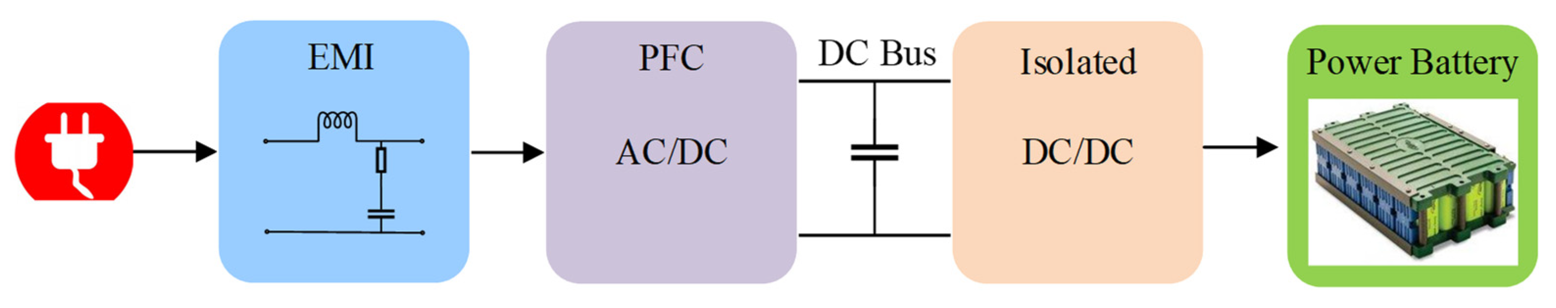
:1. Introduction
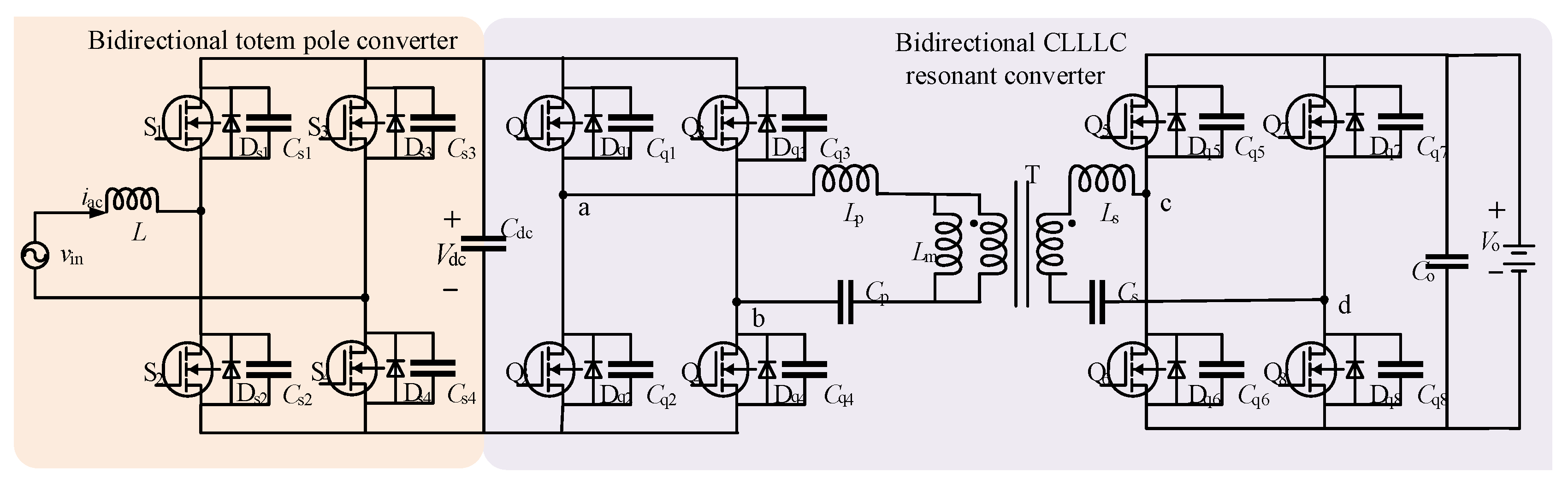
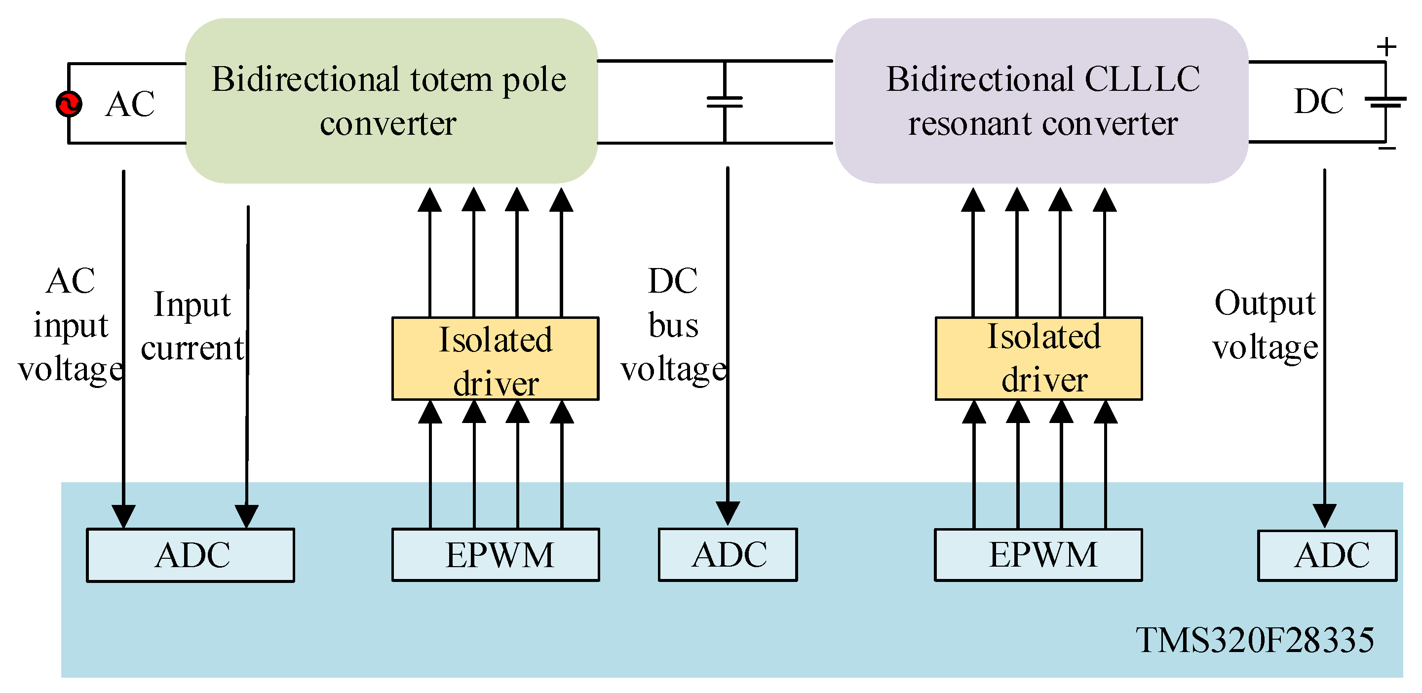
2. Bidirectional Isolation Type Charging System and Characterization
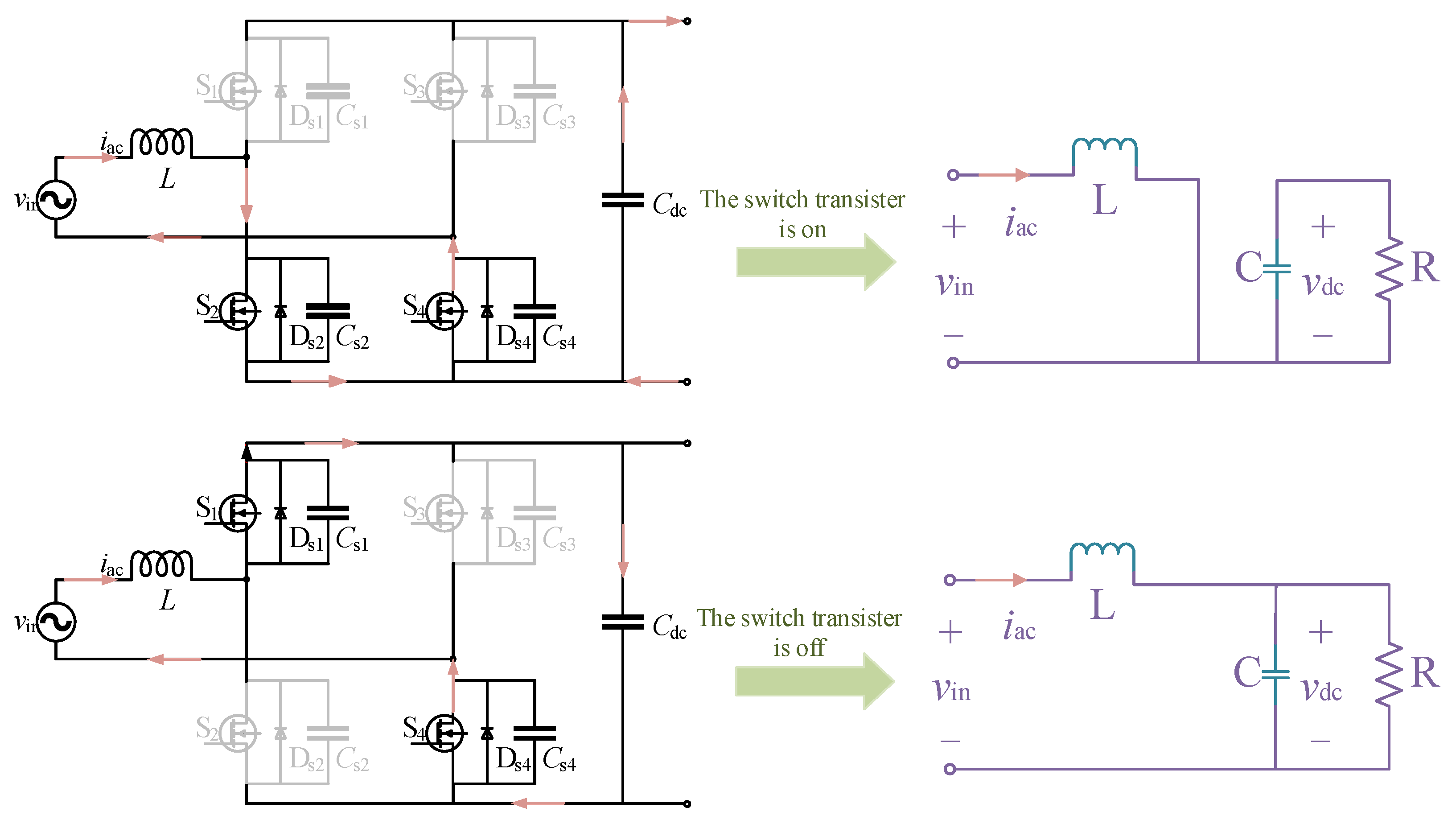
2.1. Modeling Analysis of Bidirectional Totem Pole Converter
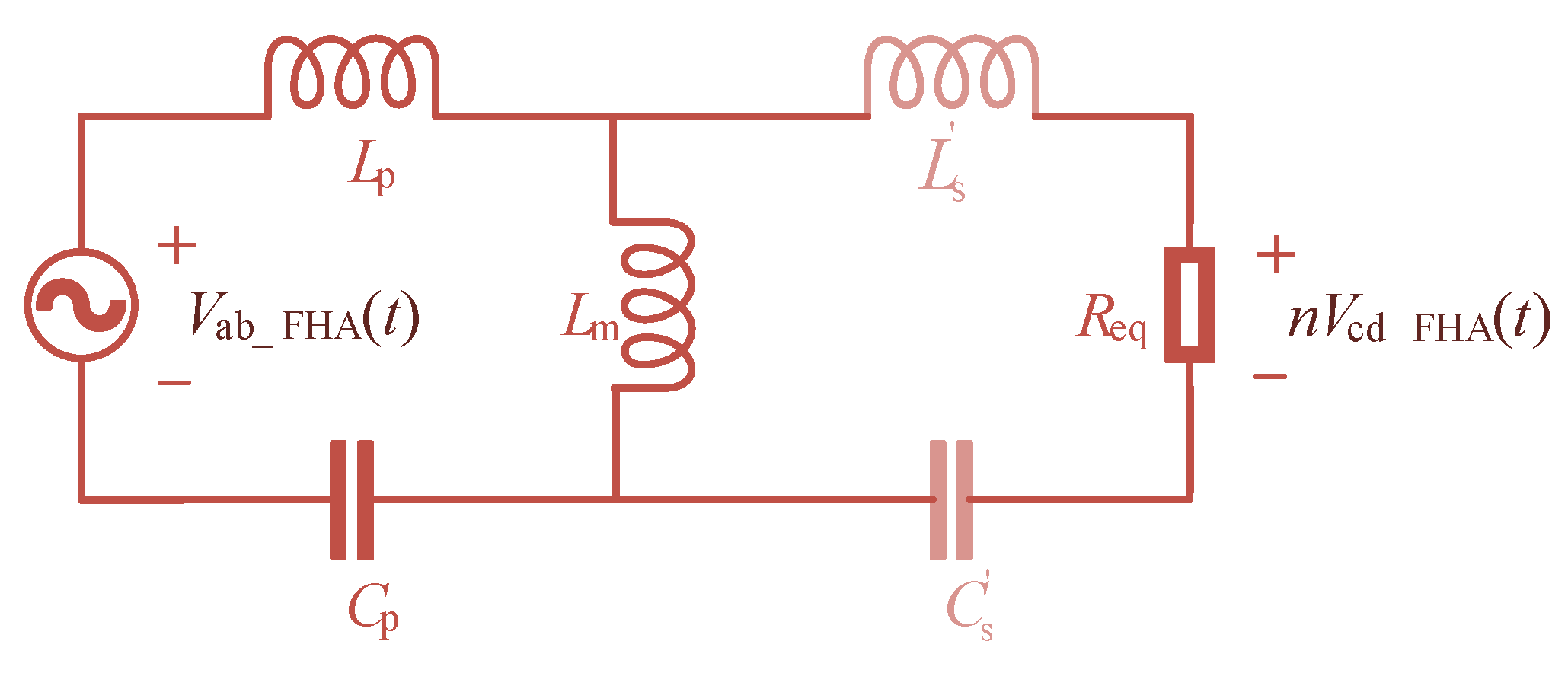
2.2. Bidirectional CLLLC Resonant Converter Modeling
2.2.1. Equivalent Circuit Model
2.2.2. Characteristic Analysis
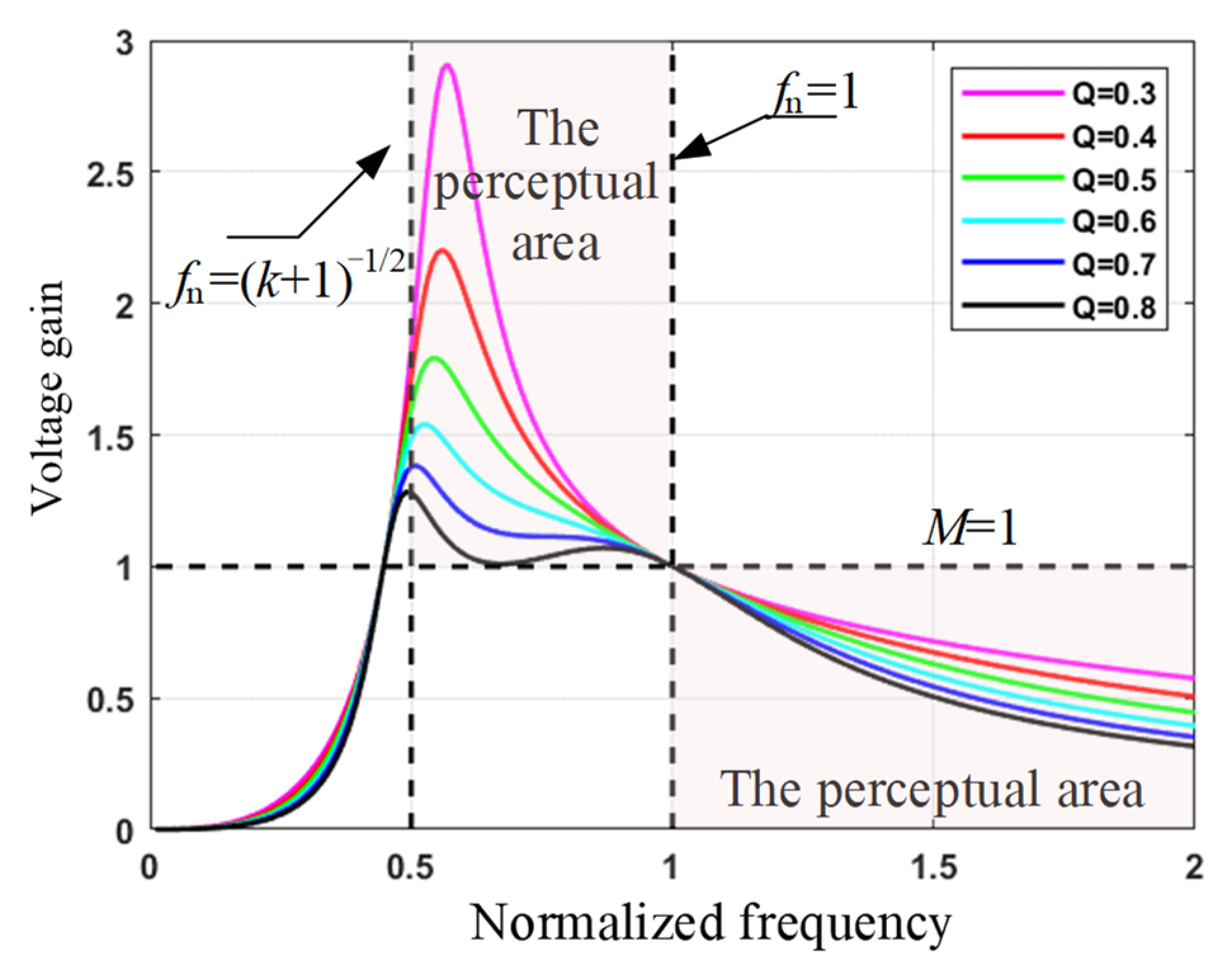
- Voltage Gain Characteristics
- 2.
- Impedance Characteristics Analysis
- 3.
- Design Conditions for the Inductance Factor K and Quality Factor Q
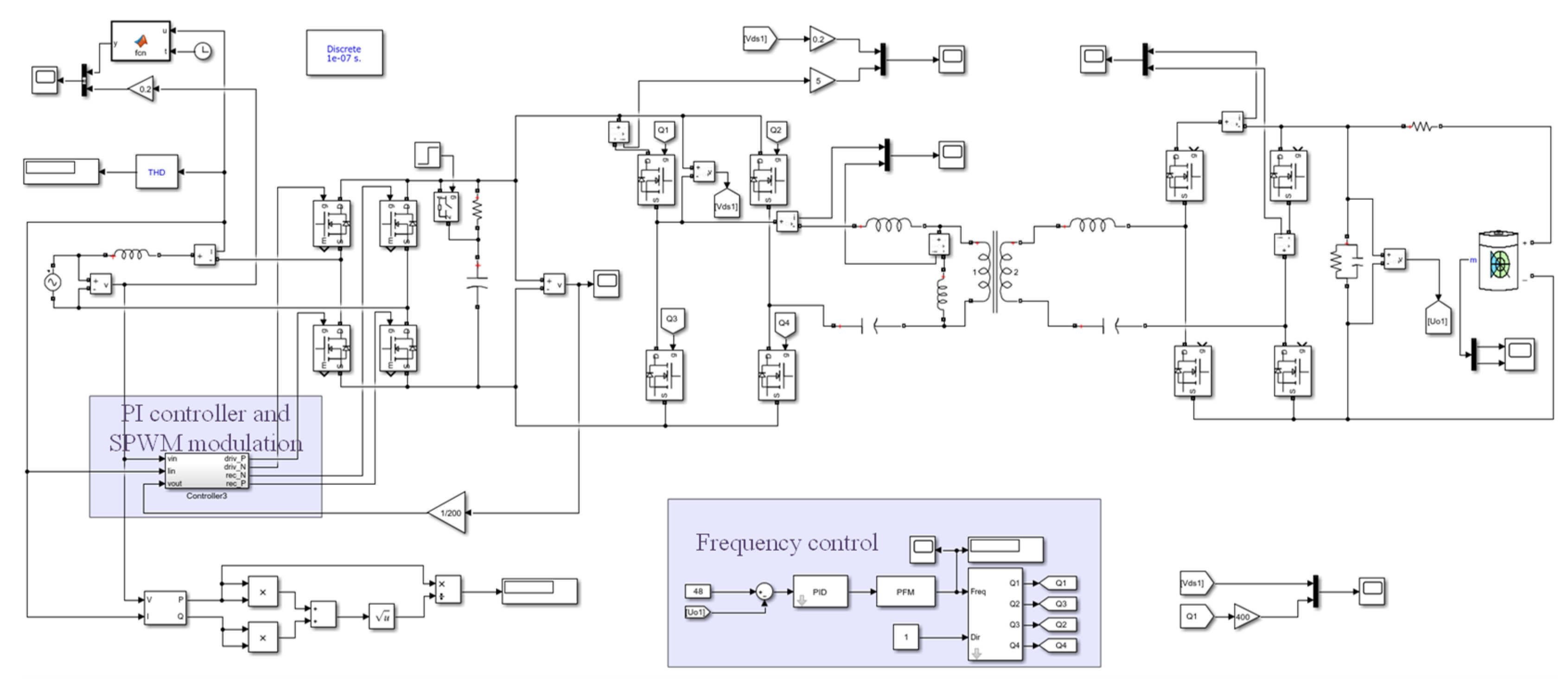
3. Control Strategy of the Charging System
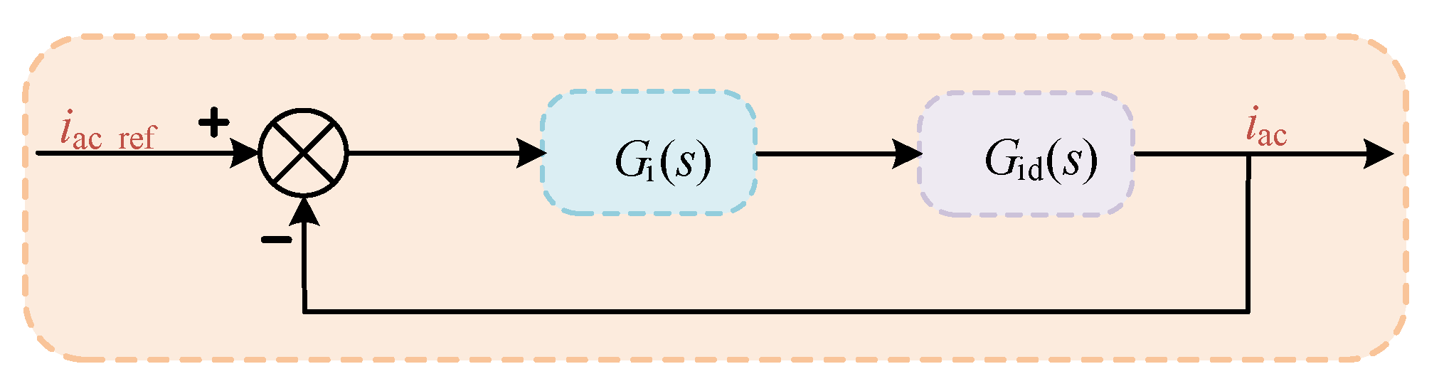
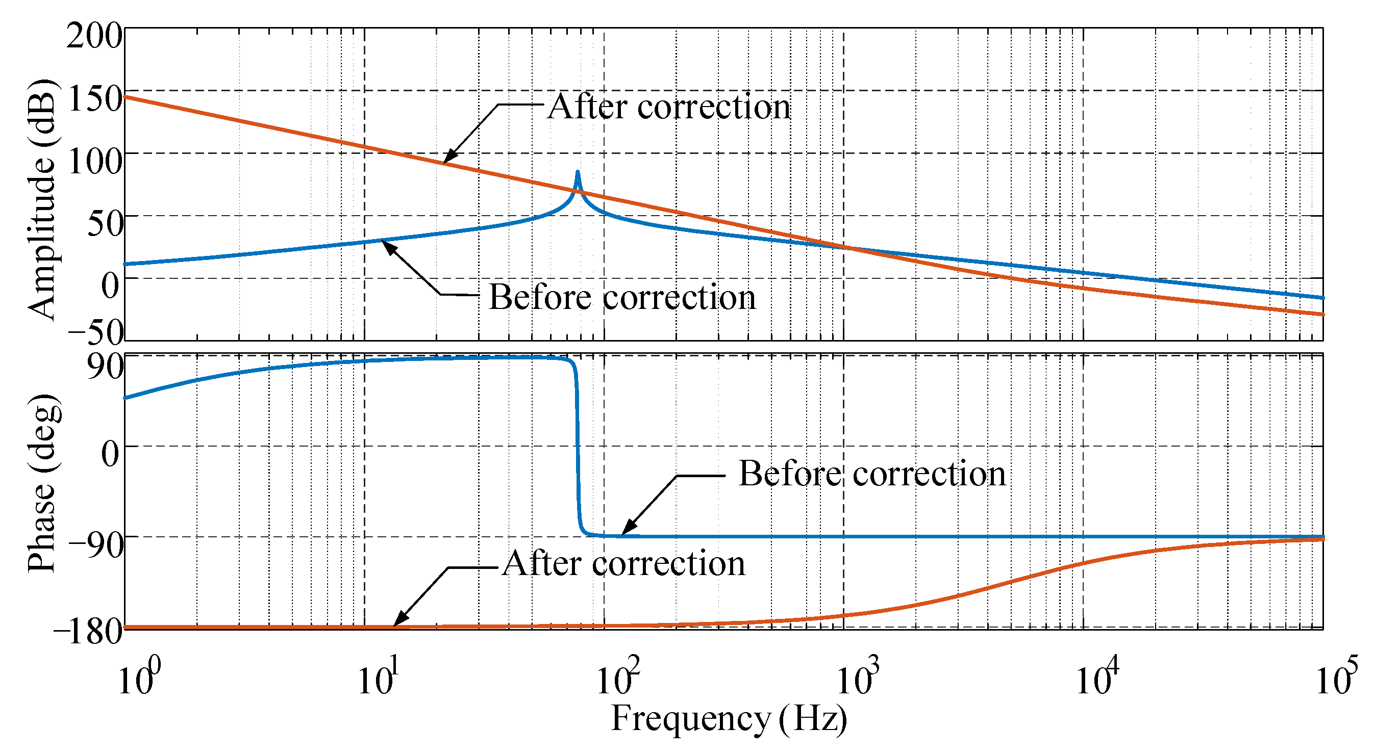
3.1. Current Internal Loop Controller Design
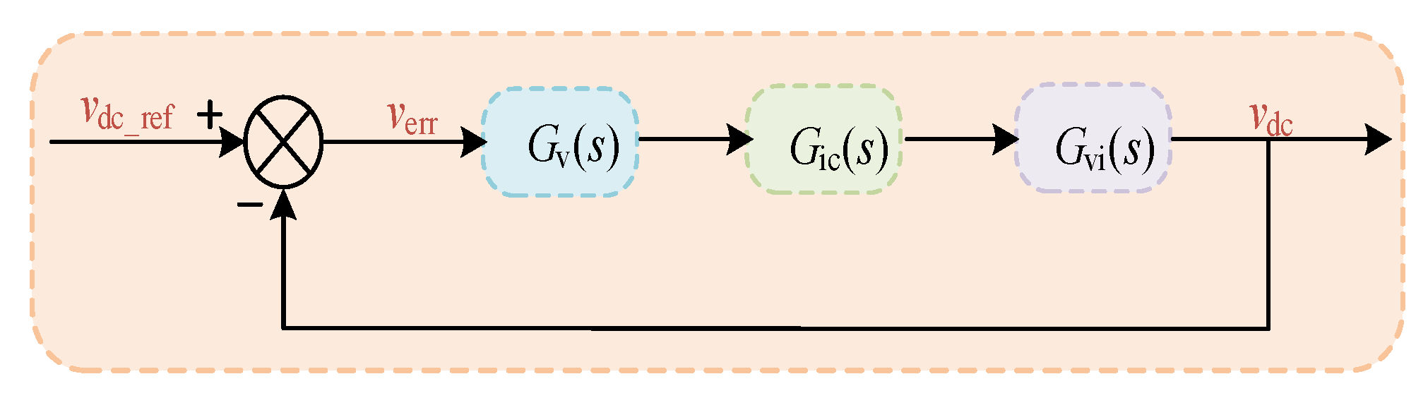
3.2. Voltage Outer Loop Controller Design
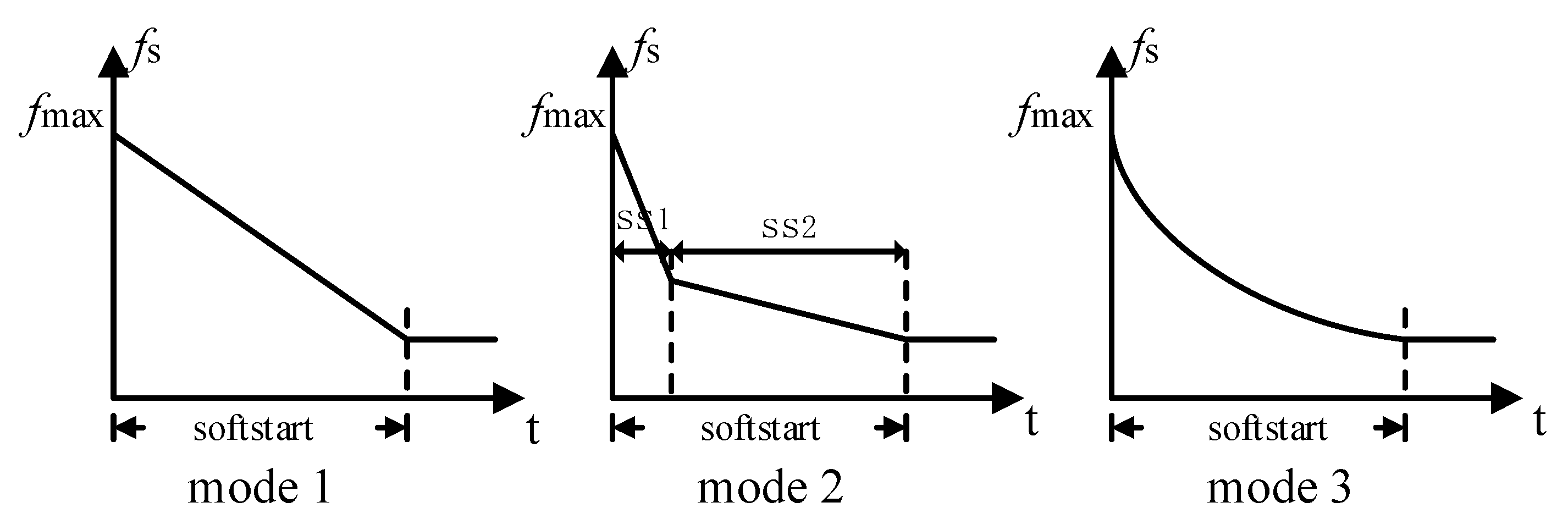
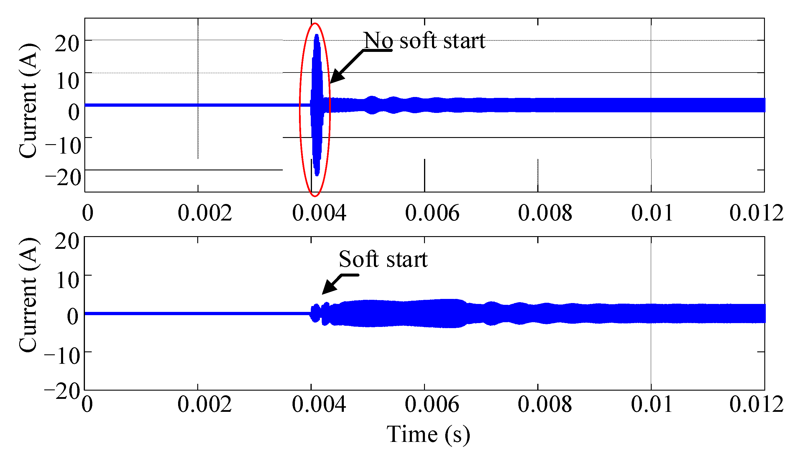
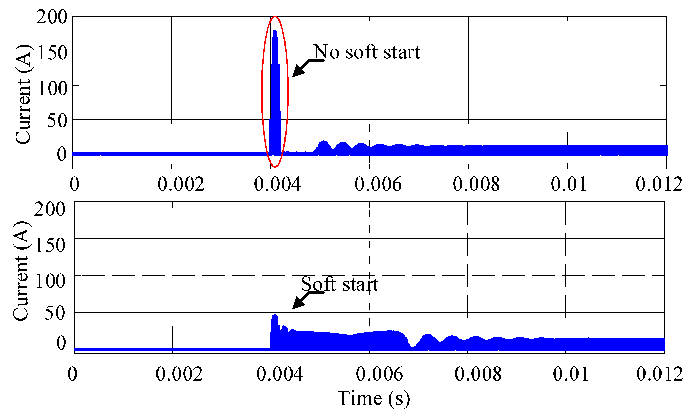
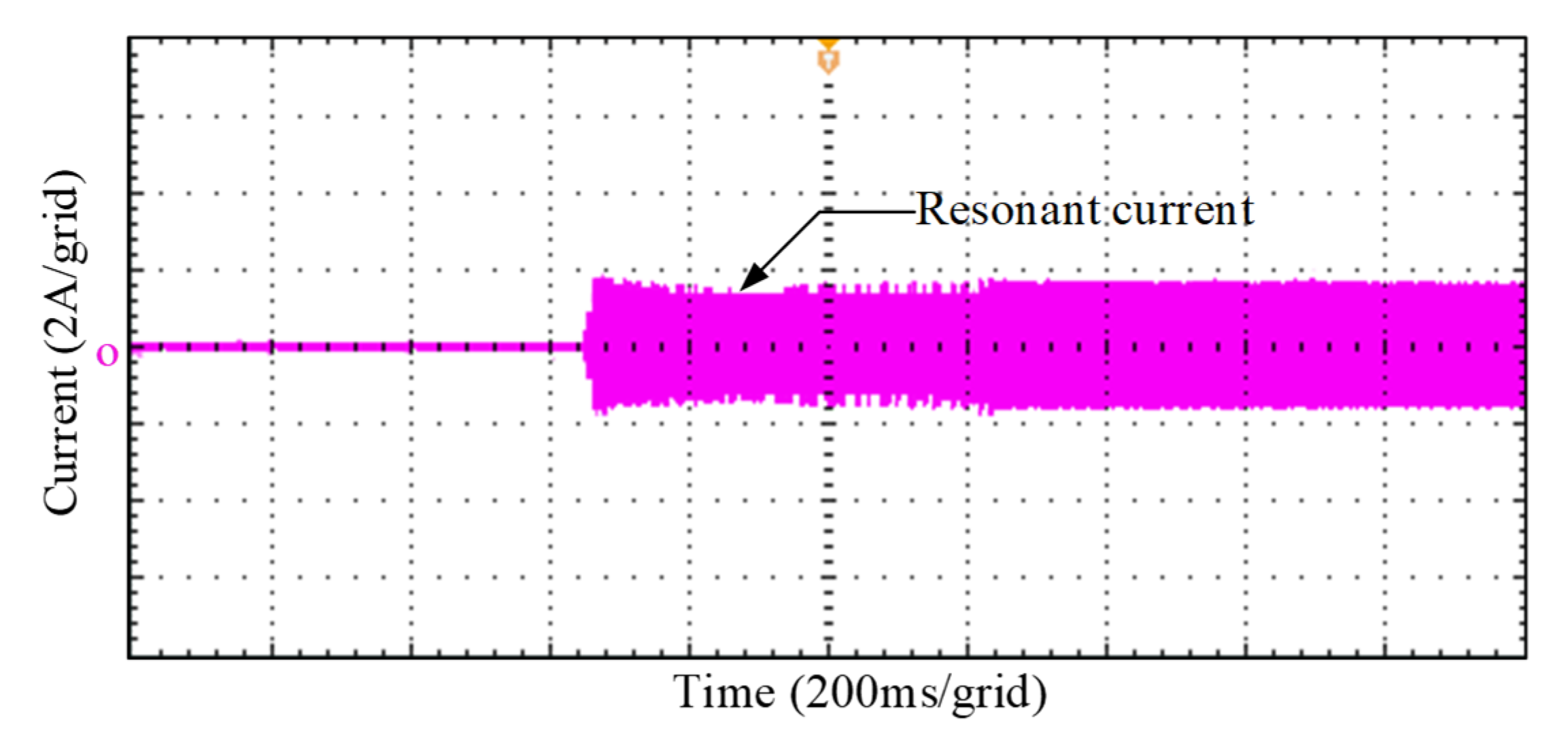
3.3. Control of Soft Start
4. Parameter Design of Charging System
4.1. Parameter Design of Bidirectional Totem Pole Changer
- AC Inductance
- 2.
- DC Bus Capacitance
- 3.
- Power Switching Transistor Selection
4.2. Parameter Design of Bidirectional CLLLC Resonant Changer
- Transformer Turns Ratio
- 2.
- The Maximum and Minimum Voltage Gain of the Transformer
- 3.
- Inductance Factor K and Quality Factor Q
- 4.
- Resonant Inductance and Capacitance
- 5.
- The Selection of Power Switching
5. Simulation Analysis
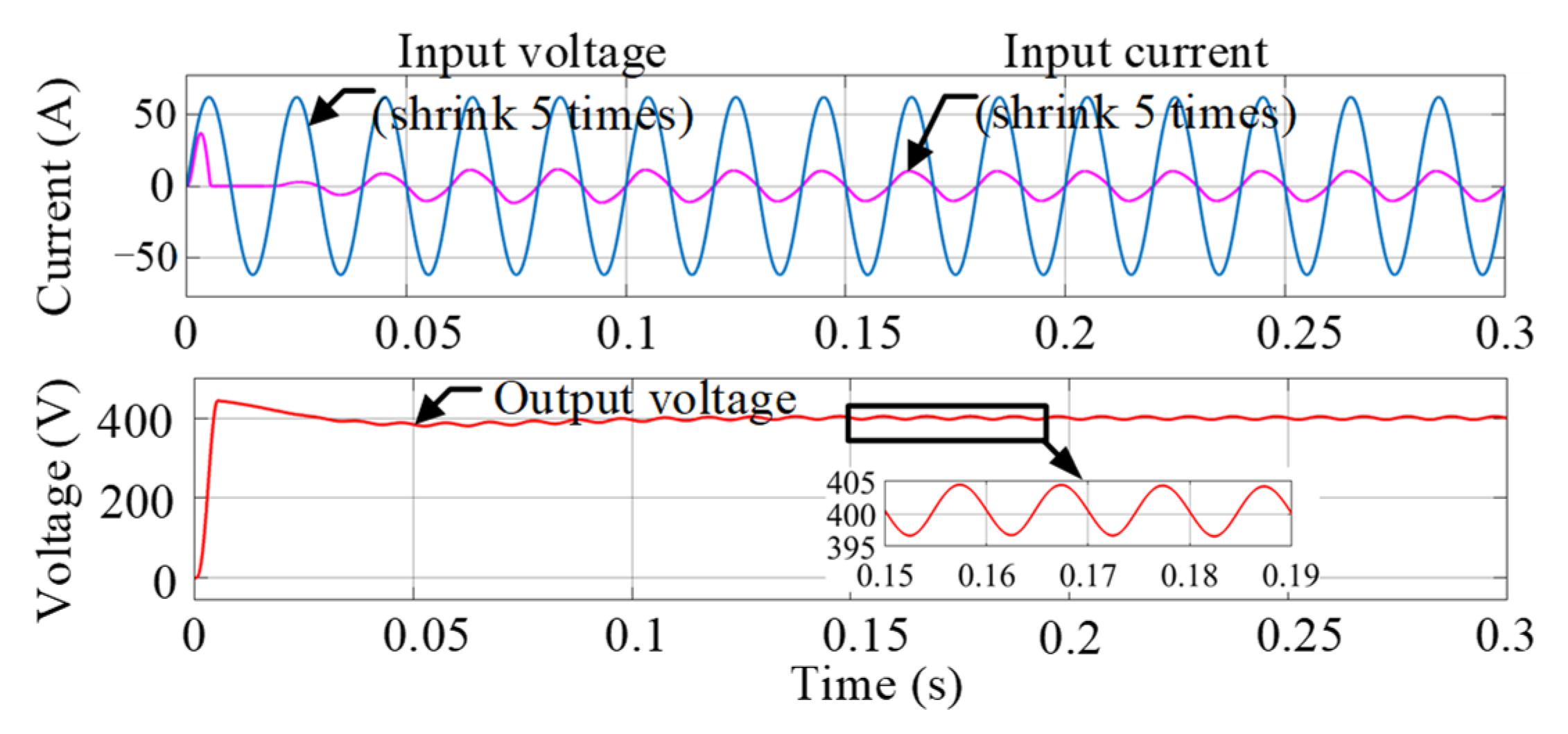
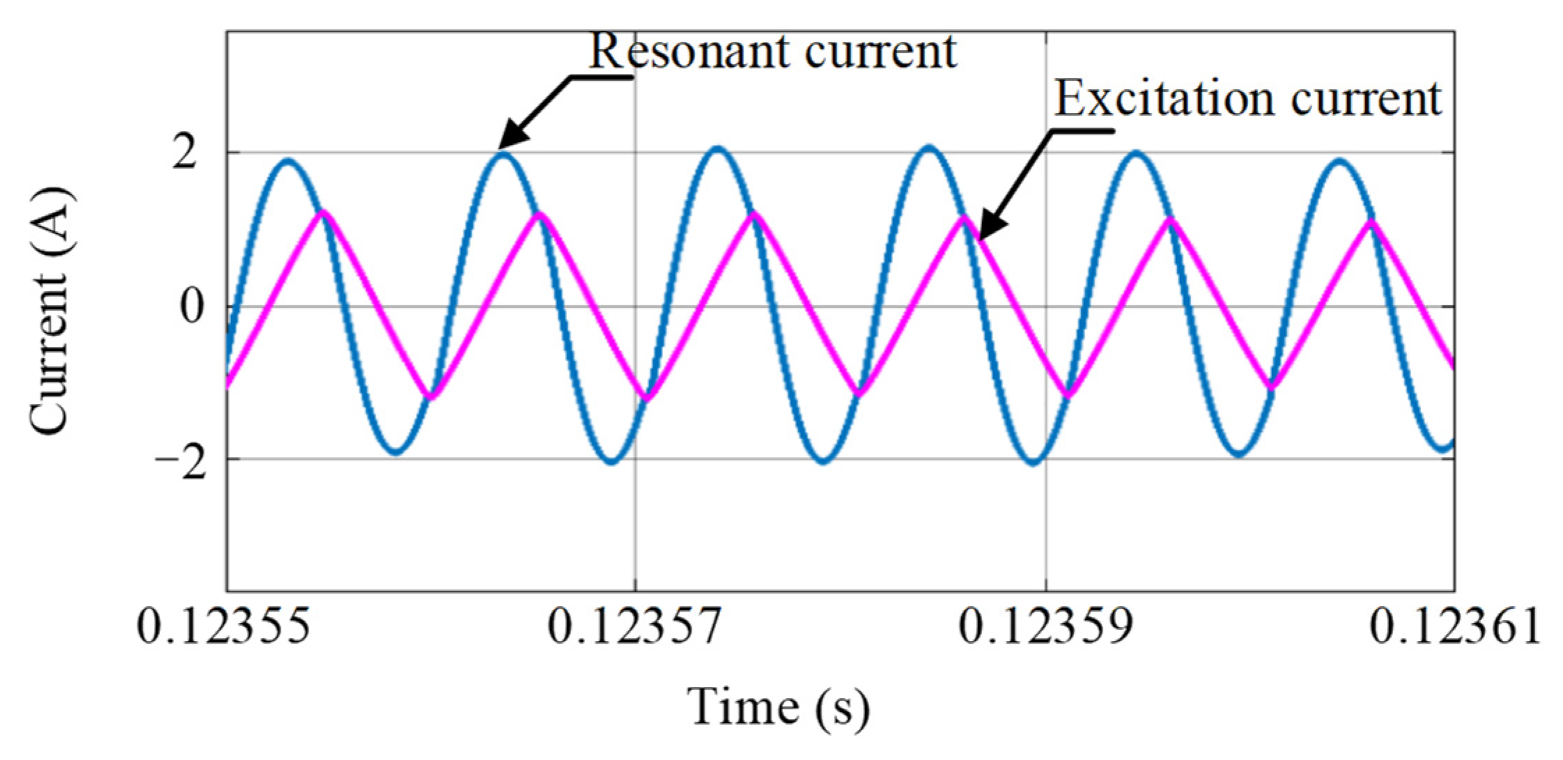
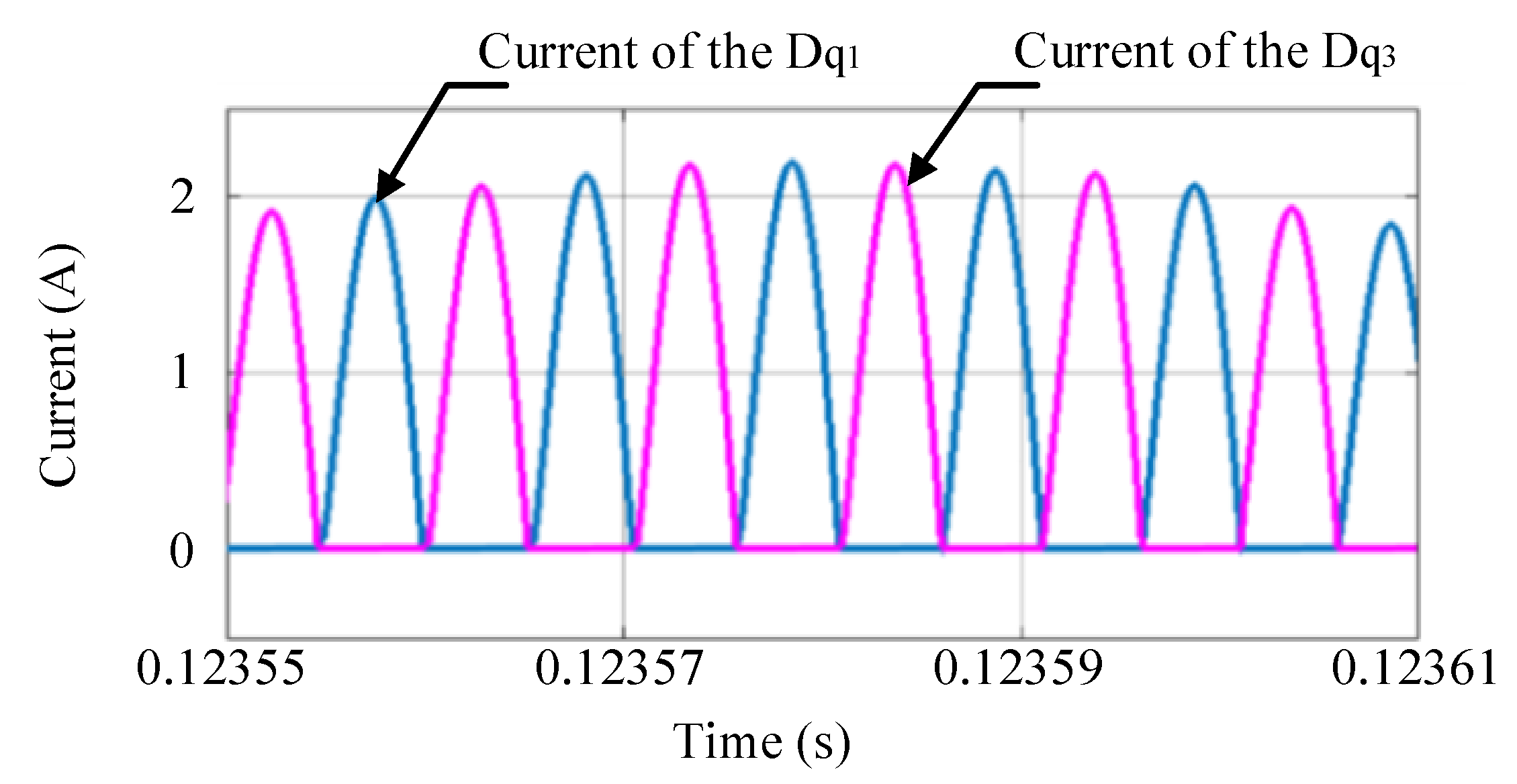
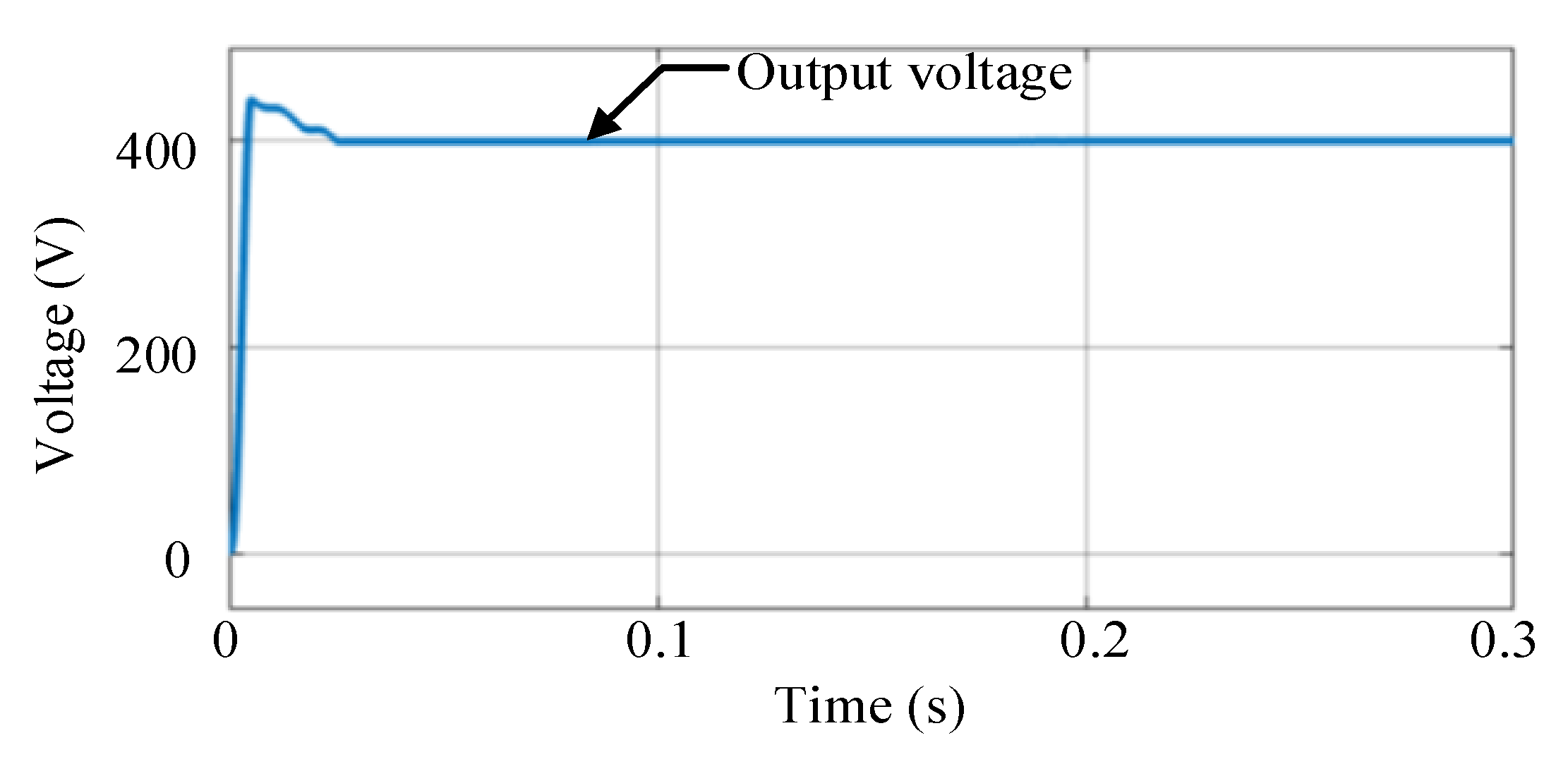
5.1. Simulation of the Forward Operating State
5.2. Simulation of Reverse Operating State
6. Experimental Verification
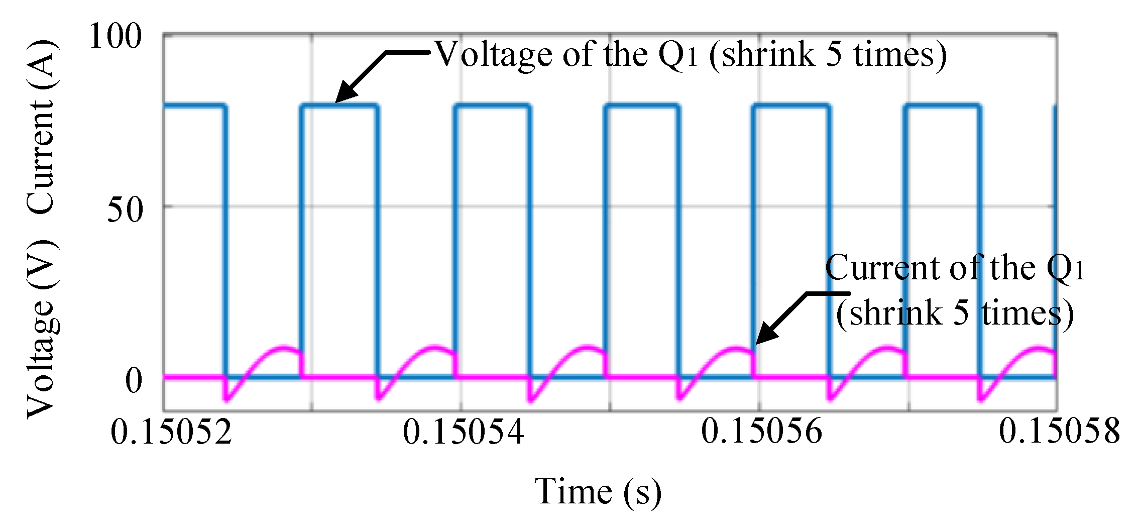
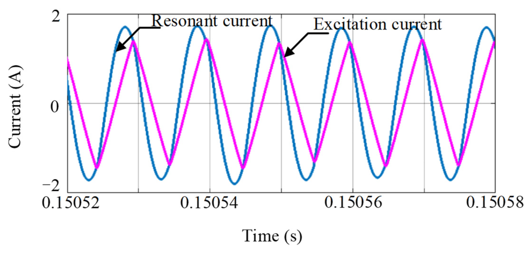
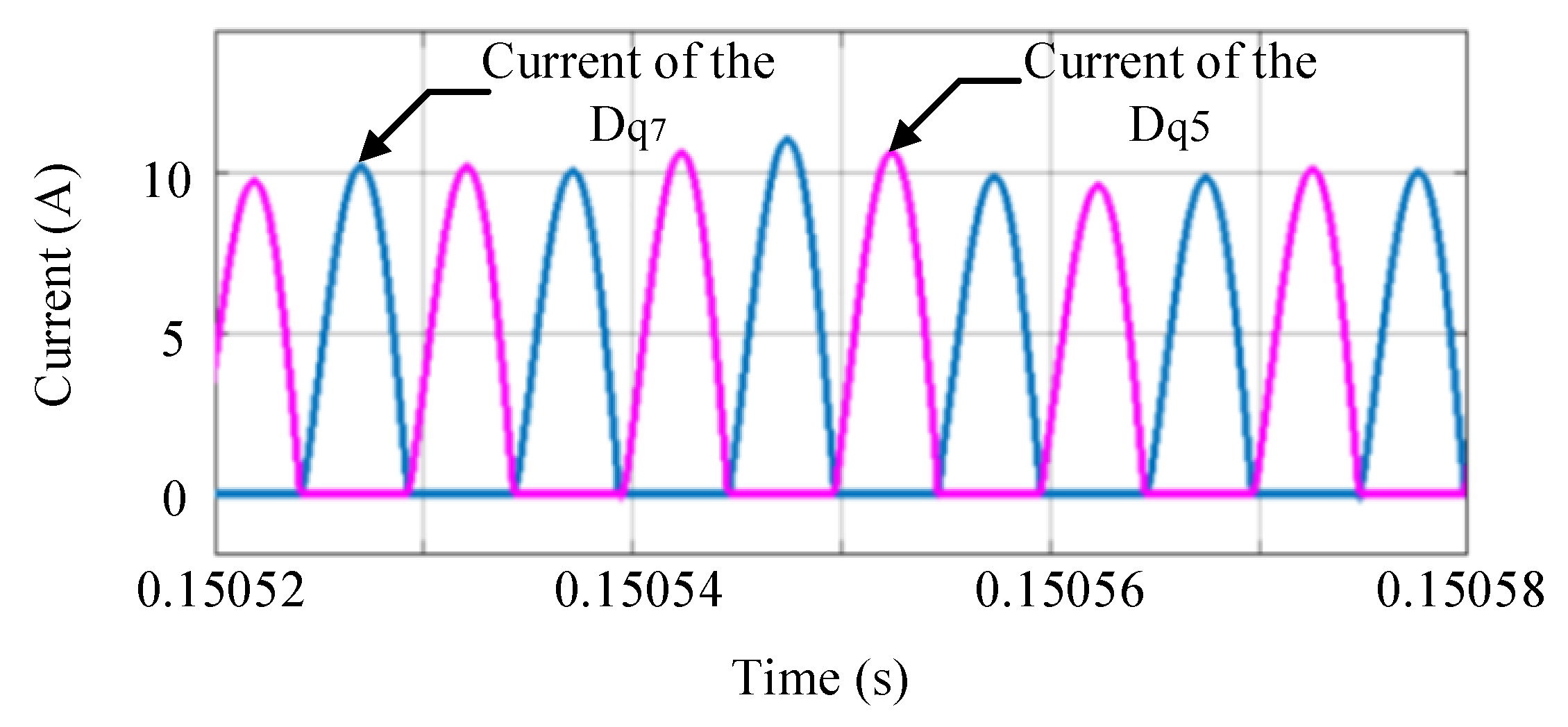
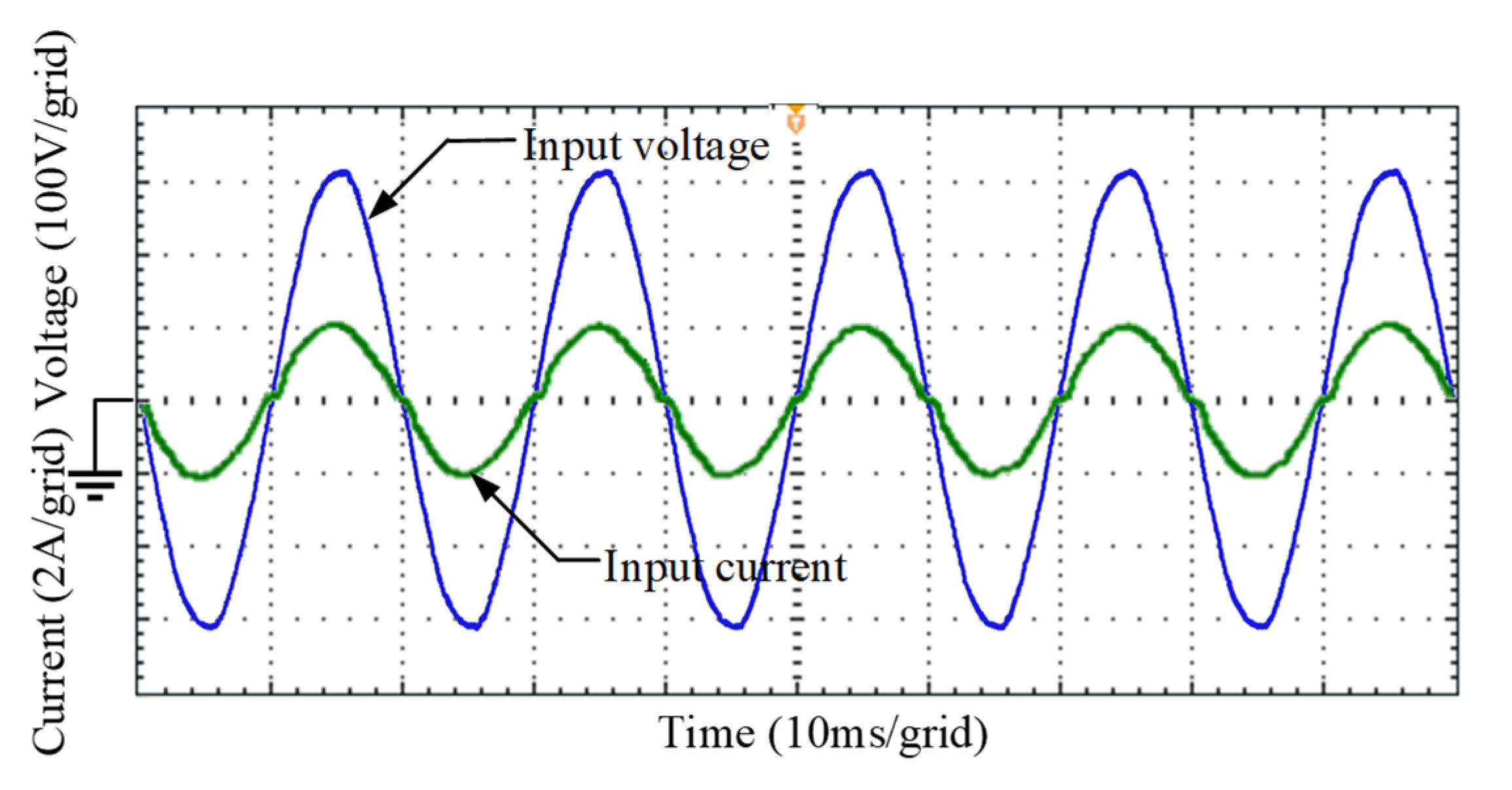
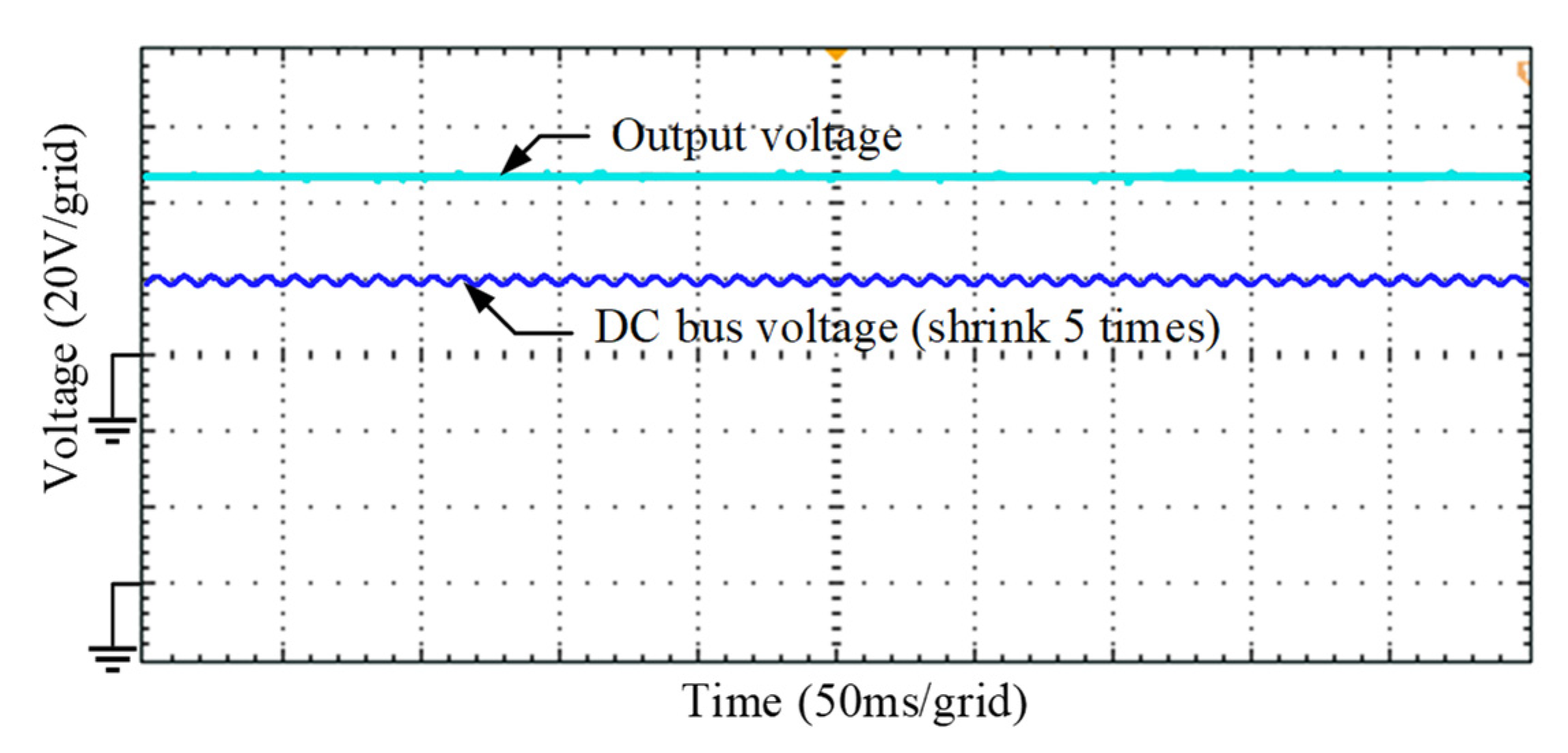
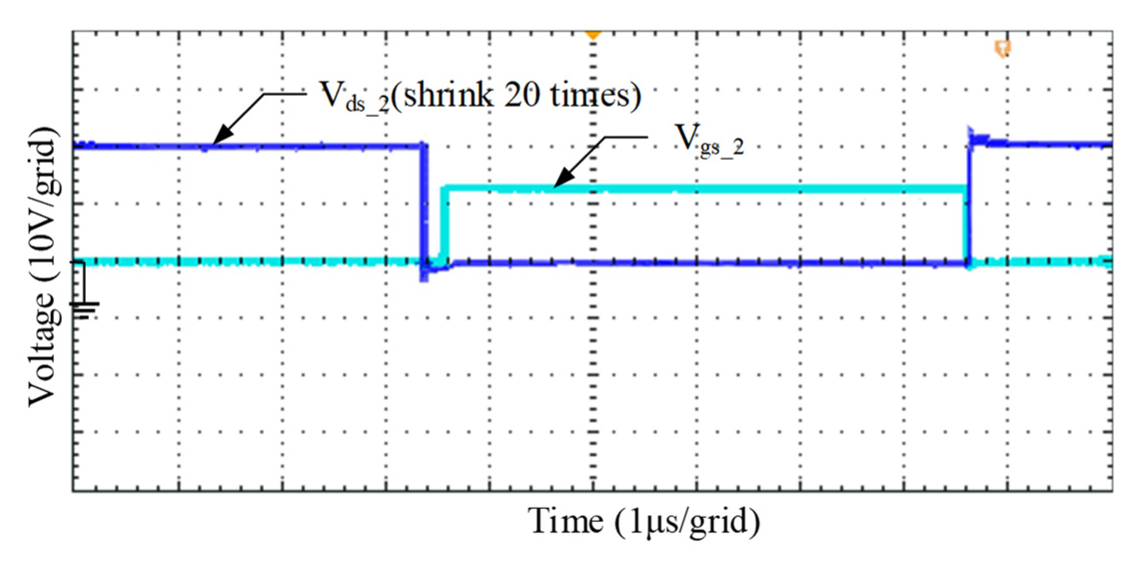
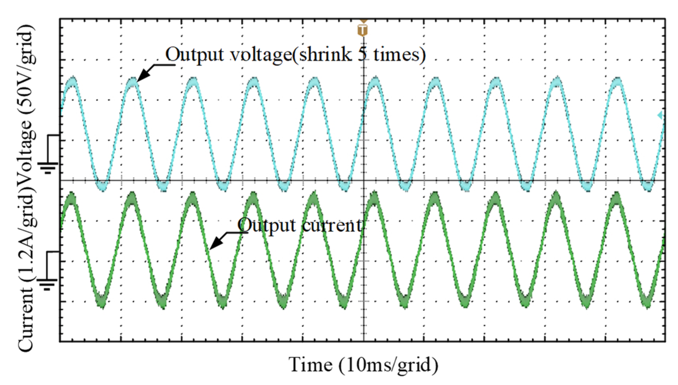
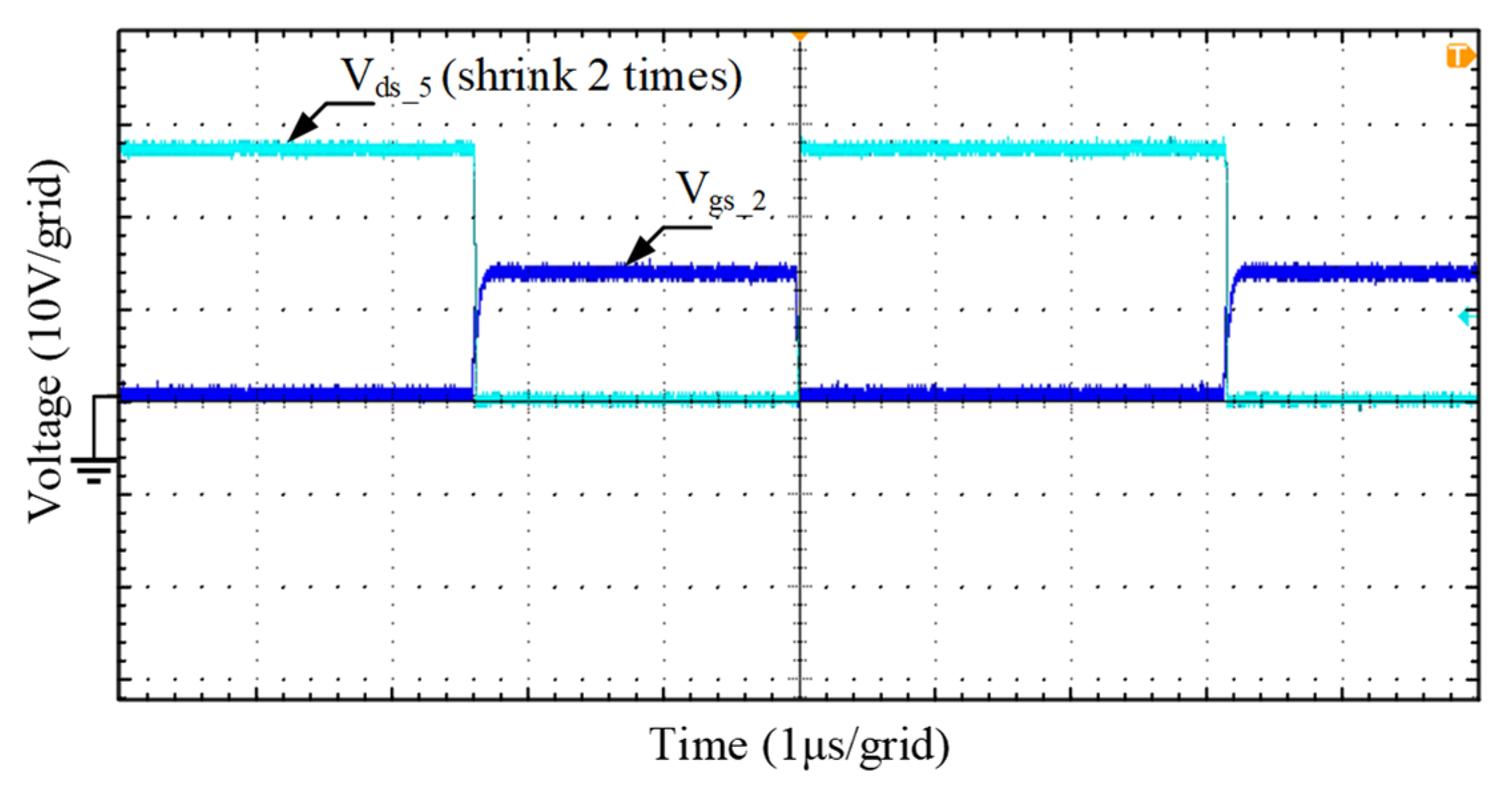
6.1. Forward Operation
6.2. Reverse Operation
7. Conclusions
- Mathematical modeling of bidirectional totem pole converter using small signal analysis can obtain the transfer function of input current transformation with a duty cycle; an equivalent model of a bidirectional CLLLC resonant converter is obtained by fundamental wave analysis for characterization, and the parameters of the design are reasonable.
- The front stage adopts voltage and current double closed-loop control to keep the DC bus voltage stable, and the rear stage adopts frequency conversion and a high-frequency soft start to control the constant output voltage. The simulation model results of the control system show that the control strategy designed in this paper is reasonable.
- The experimental results prove that the bidirectional charging system can achieve power factor correction and has soft switching characteristics across the full load range.
Author Contributions
Funding
Conflicts of Interest
References
- Schmidt, S. Use of battery swapping for improving environmental balance and price-performance ratio of electric vehicles. eTransportation 2021, 9, 100128. [Google Scholar] [CrossRef]
- Hao, X.; Yuan, Y.; Wang, H.; Ouyang, M. Plug-in hybrid electric vehicle utility factor in China cities: Influencing factors, empirical research, and energy and environmental application. eTransportation 2021, 10, 100138. [Google Scholar] [CrossRef]
- Li, R.; Shi, F. Control and Optimization of Residential Photovoltaic Power Generation System with High Efficiency Isolated Bidirectional DC–DC Converter. IEEE Access 2019, 7, 116107–116122. [Google Scholar] [CrossRef]
- Zong, S.; Fan, G.; Yang, X. Double Voltage Rectification Modulation for Bidirectional DC/DC Resonant Converters for Wide Voltage Range Operation. IEEE Trans. Power Electron. 2019, 34, 6510–6521. [Google Scholar] [CrossRef]
- Tang, Z.; Xia, Z.C.; Huang, G.; Su, H.Y. One Cycle Controlled Bidirectional Half-bridge AC-DC Converter. Electr. Drive. 2017, 47, 29–32. [Google Scholar]
- Chen, H.; Liao, J. Bidirectional Current Sensorless Control for the Full-Bridge AC/DC Converter with Considering Both Inductor Resistance and Conduction Voltages. IEEE Trans. Power Electron. 2014, 29, 2071–2082. [Google Scholar] [CrossRef] [Green Version]
- Belkamel, H.; Hyungjin, K.; Beywongwoo, K.; Shin, Y.; Choi, S. Bidirectional Single-Stage Interleaved Totem-Pole AC-DC Converter with High Frequency Isolation for On-Board EV Charger. In Proceedings of the 2018 IEEE Energy Conversion Congress and Exposition (ECCE), Portland, OR, USA, 23–27 September 2018. [Google Scholar]
- Mei, Y.; Xu, C.; Lu, Q.C. Piecewise Synchronous Control Strategy of Bidirectional Isolated Matrix AC-DC Converter Based on Zero Vector Embedded. Trans. China Electrotech. Soc. 2021, 36, 4784–4794. [Google Scholar]
- Gu, L.; Jin, K.; Zhou, H.L. A Single-stage Three-phase Isolated Bidirectional AC/DC Converter and Its SVPWM Algorithm. Proc. CSEE 2015, 35, 3886–3894. [Google Scholar]
- Zhou, Y.X.; Qin, W.P.; Wang, Q.; Ren, C.G.; Han, X.Q. A Dual-phase-shift Plus Frequency Control Strategy of Isolated Bidirectional AC/DC Converter. Power Sys. Technol. 2019, 43, 1826–1833. [Google Scholar]
- Zhang, G.R.; Ma, C.; Yu, Y.Q.; Xiao, X.F. Analysis and Design of Current Loop of Diode-clamped Three-level Active Power Filter. Elec. Meas. Instrum. 2016, 53, 93–99. [Google Scholar]
- Xu, C. Research on Optimal Design of High Frequency Transformer for Bidirectional Isolated AC-DC Matrix Converter. Master’s Thesis, North China University of Technology, Beijing, China, 2022. [Google Scholar]
- Gao, N.; Zhang, Y.; Guan, Q.X.; Qiu, Z.G. Five-level Active Neutral Point Clamed Dual Active Bridge DC/DC Converter. Proc. CSEE 2022, 1, 13. [Google Scholar]
- Guo, H.Y.; Zhang, X.W.; Zhao, G.; Gao, S. Minimum Current Stress Optimization for Dual Active Bridge DC/DC Converters. Power Electron. 2019, 53, 120–122. [Google Scholar]
- Yang, Y.Y. Research and Design of Rectification/Inverter Bidirectional Converter in Bidirectional OBC. Master’s Thesis, Zhejiang University, Hangzhou, China, 2018. [Google Scholar]
- Kim, J.; Park, M.; Lee, B.; Lai, J. Analysis and Design of LLC Converter Considering Output Voltage Regulation Under No-load Condition. IEEE Trans. Power Electron. 2020, 35, 522–534. [Google Scholar] [CrossRef]
- Liu, J.Q.; Zhao, N.; Sun, C.B.; Wang, Y.; Qi, H.F. Research on Control Strategy of Power Electronic Traction Transformer Based on LLC Resonant Converter. Trans. China Electrotech. Soc. 2019, 34, 3333–3334. [Google Scholar]
- Li, J.J.; Wu, H.F.; Hua, W.M. Matrix Inductor-transformer Integration and Optimization Design for CLLC Bidirectional Resonant Converter. Proc. CSEE 2022, 42, 3720–3729. [Google Scholar]
- Li, P.C.; Zhang, J.C.; Kan, C.Z.; Fen, B. An Integrated Buck-Boost CLLC Bidirectional DC Converter with High Gain and Soft Switching. Proc. CSEE 2018, 38, 3295–3305. [Google Scholar]
- Li, S.C.; Liu, B.Y.; Jiang, Q.; Duan, S.X. Performance Analysis of Bidirectional CLLLC Resonant Converter with Synchronous PWM Control Strategy. Trans. China Electrotech. Soc. 2019, 34, 5543–5552. [Google Scholar]
- Chen, Q.C.; Ji, Y.C.; Wang, J.J. Analysis and Design of Bidirectional CLLLC Resonant DC-DC Transformers. Proc. CSEE 2014, 34, 2898–2905. [Google Scholar]
- Li, H.; Zhang, Z.; Wang, S.; Tang, J.; Ren, X.; Chen, Q. A 300-kHz 6.6-kW SiC Bidirectional LLC On-Board Charger. IEEE Trans. Ind. Electron. 2020, 67, 1435–1445. [Google Scholar] [CrossRef]
- Tao, W.D.; Wang, Y.B.; Zhang, F.Y.; Qu, Z.B.; Pan, T.T. Pulse Frequency Modulation and Phase Shift Combined Control Method for Bidirectional LLC Resonant Converter. Trans. China Electrotech. Soc. 2018, 33, 5856–5863. [Google Scholar]
- Wang, X.S. Research of Half-Bridge Three-Level Bidirectional LLC Resonant Converter. Master’s Thesis, Hefei University of Technology, Hefei, China, 2019. [Google Scholar]
- Qu, L.; Wang, X.; Xu, J.Y.; Liu, H. Design method of bidirectional CLLC resonant converter for on-board charger applications. J. HIT. 2021, 53, 144–155. [Google Scholar]
- Wang, X.Y.; Wei, X.Z.; Zhu, J.G.; Dai, H.F.; Zheng, Y.J.; Xu, X.M.; Chen, Q.J. A review of modeling, acquisition, and application of lithium-ion battery impedance for onboard battery management. eTransportation 2021, 7, 100093. [Google Scholar] [CrossRef]
- Shi, B.K.; Yang, F.Y.; Hu, C.; Ouyang, M.G. Modelling and improvement of oscillation problem in a double-sided LCC compensation network for electric vehicle wireless power transfer. eTransportation 2021, 8, 100108. [Google Scholar] [CrossRef]
- Chen, Q.C.; Wang, Y.Z.; Ji, Y.C. Control Scheme of Bidirectional LLC Resonant DC-DC Transformer for Soft Start and Power Conversion. Trans. China Electrotech. Soc. 2014, 29, 180–186. [Google Scholar]
- Li, Y.D. Research on Bidirectional Symmetric CLLLC Resonant Energy Storage Converter. Master’s Thesis, Beijing Jiaotong University, Beijing, China, 2021. [Google Scholar]
- Wang, H.X. Design and Research of Bidirectional DC/DC Resonate Converter Applied to On-Board Charger. Master’s Thesis, Zhejiang University, Hangzhou, China, 2018. [Google Scholar]
- Luo, Y.W.; Qian, Y.P.; Zeng, Z.Z.; Zhang, Y.J. Simulation and analysis of operating characteristics of power battery for flying car utilization. eTransportation 2021, 8, 100111. [Google Scholar] [CrossRef]


| Symbol | Description | Value |
|---|---|---|
| Vin | AC input voltage range | 176–264 V |
| Vin_rated | Rated AC side input voltage | 220 V |
| Vdc | DC bus voltage range | 380–420 V |
| Vdc_rated | Rated DC bus voltage | 400 V |
| Vo | DC output voltage range | 44–56 V |
| Vo_rated | Rated DC output voltage | 48 V |
| Po | Rated power | 300 W |
| fs | Switching frequency | 50–150 kHz |
| fr1 | Resonant frequency | 100 kHz |
| η | Efficiency | 95% |
Publisher’s Note: MDPI stays neutral with regard to jurisdictional claims in published maps and institutional affiliations. |
© 2022 by the authors. Licensee MDPI, Basel, Switzerland. This article is an open access article distributed under the terms and conditions of the Creative Commons Attribution (CC BY) license (https://creativecommons.org/licenses/by/4.0/).
Share and Cite
Zhou, K.; Sun, Y. Research on Bidirectional Isolated Charging System Based on Resonant Converter. Electronics 2022, 11, 3625. https://doi.org/10.3390/electronics11213625
Zhou K, Sun Y. Research on Bidirectional Isolated Charging System Based on Resonant Converter. Electronics. 2022; 11(21):3625. https://doi.org/10.3390/electronics11213625
Chicago/Turabian StyleZhou, Kai, and Yue Sun. 2022. "Research on Bidirectional Isolated Charging System Based on Resonant Converter" Electronics 11, no. 21: 3625. https://doi.org/10.3390/electronics11213625