1. Introduction
The power amplifier is a type of electronic amplifier designed to increase the magnitude of the power of a given input signal. The audio power amplifier circuit is an essential branch of the power amplifier, one of the essential components of a sound system. It is designed as a final block in an audio amplifier chain to increase the input signal to a level that is high enough to drive loads. It has come a long way under the influence of the rapid development of integrated circuits in recent decades.
The audio power amplifier market is driven by the increasing demand for mobile audio devices, the growing prevalence of consumer electronics devices worldwide, the growing appeal of in-car infotainment systems, and the growing market for high-quality audio devices. According to the report by [
1], “The audio amplifier market size is expected to grow from USD 3.4 billion in 2019 to USD 4.4 billion by 2024, at a CAGR of 5.6% from 2019 to 2024”. A larger market makes upgrading and improving audio amplifiers very meaningful.
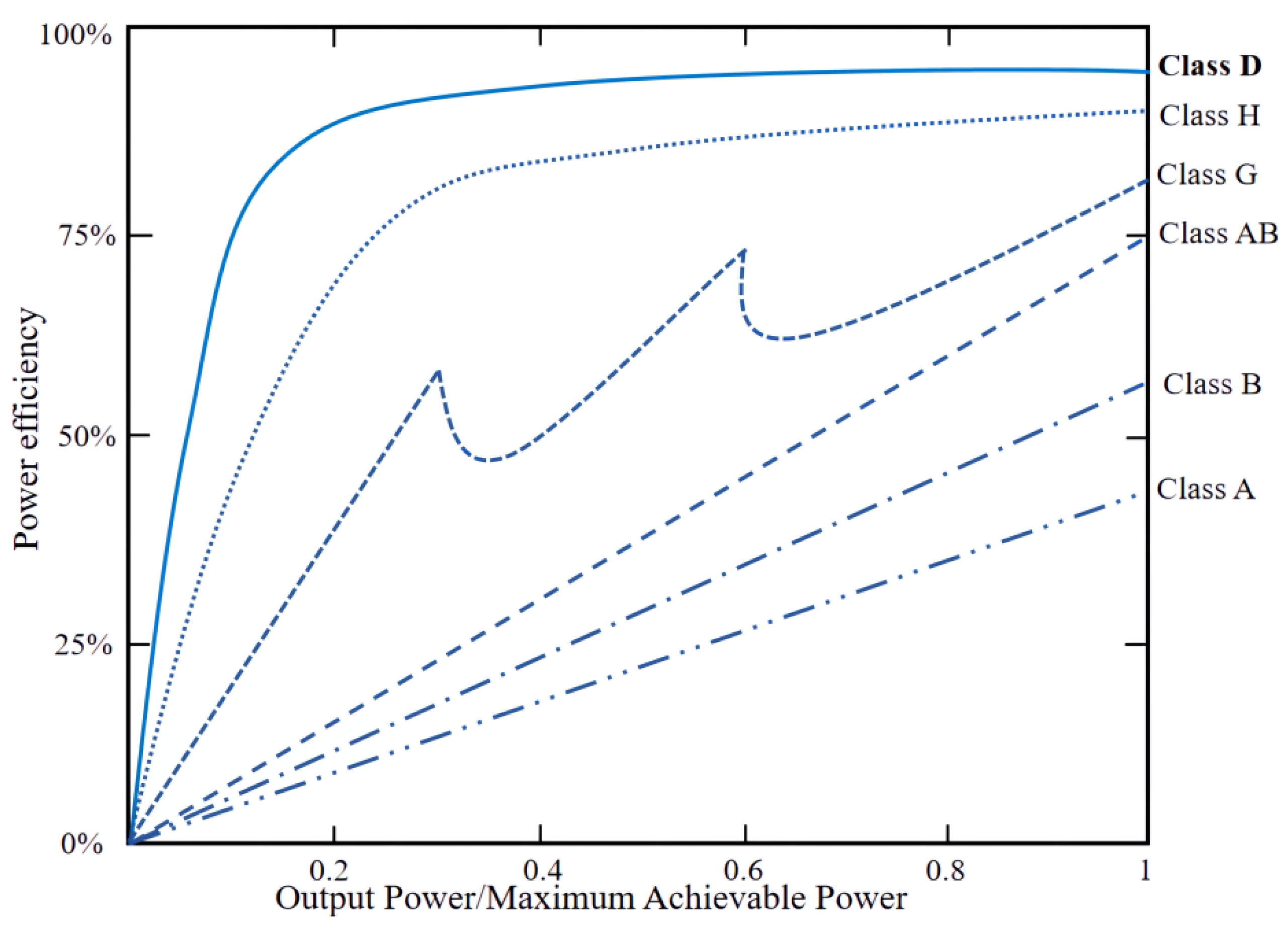
The power efficiency comparison of audio amplifiers is shown in
Figure 1. Traditional analog power amplifiers can be classified into Class A, Class B, Class AB, and other forms according to different working conditions. These kinds of amplifiers have high fidelity, which means they can provide superior sound quality. However, the power conversion efficiency of linear and non-linear amplifiers is extremely low. The emergence of Class D amplifiers solves this problem. The Class D amplifier was first devised in 1958 [
2]. Compared to linear power amplifiers (Class A) and non-linear amplifiers (Class AB, Class B, Class C) [
3,
4], the primary advantage of switching-type Class D amplifiers is their theoretical 100% power efficiency [
5]. The power efficiency of Class D amplifiers at a maximum modulation index is typically higher than 90% [
6]. In contrast, the power efficiency of linear amplifiers such as Class B and Class AB power amplifiers was only 70% or less. This is why the Class D amplifier is currently the best choice for commercial audio amplifiers and is gradually replacing linear counterparts [
7].
The switching device in the output stage is the main point in the history of Class D amplifier development. Germanium transistors were a part of early Class D amplifier design but proved unsuitable for switching topology, hence, early amplifier designs were unsuccessful. Nevertheless, thanks to the advent of MOSFET technology, the relative technology of Class D design was again developed by engineers. The Class D amplifier is currently widely used in various fields such as flat-screen televisions and car sound-control units. Class D amplifiers use a pair of switching devices for push/pull configuration.
The performance of the switching device directly affects the power efficiency and high fidelity of the audio system. Due to the limitation of material characteristics, it is difficult to improve the overall performance of existing silicon-based devices by improving the device structure and manufacturing process [
5,
10]. Therefore, new high-performance power devices are needed as substitutes to achieve better conversion efficiency, which requires minor conduction and lower switching losses to suit variable frequency occasions.
The primary purpose of this paper is to review the basic design of Class D audio amplifiers and propose the research direction for future amplifiers. This paper consists of six sections.
Section 2 reviews the topology and performance of the Class D amplifier.
Section 3 focuses on the Class D power amplifier modulation strategies and reviews its design scheme.
Section 4 introduces the advantages and disadvantages of Class D amplifiers based on GaN devices.
Section 5 and
Section 6 are the discussion and conclusion, respectively.
2. Topologies for Class D Amplifiers
The amplifier’s topologies are the basic structure that depends on the work mode and parameters such as power efficiency and degree of distortion. This paper analyzes the Class D amplifier’s topological model to determine the advantages and disadvantages, lists standard amplifier design examples, and provides the basis for improving the amplifier.
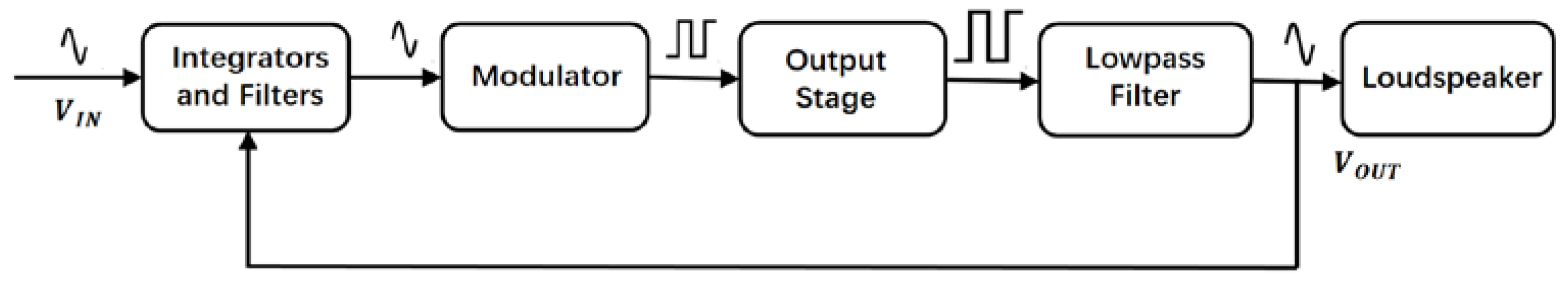
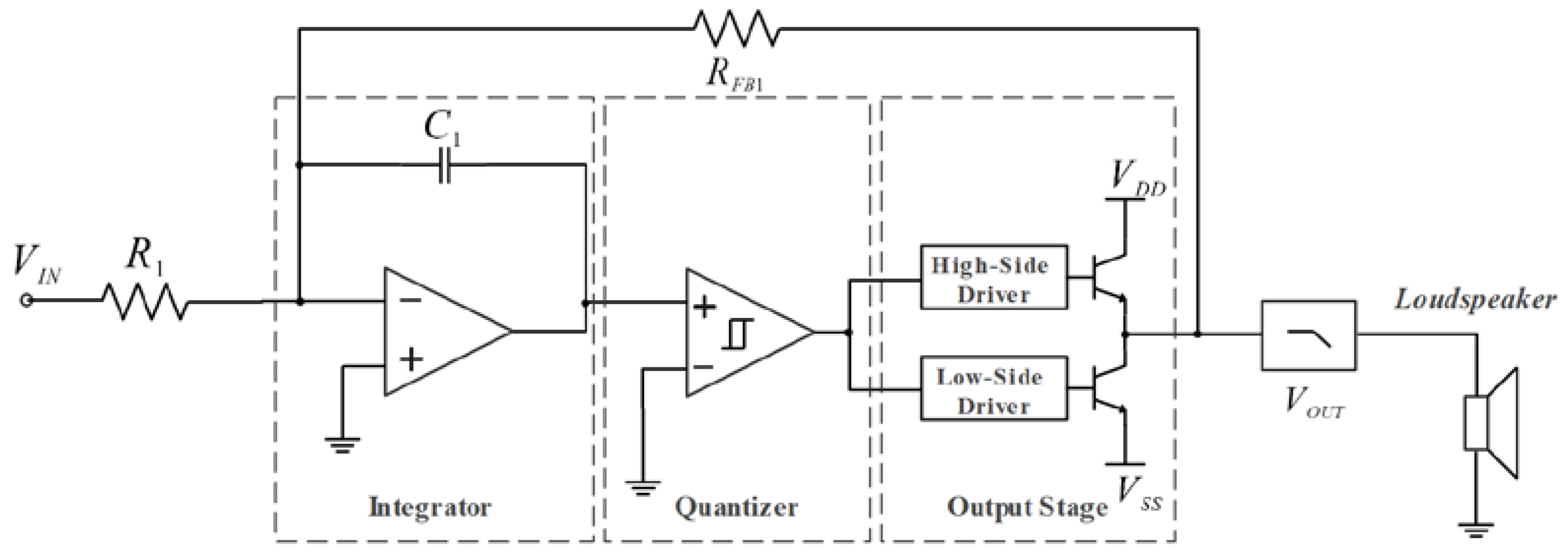
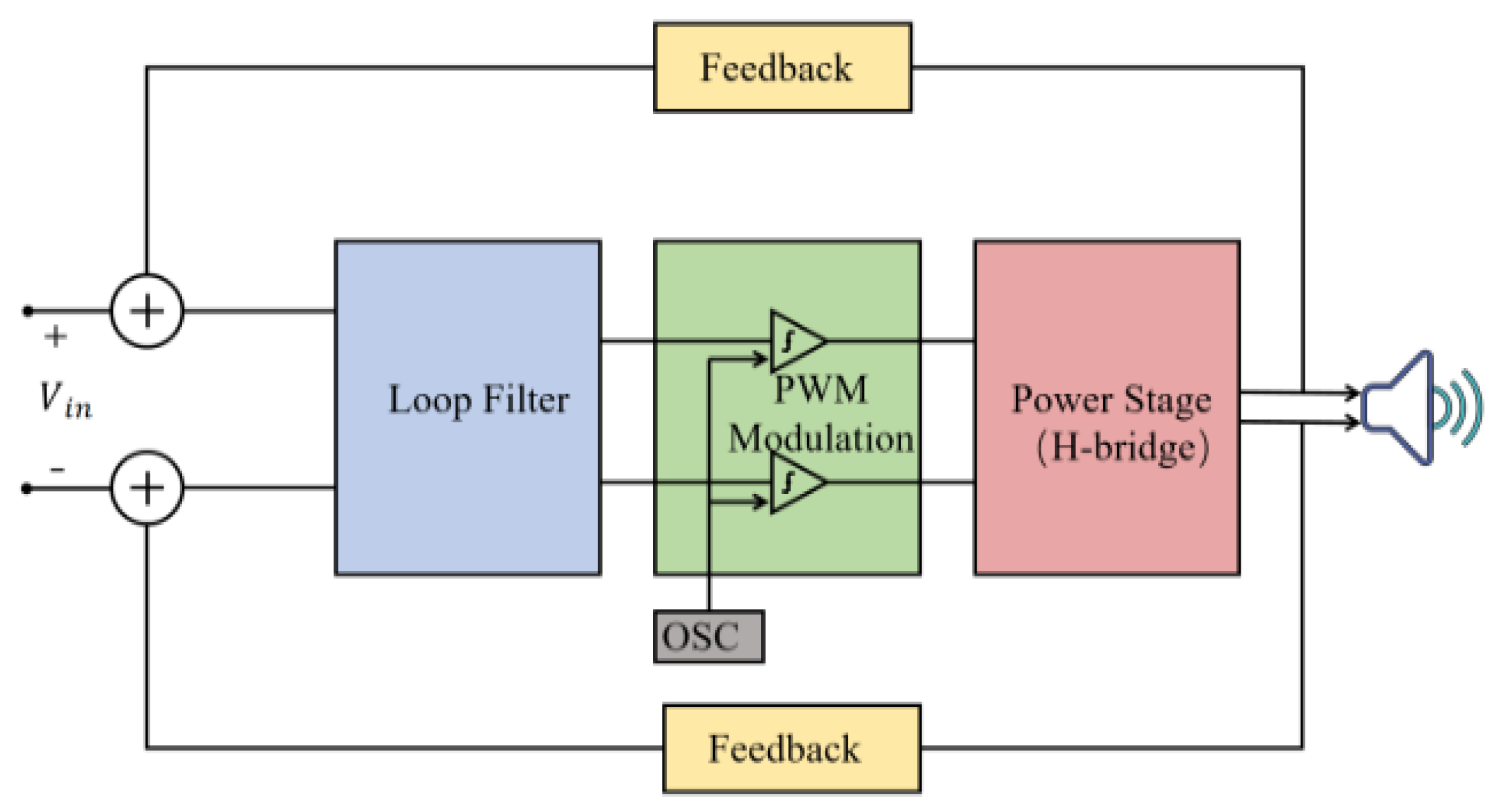
A widespread closed-loop analog Class D amplifier covers integrators, modulators, output stage, low-pass filters, and loudspeakers (
Figure 2). In the first step, integrators and filters provide high loop gain and attenuate unwanted carrier components in the loop. The low-pass filter is always designed between the output model and the loudspeaker to de-crease EMI (electromagnetic interference) and exclude extraordinary frequency energy [
11,
12,
13]. A simple RC network in the negative feedback loop can significantly reduce harmonic distortion and ameliorates the PSRR [
14].
The transistors operating in the saturation or linear region limit the power efficiency of a linear amplifier due to the significant voltage drops that are caused by the large current, resulting in a substantial power loss that greatly influences the efficiency. Class D amplifiers have a unique topology that dissipates less power than the linear amplifiers mentioned above. The output stage works by switching between positive and negative and producing a series of voltage pulses, while the output transistor has no current without switching and low V
DS when managing the current, thus forming smaller I
DS [
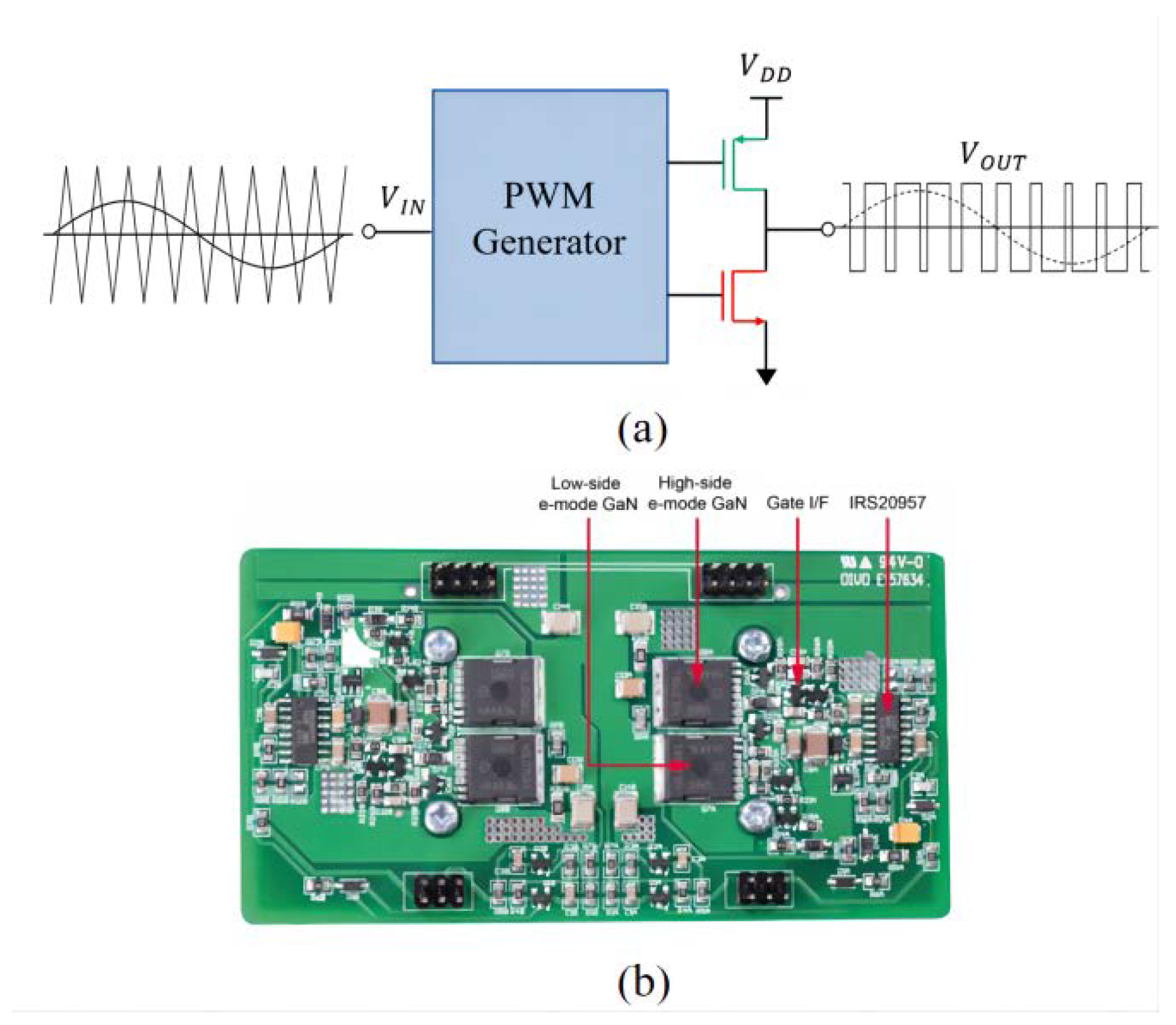
13]. The topologies of Class D amplifiers are shown in
Figure 3a; analog audio signals are sampled and pulse-width-modulated signals are generated. These signals are used to drive the output switches. The signals generated by the output stage will be filtered by the filtering circuit or the speaker itself and converted into sound signals.
The Class D amplifier’s performance is outstanding at the medium and high-power output. However, because of the losses in power devices, the efficiency is lowest if the power output is inadequate. Some Class D amplifiers operate in two modes to overcome this challenge. The multistage technique limits the output voltage to which the power device can switch if playing low-volume audio. Once the output volume reaches a set threshold, the output voltage rail of the switch is increased to provide a complete voltage swing. Zero voltage switching (ZVS) technology can be used at a low output and hard switching at high-power levels to help reduce the impact of switching losses [
16,
17].
The output stage is the foundation of the power amplifier.
Figure 4 shows an essential CMOS (complementary metal oxide semiconductor) linear switch output stage, which amplifies the signal current into a large current that can drive loudspeakers by adding the energy of DC to the slight wind to the input through the triode. In traditional transistor amplifiers, the output stage contains a transistor that provides a continuous instantaneous output current. Many audio linear amplifiers contain Class A, Class AB, and Class B amplifiers. Compared to digital amplifiers and Class D amplifiers, the power consumption is significant even in the most efficient linear region. This diversity makes Class D amplifiers hugely beneficial in many applications. Lower power consumption generates less heat, saves space and cost, and extends the service time of mobile systems.
3. Modulation for Class D Amplifier
A modulator in the Class D amplifier is a circuit that converts an audio signal form an analog signal to a digital signal, and the topology of the modulator usually affects switching errors, dynamic power effects, and distortion. The Class D amplifier is categorized as four ordinary models based on several varying modulation programs, which are pulse-width modulation (PWM), pulse-density modulation (PDM), Δ-Σ modulation, and self-oscillating [
18]. Although there are many design differences, the types of Class D amplifier can still be classified according to the modulation type.
3.1. Pulse-Density Modulation and Pulse-Width Modulation
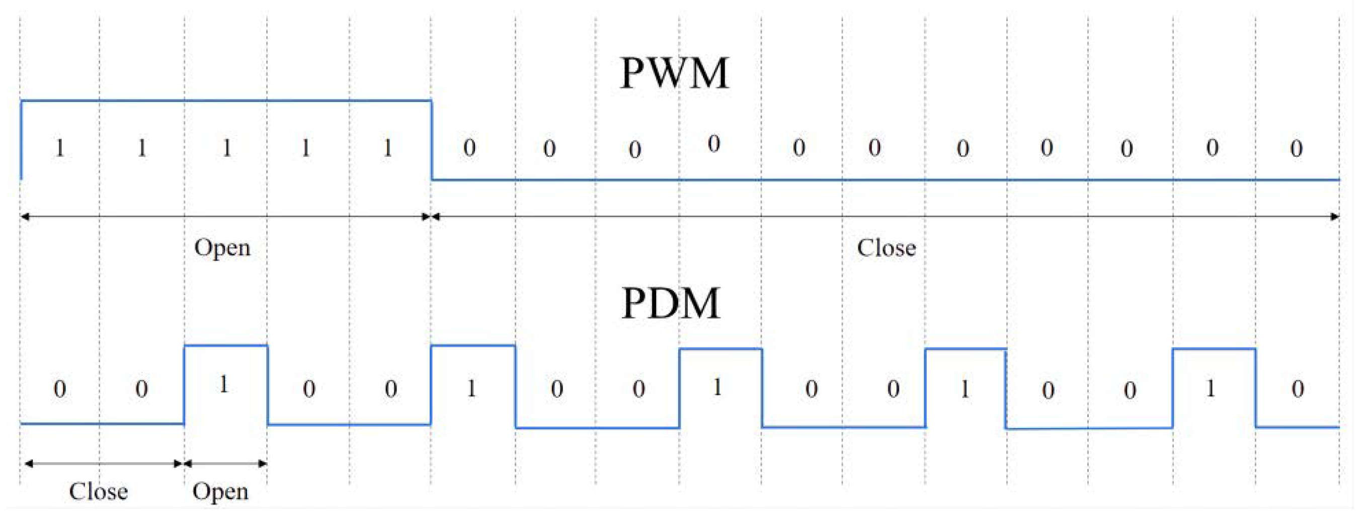
The most common type D modulation scheme is PDM or PWM. The PDM method utilizes the binary number 0,1 to represent an analog signal. In PDM signals, the analog signal’s amplitude is split into the region’s density corresponding to the output pulse. The PWM wave has a particular case of the fixed conversion frequency of the PDM wave. The average value of the two waveforms is 50%; the difference is that PDM wave-switching is more frequent. For signal levels of 100% and 0, the output of both methods is the same.
Figure 5 shows the comparison of PDM and PWM waveforms; “1” is the pulse signal and the state of the output stage “ON” [
19].
If the voltage is expressed in the same resolution, the average clock rate for both PDM and PWM is the same; however, the frequency of PDM signal switching is higher because the signal would rotate between “ON” and “OFF” every other cycle. The PDM modulator output switches at an ordinary rate that is slightly lower than
(sample frequency). For the PWM output, it switches at the rate of
(crystal oscillator frequency) [
20].
In contrast, PWM has a lower switching rate and less switching device movement in any given period. In general, the of PDM is in the order of 100 MHz, while the frequency of the PWM modulator is on the level of kilohertz. Thus, the use of PWM in Class D amplifiers helps to reduce switching errors, while increasing the service life of the switching device. In addition, because the high-level and low-level distribution of PDM is uniform, the proportion of high-frequency components is more significant, so a tiny resistor and capacitor (wide bandwidth low pass filter) can filter enough AC components. However, the PWM has higher requirements for a peripheral filter.
The influences of PWM modulation and PDM modulation on THD (total harmonic distortion) are analyzed in [
21] and verified experimentally at different frequencies. The results show that with the increased switching frequency, the THD value of PDM modulation decreases, and conversely, the THD value of PWM modulation increases. The results validate the most significant disadvantage of PWM modulation: its inherent nonlinearity resulting in distortion.
3.1.1. SHEPWM and SPWM Modulation
In the history of electronic power development, PWM has appeared in a variety of derivative technologies. SHEPWM and SPWM are two of the standard technologies that can be used in Class D amplifiers:
SHEPWM:
The selective harmonic elimination pulse width modulation (SHEPWM) technique is introduced in [
22,
23]. In [
24], a Class D amplifier based on SHEPWM is designed, which uses a GaN power transistor and achieves 0.48% total THD. The SHEPWM switching angles are first pre-calculated and stored in a memory. This differs with the PWM signal, which uses a reference signal and comparator to generate a signal.
Compared to conventional PWM, SHEPWM generates pulse signals according to the switching angle calculated by language, thus, eliminating some harmonics.
Figure 6 below shows a quarter-wave symmetrical three-level PWM with N switching angles per quarter cycle. In this PWM, the DC component and even harmonics are 0, and the odd harmonics are eliminated. Its signal can be described as a Fourier sequence (1):
where
is the angular frequency,
is time,
is the harmonic order, and
is the coefficient of the
order harmonic and is equal to (2):
SPWM:
Sinusoidal pulse width modulation (SPWM) is a modulation technology widely used in motor drive, inverter power supply, and other fields. SPWM can also be used with class D audio amplifiers, for instance, the authors of [
25] designed a Class D amplifier using SPWM; the THD of the Class D amplifier is 0.23%. SPWM wave is a kind of PWM waveform that changes according to sine law. It is a type of PWM technology equivalent to the sine wave effect. The basic principle of SPWM is area equivalence. When a narrow pulse with the same impulse but a different shape is applied to a link with inertia, its effect is the same [
26].
According to the voltage polarity of PWM, SPWM waves can be divided into unipolar and bipolar. in the negative half period of the sine wave, PWM also has only one polarity, but it is the opposite of the positive half period. The bipolar SPWM control circuit is relatively simple compared with the unipolar SPWM mode, and the output voltage of the unipolar SPWM mode is much smaller than the bipolar SPWM mode in the high harmonic component, which is an advantage of the unipolar mode. In general, compared with PWM, PDM is more suitable for high-frequency work and has higher requirements for filters, but the loss of switching devices is higher. All things considered, most amplifiers use PWM.
3.1.2. AD and BD Modulation in PWM
AD and BD modulation are two popular modulation schemes for PWM. For example,
Figure 7 shows two primary working states of bridge H under the AD modulation scheme. The switching device of OUTP and the switching device of OUTN switch states at a 50% duty cycle and opposite polarity. OUTN can be seen as a complement to OUTP. A low-pass (LC) filter with a cutoff frequency lower than the switching frequency should preserve energy for inductive amplifier coils [
27].
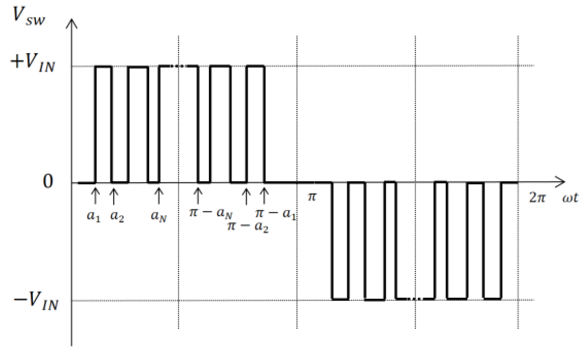
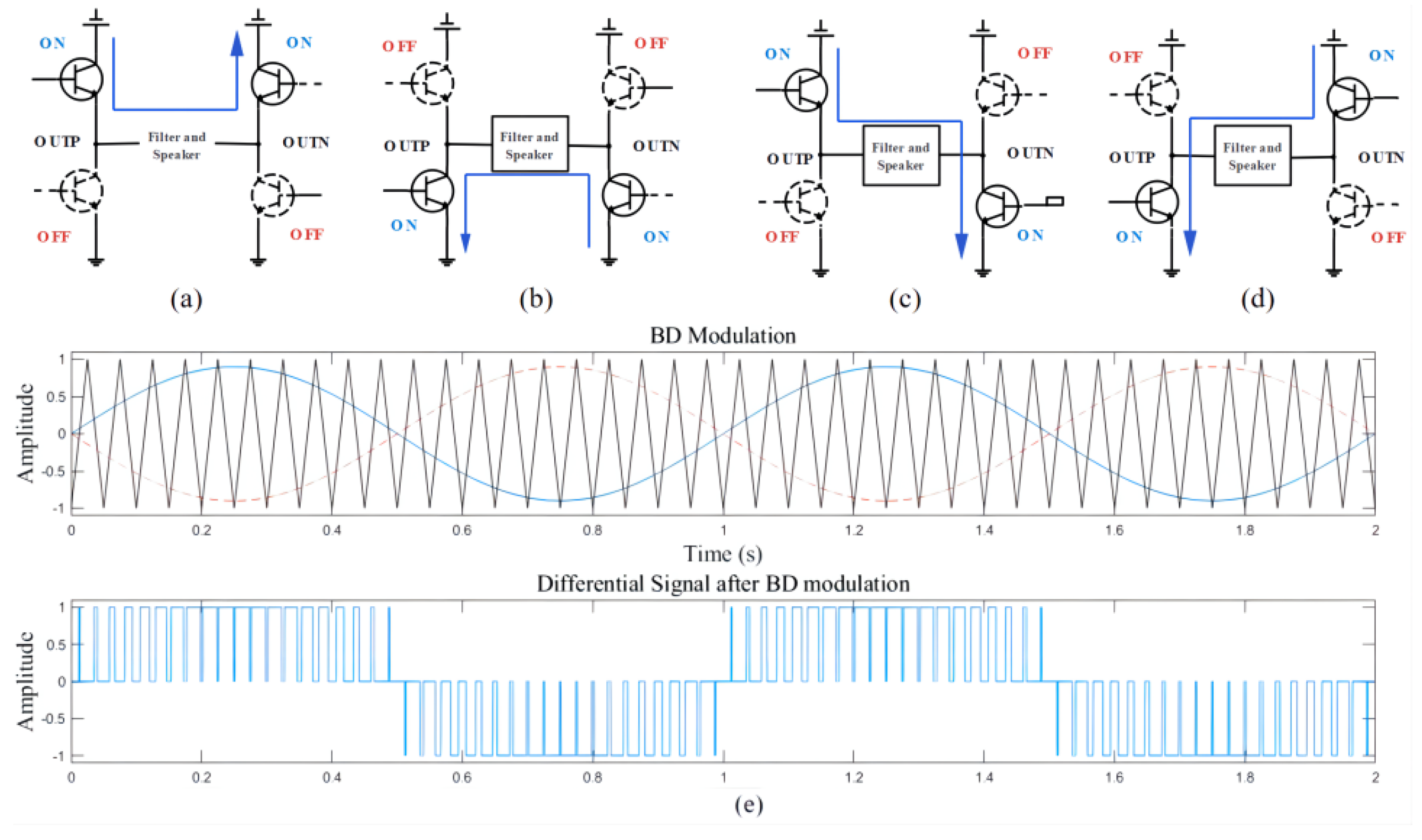
The manipulation of BD modulation is more involved than that of AD modulation. According to the conditions of the input signal, it has four states: modulation processes are shown in
Figure 8a–d, among which the first two states are consistent with AD modulation. Since the current loss is slight at 0 input, the low-pass LC filter is unnecessary.
3.2. Δ-Σ Modulation
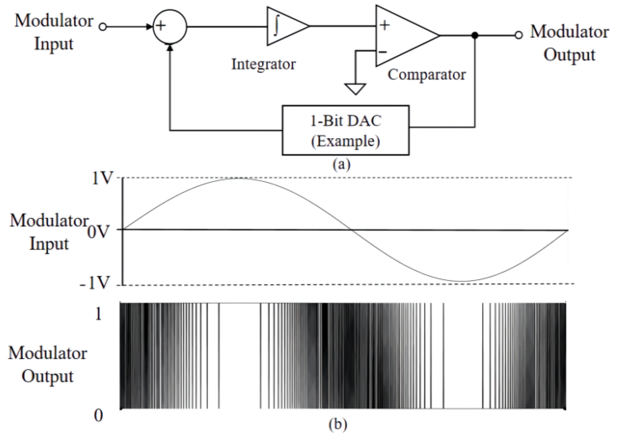
The Delta-Sigma (Δ-Σ) modulation is a modulation method that provides lower output noise and non-linearities to the Class D amplifier.
Figure 9a illustrates a topology of a Δ-Σ modulator, which runs according to the modulator clock, which identifies the sampling interval of the input. The modulation cycle starts by integrating the difference between the input sample and the 1-bit DAC. Each modulator clock pulse produces another modulator output pulse. The resulting output bitstream becomes an alternate representation of the input voltage proportional to the reference voltage.
Figure 9b shows the input sine wave and the resulting modulator output bitstream, assuming a reference voltage of 1 V. As the input approaches 1 V, the 1 s density of the modulator’s bitstream approaches 100%.
The distortion caused by this type of modulation makes the method imperfect for Class D amplifiers. A series of improved designs have been proposed; for example, A class D GaN audio amplifier using Delta-Sigma modulation is introduced in [
28], and the improvement is noticeable. And [
29,
30] presented a low-power class-D audio amplifier using a first-order sigma-delta modulator as a PDM modulator; this design can effectively improve efficiency.
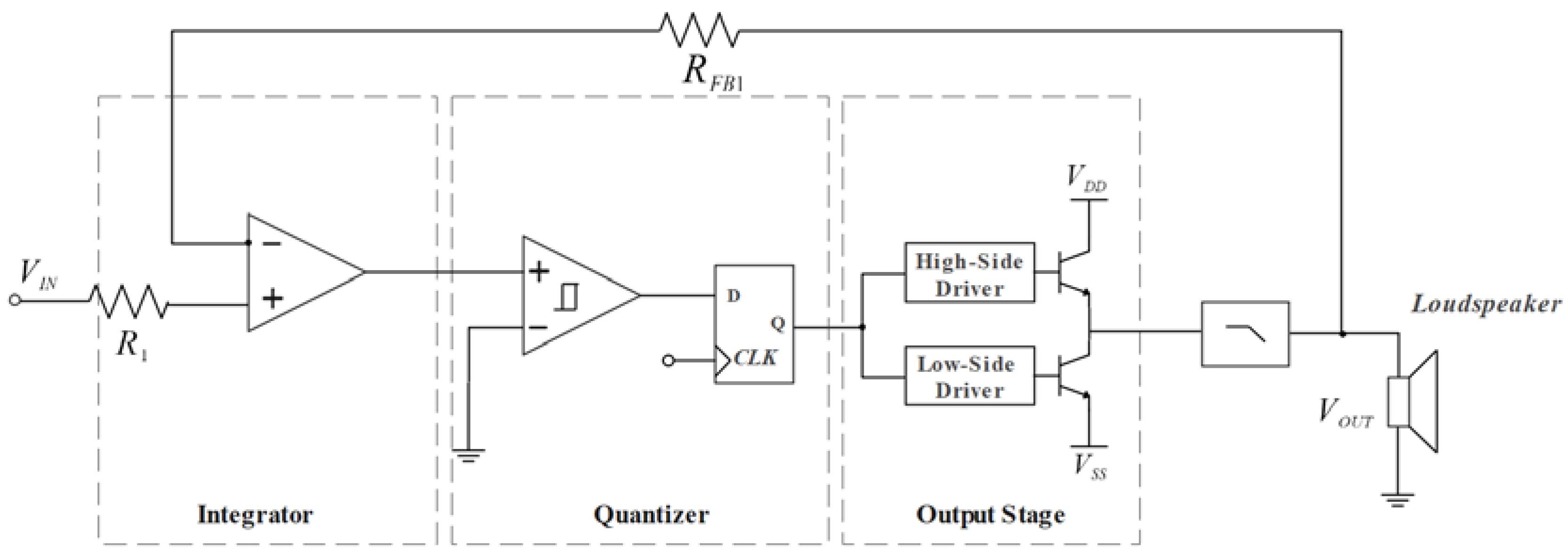
Depending on the quantizer design, Delta-Sigma Class D amplifiers can be classified as synchronous or asynchronous.
Figure 10 shows a synchronous δ Sigma Class D amplifier with a quantizer of a comparator and a Class D flip-flop with a fixed clock frequency. Higher order modulators and higher sampling frequencies can significantly reduce nonlinearity, especially in-band quantization noise, and lead to complex hardware and higher costs.
An asynchronous Class D amplifier with a hysteresis comparator as a quantizer is shown in
Figure 11. Its quantization error is zero because the switch depends on input rather than a fixed clock, making the switch continuous [
31]. The disadvantages of asynchronous Delta-Sigma Class D amplifiers are the variability of the switching frequency and the difficulty of multi-channel design coupling on a single IC.
3.3. Self-Oscillating
The operation of a self-oscillating Class D amplifier (
Figure 12) can be viewed as a “high-power” Sigma-Delta converter, which is not PWM based, and the power-stage amplifies a PDM STREAM. The self-oscillating Class D is not founded on an external clock and does not use any flip-flop behind the comparator (compared to a classical Sigma-Delta) [
32]. The frequency of the self-oscillating Class D is influenced by the power supply voltage, integrator behavior, and propagation delays of the comparator and the power-stage; practically, the designer sets the “idle” frequency by adjusting the integrator circuit.
Paper [
33] clearly illustrates the advantages and disadvantages: the first advantage of self-oscillation is eliminating the need for a low-jitter clock source, which is required for high-performance analog and digital input fixed-frequency amplifiers. Switching frequency is subsequently set by an oscillation condition and varies nonlinearly as a function of the input signal. The one-cycle control topology is notable for considerable switching frequency variation [
34]. In addition, since the low-pass filter precedes the feedback, the low-pass filter of the feedback loop can suppress the nonlinearity. Disadvantages of the self-oscillating feature include the intermodulation products that are generated when using multiple amplifiers in a system. Moreover, a large-signal analysis only becomes feasible with simulation, as the small-signal approximations typically only hold for modulation indices of D « 1 [
35,
36].
There are two specifications of the comparator that should be considered. The first important specification is the input-to-output voltage amplitude range. These values determine the amplitude of the square wave produced by the comparator. If the comparator cannot achieve the full rail output signal, the amplitude of the square wave will be limited.
The second specification is the propagation delay. This is the delay for the signal to pass through the internal circuit of the comparator. When signal A exceeds signal B, the comparator produces an output, but the output does not change immediately. The amplifier circuit will not be able to function correctly if the comparator has too large of a propagation delay.
4. The Design of Class D Amplifier
Audio amplifiers seek high power efficiency, superior anti-noise performance, and high audio signal fidelity. However, high efficiency and low distortion are contradictory and cannot exist in the same design. Therefore, the designer needs to determine the basic modulation scheme based on the different requirements of the Class D amplifier, such as maximum power. A well-designed Class D amplifier requires consideration of the appropriate modulation strategy and the topology of the output, the creation of the output filter, and how to deal with EMI problems and power supply rejection.
4.1. Output Stage: Half-Bridge vs. Full Bridge
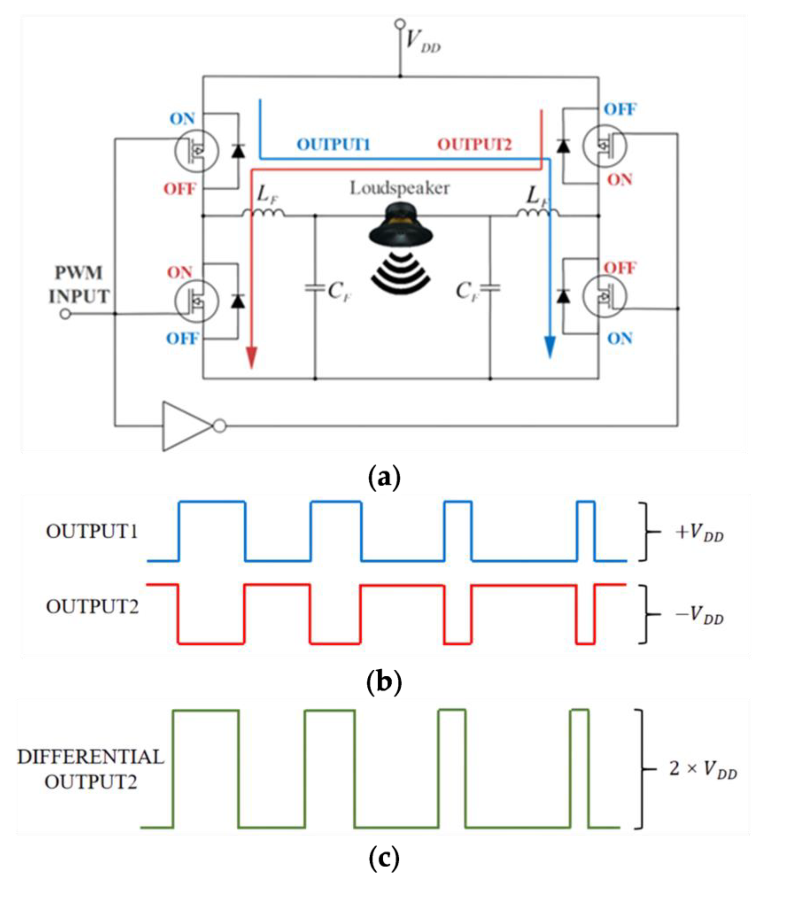
Bridge-tied load (BTL) is often referred to as the full-bridge output stage, and it uses two half-bridge steps to drive the load differential (two output poles), which consists of four switching devices. As shown in
Figure 13a,b, the full-bridge structure operates by alternating the conduction path through the load. In
Figure 13c, the mutually matched output waveform forms a differential PWM signal across the load, which results in an additional LC filter circuit that must be included in the design to prevent hf signal loss in the load [
37].
The main advantages of full-bridge Class D amplifiers over half-bridge structures are:
1. DC-blocking capacitors are not needed when operating with a single power supply because the DC current flowing at its output end is different from the of the half-bridge structure, which is 0.
2. The load is differential driven; a full-bridge Class D amplifier can achieve twice the output signal amplitude of a half-bridge amplifier at the same supply voltage. It also means more than four times the theoretical maximum power output [
38].
The disadvantage of full-bridge Class D amplifiers is that the number of switching devices required is twice that of the half-bridge topology, resulting in more conduction and switching losses. This loss is only shown in high-output amplifier applications because of the higher output current and supply voltage. Therefore, the half-bridge structure is usually applied to high-power amplifiers. While most high-power full-bridge amplifiers are 80–88% efficient at 8Ω loads, the half-bridge MAX9742 is 92% [
39].
4.2. Output Filter Design
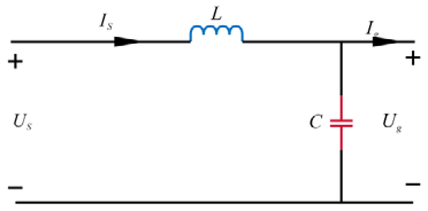
4.2.1. LC Design
A well-designed LC filter can save cost and board space while having a valuable filtering function. Second-order low-pass designs (Butterworth) are popular LC filter designs in Class D amplifiers due to the relatively stable passband frequency response and low hardware requirement [
40,
41]. The topological structure of the LC filter is shown in
Figure 14 below. It can be found that filter inductance and filter capacitance are the two most important elements, and their selection and design are crucial.
The inductance design depended on the DC resistance and rated peak current specifications. The rated current of the selected core should be higher than the maximum expected current of the amplifier. The reason is that the inductor will short circuit if the rated current of the inductor is not enough to service the device’s output current. This will expose the device or speaker to significant current damage. The relationship between the efficiency of the system and the DC resistance of the inductor is (3) [
40].
refers to the loudspeaker resistance, is the output driver transistor conduction resistance, and is the resistance of the inductor.
The choice of capacitance is as essential as the inductance. The most critical parameter in evaluating high-frequency chip capacitors is a dimensionless value
Q (quality factor), which is related to the associated equivalent series resistance (
ESR); the relationship of these elements is shown in (4). The
ESR measures the loss of a capacitor at a given frequency, and its value should be as small as possible, close to 0 Ω. The current flowing through the capacitor will advance the voltage at both ends by exactly 90° at all frequencies. However, in practice, capacitors always exhibit some degree of
ESR [
42].
Since both reactance and resistance vary with frequency change, Q is significantly influenced by frequency. The capacitance reactance will fluctuate considerably with the frequency change or capacitance value; hence, Q will dramatically change.
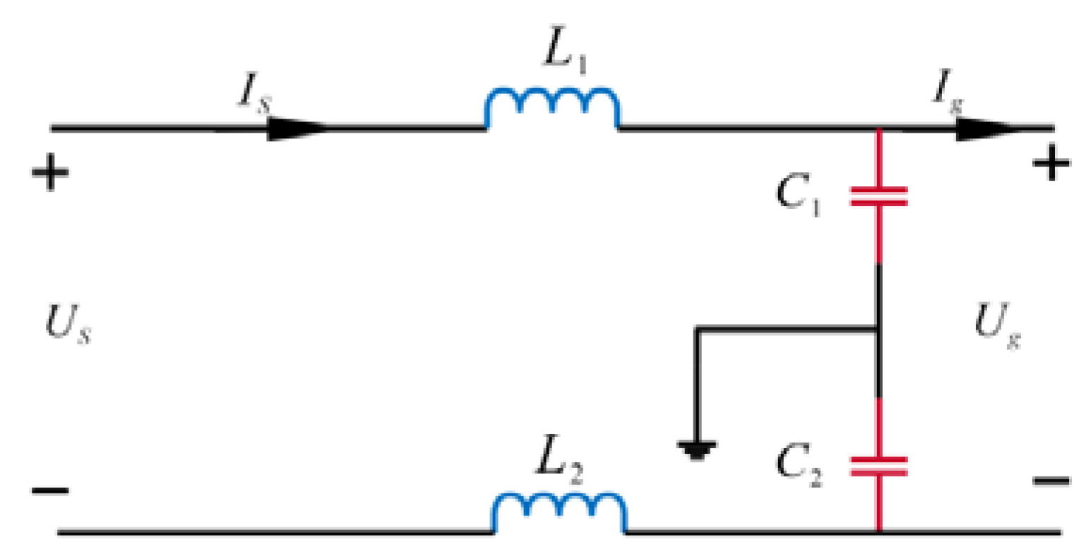
4.2.2. Common-Mode Filters
The common-mode filter refers to the LC filter, which grounds the original capacitor end. Its topological structure is shown in
Figure 15, which consists of two inductors and two grounded capacitors. Compared with the LC filter, the EMI performance of the common-mode filter is greatly improved, and it can effectively filter high-frequency models. Since the two inductors are effectively in a series between MOSFETs, replacing the original LC filter design with two inductors can be considered. For example, a filter design requiring 10 μH inductors can be replaced with two 5 μH inductors in a series. An additional benefit is that common-mode filters are guaranteed to perform well without connected loudspeaker loads, since the response, unlike that of a differential mode filter, mainly derives from load-damped loudspeakers. However, the common-mode filter has the following disadvantages: 1. It has an underdamped common-mode response, which may cause unnecessary ringing on the speaker load. 2. The ripple current will increase as the number of inductors and capacitors increases [
43].
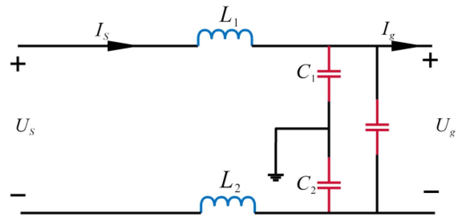
4.2.3. Topology of Common-Mode Filters
The structure that combines a common-mode filter and a differential filter is named a hybrid filter. The topology is shown in
Figure 16, which can be considered a capacitor in parallel between the common-mode filter and the speaker load. Such a design can reduce the cost of the filter and provide the benefits of a common-mode filter. A well-designed hybrid filter costs slightly more than an equally effective differential amplifier and provides common-mode attenuation and damping without connecting loads. As the value of the differential filter can be designed to be much higher than the value of the common-mode capacitor, the capacitor can be used for the cheaper metal film capacitor’s differential capacitance and the common-mode capacitance of the more inexpensive multilayer ceramic capacitor. However, the advantages of the hybrid filter may be more evident in some cases: 1. The differential mode damping of the hybrid filter under no-load conditions is reduced because current will pass through the more considerable differential mode resistance, which may fail to protect the amplifier under no-load conditions. 2. The differential attenuation of the hybrid amplifier is the same as that of the common-mode filter. Nevertheless, the common-mode capacitance of the hybrid filter is smaller than that of the common-mode filter, therefore, the common-mode attenuation is not as sound as that of the common-mode filter, and the attenuation at the switching frequency and harmonics is also lower. 3. Hybrid filters typically have higher distortion due to less effective ceramic capacitors in pursuit of cost reduction [
44,
45].
4.2.4. Filterless Amplifiers
The filterless design of Class D amplifiers is becoming a popular technology [
46]. The superiority of the filterless operation of Class D amplifiers includes saving the space and cost of filters and superior IMD performance. Intermodulation distortion (IMD) is caused by non-linearities in the system, and the computational formula of IMD is as shown in (5) [
47].
In [
48], the IMD is studied using a double Fourier analysis model, and the linearity of a closed-loop filterless Class D amplifier is further understood. The results show that the performance of IMD is better than that of a second-order closed-loop Class D amplifier without the filter. A higher loop gain in classical linear amplifier design theory will improve linearity and reduce IMD. Nevertheless, Class D closed-loop amplifier behavior is opposite to classical linear amplifier design regulation. Another detail that can be observed is the in-band loop-gain increases; the IMD of the second-order amplifier improves simultaneously with the clock frequency loop gain. In other words, the amplifier’s IMD capability deteriorates as the out-of-band attenuation decreases.
Loop filters distort the amplifier’s output signal. In traditional PWM closed-loop Class D amplifiers, in-band gain and stopband damping are inversely correlated. That is, increasing in-band gain leads to a decrease in stopband damping. The loop filter must afford high in-band gain and high stopband attenuation to filter the PWM clock frequency, in order to filter the track-to-track signal. A compromise design was needed to resolve the paradox, requiring prominent in-band gain to accomplish high PSRR, THD, and high stopband attenuation to exclude high-frequency rail-to-rail feedback signals [
49,
50]. A characteristic filterless amplifier is shown in
Figure 17. The analog input module is combined with a negative feedback circuit in the output stage and fed to a low pass filter (loop filter). The filter provides superior in-band gain but still attempts to attenuate signals at higher frequencies [
51].
4.3. Taming EMI
The design and selection of high-frequency components output by Class D amplifiers are worthy of careful consideration. As high-frequency components can generate significant electromagnetic interference and disrupt the operation of other devices, EMI noise is entirely unpredictable to surround devices and circuits, affecting several RF systems in mobile phones, such as call, radio, and other functions.
In paper [
51], it was mentioned that the energy of electromagnetic interference (EMI) depends mainly on the time and magnitude of the change. It spreads in two ways: Electromagnetic interference is divided into conducted electromagnetic interference and radiation electromagnetic interference. With the electromagnetic interference frequency of 30 MHz as the boundary, electromagnetic interference smaller than 30 MHz mainly generates noise in electronic equipment through conduction. When the frequency is higher than 30 MHz, electromagnetic interference mainly produces radiation.
The common EMI standards are FCC (Federal Communications Commission) and CISPR (Special International Committee on Radio Interference).
There are two main methods, which are shown in [
39], to reduce EMI for Class D power amplifiers:
1. The power amplifier adopts the spread spectrum technology for the sampling frequency. Consequently, the EMI interference spectrum caused by sampling frequency is relatively average to reduce EMI.
2. Controlling the opening and closing time of the output tube controls the EMI interference on edge. It is generally considered that the second point is the main factor affecting the EMI of the Class D power amplifier.
To reduce the EMI of the interference signal is to change the interference frequency. Shortening the speaker line of the Class D power amplifier can reduce the transmitting efficiency of the antenna, which reduces the intensity of interference radiation waves. The method uses the LC filter to remove the audio signal from the switching signal of the Class D power amplifier and transmit it to the speaker through the speaker line. As the length of the Class D power amplifier’s horn line is relatively short in the application of portable electronic products, magnetic beads can be used to filter some high-order harmonics without the use of the LC filter to achieve the effect. The specific operations for reduction are as follows:
1. Using the frequency hopping method can also effectively avoid interference. Suppose the receiver is disturbed by the high-frequency switching signal of the Class D power amplifier while receiving one frequency. In that case, the high-frequency switching frequency of the Class D power amplifier can jump to another frequency. Since the audio content of the Class D power amplifier is independent of its carrier or switching frequency, this method does not affect the audio signal content. If the switching frequency is not in the receiver’s bandpass filter region, the receiver can effectively suppress the interference signal [
52].
2. Another solution to EMI is to use metal shell shielding to attenuate the interference energy of harmonic radiation to normalize FM reception. However, this shielding method is not applicable if the FM receiver is combined with a Class D power amplifier.
4.4. Power Supply Rejection
Power supply rejection refers to the power supply’s input and output as independent signal supplies. The amplitude ratio of the input signal to the output signal is PSRR, which is usually expressed as an exponential, and the unit is “dB”. The power supply rejection is due to the output stage low-pass filter only suppressing the high-frequency noise; it is difficult to restrain the noise from the audio frequency of the power supply. The study of [
50] discussed the influence of power supply noise on single-ended and differential switching output stages. If the distortion and the power supply problem are severe, the PSRR will be less than 10 dB, and the THD will be less than 0.1%.
Many solutions to the PSRR problem exist. The LC filter with high loop gain is one of the solutions to improve PSRR and attenuate distortion. The nonlinearity of the LC filter can be reduced by designing speaker impedance in the feedback circuit. However, in using integrated circuits to achieve the above design, the analog circuit to capture the time error and the feedback circuit design will significantly increase the complexity of the chip, resulting in a significant increase in cost. As a result, some manufacturers prefer to replace analog circuits with digital open-loop regulators; however, distortion problems persist. This open-loop Class D amplifier is usually used in the domain where sound quality is low [
53].
5. GaN-Based Class D Amplifier
In the case of mobile devices with limited battery capacity, working efficiency is a crucial design metric. Although the Class D amplifier has a power consumption advantage over other amplifiers, it still suffers from low fidelity, mainly due to switching distortion.
The processors of Class D amplifiers produce small high-frequency pulse width modulation (PWM) signals that represent the auditory signal. The power transistor converts small signals into significant signals in half-bridge or full-bridge configurations and drives the speaker through a filter. Increasing the adoption frequency and the output stage switching frequency can significantly increase the sound because each pulse is a square wave. Power is wasted by switching losses and conduction losses in each switching cycle, thus, balancing sound quality, operating frequency, and power consumption [
54]. Switching loss is another factor that requires proper consideration. Thus, the essential component of the Class D amplifier is the switching device, whose quality directly determines the strength of each indicator of the amplifier (examples are SNR, THD, and TID (transient intermodulation distortion)). Class D amplifiers must employ integrated feedback circuits to compensate for poor open-loop performance, in order to complete the distortion performance goals (THD + N, TIM, and IM) that are required for high-quality sound.
The source of this distortion is the power MOSFETs based on Si. Thus, the primary goal of a progressive Class D amplifier is to improve its switching structure. An excellent choice to for the MOSFET or IGBT is the GaN device or SiC device [
55].
5.1. Advantages of GaN Power Device
After decades of intensive development, Si-based power devices are approaching their material limits in terms of performance. Power devices based on wide-bandgap semiconductors with a higher critical breakdown field are desired to enhance the device performance further, and thus, the power conversion efficiency. Research on power devices has been ongoing for many years. The advent of wide bandgap (WBG) semiconductors based on gallium nitride (GaN) or silicon carbide (SiC) enables Class-D amplifiers to achieve outstanding performance regarding distortion and bandwidth [
56]. According to [
57], GaN devices have the advantage of operating at higher voltages and lower leakage currents than Si devices. Compared with the first-generation Si and the second-generation GaAs, the third generation GaN and SiC devices have small on-state resistance, fast switching speed, and high voltage performance. The GaN device has a vacuum saturation rate of 2.8 times that of Si devices, making its on-resistance and conduction losses much lower than Si devices. The common junction capacitance of GaN devices enables its switching frequency up to the Mhz level. The bandgap of the GaN device is much smaller than that of the silicon device, which causes its critical breakdown electric field to be as high as 3.3 MV/cm; therefore, it has a higher voltage capacity. The comparison of parameters between the GaN device and Si device is shown in
Table 1. The larger bandgap width and the insulating damaged electric field reduce the device’s conduction resistance and improve its overall performance. The resulting high-electron saturation rate and high carrier mobility enable the device to work at high speeds [
58,
59]. Moreover, GaN transistors have more applications due to showing higher switching dynamics and incorporating fewer parasitics in their packages. The experiments in [
60] demonstrated that GaN devices can lead to a higher power and lower THD in Class D amplifiers. GaN devices play an essential role in many fields, especially in the improvement of power efficiency. It is feasible that these devices could also initiate a revolution in the field of audio power amplifiers [
61,
62].
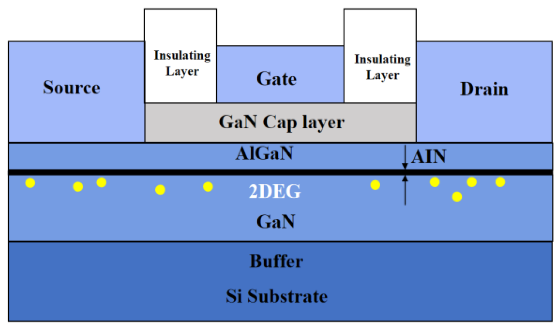
As shown in
Figure 18, GaN HEMT transistors are the same as Si MOSFET terminals, with a gate, drain, and source [
63]. This also indicates that GaN HEMT has similar functions to Si MOSFET and can substitute for power devices in Class D amplifiers. They achieve meager resistance with the help of a two-dimensional electron gas (2DEG) between the gate and the source and can be effectively short-circuited due to the availability of an electronic pool [
64]. The p-Gan gate will stop conduction while there is no gate bias (VGS = 0 V). Gan HEMT is a bidirectional device, unlike silicon devices. Therefore, a reverse current may occur if the drain voltage is permitted to fall below the source voltage. Gan HEMT transistors have the advantage of a clean switching waveform—mainly, the absence of the bulk diodes commonly found in Si MOSFET, which is responsible for much of the switching noise associated with the PN junction [
65]. If the amplifier works in zero-voltage switching mode, the switching loss and the power loss can be effectively eliminated because the output transformer is realized by inductance current conversion. At present, most GaN power devices have a planar structure like
Figure 18. If the substrate in this structure has minor lattice and thermal mismatch with GaN material, the uneven phase denotative growth of GaN can be implemented. GaN power devices comprising Si material for the substrate have mature technology and low cost, which is the optimal solution of Class D amplifier power devices [
66,
67].
5.2. Analysis of GaN Class D Amplifier
Table 2 provides several typical power amplifiers using GaN devices, which are characterized by high power efficiency and low THD. The power density of GaN semiconductors is more than ten times that of the latterly diffused metal oxide semiconductor (LDMOS) transistors used in conventional power amplifiers, with higher power density and efficiency. If we use GaN to make IP, we can obtain more power for the same size and a smaller size for the same power. For high power, efficient audio power amplifiers, GaN HEMT using power loss, power density, and response speed are better choices. Compared to traditional Si MOSFETs, GaN HEMTs have a higher rate, cost of arable land, and better performance and thermal efficiency.
Given the critical indicators of Class D amplifiers, GaN devices have corresponding advantages or disadvantages. The following paper cites the current research results for analysis:
5.2.1. Power Efficiency and Distortion
More than one article has mentioned the advantages of GaN devices over MOSFET and IGBT, especially in [
74]. Further, in [
75], the effect of the 60 V GaN device and Si device Class D audio amplifier is compared, and the conclusion is drawn that the power density of the GaN power device is much higher than the Si device. In [
71] is described the effect of GaN transistors in conventional power amplifiers, achieving over 30% power savings and higher power density and efficiency. Compared with traditional Si MOSFET, GaN FET has higher speed, lower cost, and thermal efficiency. Although the Class D amplifier designed in [
72] has an efficiency of only 85.8%, this is because the rated circuit of the transistor used in this design is much larger than what the circuit needs, and higher power can be obtained with a more suitable FET.
The power level of Class D amplifiers aims to achieve accurate large-signal replication from small signal sources while reducing energy loss. Better switching properties of the GaN-based FETs produce waveforms that are closer to the desired ideal waveforms than can be achieved by silicon Mofettes. This is an essential benefit of GaN devices, which can switch up to 1000 times faster than silicon FETs. GaN systems’ white paper quantifies this superb audio quality, showing that GaN-based Class D amplifiers can produce total harmonic distortion (THD) as low as 0.004%, compared to 0.015% for silicon products [
77,
78]. A PDM 25 W Class D amplifier with GaN and Si devices as output stage is tested and compared in [
79]. The test results show that when the output power is less than 20 W, the power amplifier’s distortion based on the GaN device is 0.15% lower than that of the power amplifier based on the Si device, and the power efficiency is 15% higher. In addition, at lower switching frequencies (360 kHz), the two output stages’ distortion performance and power efficiency are similar. At higher switching frequencies (>1.1 Mhz), the GaN output stage has considerable advantages [
80].
In addition, in zero-voltage switching mode, the output is changed by inductive current commutation. Therefore, any switching loss in the switching device and the resulting power loss can be moved. However, to avoid shoot-through between the two devices, a small blanking delay must be added to ensure that the off-state of the switching period is maintained until the on-state of the next switching period is entered. the output waveform is different from the waveform expected by the PWM output, resulting in audio signal distortion. The blank delay time depends on the output capacitance Coss of the power device used. Compared to Si MOSFETs, GaN transistors have significantly lower Coss, which means that blanking delay time can be minimized, thereby minimizing distortion.
Therefore, power density, power efficiency, and switching frequency advantages indicate that GaN devices will enable a smaller circuit footprint, lower thermal radiation, and long service life, which bridges the direct contradiction between power efficiency and sound quality. However, cost and the lack of a dedicated Class D amplifier integrated circuit are disadvantages of GaN devices.
5.2.2. Thermal Conductivity
Heating is one of the main problems of GaN devices due to the high-power densities. Due to the high conductivity of the SiC, it is a common method of growing GaN on SiC substrate to limit the temperatures of GaN HEMT to no higher than the maximum temperature [
3]. Some variations reported across the literature, such as the GaN output stage, introduce performance reduction after high temperature, which is an essential disadvantage of GaN devices [
80,
81]. However, the growth of GaN involves particular transition layers typically involving alloys of GaN and AlN, which have inferior thermal conductivity because of disorder-induced phonon scattering. In some cases, the performance limiting factor of GaN might be its thermal conductivity as opposed to its electronic properties. Thus, the heat dissipation of audio systems using GaN devices will be one of the following research focuses. The TMT (Thermal Management Technologies) program introduces several cooling technologies of heat management in semiconductors, such as attached cooling and embedded cooling technologies [
82,
83,
84]. The junction temperature of the GaN devices is usually generated at the drain side of the gate, and for this reason, the thermal management solutions should focus on the heat area.
In [
85,
86], near-junction embedded microfluidic cooling methods are recommended, which have an excellent effect. This technology is already suitable to replace traditional passive remote cooling techniques.
In [
86], the feasibility of using diamond as a substrate for GaN devices was investigated. In [
87], diamond microfluidics-based intrachip cooling was used to influence the heat outflow from a model with low thermal conductivity. In addition, the cooling effects of active and passive cooling techniques on GaN devices with SiC as substrate and diamond as substrate were studied in [
88].
5.2.3. EMI
The high switching speed of GaN devices will deteriorate the EMI in the amplifier. There have been many articles studying the EMI produced by GaN in converters and its effects, for example [
89,
90,
91,
92,
93]:
Compared with the Si MOSFET, the full-speed (more than 100 MHz) GaN device increases the EMI to 10 dB. Some EMI reduction schemes are proposed, such as selecting the original [
94], modifying the topology of the converter circuit [
90], or improving the filter [
93]. The research on audio amplifiers is still insufficient at present:
In [
94], audio amplifiers were built using the SPICE models of fundamental drivers and GaN transistors, which allow an accurate GaN power stage. Moreover, the paper hypothesizes that the model and the object may not be accurate; this error occurs in the low-frequency band. The reason is that the simulation model produces significant spikes of drain currents at the beginning of transistors turning on. In [
95], a simple method for the conductive EMI modeling of integrated Class D amplifiers is shown. However, the work does not consider the control circuits of GaN transistors.
The influence of the transistor’s current spikes on the EMI level grows with increasing frequency. Higher switching frequencies flatten the interference spectrum in the entire measurement band for both modulated signals and signals with no modulation. The influence of stray parameters also increases.
6. Discussion
The Class D amplifier has lower efficiency distortion and a better frequency–response curve. More importantly, compared with Class A, Class B, and Class AB, it has higher efficiency and less distortion, and the power amplifier transistor consumes less power and has better heat dissipation. Fewer peripheral components have merits. An excellent audio system needs to achieve the best sound at the lowest cost and high-power efficiency. The low power consumption of Class D amplifiers saves the price (and PCB area) of cooling devices such as fins or fans. Class D integrated circuit amplifiers can be packaged in smaller sizes and at lower costs than analog linear amplifiers. Due to these advantages, the Class D amplifier is widely used in audio systems.
The switch element in the output stage is an essential factor affecting the audio quality of the Class D amplifier. In the past, the development of Class D amplifiers was restricted by the inefficiency of switching devices. It was not until the application of MOSFET that Class D amplifiers were widely used in audio systems. The advantage of Class D amplifiers is simultaneously improved power efficiency and audio and reduced distortion, provided that a better power switching device is available. Class D amplifiers require lower switching voltages and faster and more accurate switching transitions. GaN devices are the new key to the progress of Class D amplifiers. The simulation and experimental results show that GaN-based switching devices have the advantages of small size and high efficiency (increased by nearly 15% [
68] compared with Si MOSFET). In addition, they have lower power loss and higher accuracy under the condition of a high switching frequency. GaN FET and the outstanding switching performance of the integrated chip provide near-ideal waveforms to achieve lower distortion and better sound quality than silicon MOSFETs.
High-performance power devices are necessary to achieve high power efficiency and high fidelity, which require more minor switching losses to increase service life and reduce power losses. The GaN device is a kind of power device which can meet the above requirements, and it compensates for the deficiency of the Si device. GaN-based high electron mobility transistors (HEMT), as typical GaN power devices, possess all the advantages mentioned above and can be used as switching devices in Class D designs, providing higher efficiency and audio quality. Class D audio amplifiers based on high refresh rate switching devices such as GaN HEMT and GaN FET can approach the maximum power efficiency and minimize audible noise due to the smooth switching characteristics. The performance heralds a new era of high-quality, affordable Class D audio amplifiers, enabling Class A-grade quality amplifiers to be introduced into high power audio equipment such as automotive applications.
However, the performance-limiting factor of GaN devices might be the thermal conductivity as opposed to the electronic properties. The literature [
76] reports the poor thermal conductivity due to the specific transition layers typically involving alloys of GaN and AlN. Therefore, to maximize the lifetime and performance of GaN-based amplifier systems, the designers should understand and consider the limitations of the thermal environment.
7. Conclusions
In this paper, the literature on Class D audio amplifiers for efficiency has been reviewed, several modulation methods and designs have been summarized, and the GaN device and the adaptability of GaN devices to Class D amplifiers has been discussed. Audio power amplifiers’ high fidelity and power efficiency are often challenging to achieve in a single amplifier system. However, using GaN devices provides a new possibility of realizing this ideal amplifier. Several studies have demonstrated the advantages of GaN devices in Class D amplifiers, including efficiency and THD. In contrast, the high cost, lack of integrated Class D amplifier circuits that are appropriate for GaN devices, and the influence from heating are the following challenges.
Author Contributions
Conceptualization, S.M. and Y.H.; methodology, H.X.; formal analysis, H.W.; investigation, S.M.; resources, H.X.; data curation, H.W.; writing—original draft preparation, S.M.; writing—review and editing, S.M.; visualization, Y.H.; supervision Y.H.; project administration, H.W. All authors have read and agreed to the published version of the manuscript.
Funding
This research was funded by Royal Society, IEC\NSFC\201119—International Exchanges 2020 Cost Share (NSFC), Royal Society Industry Fellowship (INF\R1\201021), “LF-OCT based Quality Inspection for Power Electronics Module Manufacturing Line”, 1/05/2020~1/05/2024, (£116k) PI.
Conflicts of Interest
The authors declare no conflict of interest.
References
- MarketsandMarkets. Audio Amplifier Market by Channel Type (Mono, Two, Four, Six), Device (Smartphones, Television Sets, Desktops & Laptops, Home Audio Systems, Professional Audio Systems, Automotive Infotainment Systems), End-User Industry, Region—Global Forecast to 2024. 2019. Available online: https://www.marketsandmarkets.com/Market-Reports/audio-amplifier-market-187106441.html (accessed on 25 July 2022).
- Gaalaas, E. Class d audio amplifiers: What, why, and how. Analog. Dialogue 2006, 40, 1–7. [Google Scholar]
- Hamza, K.H.; Nirmal, D. A review of GaN HEMT broadband power amplifiers. AEU-Int. J. Electron. Commun. 2020, 116, 153040. [Google Scholar] [CrossRef]
- Fu, Z.; Anttila, L.; Abdelaziz, M.; Valkama, M.; Wyglinski, A.M. Frequency-Selective Digital Predistortion for Unwanted Emission Reduction. IEEE Trans. Commun. 2015, 63, 254–267. [Google Scholar] [CrossRef]
- Jiang, X. Fundamentals of Audio Class D Amplifier Design: A Review of Schemes and Architectures. IEEE Solid-State Circuits Mag. 2017, 9, 14–25. [Google Scholar] [CrossRef]
- Texas Instruments. TPA2037D1—3.2W Mono Class-D Audio Power Amplifier With 6-dB GAIN and Auto Short-Circuit Recovery; Texas Instruments: Dallas, TX, USA, 2010. [Google Scholar]
- Kwon, S.; Kim, I.; Yi, S.; Kang, S.; Lee, S.; Hwang, T.; Moon, B.; Choi, Y.; Sung, H.; Koh, J. A 0.028% THD+ N, 91% power-efficiency, 3-level PWM Class-D Amplifier with a True Differential Front-End. In Proceedings of the 2012 IEEE International Solid-State Circuits Conference, San Francisco, CA, USA, 19–23 February 2012; pp. 96–98. [Google Scholar]
- Hood, J.L. Simple Class A amplifier: A 10-W design giving subjectively better results than Class B transistor amplifiers. Electron. World 2004, 110, 44–49. [Google Scholar]
- Velasco-Quesada, G.; Roman-Lumbreras, M.; Perez-Delgado, R.; Conesa-Roca, A. Class H Power Amplifier for Power Saving in Fluxgate Current Transducers. IEEE Sens. J. 2016, 16, 2322–2330. [Google Scholar] [CrossRef]
- Yang, F.; Xu, C.; Akin, B. Experimental Evaluation and Analysis of Switching Transient’s Effect on Dynamic on-Resistance in GaN HEMTs. IEEE Trans. Power Electron. 2019, 34, 10121–10135. [Google Scholar] [CrossRef]
- Takagishi, H. Class D Audio Amplifier. U.S. Patent US6489841B2, 3 December 2002. [Google Scholar]
- Kim, J.; Roblin, P.; Chaillot, D.; Xie, Z. A Generalized Architecture for the Frequency- Selective Digital Predistortion Linearization Technique. IEEE Trans. Microw. Theory Tech. 2013, 61, 596–605. [Google Scholar] [CrossRef]
- Kang, Y.; Ge, T.; He, H.; Chang, J.S. A review of Audio Class D amplifiers. In Proceedings of the 2016 International Symposium on Integrated Circuits (ISIC), Singapore, 12–14 December 2016; pp. 1–4. [Google Scholar]
- Bellili, N.E.I.; Bekhouche, K. A simple architecture for high performance class-D audio amplifier with novel RC network as negative feedback loop. Indones. J. Electr. Eng. Comput. Sci. 2022, 26, 707–713. [Google Scholar]
- GaNsystems. 500W Heatsinkless Audio Amplifier from Axign and GaN Systems Demonstrates a New World of Extraordinary Audio Performance. 6 January 2022. Available online: https://gansystems.com/newsroom/500w-heatsinkless-audio-amplifier-from-axign/ (accessed on 15 February 2022).
- Hur, J.; Lee, O.; Lee, C.; Lim, K.; Laskar, J. A Multi-Level and Multi-Band Class-D CMOS Power Amplifier for the LINC System in the Cognitive Radio Application. IEEE Microw. Wirel. Compon. Lett. 2010, 20, 352–354. [Google Scholar] [CrossRef]
- Lee, M.J.; Lee, H.N.; Choi, U.G.; Yang, J.R. Multi-level Waveform Generator with Delay Control for Low Distorted Class D Amplifiers. IDEC J. Integr. Circuits Syst. 2021, 7, 2. [Google Scholar]
- Daniels, J.; Dehaene, W.; Steyaert, M.S.J.; Wiesbauer, A. A/D Conversion Using Asynchronous Delta-Sigma Modulation and Time-to-Digital Conversion. IEEE Trans. Circuits Syst. I Regul. Pap. 2010, 9, 2404–2412. [Google Scholar] [CrossRef]
- Koheron. Implement a Pulse-Density Modulator on An FPGA. Available online: https://www.koheron.com/blog/2016/09/27/pulse-density-modulation (accessed on 15 February 2022).
- Sun, J. Pulse-width modulation. In Dynamics and Control of Switched Electronic Systems; Springer: London, UK, 2012; pp. 25–61. [Google Scholar]
- Galić, J.; Pešić-Brdjanin, T.; Iriškić, L. Class-D audio amplifier using pulse width modulation. In Proceedings of the 6th Small Systems Simulation, Nis, Serbia, 12–14 February 2016. [Google Scholar]
- Vazquez, S.; Leon, J.I.; Franquelo, L.G.; Rodriguez, J.; Young, H.A.; Marquez, A.; Zanchetta, P. Model Predictive Control: A Review of Its Applications in Power Electronics. IEEE Ind. Electron. Mag. 2014, 8, 16–31. [Google Scholar] [CrossRef]
- Dahidah, M.S.A.; Konstantinou, G.; Agelidis, V.G. A Review of Multilevel Selective Harmonic Elimination PWM: Formulations, Solving Algorithms, Implementation and Applications. IEEE Trans. Power Electron. 2015, 30, 4091–4106. [Google Scholar] [CrossRef]
- Aimaier, N.; Ly, N.; Nobert, G.; Blaquière, Y.; Constantin, N.; Cowan, G. SHEPWM Class-D Amplifier with a reconfigurable gate driver integrated circuit. In Proceedings of the 2021 IEEE International Symposium on Circuits and Systems (ISCAS), Daegu, Korea, 22–28 May 2021; pp. 1–5. [Google Scholar] [CrossRef]
- Alves, A.N.; Praça, P.P.; Júnior, D.D.S.O.; Barreto, L.H.S.C. 1 KW Amplifier Class D Design with GaN Switches (No. 4646). EasyChair, 2020; In print. [Google Scholar]
- Kumar, K.V.; Michael, P.A.; John, J.P.; Kumar, S.S. Simulation and comparison of SPWM and SVPWM control for three phase inverter. ARPN J. Eng. Appl. Sci. 2010, 5, 61–74. [Google Scholar]
- Cox, S.M.; Yu, J.; Goh, W.L.; Tan, M.T. Intrinsic Distortion of a Fully Differential BD-Modulated Class-D Amplifier With Analog Feedback. IEEE Trans. Circuits Syst. 2013, 60, 63–73. [Google Scholar] [CrossRef]
- Kassaw, K. Methods of High-Fidelity, High-Efficiency Class-D Audio Amplification. Bachelor’s Thesis, University of Arkansas, Fayetteville, AR, USA, 2020. [Google Scholar]
- Bellili, N.E.I.; Bekhouche, K. Low Power Class D Audio Amplifier with High Performance and High Efficiency. In Proceedings of the 2019 6th International Conference on Image and Signal Processing and their Applications (ISPA); 2019; pp. 1–4. [Google Scholar] [CrossRef]
- Bellili, N.E.I.; Bekhouche, K. Class-D Audio Amplifier using Sigma-Delta (∑Δ) Modulator. Indones. J. Electr. Eng. Inform. (IJEEI) 2022, 10, 567–572. [Google Scholar]
- Leandre, N.; Bertrand, M.L.; Jean, M. Review of a multipurpose duty-cycle modulation technology in electrical and electronics engineering. J. Electr. Eng. Electron. Control. Comput. Sci. 2018, 4, 9–18. [Google Scholar]
- Jenkins, A. Self-oscillation. Phys. Rep. 2013, 525, 167–222. [Google Scholar] [CrossRef]
- Habibi, M.; Sonia, G. Application of class D power amplifiers in low power potentiostat circuits. Int. J. Circuit Theory Appl. 2017, 45, 790–810. [Google Scholar] [CrossRef]
- Smith, K.M.; Lai, Z.; Smedley, K.M. A new PWM controller with one-cycle response. IEEE Trans. Power Electron. 1999, 14, 142–150. [Google Scholar] [CrossRef]
- Lu, J.; Gharpurey, R. Design and Analysis of a Self-Oscillating Class D Audio Amplifier Employing a Hysteretic Comparator. IEEE J. Solid-State Circuits 2011, 46, 2336–2349. [Google Scholar] [CrossRef]
- Ge, T.; Chang, J.S. Modeling and Technique to Improve PSRR and PS-IMD in Analog PWM Class-D Amplifiers. IEEE Trans. Circuits Syst. 2008, 55, 512–516. [Google Scholar]
- Ekhtiari, M.; Zsurzsan, T.-G.; Andersen, M.A.E.; Zhang, Z. Optimum Phase Shift in the Self-Oscillating Loop for Piezoelectric-Transformer-Based Power Converters. IEEE Trans. Power Electron. 2018, 33, 8101–8109. [Google Scholar] [CrossRef]
- Maximintegrated. Fundamentals of Class D Amplifiers|Maxim Integrated. Available online: https://www.maximintegrated.com/en/design/technical-documents/app-notes/3/3977.html#:~:text=A%20full%2Dbridge%20Class%20D (accessed on 15 February 2022).
- MAXI. Single-/Dual-Supply, Stereo 16W, Class D Amplifier with Differential Inputs; MAXI: San Jose, CA, USA, 2007. [Google Scholar]
- Yang, B.Q. Class-D LC Filter Design; Texas Instruments: Dallas, TX, USA, 2006. [Google Scholar]
- Schinkel, D.; Groothedde, W.; Mostert, F.; Koerts, M.-J.; Van Iersel, E.; Groeneveld, D.; Breems, L. A Multiphase Class-D Automotive Audio Amplifier With Integrated Low-Latency ADCs for Digitized Feedback After the Output Filter. IEEE J. Solid-State Circuits 2017, 52, 3181–3193. [Google Scholar] [CrossRef]
- Panasonicindustry. Basic Knowledge of LC Filters—Industrial Devices & Solutions—Panasonic. Available online: https://industrial.panasonic.com/ww/ss/technical/b4 (accessed on 17 February 2022).
- Zheng, J.; Li, R.; Hannu, T.; Zhuo, Z. Smart Electronic Systems: Heterogeneous Integration of Silicon and Printed Electronics; John Wiley & Sons: Hoboken, NJ, USA, 2018. [Google Scholar]
- Chu, Y.; Wang, S.; Wang, Q.; Goswami, R. Modeling and stability analysis of active/hybrid common-mode EMI filters for DC/DC power converters. In Proceedings of the 2015 IEEE Energy Conversion Congress and Exposition (ECCE), Montreal, QC, Canada, 20–24 September 2015; pp. 247–254. [Google Scholar]
- Maxim Integrated. Class D Audio Amplifier Output Filter Optimization. Available online: https://www.maximintegrated.com/en/design/technical-documents/app-notes/6/624.html (accessed on 21 March 2022).
- Teplechuk, M.; Gribben, T.; Amadi, C. Filterless Integrated Class-D Audio Amplifier Achieving 0.0012% THD+N and 96dB PSRR when Supplying 1.2 W. In Proceedings of the 2011 IEEE International Solid-State Circuits Conference, San Francisco, CA, USA, 20–24 February 2011; pp. 240–242. [Google Scholar]
- Zhou, Q.; Chen, W.-J.; Zhang, B. GaN-on-Si Power Semiconductor Technology. Power Electron. 2012, 46, 22–33. [Google Scholar]
- Chien, W.S.-H.; Chen, Y.-W.; Kuo, T.-H. A Low Quiescent Current, Low THD+N Class-D Audio Amplifier With Area-Efficient PWM-Residual-Aliasing Reduction. IEEE J. Solid-State Circuits 2018, 53, 3377–3385. [Google Scholar] [CrossRef]
- Wang, W.-C.; Lin, Y.-H. A 118 dB PSRR, 0.00067% (−103.5 dB) THD+N and 3.1 W Fully Differential Class-D Audio Amplifier With PWM Common Mode Control. IEEE J. Solid-State Circuits 2016, 51, 2808–2818. [Google Scholar] [CrossRef]
- Guo, L.; Ge, T.; Chang, J.S. A 101 dB PSRR, 0.0027% THD + N and 94% Power-Efficiency Filterless Class D Amplifier. IEEE J. Solid-State Circuits 2014, 49, 2608–2617. [Google Scholar] [CrossRef]
- Pareschi, F.; Rovatti, R.; Setti, G. EMI Reduction via Spread Spectrum in DC/DC Converters: State of the Art, Optimization, and Tradeoffs. IEEE Access 2015, 3, 2857–2874. [Google Scholar] [CrossRef]
- Auer, M.; Timuçin, K. Spread spectrum techniques for Class-D audio amplifiers to reduce EMI. Elektrotechnik Und Inf. 2016, 133, 43–47. [Google Scholar] [CrossRef]
- Berkhout, M.; Dooper, L.; Krabbenborg, B. A 4Ω 2.65W Class-D Audio Amplifier With Embedded DC-DC Boost Converter, Current Sensing ADC and DSP for Adaptive Speaker Protection. IEEE J. Solid-State Circuits 2013, 48, 2952–2961. [Google Scholar] [CrossRef]
- ElectronicDesign.70. GaN FET Technology Solving Audible Challenges For High-Performance Audio Amplifiers. Available online: https://www.electronicdesign.com/leaders/power/power-supplies/article/21174367/gan-fet-technology-solving-audible-challenges-for-highperformance-audio-amplifiers (accessed on 9 September 2021).
- Jones, E.A.; Wang, F.; Ozpineci, B. Application-based review of GaN HFETs. In Proceedings of the 2014 IEEE Workshop on Wide Bandgap Power Devices and Applications, Knoxville, TN, USA, 13–15 October 2014; pp. 24–29. [Google Scholar]
- Mauerer, M.; Tüysüz, A.; Kolar, J.W. Distortion Analysis of Low-THD/High-Bandwidth GaN/SiC Class-D Amplifier Power Stages. In Proceedings of the 2015 IEEE Energy Conversion Congress and Exposition (ECCE), Montreal, QC, Canada, 20–24 September 2015; pp. 2563–2571. [Google Scholar]
- Microsemi, P.P.G. Gallium Nitride (GaN) Versus Silicon Carbide (SiC) In the High Frequency (RF) and Power Switching Applications. Digi-Key. 2014. Available online: https://www.richardsonrfpd.com/docs/rfpd/Microsemi-A-Comparison-of-Gallium-Nitride-Versus-Silicon-Carbide.pdf (accessed on 25 July 2022).
- Ueda, T. Recent advances and future prospects on GaN-based power devices. In Proceedings of the 2014 International Power Electronics Conference (IPEC-Hiroshima 2014—ECCE ASIA), Hiroshima, Japan, 18–21 May 2014; pp. 2075–2078. [Google Scholar]
- Peftitsis, D.; Rabkowski, J. Gate and Base Drivers for Silicon Carbide Power Transistors: An Overview. IEEE Trans. Power Electron. 2016, 31, 7194–7213. [Google Scholar] [CrossRef]
- Nikolaus, P.S.; Anderson, J.A.; Bortis, D.; Kolar, W. Ultra-High Bandwidth GaN-Based Class-D Power amplifier for testing of three-phase mains interfaces of renewable energy systems. In Proceedings of the 2019 8th International Conference on Renewable Energy Research and Applications (ICRERA), Brasov, Romania, 3–6 November 2019; pp. 615–622. [Google Scholar]
- Ishibashi, T.; Okamoto, M.; Hiraki, E.; Tanaka, T.; Hashizume, T.; Kachi, T. Resonant gate driver for normally-on GaN High-electron-mobility transistor. In Proceedings of the 2013 IEEE ECCE Asia Downunder, Melbourne, Australia, 3–6 June 2013; pp. 365–371. [Google Scholar]
- Huang, X.; Li, Q.; Liu, Z.; Lee, F.C. Analytical Loss Model of High Voltage GaN HEMT in Cascode Configuration. IEEE Trans. Power Electron. 2014, 29, 2208–2219. [Google Scholar] [CrossRef]
- Rodriguez, M.; Zhang, Y.; Maksimovic, D. High-frequency PWM buck converters using GaN-on-SiC HEMTs. IEEE Trans Power Electron. 2014, 29, 2462–2473. [Google Scholar] [CrossRef]
- Im, K.-S.; Ha, J.-B.; Kim, K.-W.; Lee, J.-S.; Kim, D.-S.; Hahm, S.-H.; Lee, J.-H. Normally Off GaN MOSFET Based on AlGaN/GaN Heterostructure With Extremely High 2DEG Density Grown on Silicon Substrate. IEEE Electron Device Lett. 2010, 31, 192–194. [Google Scholar]
- Keshmiri, N.; Wang, D.; Agrawal, B.; Hou, R.; Emadi, A. Current Status and Future Trends of GaN HEMTs in Electrified Transportation. IEEE Access 2020, 8, 70553–70571. [Google Scholar] [CrossRef]
- Tfipathy, S.; Vivian, K.X.L.; Dolmanan, S.B.; Tan, P.Y.J.; Kajen, R.S.; Bera, L.K.; Teo, S.L.; Kumar, K.M.; Arulkumaran, S.; Ng, G.I.; et al. AlGaN/GaN Two-dimensional-electron Gas Hetero-structures on 200mm diameter Si(111). Appl. Phys. Lett. 2012, 101, 82–110. [Google Scholar]
- Blomley, P. New approach to Class B amplifier design. Wirel. World 1971, 76, 57–61. [Google Scholar]
- Tong, Z.; Ye, Z.; Rivas-Davila, J. Class DE Switch-Mode Power Amplifier Using GaN Power HEMTs: High-Efficiency Power Amplifier for 13.56 MHz. IEEE Microw. Mag. 2022, 23, 72–79. [Google Scholar] [CrossRef]
- Singh, P.; Hariharan, K.; Kapat, S. High-frequency digital current mode control architectures for Class-D audio amplifiers. In Proceedings of the 2022 IEEE Applied Power Electronics Conference and Exposition (APEC), Houston, TX, USA, 20–24 May 2022; pp. 1846–1852. [Google Scholar]
- Jiang, X.; Song, J.; Cheung, D.; Wang, M.; Arunachalam, S.K. Integrated Class-D Audio Amplifier With 95% Efficiency and 105 dB SNR. IEEE J. Solid-State Circuits 2014, 49, 2387–2396. [Google Scholar] [CrossRef]
- Park, Y.J.; Lee, K.-Y. High-efficiency, High-power Class-D Power Amplifier with 50W Output Using GaN Devices. In Proceedings of the 2021 Twelfth International Conference on Ubiquitous and Future Networks (ICUFN), Jeju Island, Korea, 17–20 August 2021; pp. 44–47. [Google Scholar]
- Hafizovic, D.; Magnus, K. GaN Transistor Based Digital Class-D Amplifier with Global Feedback. Master’s Thesis, Chalmers University of Technology, Gottenburg, Sweden, 2020. [Google Scholar]
- Zaman, H.; Zheng, X.; Wu, X.; Khan, S.; Ali, H. A Fixed-Frequency Sliding-Mode Controller for Fourth-Order Class-D Amplifier. Electronics 2018, 7, 261. [Google Scholar] [CrossRef]
- Sangid, J.; Long, G.; Mitchell, P.; Blalock, B.J.; Costinett, D.J.; Tolbert, L.M. Comparison of 60V GaN and Si devices for Class D audio applications. In Proceedings of the 2018 IEEE 6th Workshop on Wide Bandgap Power Devices and Applications (WiPDA), Atlanta, GA, USA, 31 October–2 November 2018; pp. 73–76. [Google Scholar]
- Sangid, J.M. GaN vs. Si for Class D Audio Applications. Master’s Thesis, University of Tennessee, Knoxville, TN, USA, December 2018. [Google Scholar]
- Mauerer, M.; Laboratory, E.Z.P.E.S.; Kolar, J.W. Distortion Minimization for Ultra-Low THD Class-D Power Amplifiers. CPSS Trans. Power Electron. Appl. 2018, 3, 324–338. [Google Scholar] [CrossRef]
- Tsai, C.Y.; Wu, T.L.; Chin, A. High-Performance GaN MOSFET with High-κ LaAlO3/SiO2 Gate Dielectric. IEEE Electron Device Lett. 2012, 33, 35–37. [Google Scholar] [CrossRef]
- Gansystems. High-efficiency 200W stereo class-D amplifier & LLC switched mode power supply w/PFC. In GS-EVB-AUD-BUNDLE2-GS Technical Manual; Gansystems: Toronto, ON, Canada, 2021. [Google Scholar]
- Chung, J.; McKenzie, R.; Ng, W.T. A Comparison Between GaN and Silicon Based Class D audio power amplifiers with pulse density modulation. In Proceedings of the 2016 13th IEEE International Conference on Solid-State and Integrated Circuit Technology (ICSICT), Hangzhou, China, 25–28 October 2016; pp. 90–93. [Google Scholar]
- Kuzuhara, M. Nitride power devices: Future perspectives. In Proceedings of the International RCIQE/CREST Joint Workshop, Hokkaido University, Hokaido, Japan, 1–2 March 2010; pp. 1–2. [Google Scholar]
- Flack, T.J.; Pushpakaran, B.N.; Bayne, S.B. GaN technology for power electronic applications: A review. J. Electron. Mater. 2016, 45, 2673–2682. [Google Scholar] [CrossRef]
- Bloschock, K.P.; Bar-Cohen, A. Advanced thermal management technologies for defense electronics. Def. Transform. Net-Cent. Syst. 2012, 8405, 157–168. [Google Scholar]
- Bar-Cohen, A. Towards embedded cooling-Gen 3 thermal packaging technology. In Cooling of Microelectronic and Nanoelectronic Equipment: Advances and Emerging Research; World Scientific: Singapore, 2015; pp. 421–457. [Google Scholar]
- Matin, K.; Bar-Cohen, A.; Joseph, J.M. Modeling and simulation challenges in embedded two phase cooling: DARPA’s ICECool program. In International Electronic Packaging Technical Conference and Exhibition, Proceedings of the ASME 2015 International Technical Conference and Exhibition on Packaging and Integration of Electronic and Photonic Microsystems, San Francisco, CA, USA, 6–9 July 2015; ASME: New York, NY, USA, 2015. [Google Scholar]
- Bar-Cohen, A. Gen-3 thermal management technology: Role of microchannels and nanostructures in an embedded cooling paradigm. J. Nanotechnol. Eng. Med. 2013, 4, 020907. [Google Scholar] [CrossRef]
- Chlieh, O.L.; Papapolymerou, J. Hybrid Integrated Microfluidic Channels on Multilayer Organic Substrate and on Copper for Tuning and Cooling an RF Reconfigurable S-/C-Band GaN-Based Power Amplifier. IEEE Trans. Microw. Theory Tech. 2017, 65, 156–164. [Google Scholar] [CrossRef]
- Altman, D.H.; Anurag, G.; Matthew, T. Development of a diamond microfluidics-based intra-chip cooling technology for GaN. In International Electronic Packaging Technical Conference and Exhibition, Proceedings of the ASME 2015 International Technical Conference and Exhibition on Packaging and Integration of Electronic and Photonic Microsystems, San Francisco, CA, USA, 6–9 July 2015; ASME: New York, NY, USA, 2015. [Google Scholar]
- Chen, X.; Nazli, D.F.; Kumar, S.; Graham, S. A numerical study on comparing the active and passive cooling of AlGaN/GaN HEMTs. IEEE Trans Electron Devices 2014, 61, 4056–4061. [Google Scholar] [CrossRef]
- Han, D.; Li, S.; Lee, W.; Choi, W.; Sarlioglu, B. Trade-off Between Switching Loss and Common Mode EMI Generation of GaN Devices-Analysis and Solution. In Proceedings of the 2017 IEEE Applied Power Electronics Conference and Exposition (APEC), Tampa, FL, USA, 26–30 March 2017; pp. 843–847. [Google Scholar]
- Jingjing, S.; Wenjie, C.; Xu, Y. EMI Prediction and Filter Design for MHz GaN Based LLC Half-Bridge Converter. In Proceedings of the 2016 IEEE 8th International Power Electronics and Motion Control Conference (IPEMC-ECCE Asia), Hefei, China, 22–26 May 2016; pp. 297–304. [Google Scholar]
- Tian, M.; Hao, Y.; Wang, K.; Xuan, Y.; Huang, L.; Sun, J.; Yang, X. EMI Modeling and Experiment of a GaN based LLC Half-Bridge Converter. In Proceedings of the 2015 9th International Conference on Power Electronics and ECCE Asia (ICPE-ECCE Asia), Seoul, Korea, 1–5 June 2015; pp. 1961–1966. [Google Scholar]
- Liu, X.; Costa, F.; Revol, B.; Gautier, C. EMI Investigation in a GaN HEMT Power Module. In Proceedings of the PCIM Europe 2016, International Exhibition and Conference for Power Electronics, Intelligent Motion, Renewable Energy and Energy Management, Nuremberg, Germany, 10–12 May 2016; pp. 1–8. [Google Scholar]
- Morris, C.T.; Han, D.; Sarlioglu, B. A novel inverter topology for reduction of common mode voltage for GaN-based variable frequency inverter. In Proceedings of the 2016 IEEE Transportation Electrification Conference and Expo (ITEC), Dearborn, MI, USA, 27–29 June 2016; pp. 1–6. [Google Scholar]
- Gedz, O.; Lazebnyi, V.; Onikienko, Y.; Vlasjuk, A. EMI Simulation of GaN power stage for audio Class D amplifiers. In Proceedings of the 2018 14th International Conference on Advanced Trends in Radioelecrtronics, Telecommunications and Computer Engineering (TCSET), Lviv-Slavske, Ukraine, 20–24 February 2018; pp. 204–207. [Google Scholar] [CrossRef]
- Onikienko, Y.; Pilinsky, V.; Vasilenko, O. Modified approach for EMI estimation of integrated Class D amplifiers. In Proceedings of the 2017 IEEE 37th International Conference on Electronics and Nanotechnology (ELNANO), Kyiv, Ukraine, 18–20 April 2017; pp. 443–446. [Google Scholar]
Figure 1.
Efficiency comparison of each amplifier [
2,
8,
9].
Figure 1.
Efficiency comparison of each amplifier [
2,
8,
9].
Figure 2.
Block diagram of an audio amplifier.
Figure 2.
Block diagram of an audio amplifier.
Figure 3.
The topology and wave (
a) form for Class D amplifier and GaN-based design (
b) [
15].
Figure 3.
The topology and wave (
a) form for Class D amplifier and GaN-based design (
b) [
15].
Figure 4.
CMOS linear switch output stage.
Figure 4.
CMOS linear switch output stage.
Figure 5.
Comparison of PDM and PWM waveforms in a cycle.
Figure 5.
Comparison of PDM and PWM waveforms in a cycle.
Figure 6.
Three-level SHEPWM with N switching angles per quarter-cycle.
Figure 6.
Three-level SHEPWM with N switching angles per quarter-cycle.
Figure 7.
An AD modulation topology (a,b), and AD modulation waveforms (c).
Figure 7.
An AD modulation topology (a,b), and AD modulation waveforms (c).
Figure 8.
A BD/filterless modulation scheme (a–d) and BD/filterless waveforms (e).
Figure 8.
A BD/filterless modulation scheme (a–d) and BD/filterless waveforms (e).
Figure 9.
The structure of Δ-Σ modulator (a) and the comparison of input and output signal (b).
Figure 9.
The structure of Δ-Σ modulator (a) and the comparison of input and output signal (b).
Figure 10.
First-order synchronous Δ-Σ Class D amplifier block diagram.
Figure 10.
First-order synchronous Δ-Σ Class D amplifier block diagram.
Figure 11.
Block diagram of a first-order asynchronous Δ-Σ Class D amplifier.
Figure 11.
Block diagram of a first-order asynchronous Δ-Σ Class D amplifier.
Figure 12.
Self-oscillating Class D amplifiers block diagram.
Figure 12.
Self-oscillating Class D amplifiers block diagram.
Figure 13.
A traditional full-bridge Class D output stage (a,b) and the waveform (c).
Figure 13.
A traditional full-bridge Class D output stage (a,b) and the waveform (c).
Figure 14.
Topology for an LC low-pass filter.
Figure 14.
Topology for an LC low-pass filter.
Figure 15.
Topology for an LC common-mode filter.
Figure 15.
Topology for an LC common-mode filter.
Figure 16.
Topology for an LC hybrid filter.
Figure 16.
Topology for an LC hybrid filter.
Figure 17.
Typical filterless Class D PWM design.
Figure 17.
Typical filterless Class D PWM design.
Figure 18.
Structure for a Classic GaN HEMT.
Figure 18.
Structure for a Classic GaN HEMT.
Table 1.
Comparison of characteristic parameters for various semiconductor materials.
Table 1.
Comparison of characteristic parameters for various semiconductor materials.
| Characteristic | Unit | Si | SiC | GaN |
|---|
| Energy gap | eV | 1.1 | 3.26 | 3.49 |
| Electron mobility | | 1500 | 700 | 2000 |
| Saturated electron velocity | cm/s | 1 | 2 | 2.8 |
| Electric breakdown field | MV/cm | 0.4 | 2 | 3.3 |
| Thermal conductivity | W/cm*K | 1.5 | 4.5 | >1.5 |
| Relative permittivity | ɛr | 11.8 | 10 | 9 |
Table 2.
The parameters of GaN Class D Amplifier.
Table 2.
The parameters of GaN Class D Amplifier.
| Reference | Frequency | Power Efficiency | Modulation Method | THD | Max Ouput (Watt) |
|---|
| [68] | 13.56 Mhz | 87% | PWM | / | / |
| [69] | 2.3 Mhz | / | PWM | / | / |
| [70] | 100–300 Hz | 95% | PWM | 0.00% | 1.75 w |
| [71] | 6.78 Mhz | 80–81% | PWM | / | 50 |
| [24] | 10 kHz | 38 mW loss | SHEPWM | 0.48% | / |
| [25] | 40 kHz | 97.70% | SPWM Unipolar | 0.23% | 1001.04 |
| [72] | 2 Mhz | 85.80% | Sigma-Delta | 0.02% | 55.27 |
| [28] | 12.288 mHz | 94–97% | Sigma-Delta | 0.50% | 100 |
| [73] | 4–16 kHz | 93% | PWM | 0.60% | 150 |
| [74] | 450 kHz | 93% | / | 0.13% | 40 watt |
| [75] | 25 hz–25 kHz | 94% | PWM | 0.01% | 12.5 watt |
| [76] | 200 KhZ | 94% | PWM | 0.00% | 1.3 kW |
| [60] | 4.8 Mhz | 96% | / | 1% | 10 kw |
| Publisher’s Note: MDPI stays neutral with regard to jurisdictional claims in published maps and institutional affiliations. |
© 2022 by the authors. Licensee MDPI, Basel, Switzerland. This article is an open access article distributed under the terms and conditions of the Creative Commons Attribution (CC BY) license (https://creativecommons.org/licenses/by/4.0/).


