1. Introduction
The extraordinary evolution of transistor technology in recent decades is one of the key factors that has contributed to the creation of current human society. The ability to process a considerable amount of data in a small time period has enabled massive advancements in every field of knowledge, from biology, with, for example, the decoding of DNA, to astronomy. The vast majority of computing systems are based on the old von Neumann structure, where memory and logic are two separate entities. While this solution leads to processing systems that are capable of high-speed data elaboration, their performance is limited by memory capacity. The technological evolution that has occurred has not yet resulted in the development of a high capacity memory that has comparable performance to that of a high-speed microprocessor. While this problem, called the "memory wall", has a substantial impact on the performance of any computational system, it has a further consequence that is not often considered. The architecture of microprocessors is often modified (and made more complicated) to compensate for the speed difference by implementing solutions, such as out-of-order execution, that considerably impact energy consumption. However, although the computing capabilities of microprocessors are becoming more and more advanced, the memory wall persists. A potential solution is the "logic-in-memory (LiM)" approach, where part of the computation is performed directly inside the memory. This solution partially compensates for the difference in speed between logic and memory, reducing the constraint on microprocessors by avoiding using techniques that generate a huge complexity overhead.
To achieve this goal, we propose RISC-Vlim, a framework based on an RISC-V microprocessor that supports LiM operations. We substitute the data memory with a memory capable of performing simple operations on the data stored inside it. We demonstrate how the use of such memories can improve the execution speed of algorithms, reducing the need to use complex and energy-hungry solutions. By moving part of the computation from the logic part to the memory, we can design a processor where the overall system speed is still high, due to improved execution of programs enabled by the new data memory. Since there are many possible solutions and technologies that are currently being investigated and are capable of storing and elaborating data, we developed a standard interface between the CPU and the memory. Consequently, many different LiM solutions can be tested and compared simply by substituting the memory that is used for a test with any desired memory implementation. As a case study example, we implement two LiM solutions, the first is based on standard CMOS technology and the second is based on racetrack [
1] technologies.
The main contributions of this paper are the following:
We develop an RISC-V framework to create LiM microprocessors. The use of a data memory capable of performing logic operations on stored data improves the execution speed of algorithms.
We design a standard interface between the microprocessor and the data memory. The interface uses the same bus as a standard RISC-V microprocessor and supports LiM operations with a small execution time penalty.
The framework that we propose can be used to test and compare different LiM architectures and technologies.
As a case study, we implement two data memories, one based on CMOS technology and the other based on racetrack technology.
Overall, the framework that we propose represents a highly adaptable and flexible platform that can be used as a basis for developing and testing LiM architectures.
2. Background
The memory wall is a known issue in modern computing systems. It identifies the difference in speed between memory and processor in a typical von Neumann architecture. Research institutes and industry are moving towards LiM architectures to overcome the communication speed issue between the CPU and memory. The goal of the LiM concept is to reduce load and store operations by executing part of the computation directly inside the memory. The classic data movement proposed by the von Neumann architecture is revised to reduce the data traffic between the CPU and memory. Memory will not only be the storage center of computing systems, but will offer the possibility of manipulation of the stored data, bypassing the CPU so that data processing is performed in the memory itself. Therefore, the CPU is required only to coordinate the operation. The advantage in terms of speed occurs immediately. As a result, this new approach has great promise for the future and is receiving considerable support from the scientific community.
2.1. Logic-in-Memory State of Art
The literature offers a wide range of LiM implementations and definitions. In particular, [
2] classifies four main typologies of LiM according to the role that memory performs in computation:
Computation-near-memory (CnM). In this approach, memory and computational logic are kept separated. Due to 3D-integration technology, these two entities can be physically close, so the length of the interconnections is substantially reduced. An example of this typology is WIDE-IO2, a 3D stacked DRAM memory [
3] that has a logic layer placed at the bottom of the stack. Other approaches belonging to this category include, for example, [
4,
5].
Computation-with-memory (CwM). Under this category are memories that store pre-computed results. A combination of a look-up table (LUT) and content address memory (CAM) is often used. The LUT indicates the truth table of a certain operation, while the CAM stores the results. The “computation” is then performed in two steps. First, the inputs are used to access the LUT, which accesses the CAM, retrieving an address. The second step consists of using the obtained address to read the result stored in the CAM. Investigations that have followed this approach include, for example, [
6,
7].
Computation-in-memory (CiM). This category of approach does not involve changes in the memory array. Data computation is, instead, performed in the peripheral circuitry. For example, sense amplifiers (SAs) are slightly changed to perform simple bitwise operations, or particular decoders are adopted to perform operations between many memory locations. Configurable logic-in-memory architecture (CLiMA) [
8] is a heterogeneous set of architectures composed of an in-memory computing unit that offers considerable flexibility. Other applications include, for example, [
9,
10]. Other relevant investigations in this field are based on emerging resistive technologies, such as memristors [
11,
12], magnetic tunnel junctions (MTJs) [
13,
14] and phase-change memories (PCMs) [
15] that can be easily structured in crossbars, as in standard memories. Usually, an access transistor is connected to one terminal of these devices, which acts as a pass transistor that can be enabled when required. Moreover, these devices possess the intrinsic property of being able to change their resistance according to the applied voltage or current. For this reason, computation with these devices is analogical, being performed by sensing of the current/voltage on the bit line, which is proportional to the resistance on the path. The advantages of these novel technologies are high scalability and efficiency. Memories realized with such technologies are very dense and characterized by low power consumption.
Logic-in-memory (LiM). Data computation is performed directly inside the memory array by adding some logic in each memory cell. An example of LiM is [
16], a hardware implementation of a binary neural network, specifically of the XNOR-Net model, that exploits the use of XNOR gates. Additional examples include [
17,
18]. A broader conception of the LiM approach involves additional control logic around the memory array. The logic within each memory cell is still present. Some control logic can be added around the array to execute more complex functions on the data stored. This solution guarantees much more flexibility and enables the performance of more elaborated operations and algorithms. This solution can still be classified as LiM and not as CiM. The memory cells still require additional gates, while the logic around the memory is only needed to coordinate the gates within the memory array. The proposed RISC-V accelerator belongs to this typology.
2.2. RISC-V ISA and RISC-V Accelerators State of the Art
RISC-V is an instruction set architecture (ISA) that was originally designed to support computer architecture research and education. However, it has now become a free standard with an open architecture for industrial applications. The popularity of RISC-V ISA has increased because it is an open standard suitable for hardware implementation in any technology (e.g., ASIC or FPGA), but also because it is easily customized.
RISC-V ISA is organized in both standard and non-standard extensions. As the name suggests, standard extensions are provided by the RISC-V standard, while non-standard extensions are highly specialized and customized instructions. Between the standard extensions, the base integer ISA must be present in each implementation. It provides a restricted set of instructions, sufficient to provide a reasonable target for compilers, assemblers, linkers, and operating systems, and is, thus, sufficiently exhaustive to enable the building of a software toolchain skeleton. Around the base integer RISC-V, it is possible to build more customized processor ISAs. All the other extensions to the basic ISA introduce instructions that provide new architectural capabilities to improve code density and performance. While the base integer RISC-V is mandatory for each extension, the customized RISC-V architecture can be expanded according to one or more extensions [
19]. The flexibility of this computing system was the main reason why it was chosen for this LiM study.
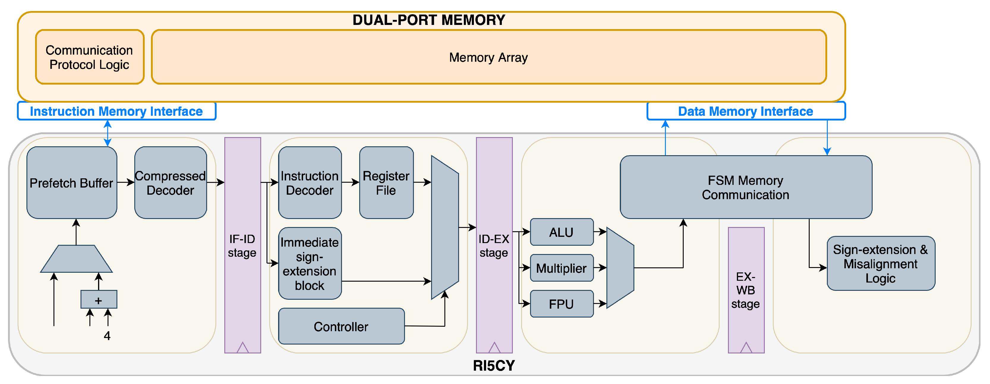
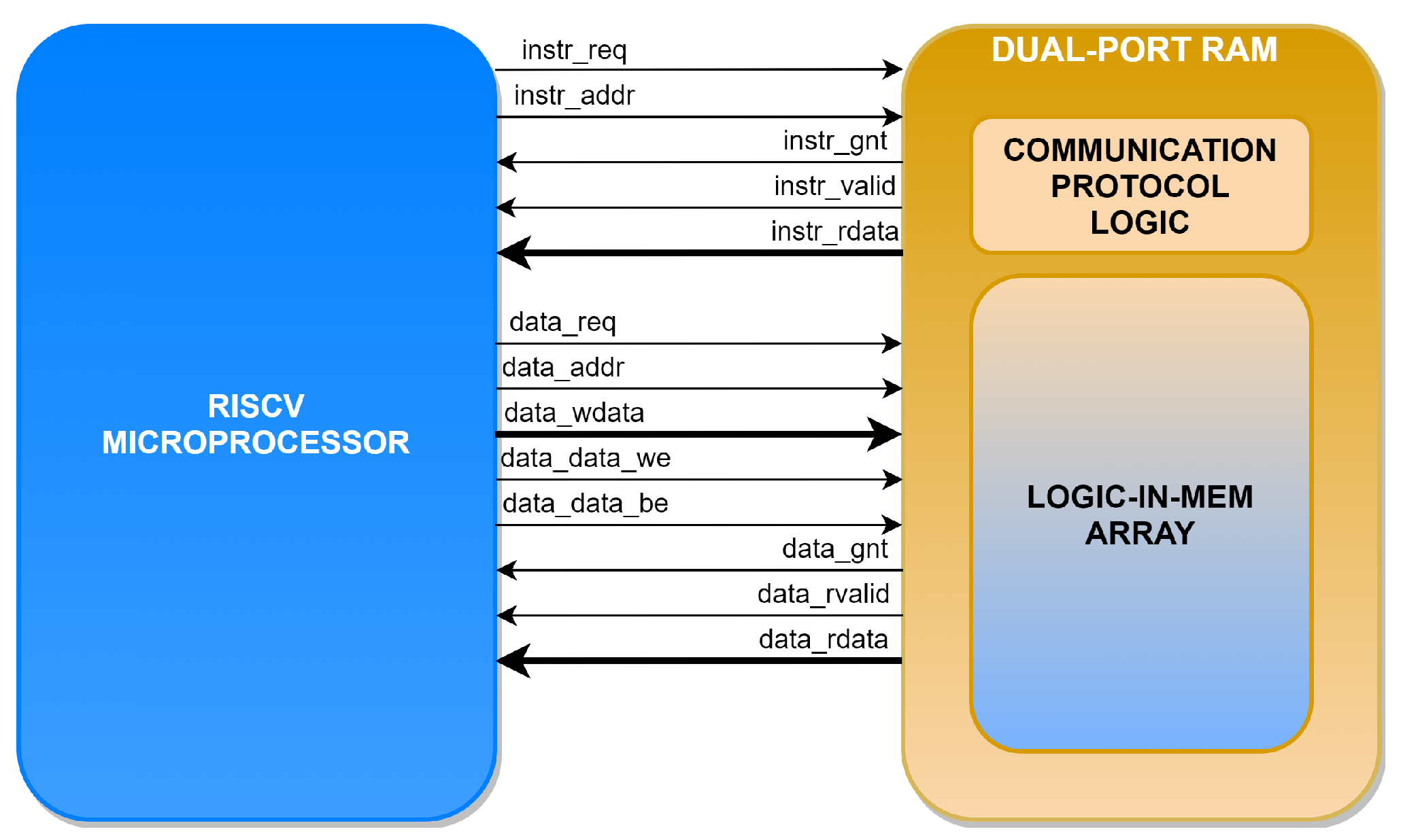
3. Architecture
The case study focuses on the core RI5CY or CV32E40P, a specific RISC-V implementation, developed and maintained by the PULP platform (
https://www.pulp-platform.org/, last accessed on 15 September 2022). As already stated, the RIC5Y core was chosen because of its flexibility that is characteristic of the RISC-V standard family. As in all RISC-V implementations, it is possible to extend the ISA to enable the core to support new customized functionalities. Therefore, the RI5CY core is a good candidate for integration of the LiM concept. RI5CY is a four-stage, in-order 32-bit core [
20].
Figure 1 presents an overview of the RI5CY architecture.
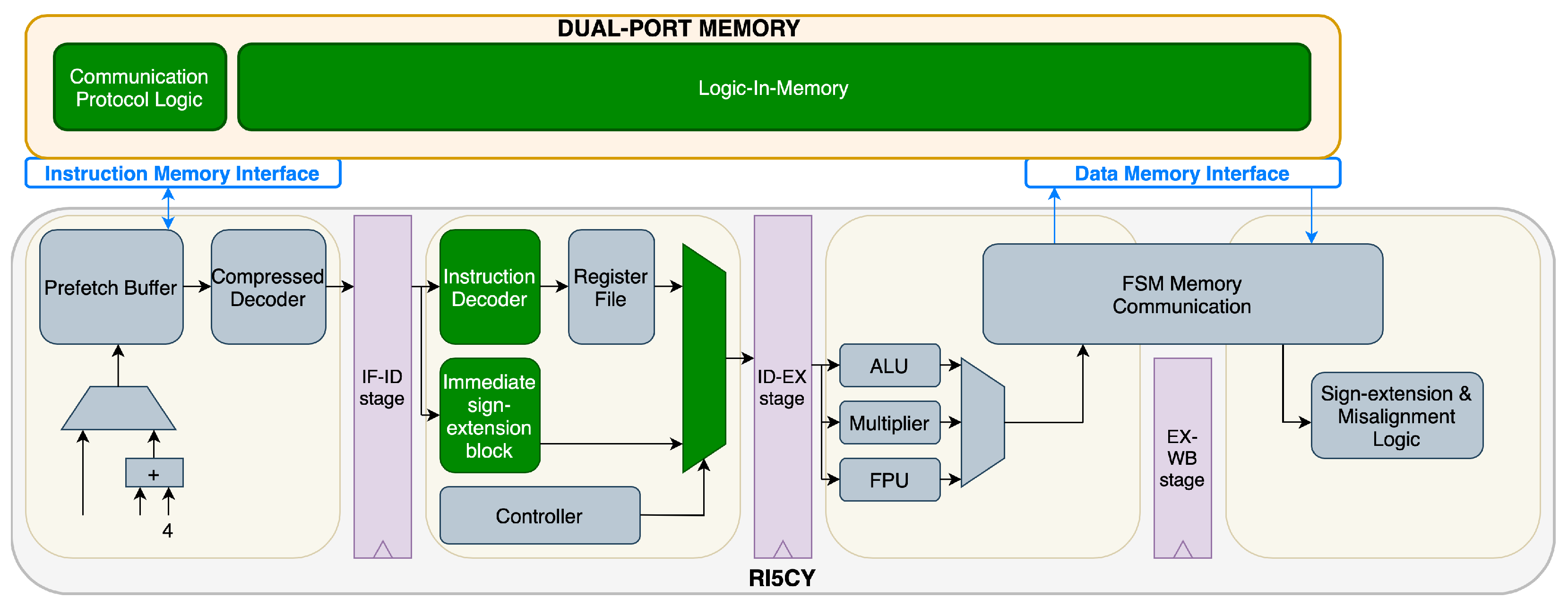
The given memory model is replaced with a LiM model. Additional logic within the RI5CY core is added to support new LiM management instructions.
Figure 2 represents, in green, the significant blocks that are changed with respect to the initial architecture. The framework relies on the existing interface between the processor and the memory. The RI5CY core introduces new instructions to control the new LiM, so the decoder within the instruction fetch stage (IF) is enlarged. At the same time, a new immediate type is required due to the different format of the instructions. Consequently, the sign-extension block is also changed. More details on the interface and the new instructions are presented in the next section, following a full description of the proposed LiM architecture.
4. Test Memory Architecture
The RI5CY core has only one memory for both instructions and data. The instructions and data parts of the memory share the same physical memory and there is no specific address that divides the two parts. The management of the division between them is left to the compiler. Therefore, as for the standard RI5CY memory model, the new architecture involves a dual-port memory, such that fetch and load-store operations can occur in the same clock cycle with two decoders corresponding to the two ports, creating the possibility of addressing all memory locations. In addition, the implemented LiM adds some logic around the memory array and within the memory array itself. The result is a memory capable of performing basic bitwise operations and a few simple algorithms.
In more detail, the proposed memory architecture can perform the following operations:
Normal load and store operations: the new memory can still behave like a memory such that it will perform a read or a write in just one clock cycle. The data port of the memory supports load and store for 8-bit, 16-bit or 32-bit data.
Bitwise operations: Only the data port of the memory can enable the logic for this kind of operation. Load and store can be performed together with a bitwise operation using an input mask, in just one clock cycle, creating a store logic and load logic operation. In the case of a store logic operation, the input of the memory is a mask that is used to perform a logic operation with a selected memory cell. In the case of a load logic operation, the load value is the result of the bitwise operation between a memory cell and an input mask. The available bitwise operations are AND, OR and XOR. In case of a store logic, the bitwise operation is also supported for a range of memory locations, assuming that the input mask used is the same for all locations selected. In this case, the input data is used to perform a bitwise operation on a specific number of memory rows, starting from the address provided to the memory. Bitwise operations are supported only on 32-bit data, on aligned addresses.
Maximum and minimum: a special load operation, max min load enables calculation of the maximum or minimum value for a specific range of memory locations. This memory operation requires 33 clock cycles for any range selected. The maximum and minimum are computed considering 32-bit data values.
This memory model and the type of in-memory logic operations used are based on the solution proposed in [
21]. Here, we use it as an ideal model to test the effectiveness of the proposed framework.
Figure 3 shows the high-level logic-in-memory structure. Due to the non-static distinction between instructions and data memory, the logic introduced for the above-listed operations is distributed over all the memory locations, even if it is effectively used with data and not with instructions.
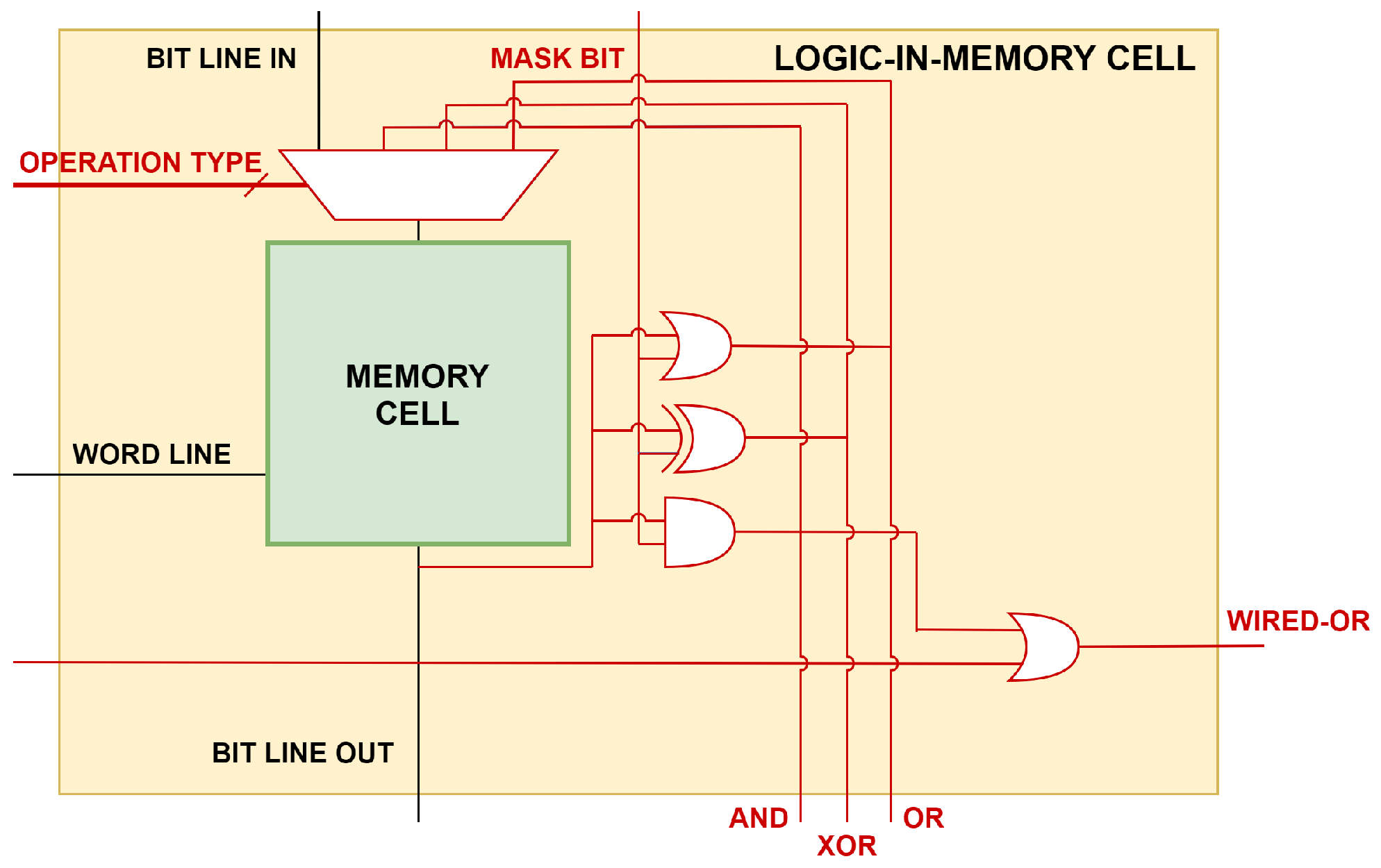
4.1. Bitwise Operations—Logic-in-Memory Cell
The heart of a bitwise operation is the memory bit-cell, shown in
Figure 4. The memory cell is enlarged to compute the bitwise operation between the content of the cell and an input mask bit.
Defining
load logic as the load operation that performs a logic operation, the load logic does not compromise the cell memory content: logic gates, such as AND, OR and XOR, are placed at the output of the memory cell, then on the output bit line. The additional OR port is needed for maximum and minimum computation (more details in
Section 4.2). In a
store logic, instead, the result of the bitwise operation is fed back as input to the cell.
Both load and store logic require just one clock cycle to execute.
4.2. Maximum and Minimum Computation—Logic around the Memory Array
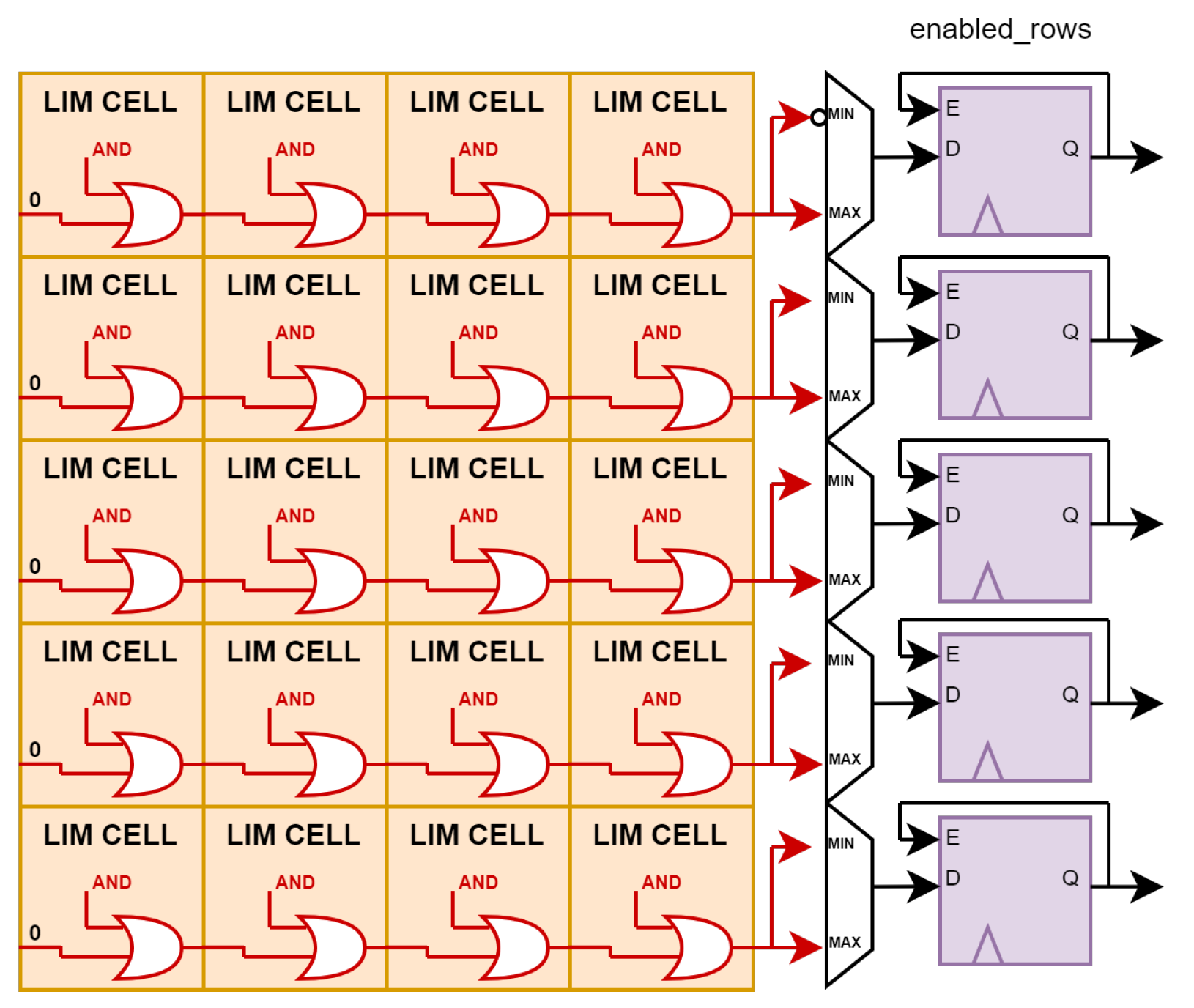
LiM computes the maximum and minimum values with a very straightforward algorithm. In the case of maximum search, the algorithm starts evaluating the MSB of a set of memory words. If at least one MSB is equal to 1, words that have MSB equal to 0 are excluded. The same operation is repeated N times the number of bits of the words considered. The last operation is performed on the LSB. The minimum value computation works in the same way, with the only difference that the exclusion is performed on words where the considered bit is equal to 1 instead of 0.
The implementation of this algorithm is based on [
21] and requires additional logic within the memory cells (
Figure 4) and around the memory array (
Figure 5):
Additional logic around the memory produces a 32-bit mask at each clock cycle that has only one bit set per clock cycle. The initial mask sets the MSB, while the last mask produced sets the LSB.
The 32-bit mask is distributed to groups of four bytes. Therefore the evaluation is performed in parallel in all memory locations involved. The AND gate inside the new memory cell that has as inputs the bit cell content and the input mask gives, as a result, the bit cell content only in the position of the mask bit set to 1. All the other bits are masked with a 0. A 32 bits wired-or between the AND gate outputs is performed by the additional OR gate in the memory cell. The wired-or net gives the value of the bit to evaluate for each four-byte group.
Additional logic around memory completes the one clock cycle step of the algorithm. This part of the logic evaluates the wired-or net corresponding to the words of interest. In the case of maximum computation, words with the wired-or bit equal to 1 are considered in the next cycle. Otherwise, these words are excluded from the comparison. The opposite procedure is performed in the case of minimum computation. The information of the enabled words is stored inside the registers’ enabled_rows and updated cycle by cycle. The initial value of these registers is given by the range address decoder, according to the range of words that are of interest. During execution, only the registers of the enabled_rows equal to 1 can be updated by the wired-or result each cycle. At the end of the algorithm, the enabled word registers that show a 1 correspond to the memory words with the maximum/minimum value.
The complete algorithm requires 33 clock cycles to run—one cycle to initialise the enabled words information and 32 cycles to evaluate 32-bit words. The algorithm requires 33 clock cycles irrespective of the number of words to evaluate because all the steps are performed in parallel between words.
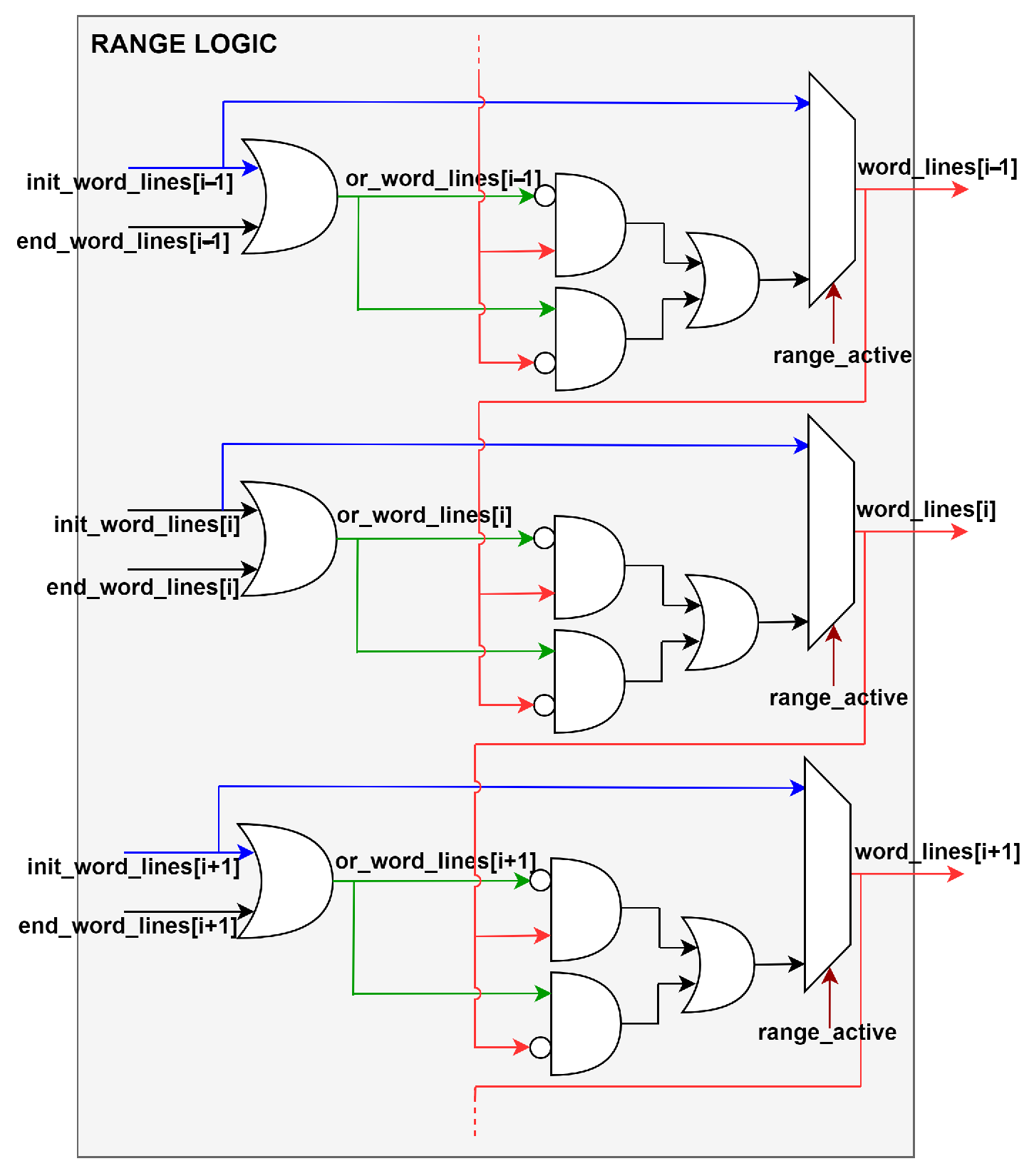
4.3. Range Operations
As previously indicated, the achieved memory architecture can perform operations on a certain range of memory locations. The range operations are:
The range operations require a starting address and involvement of a range of 32-bit words, both provided by the processor. The logic adopted to enable the required word lines is shown in
Figure 6. The range decoder logic requires two standard address decoders, one for the starting address and one for the end address (the end address is computed by adding the range to the starting address). The output of the two decoders is combined so that only the lines in between are effectively activated. In non-range operations, only the starting address is considered and the range logic is bypassed.
5. Interface Bus
The main problem requiring solution in the new architecture was communication between the microprocessor and the new memory. With respect to a basic memory, the LiM requires information about the type of operation to execute, which is not needed in the standard memory-processor interface. We chose a solution that supported the new LiM operations by keeping the same memory interface of the standard RISC-V core. This was to prioritise the flexibility and re-usability of the core in other existing platforms. The communication interface is depicted in
Figure 7. The type of LiM operation is communicated by writing a word in a specific memory location. This enables support of any kind of in-memory operation without the need to change the RISC-V bus.
The characteristics of this interface bus are as follows:
The LiM information on the operation to compute is stored inside one specific memory address. The memory functionality depends on what is written in this memory location, which acts as control logic for the entire memory.
The processor programs the memory by performing a store to this memory address. The processor must provide the information needed using the write-data bus already available from the interface.
Any subsequent load or store is interpreted according to the programmed behaviour in the memory.
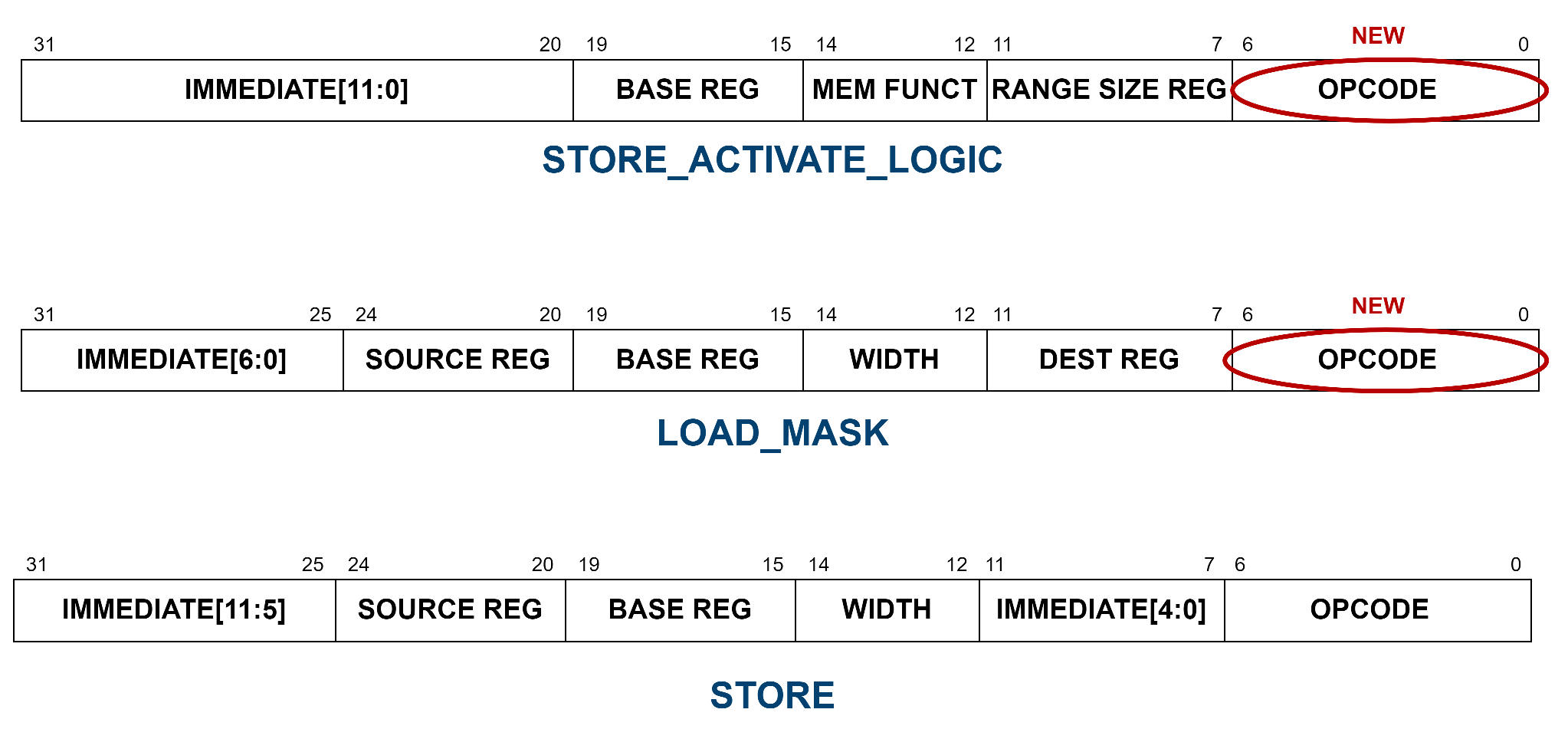
To support this new functionality the RISC-V ISA introduces new instructions (
Figure 8):
STORE_ACTIVATE_LOGIC. This new instruction enables programming of the memory to operate in a certain mode by writing in the specific memory location. The instruction format contains information about the operation type and the range size. These two pieces of information are packed to be sent over the 32-bit write data bus. The implemented operation types are NONE, AND, OR, XOR, MAX, MIN, but the 3-bit mem funct field can support additional operations. The range size reg field should, thus, be used when allowed, indicating the register address from where to read the range size; otherwise, it should be set to 0.
LOAD_MASK. The already available LOAD instruction is not sufficient to perform a logic operation in memory. The base integer ISA load instruction does not allow the input mask to be sent to the memory. The LOAD_MASK instruction is only introduced to read the input mask from the register file through the source reg field. The value read is sent to the memory using the write data bus. The compiler should always place this instruction after the activation of the in-memory logic operations.
STORE. This is not a new instruction for the RISC-V core. The memory interprets a normal store instruction as a logic store instruction if the memory is programmed accordingly. The value read by the source reg register corresponds to the input mask in the case of a logic store, or the data to effectively store in the case of a normal store.
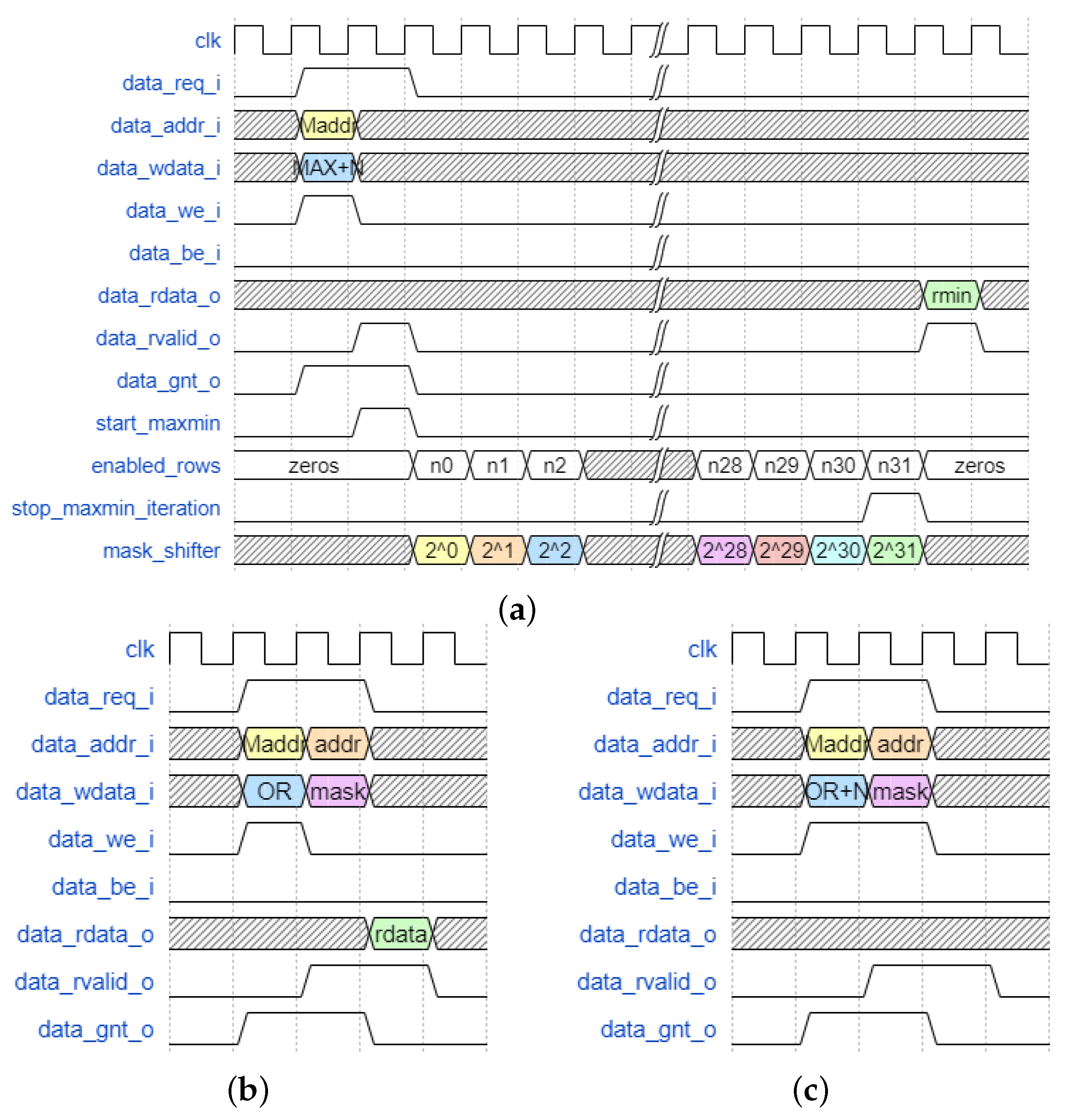
The expected behaviour of the memory interface is illustrated in
Figure 9. In all cases, each LiM operation is preceded by the STORE_ACTIVE_LOGIC. It passes the type of operation and the range of the operation through the
write_data bus. The memory interprets the next load/store instruction according to what is stored in the special address. In the case of max/min computation, additional internal signals are highlighted:
start_maxmin is a pulse signal that launches the max/min specific hardware. In the following cycle, the
enabled_rows assume an initial value (computed according to the starting address and the given range size) and the
mask_shifter is updated, starting by showing the value
to isolate the MSB in the computation; when the mask assumes the value
, this indicates that the LSB is being evaluated, so
stop_maxmin_computation is set to stop the execution.
6. Modified RISC-V Compiler
6.1. Adding Support to the Custom LiM Instructions
To improve the flexibility of the RISC-VLiM system, similarly to what was undertaken in [
22], we modified the original RISC-V compiler, inserting the new custom instructions. Starting from the
riscv-gnu-toolchain (
https://github.com/riscv-collab/riscv-gnu-toolchain, last accessed on 15 September 2022) and using the
RISC-V Opcodes (
https://github.com/riscv/riscv-opcodes, last accessed on 15 September 2022) tool, we were able to insert store_activate_logic and load_mask instructions to the original instruction set. We started by modifying the file
opcodes-rv32i in the
riscv-opcodes repository and inserting the new custom LiM instructions. For example, the sw_active_or instruction is defined as:
![Electronics 11 02990 i001]()
From left to right, the fields composing the instruction indicate the name of the instruction, the operands (rd: destination register; rs1: source register 1; imm12: 12-bits immediate) and the other bits values of the instruction. Considering
Figure 8, the
func field (bits 14 down to 12) is 3 and the opcode field is 0x0E (bits 6 down to 2) and 3 (bits 1 down to 0).
Subsequently, by running the parse_opcodes program, a header file is generated, containing MASK, MATCH, and DECLARE_INSN directives for the new custom instruction, as shown in Listing 1.
| Listing 1. Generated RISCV_ENCODING for sw_active_or instruction. |
![Electronics 11 02990 i002a]() |
![Electronics 11 02990 i002b]() |
At this point, after configuring riscv-gnu-toolchain using the options with-arch=rv32ima and with-abi=ilp32, two files are modified in the riscv-binutils directory. The first is ./include /opcodes/riscv-opc.h, in which the code generated by riscv-opcodes tool (Listing 1) is pasted. The second is ./opcodes/risc-opc.c, where the code lines in Listing 2 are added, specifying the instruction name, its class, the operands, and the match and mask values for the new custom instruction.
| Listing 2. Modified riscv-opc.c file, with sw_active_or custom instruction. |
![Electronics 11 02990 i003]() |
6.2. Writing a Program Exploiting LiM Functionality
Once the toolchain is ready, the user can declare the custom assembly instruction directly inside the C code by means of an
asm volatile statement, as shown in Listing 3. The total number of active memory lines is specified in the destination register (rd) of the custom LiM instruction, i.e., how many rows execute the LiM operation. In the source register 1 (rs1), the configuration address is specified, i.e., the reserved address used to configure the memory function (that, in this case, is an XOR), setting the selector value of the LiM cell multiplexer properly (see (
Figure 4). The immediate value defines the offset to add to the rs1 value. It can be observed that, between the two custom LiM instructions, there is a store operation: after the memory is configured to execute a LiM operation, from the corresponding memory location, with a range specified by rd, the specified logic function is executed, and the result is saved inside the corresponding memory lines. At the end of the LiM part, the standard memory function is restored through
sw_active_none.
| Listing 3. Fragment of C code for the XNOR-Net algorithm. |
![Electronics 11 02990 i004]() |
7. Racetrack Logic: A Case Study
7.1. Racetrack Background
Racetrack memory is a promising storage scheme for the development of high-density storage devices. First proposed by IBM, it is based on magnetic stripes, preferably made of material with perpendicular magnetic anisotropy (PMA) [
23]. The digital information is encoded by the magnetization direction of domains, separated by domain walls [
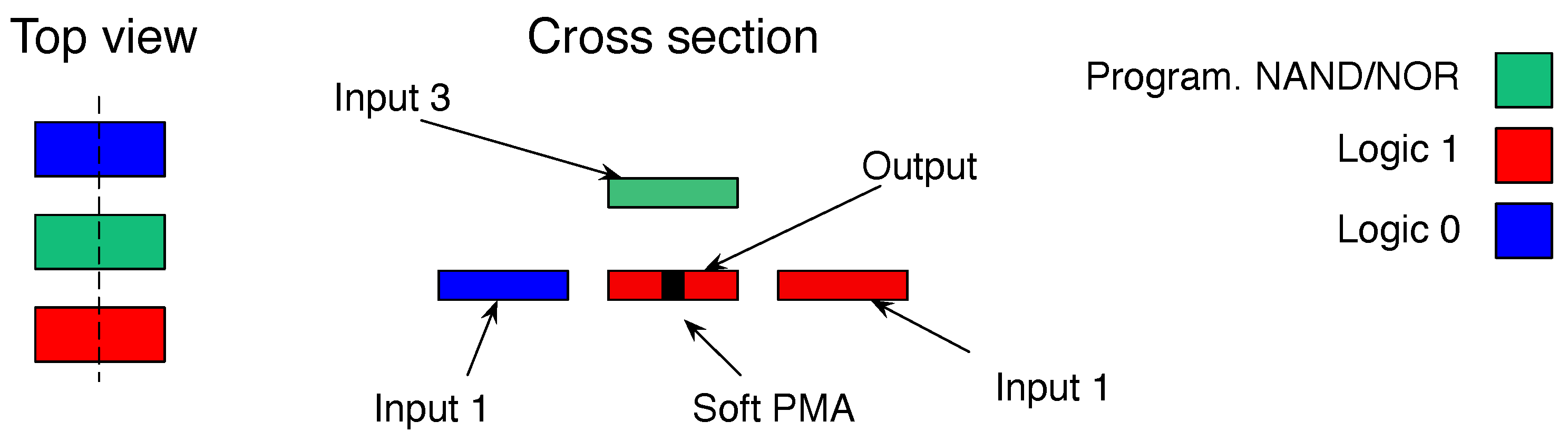
24]. The magnetization pointing downwards represents logic 0, whereas logic 1 is represented by the opposite magnetization. However, the racetrack array can be enriched with computing capabilities by arranging three parallel racetracks and defining a soft PMA spot on every bit of the central track [
25] (see
Figure 10).
The soft PMA spot, located at the center of the output, is more sensitive to the magnetic field variations and, therefore, is where the domain wall nucleates. This spot is tuned by focused ion beam irradiation [
26]. The logic function implemented by the computing cell is
. Therefore, the value of IN3 programs every single cell to operate as NAND or NOR when IN3 is equal to 1 or 0, respectively. The value of the output element is defined by the superposition of the three surrounding inputs and the sign of the external magnetic field. The external field brings the output close to the coercivity field and then the switching is supported or prevented by the value of the surrounded inputs [
27,
28]. The global out-of-plane field can be generated on-chip, sandwiching the magnetic stack between cladding material [
29].
7.2. Memory Implementation
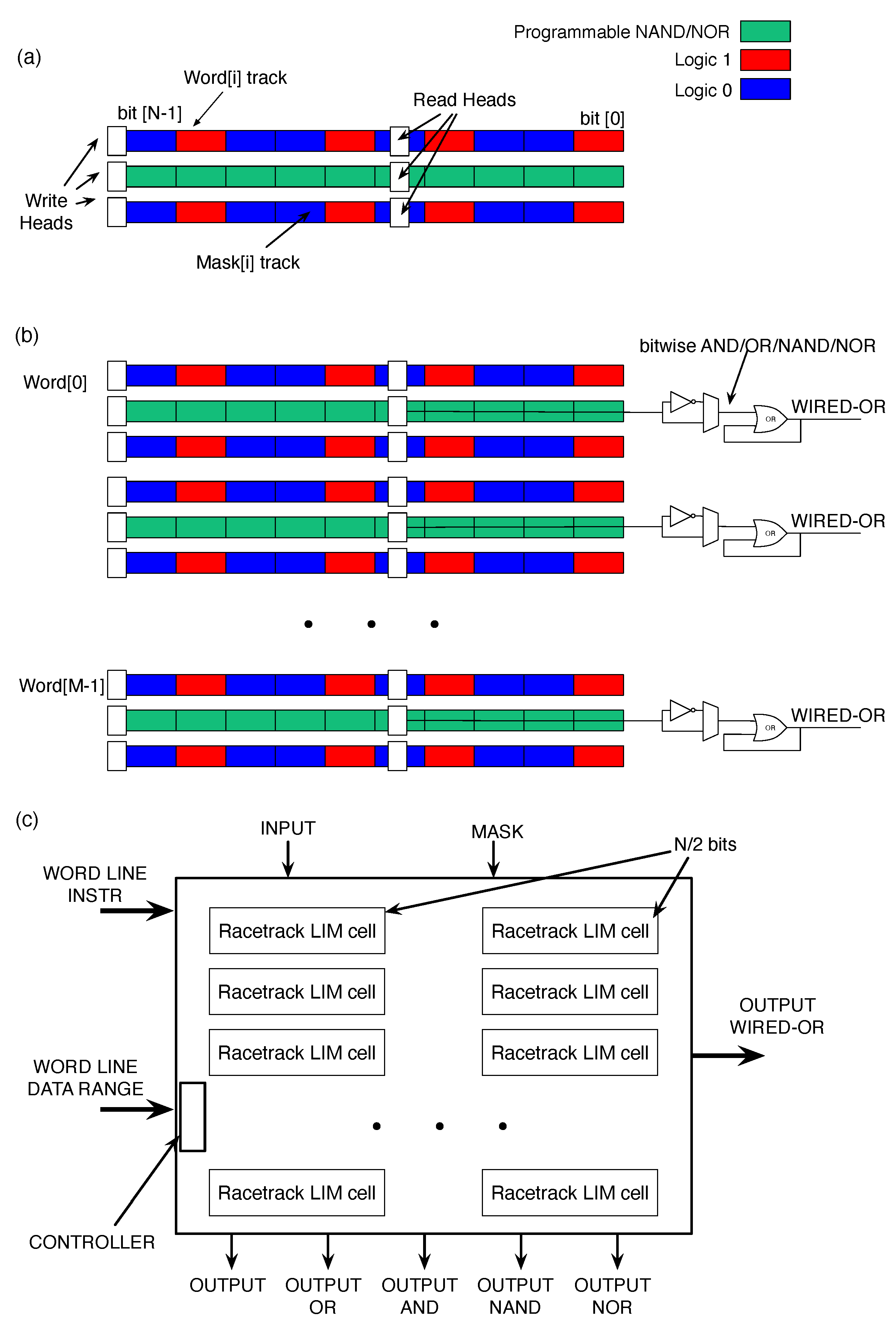
By arranging multiple computing cells, as displayed in
Figure 10, in a track-like structure (
Figure 11a), it is possible to build the computing word line. At least one write and read head are necessary for modifying and accessing the stored data. Two distinct ports are available per track, one for writing and one for reading operations. Domain walls are nucleated by the write head and shifted sequentially by a low current pulse into the in track [
30]. The measured current density for nanosecond long pulses is ≈1 × 10
A/cm
for Co/Pt tracks [
31,
32] and ≈5 × 10
A/cm
for CoFeB/MgO tracks [
33]. Here, racetracks made of CoFeB/MgO are considered. One track is used for storing the memory values. The programmable track defines the logic function implemented in every computing cell. In the third track, it is possible to load the mask for performing bitwise operations.
Figure 11b shows the memory array for M words with N bit parallelism. The schematic representation adds extra CMOS logic only around the memory array. This extra logic results in a racetrack memory able to perform simple bitwise operations, in parallel, over the whole array. In this case study, the LiM array can implement NAND/NOR operations without moving data. The peripheral circuitry is used as support for implementing the AND/OR functions. The output OR makes it possible to perform the wired-or for the minimum and maximum execution of the algorithm over the N output bits. This is the basic building block of the racetrack logic array. It consists of 3M parallel tracks, plus the additional programmable track located above the output. Each track can hold up to N bits and can have up to one access port per reading and one per writing operation. Even if the racetrack memory structure differs from standard memory, the I/O interface is maintained to ease the integration.
The 32-bit data parallelism results in 32 writes and shifts interleaved operations to fill the memory array. The memory controller, depicted in
Figure 11c, is in charge of managing the access to the racetrack memory. It computes the number of shifts to access the data and determines if a bitwise operation needs to be executed. In this memory implementation, the access policy is static. This means that access ports are statically assigned to certain magnetic domains. In the simplest implementation, with N bits parallelism and two distinct write/read heads, every domain is associated with the write/read port. Therefore, up to N shift operations are required to fully load new data in the word line.
In this case study, the memory array is divided into sub-arrays to reduce the number of shift operations, as suggested in [
31]. In this case, the array is split into sub-arrays with N/2 bits reducing the number of shifts by half. Therefore, considering the operating clock frequency of the processor, the write/read and shift operations are included in this time frame to meet the architecture requirements.
8. Results
8.1. Simulation
The first results were collected using the ideal model of the LiM, to analyze the improvements that the new memory architecture would guarantee with respect to a von Neumann system, such as the RI5CY core. The new ISA extensions can generally improve the speed of the RISC-V in terms of execution time because they enable reduction in the number of memory accesses during the execution of a program. A set of programs were written and simulated to demonstrate the efficiency of the two RI5CY LiM-based accelerators.
All the test programs were written in C language and then compiled with the modified RISC-V compiler. The applied methodology for the proposed benchmarks consisted of:
Writing the C program and compiling it with the RISC-V compiler. In this phase, the C program does not include any custom LiM instruction. The result is the program.hex file containing the instructions in machine language. The extensions used are the standard RVI (base integer extension) and RVM (integer multiplication and division extension).
Kicking-off the simulation on the RISC-V system, using the LiM as a normal memory. The simulation results are the baseline for comparison with the LiM-specific instructions.
Implement the C program again, inserting the custom LiM instructions by means of an asm volatile statement.
Initiating the simulation on the RISC-V system with the LiM. This time, the simulation results contain the new ISA extensions.
Comparing the two simulation outcomes.
In the following, the ISA without LiM extension and the ISA with LiM extension are referred to as MEMORY and LiM, respectively.
In order to fully exploit the advantages of the LiM paradigm, a selection of the algorithms was performed according to the following criteria:
High data demand. Applications with high memory content are suitable because the LiM can reduce the data movement to/from memory.
Data manipulation with supported LiM operations. The implemented LiM can perform a limited amount of operations without the need for a microprocessor. An algorithm selection that uses these operations is needed to exploit LiM functionality.
Simple algorithms. Algorithms which are not overly complicated are needed at this stage because the compiler does not support the new LiM ISAs. Simple algorithms avoid the risk of introducing errors during the partial manual compilation.
Two basic programs (called custom programs) were written and tested to verify the functionality. The first program, bitwise.c, performs many bitwise logic operations, while the second program, max_min.c calculates the maximum and minimum values of a given vector. Real-world algorithms were tested too and are referred to as standard algorithms. These algorithms were:
bitmap_search.c. A bitmap index searching algorithm. A bitmap index is a special kind of data structure that uses bitmaps to speed up the processing of stored data.
aes128_arkey.c. This algorithm implements part of the advanced encryption standard, the AddRoundKey step, which is performed 11 times in the whole encryption process. The AddRoundKey consists of XOR operations between the bytes of the states matrix and the key matrix, element by element. The result is the next states matrix used for the subsequent steps that lead to the encryption.
transport_cost.c. The transport problem is an algorithm that minimises the cost of distributing a product from a number of sources or origins to a number of destinations.
xnor_net.c. XNOR-Net [
16,
34] is a binary neural network model that enables reduction in computation complexity by approximating weights-inputs to only two values (−1, +1), based on their signs. The value of −1 is associated with logic ’0’ and +1 to logic ’1’. This approximation reduces the convolution into XNOR bitwise and pop-counting operations. The pop-counting consists of the difference between the number of ones and zeros inside a bitstream. The proposed LiM approach enables computation of the XOR in parallel while the processor executes pop-counting. However, due to a very long simulation time, we implemented only one convolutional layer with an input of 28 × 28 pixels (size of the MNIST dataset) and a filter of 5 × 5. This required a simulation time of several hours with Synopsys VCS.
Table 1 compares the execution time of a particular algorithm for all the versions implemented, where cc stands for clock cycles.
The RI5CY processor with the LiM instructions showed an improvement of more than 20% in the case of the custom programs. The improvement was relatively great because the programs were tailored to take advantage of the new LiM instructions. However, this is still a significant result, since it demonstrates the upper bound of the improvement allowed by the LiM. The simulation results for the standard programs were, however, as expected, different, but, in general, still showed an improvement in the execution time. The XNOR-Net case showed a slight speed improvement, but, in terms of execution time, there was a reduction of 3449 clock cycles. This result indicates that, for more complex neural networks with several convolutional and fully connected layers, use of LiM results in remarkable reduction in the execution time for complex and highly parallelizable algorithms, as shown by
Table 1. Due to a very long simulation time, it was necessary to reduce the program complexity, but, in general, real-world programs work with vast amounts of data, so the new logic-in-memory ISA extensions would perform even better in that context. In
Table 2, a comparison of the number of memory accesses between memory and LiM cases is presented. As can be seen, there was a reduction in memory operations for almost all benchmarks, except for bitmap_search. This benchmark was developed based on a tiny number of entries, resulting in inefficiency for LiM. However, even considering bitmap_search, the trend was positive because, for more complex algorithms (such as max/min computation or xnor_net), the LiM paradigm enabled reduction in the effect of the memory wall, by employing parallel computation and reducing the communication between CPU and memory.
8.2. CMOS-Based Performance Evaluation Flow
In the simulation section, an indication of the improvement in execution time achievable with a LiM solution was provided. Here we define a method to evaluate the performance (i.e., power, area, energy and timing) for both the standard and LiM solutions. For the standard memory case, we use the classical digital design flow that starts with a description of the architecture in HDL language, continues with the synthesis using the Synopsys Design compiler and, finally, ends with place and route using Cadence Innovus. Unfortunately, if this flow had also been used in the LiM case, the results would have been unreliable. The proposed custom LiM cell (in
Figure 4) would have been implemented using the elements provided by the CMOS library, which would have been very inefficient as well as very far from the custom nature of the cell. For these reasons, additional steps were proposed for the LiM case:
The LiM cell is designed at the transistor level and tested with Cadence Virtuoso.
Once the functionality is proven, a layout view of the cell is created and simulated again. The layout view enables taking into account parasitic effects in the performance estimations.
DRC (design rule check), LVS (layout-vs.-schematic) and PEX (parasitic extraction) procedures are executed on the layout view. At the end of the PEX process, a Spectre netlist is generated, containing the description of the LiM cell with both transistor and parasitic elements.
Cadence Liberate characterizes the LiM cell. This step takes in input from the Spectre netlist and transistor models and provides a Liberty file containing power, area and timing values of the cell. This file is compatible with the Synopsys Design compiler for the synthesis process.
Abstract view and library exchange format (LEF) file generation of the LiM cell. These can be obtained from the layout view with Cadence Abstract. The LEF file is used by Cadence Innovus to perform the automatic place and route step. The abstract view, described in the LEF file, contains only the I/O pins, cell boundary and metal obstruction information.
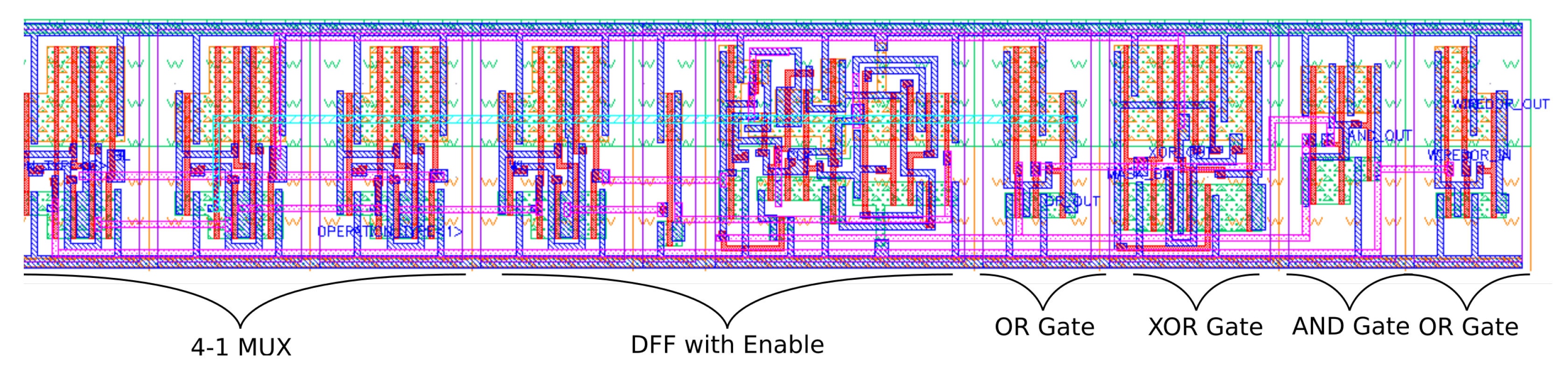
The LiM cell layout is reported in
Figure 12. Both Standard and LiM flows are based on the FreePDK 45 nm CMOS technology. At the end of the LiM procedure, the Liberty file is compiled with Library Compiler by Synopsys and the new custom library is ready to be used.
8.2.1. Synthesis and Place and Route
This subsection compares LiM and standard solutions for power, area, energy, and critical path. The results obtained after synthesis and place and route procedures of an entire memory array made of LiM cells (depicted in
Figure 4) are compared with those obtained in the case of standard memory. The synthesis process is exploited considering the Liberty file generated by Cadence Liberate, obtained in the fourth step in
Section 8.2. The
.lib file is compiled with the Library Compiler tool by Synopsys, producing a database file with extension
.db, compatible with the Synopsys Design compiler used for the synthesis. Two top-level VHDL files describe the structures of the memories, the LiM and the standard files, respectively. The Design Compiler analyzes and synthesizes these files, producing two netlists of the two memories. After that, Innovus is exploited to perform the place and route procedure for both memories: it takes as input the netlists and structures of the floorplans; performs the placement of the standard/custom cells and fillers on the chips; connects the cells to the supply rails; places the I/O pins; performs the clock-tree synthesis, and finally routes the entire design. At the end of the routing phase, the design is ready to be simulated; the performance can be precisely evaluated since Innovus saves the parasitic contributions of the interconnections and the cells. Both memories use a D flip-flop with enable (DFFEn) as a basic cell and have a size of 1024 rows × 32 bits of parallelism. In the standard memory case, the DFFEn is implemented with a simple D flip-flop (DFF), an inverter and a 2-1 multiplexer. We are aware that using a D flip-flop as a basic memory element is not optimal, but this investigation seeks to understand the relative difference in performance between a normal memory and a memory with logic elements. For this reason, we chose a D flip-flop as a memory element since it enables embedding of the memory in a standard synthesis performed with Synopsys and Innovus. The results are shown in
Table 3. Due to the choice made regarding the memory implementation, these results represent a worst-case performance analysis. However, it is sufficient to highlight the differences between a memory circuit and a memory circuit capable of performing logic operations on stored data.
As expected, the area and critical path results were worse in the LiM case because of the higher amount of logical elements required in the design. On the other hand, power was lower in the LiM case, since the optimized layout of the LiM cell (shown in
Figure 12) keeps close to the elements. Even when the place and route in the standard memory case was performed without flattening the hierarchy, the LiM case was found to be more efficient. Consequently, the interconnections were shorter than the standard memory, translating to a power reduction. In this particular case, we obtained a power reduction, but this may not necessarily be true with other LiM solutions. The purpose of this framework was to enable comparison of von Neumann architectures with several possible LiM solutions, to verify if they did or did not result in an improvement when inserted in a realistic computing architecture. A comparison between the dissipated energies was considered to evaluate the impact of the LiM paradigm. The energy refers to both the power consumption of the architecture and the execution time of the algorithm, and, hence, provides a complete description of system performance. For the cases analyzed (MEMORY and LiM), only the energy consumption of the memories was considered, which was computed as follows:
For each architecture, the number of memory operations can be found in
Table 2, while the clock period is fixed to 3 ns.
As shown in
Table 4, LiM reduced the energy consumption by at least ∼43% because of both the significant impact of the custom layout on power consumption and general reduction in the memory operations, as shown in
Table 2. This comparison highlights how the LiM paradigm implemented with CMOS technology can improve system performance, particularly for algorithms suitable for acceleration by a LiM solution, implying a reduction in both energy and execution time.
8.3. Racetrack Implementation
In
Section 7, only the LiM array of the architecture implemented using the racetrack technology was considered. A schematic representation of the memory is shown in
Figure 11c, where each bit has a footprint of 200 × 80 nm. With an inter-track space of 15 nm and 32 bits per word, it is possible to obtain the occupation of each word line. In our implementation, the word line is split by half, with 16 bits for every racetrack LiM cell. Therefore, every 16-bit word line has a footprint of 0.86
m
. In the synthesis reported in
Section 8.2.1, the memory had 1024-word lines of 32 bits each. As a consequence, the overall footprint of the racetrack memory was 1761.3
m
, which was ∼99.8% less than for CMOS. This area does not take into account extra simple logic at the output of every word line and the memory controller. Experimental data presented in [
29,
35,
36] showed that switching the field below 25 mT can be achieved in a Co/Pt multi-layer and even lower for CoFeB/MgO thin films. The on-chip clocking system, required to generate the out-of-plane field to globally operate the racetrack logic array, can reach 300 MHz with homogeneous field distribution with a superalloy cladding material [
29]. From the COMSOL simulations of the clocking structure presented in [
29], the power dissipation stayed below 2 mW, with a computing memory array operating frequency of 300 MHz. Another contribution to the power dissipation results from the data movement inside the memory array. Here, the worst case scenario was considered for the calculations, i.e., where the entire memory needs to be loaded with new values. This means that the input racetracks are loaded simultaneously. The power required to accomplish this operation was 4.65 mW. It is worth noting that the racetrack memory does not show any static power consumption, due to its non-volatile properties.
In
Table 5, a comparison in terms of energy consumption between CMOS and racetrack LiM arrays is presented. As expected, the racetrack technology produced a strong reduction in energy consumption, while the execution time of the algorithms remained unaltered. The results presented here do not take into accunt the extra CMOS logic circuits around the memory array, as, up to now, we have not had the tools to design and test a hybrid racetrack/CMOS circuit, so they may be considered as a best-case scenario. However, the biggest component of the energy consumption was due to the memory array, considering that, in some operations, all memory cells were activated at once. Consequently, the results highlighted here not only demonstrate the validity of the framework that we have developed, but also demonstrate that, with a suitable technology solution, it is possible to create efficient systems in which logic operations can be performed inside the memory.
9. Conclusions
RISC-Vlim is a powerful framework that enables the design of processing systems based on LiM solutions. By moving part of the computation in memory, it is possible to relax the constraints on the logic processor, producing a system without penalties on performance. The case study proposed highlights the potential of this framework, which can also be used to compare different LiM solutions. LiM represents a promising technique for reducing the energy consumption of a von Neumann architecture, by at least 43% in CMOS technology in the proposed benchmarks, as well as reducing memory operations and parallelizing part of the code. Moreover, using the racetrack emerging technology, a further significant reduction in energy of 98% compared to standard CMOS can be achieved, demonstrating that this is an efficient technology for LiM applications. In future investigations, we intend to focus on exploring architecture designs that can further exploit this framework to improve the performance of computing systems.
Author Contributions
Investigation, A.I.; methodology, A.C.; project administration, M.O. and M.V.; resources, M.R.R.; supervision, M.O. and M.V.; validation, A.C. and F.R.; writing—original draft, A.I.; writing—review and editing, A.C., F.R. and M.V. All authors have read and agreed to the published version of the manuscript.
Funding
This research received no external funding.
Data Availability Statement
Not applicable.
Conflicts of Interest
The authors declare no conflict of interest.
References
- Vacca, M.; Graziano, M.; Ottavi, M. Racetrack logic. Electron. Lett. 2017, 53, 1462–1464. [Google Scholar] [CrossRef]
- Santoro, G.; Turvani, G.; Graziano, M. New Logic-In-Memory Paradigms: An Architectural and Technological Perspective. Micromachines 2019, 10, 368. [Google Scholar] [CrossRef] [PubMed]
- Akin, B.; Franchetti, F.; Hoe, J.C. Data Reorganization in Memory Using 3D-Stacked DRAM. SIGARCH Comput. Archit. News 2015, 43, 131–143. [Google Scholar] [CrossRef]
- Kim, D.H.; Athikulwongse, K.; Healy, M.B.; Hossain, M.M.; Jung, M.; Khorosh, I.; Kumar, G.; Lee, Y.; Lewis, D.L.; Lin, T.; et al. Design and Analysis of 3D-MAPS (3D Massively Parallel Processor with Stacked Memory). IEEE Trans. Comput. 2015, 64, 112–125. [Google Scholar] [CrossRef]
- Xie, C.; Song, S.L.; Wang, J.; Zhang, W.; Fu, X. Processing-in-Memory Enabled Graphics Processors for 3D Rendering. In Proceedings of the 2017 IEEE International Symposium on High Performance Computer Architecture (HPCA), Austin, TX, USA, 4–8 February 2017; pp. 637–648. [Google Scholar] [CrossRef]
- Kaplan, R.; Yavits, L.; Ginosar, R.; Weiser, U. A Resistive CAM Processing-in-Storage Architecture for DNA Sequence Alignment. IEEE Micro 2017, 37, 20–28. [Google Scholar] [CrossRef]
- Imani, M.; Gupta, S.; Arredondo, A.; Rosing, T. Efficient query processing in crossbar memory. In Proceedings of the 2017 IEEE/ACM International Symposium on Low Power Electronics and Design (ISLPED), Taipei, Taiwan, 24–26 July 2017; pp. 1–6. [Google Scholar] [CrossRef]
- Giulia, S. Exploring New Computing Paradigms for Data-Intensive Applications. Ph.D. Thesis, Politecnico di Torino, Turin, Italy, 2019. [Google Scholar]
- Angizi, S.; He, Z.; Fan, D. PIMA-Logic: A Novel Processing-in-Memory Architecture for Highly Flexible and Energy-Efficient Logic Computation. In Proceedings of the 2018 55th ACM/ESDA/IEEE Design Automation Conference (DAC), San Francisco, CA, USA, 24–28 June 2018; pp. 1–6. [Google Scholar] [CrossRef]
- Han, L.; Shen, Z.; Shao, Z.; Huang, H.H.; Li, T. A novel ReRAM-based processing-in-memory architecture for graph computing. In Proceedings of the 2017 IEEE 6th Non-Volatile Memory Systems and Applications Symposium (NVMSA), Hsinchu, Taiwan, 16–18 August 2017; pp. 1–6. [Google Scholar] [CrossRef]
- Krestinskaya, O.; James, A.P. Binary weighted memristive analog deep neural network for near-sensor edge processing. In Proceedings of the 2018 IEEE 18th International Conference on Nanotechnology (IEEE-NANO), Cork, Ireland, 23–26 July 2018; pp. 1–4. [Google Scholar]
- Wang, X.; Zidan, M.A.; Lu, W.D. A Crossbar-Based In-Memory Computing Architecture. IEEE Trans. Circuits Syst. I Regul. Pap. 2020, 67, 4224–4232. [Google Scholar] [CrossRef]
- Roohi, A.; Angizi, S.; Fan, D.; DeMara, R.F. Processing-in-memory acceleration of convolutional neural networks for energy-effciency, and power-intermittency resilience. In Proceedings of the 20th International Symposium on Quality Electronic Design (ISQED), Santa Clara, CA, USA, 6–7 March 2019; pp. 8–13. [Google Scholar]
- Rakin, A.S.; Angizi, S.; He, Z.; Fan, D. PIM-TGAN: A Processing-in-Memory Accelerator for Ternary Generative Adversarial Networks. In Proceedings of the 2018 IEEE 36th International Conference on Computer Design (ICCD), Orlando, FL, USA, 7–10 October 2018; pp. 266–273. [Google Scholar]
- Karunaratne, G.; Le Gallo, M.; Cherubini, G.; Benini, L.; Rahimi, A.; Sebastian, A. In-memory hyperdimensional computing. Nat. Electron. 2020, 3, 327–337. [Google Scholar] [CrossRef]
- Coluccio, A.; Vacca, M.; Turvani, G. Logic-in-memory computation: Is it worth it? A binary neural network case study. J. Low Power Electron. Appl. 2020, 10, 7. [Google Scholar] [CrossRef]
- Jarollahi, H.; Onizawa, N.; Gripon, V.; Sakimura, N.; Sugibayashi, T.; Endoh, T.; Ohno, H.; Hanyu, T.; Gross, W.J. A Nonvolatile Associative Memory-Based Context-Driven Search Engine Using 90 nm CMOS/MTJ-Hybrid Logic-in-Memory Architecture. IEEE J. Emerg. Sel. Top. Circuits Syst. 2014, 4, 460–474. [Google Scholar] [CrossRef]
- Yang, K.; Karam, R.; Bhunia, S. Interleaved logic-in-memory architecture for energy-efficient fine-grained data processing. In Proceedings of the 2017 IEEE 60th International Midwest Symposium on Circuits and Systems (MWSCAS), Boston, MA, USA, 6–9 August 2017; pp. 409–412. [Google Scholar] [CrossRef]
- Waterman, A.; Lee, Y.; Patterson, D.A.; Asanovic, K. The RISC-V Instruction Set Manual Volume I: User-Level ISA; EECS Department, University of California: Berkeley, CA, USA, 2016. [Google Scholar]
- Traber, A.; Gautschi, M.; Schiavone, P.D. RI5CY: User Manual; Micrel Lab and Multitherman Lab University of Bologna: Bologna, Italy; Integrated Systems Lab ETH: Zürich, Switzerland, 2019. [Google Scholar]
- Vacca, M.; Tavva, Y.; Chattopadhyay, A.; Calimera, A. Logic-In-Memory Architecture For Min/Max Search. In Proceedings of the 2018 25th IEEE International Conference on Electronics, Circuits and Systems (ICECS), Bordeaux, France, 9–12 December 2018; pp. 853–856. [Google Scholar] [CrossRef]
- Altınay, Ö.; Örs, B. Instruction Extension of RV32I and GCC Back End for Ascon Lightweight Cryptography Algorithm. In Proceedings of the 2021 IEEE International Conference on Omni-Layer Intelligent Systems (COINS), Barcelona, Spain, 23–25 August 2021; pp. 1–6. [Google Scholar]
- Parkin, S.; Yang, S.H. Memory on the racetrack. Nat. Nanotechnol. 2015, 10, 195–198. [Google Scholar] [CrossRef]
- Parkin, S.S.P.; Hayashi, M.; Thomas, L. Magnetic Domain-Wall Racetrack Memory. Science 2008, 320, 190–194. [Google Scholar] [CrossRef] [PubMed]
- Riente, F.; Turvani, G.; Vacca, M.; Graziano, M. Parallel Computation in the Racetrack Memory. IEEE Trans. Emerg. Top. Comput. 2021, 10, 1216–1221. [Google Scholar] [CrossRef]
- Eichwald, I.; Breitkreutz, S.; Ziemys, G.; Csaba, G.; Porod, W.; Becherer, M. Majority logic gate for 3D magnetic computing. Nanotechnology 2014, 25, 335202. [Google Scholar] [CrossRef]
- Ziemys, G.; Trummer, C.; Gamm, S.B.v.; Eichwald, I.; Schmitt-Landsiedel, D.; Becherer, M. Characterization of the magnetization reversal of perpendicular Nanomagnetic Logic clocked in the ns-range. AIP Adv. 2016, 6, 056404. [Google Scholar] [CrossRef] [Green Version]
- Turvani, G.; Riente, F.; Plozner, E.; Vacca, M.; Graziano, M.; Gamm, S.B. A pNML Compact Model Enabling the Exploration of Three-Dimensional Architectures. IEEE Trans. Nanotechnol. 2017, 16, 431–438. [Google Scholar] [CrossRef]
- Becherer, M.; Kiermaier, J.; Breitkreutz, S.; Eichwald, I.; Žiemys, G.; Csaba, G.; Schmitt-Landsiedel, D. Towards on-chip clocking of perpendicular Nanomagnetic Logic. Solid-State Electron. 2014, 102, 46–51. [Google Scholar] [CrossRef]
- Zhao, W.S.; Zhang, Y.; Trinh, H.; Klein, J.; Chappert, C.; Mantovan, R.; Lamperti, A.; Cowburn, R.P.; Trypiniotis, T.; Klaui, M.; et al. Magnetic domain-wall racetrack memory for high density and fast data storage. In Proceedings of the 2012 IEEE 11th International Conference on Solid-State and Integrated Circuit Technology, Xi’an, China, 29 October–1 November 2012; pp. 1–4. [Google Scholar] [CrossRef]
- Bläsing, R.; Khan, A.A.; Filippou, P.C.; Garg, C.; Hameed, F.; Castrillon, J.; Parkin, S.S.P. Magnetic Racetrack Memory: From Physics to the Cusp of Applications Within a Decade. Proc. IEEE 2020, 108, 1303–1321. [Google Scholar] [CrossRef]
- Ryu, K.S.; Thomas, L.; Yang, S.H.; Parkin, S. Chiral spin torque at magnetic domain walls. Nat. Nanotechnol. 2013, 8, 527–533. [Google Scholar] [CrossRef]
- DuttaGupta, S.; Fukami, S.; Kuerbanjiang, B.; Sato, H.; Matsukura, F.; Lazarov, V.K.; Ohno, H. Magnetic domain-wall creep driven by field and current in Ta/CoFeB/MgO. AIP Adv. 2017, 7, 055918. [Google Scholar] [CrossRef]
- Rastegari, M.; Ordonez, V.; Redmon, J.; Farhadi, A. Xnor-net: Imagenet classification using binary convolutional neural networks. In Computer Vision—ECCV 2016, Proceedings of the 14th European Conference, Amsterdam, The Netherlands, 11–14 October 2016; Springer: Cham, Switzerland, 2016; pp. 525–542. [Google Scholar]
- Riente, F.; Mendisch, S.; Gnoli, L.; Ahrens, V.; Roch, M.R.; Becherer, M. Ta/CoFeB/MgO analysis for low power nanomagnetic devices. AIP Adv. 2020, 10, 125229. [Google Scholar] [CrossRef]
- Mendisch, S.; Riente, F.; Ahrens, V.; Gnoli, L.; Haider, M.; Opel, M.; Kiechle, M.; Ruo Roch, M.; Becherer, M. Controlling Domain-Wall Nucleation in Ta/Co-Fe-B/MgO Nanomagnets via Local Ga+ Ion Irradiation. Phys. Rev. Appl. 2021, 16, 014039. [Google Scholar] [CrossRef]
| Publisher’s Note: MDPI stays neutral with regard to jurisdictional claims in published maps and institutional affiliations. |
© 2022 by the authors. Licensee MDPI, Basel, Switzerland. This article is an open access article distributed under the terms and conditions of the Creative Commons Attribution (CC BY) license (https://creativecommons.org/licenses/by/4.0/).


 ,
, 


