
Quasi-BIC-Based High-Q Perfect Absorber with Decoupled Resonant Wavelength and Q Factor


1
State Key Laboratory of Modern Optical Instrumentation, College of Optical Science and Engineering, Zhejiang University, Hangzhou 310024, China
2
Department of Physics, Medi-Caps University, Indore 453331, India
*
Author to whom correspondence should be addressed.
Electronics 2022, 11(15), 2313; https://doi.org/10.3390/electronics11152313
Submission received: 8 June 2022
/
Revised: 16 July 2022
/
Accepted: 23 July 2022
/
Published: 25 July 2022
(This article belongs to the Special Issue Feature Papers in the Optoelectronics Section)
Abstract
:The Q factor in a quasi-BIC-based optical device can approach infinity and has therefore been attracting the attention of many researchers in recent years. However, this mode is barely applied to absorbers since it mainly tunes the radiative loss. The resonant wavelength of quasi-BICs normally couples with the Q factor, and it is difficult to independently tune one of them while maintaining the other, which weakens the flexibility of tuning. In this work, a quasi-BIC-based high-Q perfect absorber with some unique features is proposed. It shows a decoupled relationship between the resonant wavelength and the Q factor such that these two properties can be independently tuned by changing different structure parameters. In addition, both radiative and resistive losses are tunable. An easy method is proposed to design a perfect absorber with different resonant wavelengths and different Q factors, and a near-infrared perfect absorber with a Q factor as high as 5.13 × 10⁵ is designed. This work proposes a method to tune the quasi-BIC mode, thereby introducing a new paradigm for the design of a high-Q perfect absorber.
1. Introduction
A high-Q factor means a long photon lifetime and good coherence, which suggests high accuracy and high quality in practical applications. High-Q devices have been attracting the attention of many researchers for decades and are extensively applied in the fields of sensing [1,2], lasing [3], filtering [4], information transfer [5], nonlinear harmonics generations [6], energy manipulation [7], and so on. High-Q absorbers can be used in sensors [8] and monochromatic photoelectric detectors [9]. In the infrared range, high-Q absorbers can also work as a high-Q infrared source [10] since absorptivity is equal to emissivity according to Kirchhoff’s law of thermal radiation. High-Q absorbers can be realized by using photonic crystals [11], Tamm plasmonic structures [12], surface plasmon polariton (SPP) [13], surface phonon polariton (SPhP) [14], Bragg gratings [15], and so on.
Bound states in the continuum (BICs) [16,17] are special electromagnetic states that are confined in photonic structures and cannot radiate to the far field, even though they coexist with a continuous spectrum that can carry energy away. They can exist in various photonic structures, e.g., metasurfaces [18,19], plasmonic structures [20,21], photonic crystals [22,23], and fiber Bragg gratings [24]. BICs can be generally divided into three categories—symmetry-protected BICs [25,26], single-resonance parametric BICs [27], and coupled resonance induced BICs [28,29]. The symmetry-protected BICs exist in a system exhibiting a reflection or rotational symmetry. The single-resonance parametric BICs can be evolved from a single resonance when enough parameters are tuned. The coupled resonance induced BICs originate from the coupling between two or more resonances in the system.
Quasi-BICs are often evolved from coupled resonance induced BICs (e.g., Fano resonances [30,31] and Mie resonances [32,33]), where the infinite radiative Q degrades to a finite value. In most works, the resonances forming quasi-BICs share the same optical cavity and are simultaneously tuned when changing the structure parameters [34,35], so the resonant wavelength and the Q factor change together during the process; i.e., the resonant wavelength is coupled with the Q factor in the quasi-BIC system, which weakens the flexibility of tuning. Since they are mainly used to tune radiative loss, current quasi-BICs are often applied in reflectors or transmitters [36,37] and barely in absorbers.
In this work, a quasi-BIC-based high-Q perfect absorber is proposed by using the coupling between a guided mode and a Fabry–Perot (FP) mode. The resonant wavelength and the Q factor of the quasi-BIC mode are decoupled and can be tuned independently. Both resistive and radiative losses can be tuned in the structure. An easy method to design a perfect absorber with different resonant wavelengths and different Q factors is proposed. A near-infrared perfect absorber with a Q factor as high as 5.13 × 10⁵ is designed by using this method.
2. Methods
Simulations are conducted in commercial software COMSOL 5.4.
Simulation of absorptivity: Cross-section of a single period was built in COMSOL 5.4, with air layers upon the structure. “Electromagnetic Waves, Frequency Domain” and “Frequency Domain” were chosen for “Physics” and “Study” parts, respectively. Periodic boundary condition was set for lateral boundaries. The top air layer was set as a perfectly matched layer (PML). The bottom boundary of the PML was set as a port to emit light to the structure. After setting the material parameters (relative permittivity, relative permeability, and electrical conductivity), meshing, and scanning parameters, calculations were conducted. Finally, reflectivity R can be calculated by taking square of S-parameter S11, and absorptivity can be obtained by 1−R since there is no transmission in the system.
Simulation of eigenmode: Model building, boundary conditions, and “Physics” were the same as the simulation of absorptivity above, except that there was no need of a port. “Eigenfrequency” was chosen for the “Study” part. For the simulation of radiative loss, the imaginary part of relative permittivity should be set as 0, and in this case, the energy loss in the system is the radiative loss. For the simulation of resistive loss, the imaginary part of relative permittivity maintains the original, and the energy loss in the system is the total loss (the sum of resistive and radiative losses). Then, the resistive loss can be evaluated from these simulations.
3. Results and Discussion
3.1. Scheme of the Quasi-BIC-Based High-Q Perfect Absorber
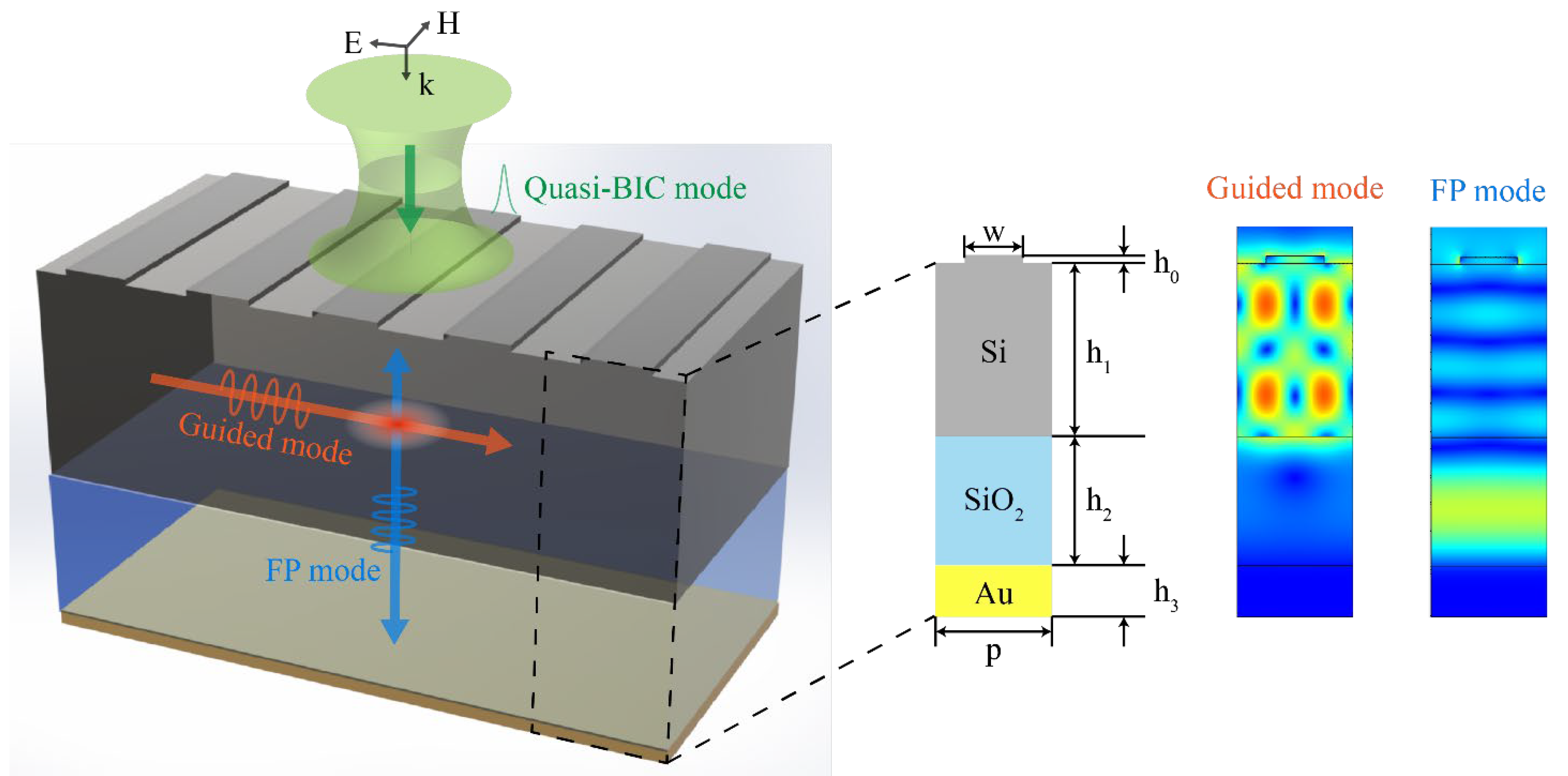
The quasi-BIC-based high-Q absorber in this work is composed of a Au substrate, a SiO2 spacer, and a Si layer from bottom to top, with gratings engraved on top of the Si layer (left panel in Figure 1). In this structure, BIC originated from the coupling between a guided mode and an FP mode. The guided mode horizontally propagates inside the Si layer (since the refractive index of Si is higher than that of SiO2), while the FP mode vertically oscillates between the Si and SiO2 layers (right panel in Figure 1). The Au substrate serves as a bottom mirror to prevent transmission and absorb the incident light. The SiO2 layer is used to separate the guided mode from the Au substrate to reduce the resistive loss. The resonance of the guided mode is determined by the period of gratings and the thickness of the Si layer, while that of the FP mode is determined by the thickness of both Si and SiO2 layers. Since the factors affecting the resonance of both modes slightly differ from each other, it is possible to tune one mode while maintaining the other. Thus, it is feasible to independently tune the resonant wavelength and the Q factor of the quasi-BIC mode. The cross-section of a single period is demonstrated in the middle panel of Figure 1, where w represents the width of the grating; p is the period; h0 is the grating thickness; h1 is the Si layer thickness; h2 is the SiO2 layer thickness, and h3 is the thickness of the Au substrate.
3.2. Characterization of the BIC Mode
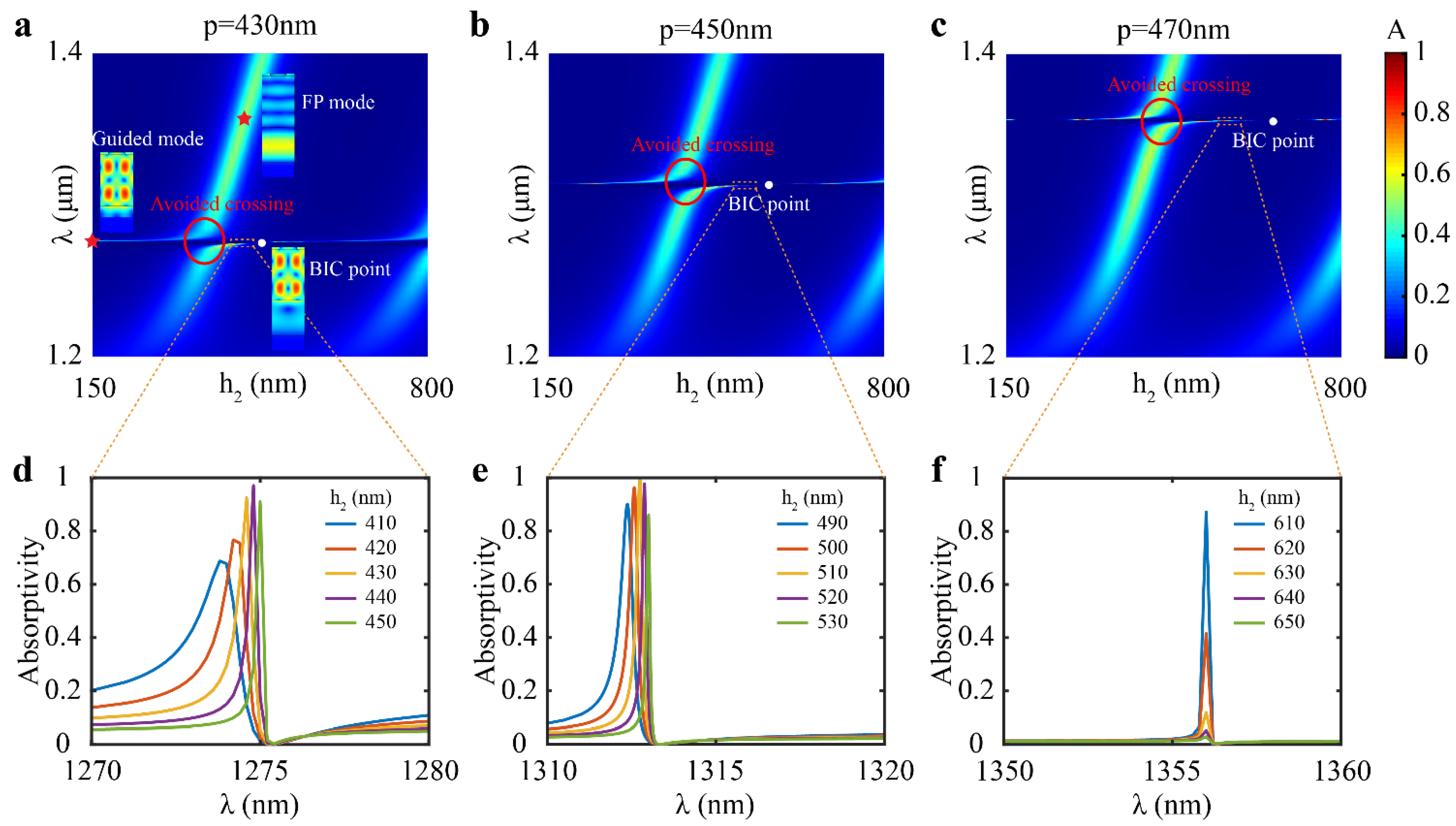
To study the characteristics of the BIC mode illustrated above, the dispersion relationship of absorptivity versus wavelength λ and the SiO2 layer thickness h2 was simulated for the structures with different periods p = 430 nm, 450 nm, and 470 nm (Figure 2a–c). Other structure parameters were set as h0 = 30 nm, h1 = 670 nm, h3 = 200 nm, and w = p/2. The track of the guided mode is parallel to the h2 axis, while that of the FP mode is almost an oblique straight line (Figure 2a–c). The resonance of the FP mode experiences a redshift with increasing h2, while the guided mode maintains the same resonant wavelength. On the other hand, the track of the FP mode maintains the same position, while that of the guided mode redshifts with increasing p. Thus, the resonances of the guided mode and the FP mode can be independently tuned by either changing p or h2.
The BIC point (white point in Figure 2a–c, where the peak absorptivity is zero) occurs in the vicinity of the avoided crossing (red circled area in Figure 2a–c). It is situated at the track of the guided mode and far from the track of the FP mode, and the quasi-BIC modes around the BIC point almost share the same resonant wavelength. The h2 values of each BIC point are about 480 nm, 560 nm, and 660 nm corresponding to p = 430 nm, 450 nm, and 470 nm, respectively. By comparing Figure 2a–c, it is noted that the resonant wavelength of the quasi-BIC mode is relevant to the period p and is hardly influenced by the thickness of SiO2 layer h2.
To study the influence of p and h2 on the quasi-BIC modes, five absorptivity curves (Figure 2d–f) were plotted for the quasi-BIC modes in the orange dashed areas of Figure 2a–c, with the interval of h2 as 10 nm. For all the periods, the difference between the resonant wavelengths is within 1 nm against the change of h2. Especially for p = 470 nm, the quasi-BIC modes resonate at the same wavelength of 1356 nm (Figure 2f), showing that the resonant wavelength is hardly influenced by h2. However, the resonant wavelength changes by nearly 40 nm when p changes by 20 nm. The resonant wavelengths are near 1275 nm, 1312 nm, and 1356 nm for p = 430 nm, 450 nm, and 470 nm, respectively (Figure 2d–f), indicating that the period is a key factor to change the resonant wavelength.
Besides the resonant wavelength, the Q factor (or the bandwidth) and the peak absorptivity of the quasi-BIC mode were also studied from Figure 2d–f. For p = 430 nm, the Q factor becomes higher (the bandwidth becomes narrower) when h2 is tuned from 410 nm to 450 nm (Figure 2d); for p = 470 nm, the peak absorptivity decreases when h2 is tuned from 610 nm to 650 nm (Figure 2f). These results suggest that h2 cannot be used to tune the resonant wavelength, but it can help to tune the Q factor (or the bandwidth) and the peak absorptivity.
These simulation results indicate that the resonant wavelength and the Q factor (the peak absorptivity) can be independently tuned in the quasi-BIC mode by changing either the period p or the SiO2 layer thickness h2.
3.3. Analysis of Q Factor and Peak Absorptivity
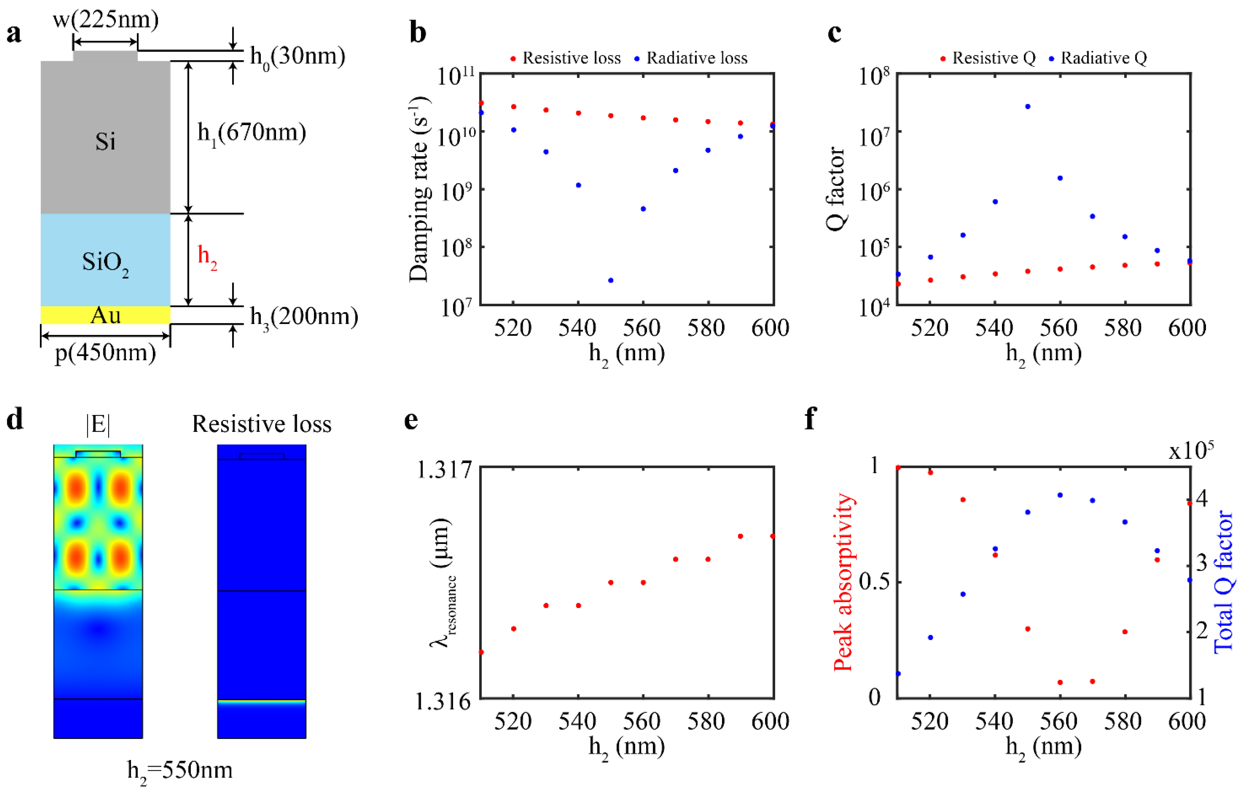
To further study the mechanism behind the Q factor and the peak absorptivity of the quasi-BIC mode, the energy damping rate was simulated by using the eigenfrequency method. Different parameters (p, h2, h0 + h1, etc.) influence the coupling between the guided mode and the FP mode in a similar way, i.e., by tuning the phase difference between these two modes. Since the period p was used to determine the resonant wavelength and the SiO2 layer thickness h2 was used to tune the coupling, h2 was set as the only variable in the following simulation, with other structure parameters as h0 = 30 nm, h1 = 670 nm, h3 = 200 nm, p = 450 nm, and w = 225 nm (Figure 3a). When h2 is changed from 510 nm to 600 nm (the BIC point is within this range), the damping rate of resistive loss maintains the magnitude of 1010 s−1, while that of radiative loss experiences a huge change from 107 s−1 to 1010 s−1 (Figure 3b). This indicates that h2 mainly influences the radiative loss and slightly influences the resistive loss. The change of resonant wavelength stays within 1 nm during the tuning of h2 (Figure 3e). For h2 = 550 nm (near the BIC point), the damping rate of resistive loss is nearly three orders higher than that of the radiative loss. According to the coupled mode theory [38], resistive and radiative losses serve key roles in tuning the Q factor and the peak absorptivity. Thus, the mechanism behind the Q factor and peak absorptivity tuning is that h2 can change the radiative loss.
The resistive Q factor and radiative Q factor can be transferred from the energy damping rate by using the formula (ω and γ represent the resonant angular frequency and the energy damping rate, respectively), as shown in Figure 3c. The total Q factor of the resonance can be obtained from (Qtot, Qres, and Qrad represent the total Q factor, resistive Q factor, and radiative Q factor, respectively). Thus, unlike dielectric BIC structures (without resistive loss), the total Q factor of the BIC mode in this work is limited by the resistive loss and cannot approach infinity. The resistive loss in this structure is mainly from the bottom Au substrate (Figure 3d). Moreover, the dissipation mainly happens within the top 50 nm of the Au substrate, which suggests that as long as the thickness of the Au substrate is larger than 50 nm, there will be no light transmission, and the absorption will be the same.
Comparing the simulation results of Figure 3b,f, it can be concluded that the closer the damping rates of resistive loss and radiative loss, the higher the peak absorptivity (i.e., closer to the condition of critical coupling). Unlike the total Q factor, the peak absorptivity decreases first and then increases during the change of h2 from 510 nm to 600 nm; i.e., the highest total Q factor corresponds to the lowest peak absorptivity. Thus, there is a tradeoff between the total Q factor and the peak absorptivity for this design of the quasi-BIC high-Q absorbers presented in this work.
3.4. Realizing Higher Q Factor While Maintaining High Peak Absorptivity
From the analysis above, high peak absorptivity of the quasi-BIC mode requires the damping rates of resistive loss and radiative loss to be as close as possible. Since the resistive loss is hardly influenced by the SiO2 layer thickness h2, one idea to simultaneously realize a higher Q factor and high peak absorptivity in the quasi-BIC mode is to decrease the damping rate of resistive loss at first and then tune that of radiative loss to the same magnitude as the resistive loss by changing h2. Thus, it is critical to find a way to lower the damping rate of resistive loss in the quasi-BIC mode.
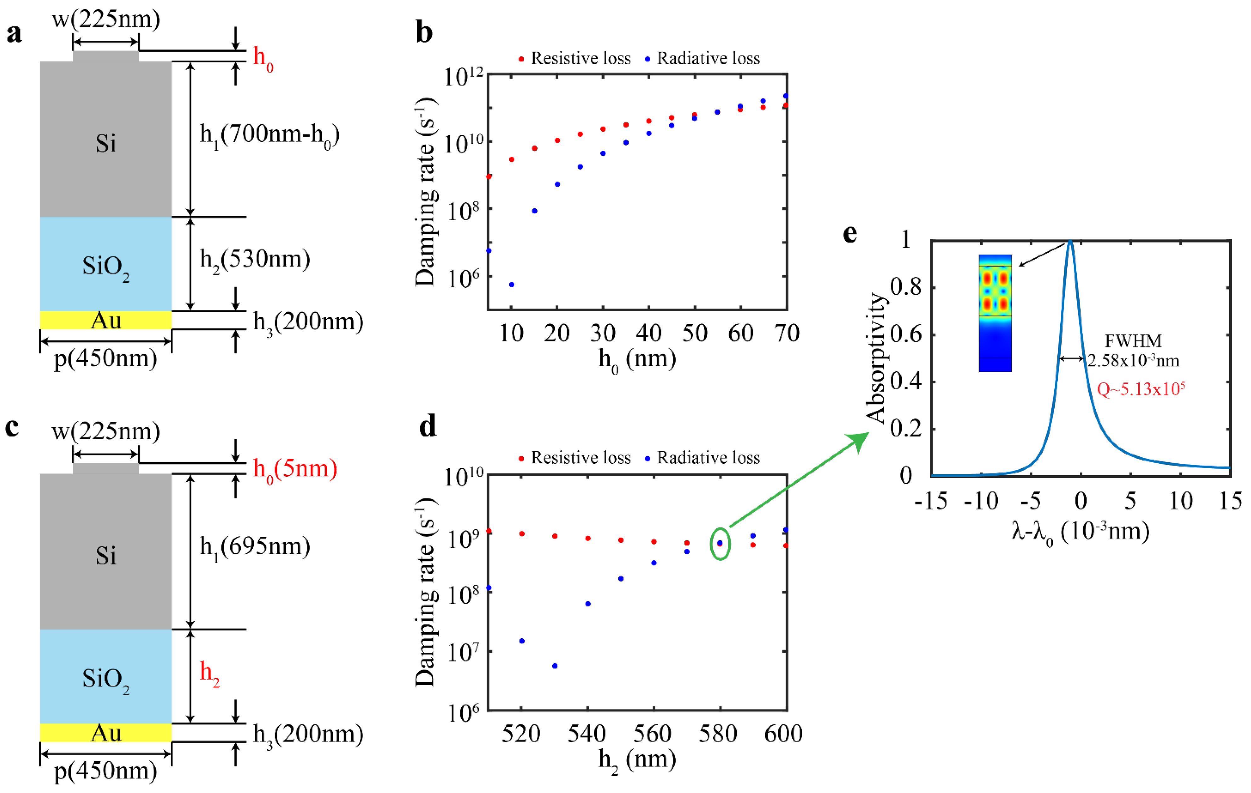
The grating thickness h0 is found to have the capability to change the damping rate of resistive loss. Simulations are conducted for the structure with parameters h0 + h1 = 700 nm, h2 = 530 nm, h3 = 200 nm, p = 450 nm, and w = 225 nm (Figure 4a). The damping rate of resistive loss increases by two orders—from 109 s−1 to 1011 s−1 when h0 is changed from 5 nm to 70 nm (Figure 4b). The damping rate of radiative loss decreases to 106 s−1 at first and then increases rapidly to 1011 s−1, suggesting that the resonance evolves to a BIC mode during the progress.
According to the design idea, h0 was set as 5 nm to decrease the damping rate of resistive loss as much as possible, and the next step was to tune the damping rate of radiative loss to the magnitude of resistive loss (Figure 4c,d). Setting h0 as 5 nm and keeping other structure parameters fixed, damping rates were simulated for different h2 values (from 510 nm to 600 nm). The damping rates of resistive loss and radiative loss almost equal to each other when h2 = 580 nm (green circled data in Figure 4d).
Finally, a quasi-BIC-based high-Q near-infrared perfect absorber was designed with the following structure parameters: h0 = 5 nm, h1 = 695 nm, h2 = 580 nm, h3 = 200 nm, p = 450 nm, and w = 225 nm. The absorptivity curve is shown in Figure 4e. The structure has a peak at 1323.375 nm (the electric field distribution is shown in the inset), and the peak absorptivity is unity. The FWHM (full width at half maximum) of the peak is as narrow as 2.58 × 10⁻³ nm, corresponding to a high Q factor of 5.13 × 10⁵.
3.5. General Steps to Design a Quasi-BIC-Based High-Q Perfect Absorber
Based on the structure in this work, a general idea to design a quasi-BIC-based high-Q absorber with high peak absorptivity can be formed. First, manipulate the resonant wavelength by tuning the period p; second, tailor the damping rate of resistive loss by tuning the grating thickness h0; last, make the damping rate of radiative loss approximately equal to that of resistive loss by tuning the SiO2 layer thickness h2.
4. Conclusions
We demonstrate a method to decouple the resonant wavelength and the Q factor in a quasi-BIC-based high-Q perfect absorber, and by using this method a near-infrared perfect absorber with Q factor as high as 5.13 × 10⁵ is designed. First, the design in this work is versatile such that it can be easily scaled to different operating wavelengths, e.g., mid-IR for sensing or high-Q emitter. Second, the mechanism of decoupling the resonant wavelength and the Q factor can used on other structures with two resonances that can be independently tuned. Third, by replacing the SiO2 layer with a dielectric elastomer actuator [39] (thickness could be varied dynamically), it could be possible to dynamically tune the Q factor while maintaining the resonant wavelength. Lastly, the structure proposed in this work can serve as a platform for cutting-edge technologies [40,41,42,43,44,45,46], including ultrasensitive biosensing [47], high-harmonic generations [48], and coherent and quantum light generations [49].
Author Contributions
W.Z. and Y.H. contributed equally to this work. Conceptualization, W.Z., Y.H., P.G. and Q.L.; methodology, W.Z. and Y.H.; software, W.Z. and Y.H.; validation, W.Z. and Y.H.; formal analysis, W.Z. and Y.H.; investigation, W.Z.; resources, W.Z.; data curation, Y.H.; writing—original draft preparation, Y.H.; writing—review and editing, P.G. and Q.L.; visualization, Y.H.; supervision, P.G. and Q.L.; project administration, Q.L.; funding acquisition, Q.L. All authors have read and agreed to the published version of the manuscript.
Funding
This work was supported by the National Natural Science Foundation of China (61975181).
Conflicts of Interest
The authors declare no conflict of interest.
References
- Singh, R.; Cao, W.; Al-Naib, I.; Cong, L.; Withayachumnankul, W.; Zhang, W. Ultrasensitive terahertz sensing with high-Q Fano resonances in metasurfaces. Appl. Phys. Lett. 2014, 105, 171101. [Google Scholar] [CrossRef] [Green Version]
- Ma, B.; Ouyang, A.; Zhong, J.; Belov, P.A.; Sinha, R.K.; Qian, W.; Ghosh, P.; Li, Q. All-Dielectric Metasurface for Sensing Microcystin-LR. Electronics 2021, 10, 1363. [Google Scholar] [CrossRef]
- Herr, T.; Brasch, V.; Jost, J.D.; Wang, C.Y.; Kondratiev, N.M.; Gorodetsky, M.L.; Kippenberg, T.J. Temporal solitons in optical microresonators. Nat. Photonics 2014, 8, 145–152. [Google Scholar] [CrossRef] [Green Version]
- Foley, J.M.; Young, S.M.; Phillips, J.D. Symmetry-protected mode coupling near normal incidence for narrow-band transmission filtering in a dielectric grating. Phys. Rev. B 2014, 89, 165111. [Google Scholar] [CrossRef]
- Li, P.B.; Gao, S.Y.; Li, F.L. Quantum-information transfer with nitrogen-vacancy centers coupled to a whispering-gallery microresonator. Phys. Rev. A 2011, 83, 054306. [Google Scholar] [CrossRef] [Green Version]
- Liu, Z.; Xu, Y.; Lin, Y.; Xiang, J.; Feng, T.; Cao, Q.; Li, J.; Lan, S.; Liu, J. High-Q quasibound states in the continuum for nonlinear metasurfaces. Phys. Rev. Lett. 2019, 123, 253901. [Google Scholar] [CrossRef] [Green Version]
- De Zoysa, M.; Asano, T.; Mochizuki, K.; Oskooi, A.; Inoue, T.; Noda, S. Conversion of broadband to narrowband thermal emission through energy recycling. Nat. Photonics 2012, 6, 535–539. [Google Scholar] [CrossRef]
- Wang, B.X.; Zhai, X.; Wang, G.Z.; Huang, W.Q.; Wang, L.L. A novel dual-band terahertz metamaterial absorber for a sensor application. J. Appl. Phys. 2015, 117, 014504. [Google Scholar] [CrossRef]
- Pan, M.; Su, Z.; Yu, Z.; Wu, P.; Jile, H.; Yi, Z.; Chen, Z. A narrowband perfect absorber with high Q-factor and its application in sensing in the visible region. Results Phys. 2020, 19, 103415. [Google Scholar] [CrossRef]
- Inoue, T.; De Zoysa, M.; Asano, T.; Noda, S. Single-peak narrow-bandwidth mid-infrared thermal emitters based on quantum wells and photonic crystals. Appl. Phys. Lett. 2013, 102, 191110. [Google Scholar] [CrossRef]
- Morita, R.; Inoue, T.; De Zoysa, M.; Ishizaki, K.; Noda, S. Photonic-crystal lasers with two-dimensionally arranged gain and loss sections for high-peak-power short-pulse operation. Nat. Photonics 2021, 15, 311–318. [Google Scholar] [CrossRef]
- Wang, B.; Yu, P.; Wang, W.; Zhang, X.; Kuo, H.C.; Xu, H.; Wang, Z.M. High-Q Plasmonic Resonances: Fundamentals and Applications. Adv. Opt. Mater. 2021, 9, 2001520. [Google Scholar] [CrossRef]
- Meng, L.; Zhao, D.; Ruan, Z.; Li, Q.; Yang, Y.; Qiu, M. Optimized grating as an ultra-narrow band absorber or plasmonic sensor. Opt. Lett. 2014, 39, 1137–1140. [Google Scholar] [CrossRef] [PubMed]
- Greffet, J.J.; Carminati, R.; Joulain, K.; Mulet, J.P.; Mainguy, S.; Chen, Y. Coherent emission of light by thermal sources. Nature 2002, 416, 61–64. [Google Scholar] [CrossRef] [PubMed]
- Zhao, D.; Meng, L.; Gong, H.; Chen, X.; Chen, Y.; Yan, M.; Li, Q.; Qiu, M. Ultra-narrow-band light dissipation by a stack of lamellar silver and alumina. Appl. Phys. Lett. 2014, 104, 221107. [Google Scholar] [CrossRef]
- Hsu, C.W.; Zhen, B.; Stone, A.D.; Joannopoulos, J.D.; Soljačić, M. Bound states in the continuum. Nat. Rev. Mater. 2016, 1, 16048. [Google Scholar] [CrossRef] [Green Version]
- Joseph, S.; Pandey, S.; Sarkar, S.; Joseph, J. Bound states in the continuum in resonant nanostructures: An overview of engineered materials for tailored applications. Nanophotonics 2021, 10, 4175–4207. [Google Scholar] [CrossRef]
- Gorkunov, M.V.; Antonov, A.A.; Kivshar, Y.S. Metasurfaces with maximum chirality empowered by bound states in the continuum. Phys. Rev. Lett. 2020, 125, 093903. [Google Scholar] [CrossRef]
- Koshelev, K.; Lepeshov, S.; Liu, M.; Bogdanov, A.; Kivshar, Y. Asymmetric metasurfaces with high-Q resonances governed by bound states in the continuum. Phys. Rev. Lett. 2018, 121, 193903. [Google Scholar] [CrossRef] [Green Version]
- Heilmann, R.; Salerno, G.; Cuerda, J.; Hakala, T.K.; Törmä, P. Quasi-BIC Mode Lasing in a Quadrumer Plasmonic Lattice. ACS Photonics 2022, 9, 224–232. [Google Scholar] [CrossRef]
- Azzam, S.I.; Shalaev, V.M.; Boltasseva, A.; Kildishev, A.V. Formation of bound states in the continuum in hybrid plasmonic-photonic systems. Phys. Rev. Lett. 2018, 121, 253901. [Google Scholar] [CrossRef] [PubMed] [Green Version]
- Yang, Y.; Peng, C.; Liang, Y.; Li, Z.; Noda, S. Analytical perspective for bound states in the continuum in photonic crystal slabs. Phys. Rev. Lett. 2014, 113, 037401. [Google Scholar] [CrossRef] [PubMed]
- Lee, S.G.; Kim, S.H.; Kee, C.S. Bound states in the continuum (BIC) accompanied by avoided crossings in leaky-mode photonic lattices. Nanophotonics 2020, 9, 4373–4380. [Google Scholar] [CrossRef]
- Gao, X.; Zhen, B.; Soljacic, M.; Chen, H.; Hsu, C.W. Bound states in the continuum in fiber Bragg gratings. ACS Photonics 2019, 6, 2996–3002. [Google Scholar] [CrossRef] [Green Version]
- Plotnik, Y.; Peleg, O.; Dreisow, F.; Heinrich, M.; Nolte, S.; Szameit, A.; Segev, M. Experimental observation of optical bound states in the continuum. Phys. Rev. Lett. 2011, 107, 183901. [Google Scholar] [CrossRef] [PubMed] [Green Version]
- Wan, S.; Qin, C.; Wang, K.; Wang, K.; Li, Y.; Guan, C.; Lv, B.; Li, W.; Shi, J. Ultra-high quality perfect absorber based on quasi bound states in the continuum. J. Appl. Phys. 2022, 131, 213104. [Google Scholar] [CrossRef]
- Hsu, C.W.; Zhen, B.; Lee, J.; Chua, S.L.; Johnson, S.G.; Joannopoulos, J.D.; Soljačić, M. Observation of trapped light within the radiation continuum. Nature 2013, 499, 188–191. [Google Scholar] [CrossRef] [Green Version]
- Friedrich, H.; Wintgen, D. Interfering resonances and bound states in the continuum. Phys. Rev. A 1985, 32, 3231. [Google Scholar] [CrossRef]
- Weimann, S.; Xu, Y.; Keil, R.; Miroshnichenko, A.E.; Tünnermann, A.; Nolte, S.; Sukhorukov, A.A.; Szameit, A.; Kivshar, Y.S. Compact surface Fano states embedded in the continuum of waveguide arrays. Phys. Rev. Lett. 2013, 111, 240403. [Google Scholar] [CrossRef]
- Bogdanov, A.A.; Koshelev, K.L.; Kapitanova, P.V.; Rybin, M.V.; Gladyshev, S.A.; Sadrieva, Z.F.; Samusev, K.B.; Kivshar, Y.S.; Limonov, M.F. Bound states in the continuum and Fano resonances in the strong mode coupling regime. Adv. Photonics 2019, 1, 016001. [Google Scholar] [CrossRef]
- Melik-Gaykazyan, E.; Koshelev, K.; Choi, J.H.; Kruk, S.S.; Bogdanov, A.; Park, H.G.; Kivshar, Y. From Fano to quasi-BIC resonances in individual dielectric nanoantennas. Nano Lett. 2021, 21, 1765–1771. [Google Scholar] [CrossRef]
- Wu, M.; Ha, S.T.; Shendre, S.; Durmusoglu, E.G.; Koh, W.K.; Abujetas, D.R.; Sánchez-Gil, J.A.; Paniagua-Domínguez, R.; Demir, H.V.; Kuznetsov, A.I. Room-temperature lasing in colloidal nanoplatelets via mie-resonant bound states in the continuum. Nano Lett. 2020, 20, 6005–6011. [Google Scholar] [CrossRef] [PubMed]
- Koshelev, K.; Bogdanov, A.; Kivshar, Y. Meta-optics and bound states in the continuum. Sci. Bull. 2019, 64, 836–842. [Google Scholar] [CrossRef] [Green Version]
- Abujetas, D.R.; Barreda, Á.; Moreno, F.; Litman, A.; Geffrin, J.M.; Sánchez-Gil, J.A. High-Q Transparency Band in All-Dielectric Metasurfaces Induced by a Quasi Bound State in the Continuum. Laser Photonics Rev. 2021, 15, 2000263. [Google Scholar] [CrossRef]
- Kim, K.H.; Kim, J.R. High-Q Chiroptical Resonances by Quasi-Bound States in the Continuum in Dielectric Metasurfaces with Simultaneously Broken In-Plane Inversion and Mirror Symmetries. Adv. Opt. Mater. 2021, 9, 2101162. [Google Scholar] [CrossRef]
- Liu, Z.; Wang, J.; Chen, B.; Wei, Y.; Liu, W.; Liu, J. Giant enhancement of continuous wave second harmonic generation from few-layer GaSe coupled to high-Q quasi bound states in the continuum. Nano Lett. 2021, 21, 7405–7410. [Google Scholar] [CrossRef] [PubMed]
- Hu, T.; Qin, Z.; Chen, H.; Chen, Z.; Xu, F.; Wang, Z. High-Q filtering and dynamic modulation in all-dielectric metasurfaces induced by quasi-BIC. Opt. Express 2022, 30, 18264–18272. [Google Scholar] [CrossRef]
- Haus, H.A.; Huang, W. Coupled-mode theory. Proc. IEEE 1991, 79, 1505–1518. [Google Scholar] [CrossRef] [Green Version]
- O’Halloran, A.; O’malley, F.; McHugh, P. A review on dielectric elastomer actuators, technology, applications, and challenges. J. Appl. Phys. 2008, 104, 071101. [Google Scholar] [CrossRef]
- Zhu, Y.; Luo, H.; Yang, C.; Qin, B.; Ghosh, P.; Kaur, S.; Shen, W.; Qiu, M.; Belov, P.; Li, Q. Color-preserving passive radiative cooling for an actively temperature-regulated enclosure. Light Sci. Appl. 2022, 11, 122. [Google Scholar] [CrossRef]
- Yu, J.; Ma, B.; Ouyang, A.; Ghosh, P.; Luo, H.; Pattanayak, A.; Kaur, S.; Qiu, M.; Belov, P.; Li, Q. Dielectric super-absorbing metasurfaces via PT symmetry breaking. Optica 2021, 8, 1290–1295. [Google Scholar] [CrossRef]
- Xu, Z.; Luo, H.; Zhu, H.; Hong, Y.; Shen, W.; Ding, J.; Kaur, S.; Ghosh, P.; Qiu, M.; Li, Q. Nonvolatile optically reconfigurable radiative metasurface with visible tunability for anticounterfeiting. Nano Lett. 2021, 21, 5269–5276. [Google Scholar] [CrossRef] [PubMed]
- Luo, H.; Zhu, Y.; Xu, Z.; Hong, Y.; Ghosh, P.; Kaur, S.; Wu, M.; Yang, C.; Qiu, M.; Li, Q. Outdoor personal thermal management with simultaneous electricity generation. Nano Lett. 2021, 21, 3879–3886. [Google Scholar] [CrossRef]
- Tian, J.; Li, Q.; Belov, P.A.; Sinha, R.K.; Qian, W.; Qiu, M. High-Q all-dielectric metasurface: Super and suppressed optical absorption. ACS Photonics 2020, 7, 1436. [Google Scholar] [CrossRef]
- Ying, Y.; Ma, B.; Yu, J.; Huang, Y.; Ghosh, P.; Shen, W.; Qiu, M.; Li, Q. Whole LWIR directional thermal emission based on ENZ thin films. Laser Photonics Rev. 2020, 2200018. [Google Scholar] [CrossRef]
- Xu, Z.; Li, Q.; Du, K.; Long, S.; Yang, Y.; Cao, X.; Luo, H.; Zhu, H.; Ghosh, P.; Shen, W.; et al. Spatially resolved dynamically reconfigurable multilevel control of thermal emission. Laser Photonics Rev. 2020, 14, 1900162. [Google Scholar] [CrossRef]
- Zito, G.; Sanità, G.; Alulema, B.G.; Yépez, S.N.L.; Lanzio, V.; Riminucci, F.; Cabrini, S.; Moccia, M.; Avitabile, C.; Lamberti, A.; et al. Label-free DNA biosensing by topological light confinement. Nanophotonics 2021, 10, 4279–4287. [Google Scholar] [CrossRef]
- Carletti, L.; Kruk, S.S.; Bogdanov, A.A.; De Angelis, C.; Kivshar, Y. High-harmonic generation at the nanoscale boosted by bound states in the continuum. Phys. Rev. Res. 2019, 1, 023016. [Google Scholar] [CrossRef] [Green Version]
- Azzam, S.I.; Kildishev, A.V. Photonic bound states in the continuum: From basics to applications. Adv. Opt. Mater. 2021, 9, 2001469. [Google Scholar] [CrossRef]
Figure 1.
Schematic of the quasi-BIC based high-Q perfect absorber (left panel), the cross-section of a single period (middle panel), and electric field distributions of the guided mode and the FP mode (right panel).
Figure 1.
Schematic of the quasi-BIC based high-Q perfect absorber (left panel), the cross-section of a single period (middle panel), and electric field distributions of the guided mode and the FP mode (right panel).

Figure 2.
Simulation results of absorptivity. (a–c) Dispersion relation of absorptivity versus wavelength and the SiO2 layer thickness for the period p values of 430 nm, 450 nm, and 470 nm, respectively. Insets show electric field distributions in (a) corresponding to the guided mode and the FP mode (the red stars) and the BIC point (the white point). Red circled area represents the avoided crossing. (d–f) The absorptivity curves for different SiO2 layer thicknesses h2 (with the interval of 10 nm), corresponding to the indicated orange dashed area of (a–c), respectively.

Figure 3.
Analysis of Q factor and peak absorptivity. (a) Schematic of the simulated structure. The only variable parameter is the SiO2 layer thickness h2. Plots of (b) damping rates and (c) Q factors versus h2. Red and blue dots represent resistive and radiative losses, respectively. (d) Distribution of electric field (left) and resistive loss (right) for h2 = 550 nm. (e) The resonant wavelength versus h2 plots. (f) Peak absorptivity (red dots) and total Q factor (blue dots) versus h2 plots. For all the above cases, h2 is tuned from 510 nm to 610 nm, with an interval of 10 nm.

Figure 4.
Design for increasing Q factor. (a) Schematic of the structure (grating thickness h0 is the variable parameter). (b) Damping rates versus h0 plots. Red and blue dots represent resistive and radiative losses, respectively. Grating thickness h0 is varied from 5 nm to 70 nm, with an interval of 5 nm. (c) Schematic of the structure (h0 is set as 5 nm, and the SiO2 layer thickness h2 is varied). (d) Damping rates versus h2 plots. SiO2 layer thickness h2 is changed from 510 nm to 600 nm, with an interval of 10 nm. (e) Absorptivity curve for the green circled structure parameter in (d). Inset represents the electric field distribution at the peak, λ0 = 1323.375 nm.

Publisher’s Note: MDPI stays neutral with regard to jurisdictional claims in published maps and institutional affiliations. |
© 2022 by the authors. Licensee MDPI, Basel, Switzerland. This article is an open access article distributed under the terms and conditions of the Creative Commons Attribution (CC BY) license (https://creativecommons.org/licenses/by/4.0/).
Share and Cite
MDPI and ACS Style
Zha, W.; Huang, Y.; Ghosh, P.; Li, Q. Quasi-BIC-Based High-Q Perfect Absorber with Decoupled Resonant Wavelength and Q Factor. Electronics 2022, 11, 2313. https://doi.org/10.3390/electronics11152313
AMA Style
Zha W, Huang Y, Ghosh P, Li Q. Quasi-BIC-Based High-Q Perfect Absorber with Decoupled Resonant Wavelength and Q Factor. Electronics. 2022; 11(15):2313. https://doi.org/10.3390/electronics11152313
Chicago/Turabian StyleZha, Weiyi, Yun Huang, Pintu Ghosh, and Qiang Li. 2022. "Quasi-BIC-Based High-Q Perfect Absorber with Decoupled Resonant Wavelength and Q Factor" Electronics 11, no. 15: 2313. https://doi.org/10.3390/electronics11152313
Note that from the first issue of 2016, this journal uses article numbers instead of page numbers. See further details here.