1. Introduction
The time gating of single-photon avalanche diodes (SPADs) was commonly used as a method to reduce the dark count rate (DCR) and afterpulsing in biomedical imaging applications such as diffuse optical tomography (DOT) [
1], fluorescence lifetime imaging microscopy (FLIM) [
2], and Raman spectroscopy [
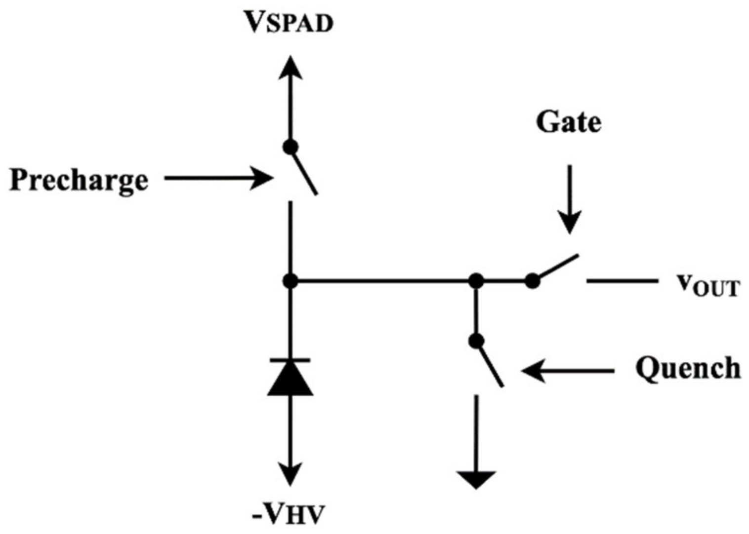
3] because the photon arrivals in these applications are correlated with a reference clock. Time-gated SPAD pixels, illustrated conceptually in
Figure 1, work by pre-charging the SPAD above their breakdown voltage just before closing the gate to enable their output.
At the end of the window, the gate is opened to disable the output, and the SPAD bias is quickly reduced below breakdown by a parallel quenching switch. As the approximate arrival time of photon absorption is known, the SPAD can be enabled only during a specified time window where the anticipated photon events are most likely to occur in order to improve the signal-to-noise ratio (SNR). While time gating was primarily adopted to reduce the effects of noise, it can also be used to obtain the timing information of the photon events by shifting the gate window with respect to a synchronous laser pulse to create histograms of the SPAD counts.
In [
4], an array containing 8192 SPADs utilized a combination of on-chip and off-chip delay lines to shift a single gate window of the SPAD array in 250 ps increments over a range of 32 ns. By measuring the SPAD outputs for a large number of cycles in each gate delay setting, a histogram with 250 ps time bins was constructed by subtracting SPAD counts from adjacent gate delay settings. More recently, a similar approach demonstrated gate shifting capabilities as fine as 18 ps when a clock generation block was implemented in a field programmable gate array (FPGA) [
2]. The main disadvantage of these approaches is that histograms need to be constructed sequentially in each gate delay setting, reducing the frame rate. In [
5], four time-gates of different widths, but starting at the same instant in time, were applied to a SPAD array using an off-chip delay generator. This approach allows for simultaneous acquisition of the data for different gate windows, thus reducing the time needed to produce a valid histogram. Acquisition speed and high photon detection efficiency (PDE) are key considerations in an application such as DOT, where fast and high-fidelity images are required to avoid motion artifacts or tissue variations during the measurement, even with a low number of photons. However, current research works have either sequentially shifted the gate windows of an array of SPADs, which increases the measurement time or have not yet fully-integrated the multi-gate generation into the same chip as the SPAD, which reduces the effective PDE.
In this paper, we designed and performed detailed measurements of a 4 × 4 multi-time-gated SPAD array in the TSMC 65 nm standard CMOS process. Here, shifted gate windows are applied to each column of SPADs, so each column covers a different portion of the timing range. As such, the time for DOT measurements could potentially be reduced since the separate gate windows are applied simultaneously. However, compared to the traditional time-gated operation in which all SPADs work simultaneously in the time-gated windows [
6,
7], only a certain portion of SPADs is active in the specific time-gated windows, thus having a negative impact on the effective PDE. It is worth noting that there is a trade-off between the measurement efficiency and SNR using multi-time-gated SPAD operations.
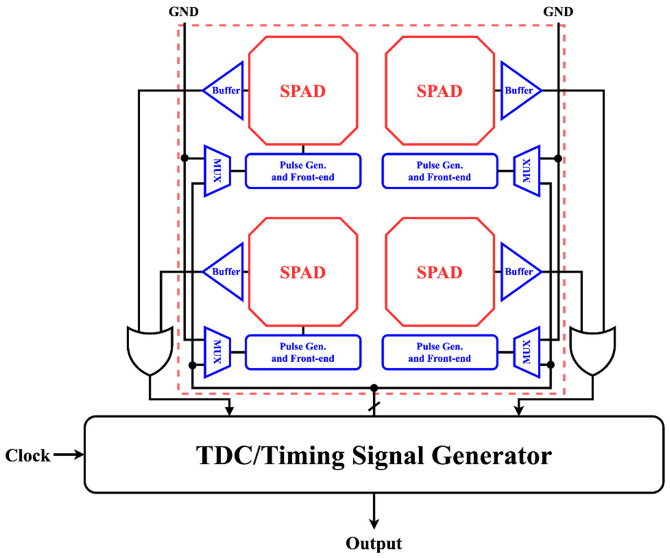
A conceptual diagram of the proposed multi-time-gated SPAD array is shown in
Figure 2. The input clock to the circuit is synchronous with a pulsed laser. Delayed rising edges of the clock are tapped from a multi-purpose delay line, which provides shifted gate windows that are overlapped by approximately half the gate width to each column of SPADs (see details in
Section 2.2). Therefore, each SPAD column is responsible for constructing a small section of the histogram, which can later be combined to give the final result. This allows for the use of narrow gate windows to improve the SNR of the SPADs, while still maintaining a large timing dynamic range. The time to construct a full histogram can also be reduced compared to shifting a single gate window across the array, since the multiple time gates are applied simultaneously to obtain the histogram in multiple time gate windows at the same time. The gate window generation circuit for this design is also fully integrated on the same chip as the SPADs in the form of a multi-purpose delay line which serves three purposes: shifting the gate windows of adjacent SPAD columns; generating the time-gating pulses for the SPAD pixels; and performing coarse time-to-digital conversion. Each time-to-digital converter (TDC) channel is shared by the SPADs within the same column through an OR gate, such that the first SPAD in a column to turn on in a given cycle will be time stamped. Due to the shared circuitry, this design can be fully integrated with the SPAD array while minimizing the impact on the array’s fill factor.
As a proof of concept, a 4 × 4 SPAD array was designed in the TSMC 65 nm standard CMOS process using this structure. The proposed design structure has the following advantages compared to the traditional single time-gated structures. First, this design could serve as a repeated structure to create a larger array due to the scalability of this design as a result of using shared circuitry. Second, the proposed multi-purpose delay line allows the SPAD array to operate in time-gated modes with shifted gate windows. Therefore, it can measure the time-correlated information in multiple time windows to cover a large time range simultaneously, thus reducing the time and complexity to obtain the full measurement range for time-correlated single photon-counting applications. Third, the proposed multi-purpose delay line can also function as a shifted gate generator and a coarse TDC, thus resulting in a very compact layout design and eventually an increased fill factor for the SPAD array. Fourth, this proposed structure is designed and fabricated in a standard 65 nm CMOS technology. As a result, it has a low fabrication cost and can be easily tiled to form a large-scale array that shares a single fine-interpolation TDC to achieve higher timing resolution and lower timing jitter on photon events. The prototype chip achieves a median DCR of 37 kHz, 4.37 ns gate widths, 550 ps timing resolution, and a peak photon detection probability (PDP) of 42.9% at 420 nm, all at a 0.8 V excess bias.
The remainder of this paper is organized as follows. In
Section 2, we discuss the circuit design of the multi-time-gated SPAD array. Next, in
Section 3, we describe the measurement procedures and discuss the results. Finally, in
Section 4, we provide the conclusions.
2. Circuit Design
In this section, we present an overview of the design by first discussing the individual time-gated SPAD pixel design and then explaining how the design was expanded to obtain the multi-time-gated operation. Afterwards, the layout is shown at the end of the section with a sample of post-layout transient simulation results.
2.1. SPAD Pixel Design
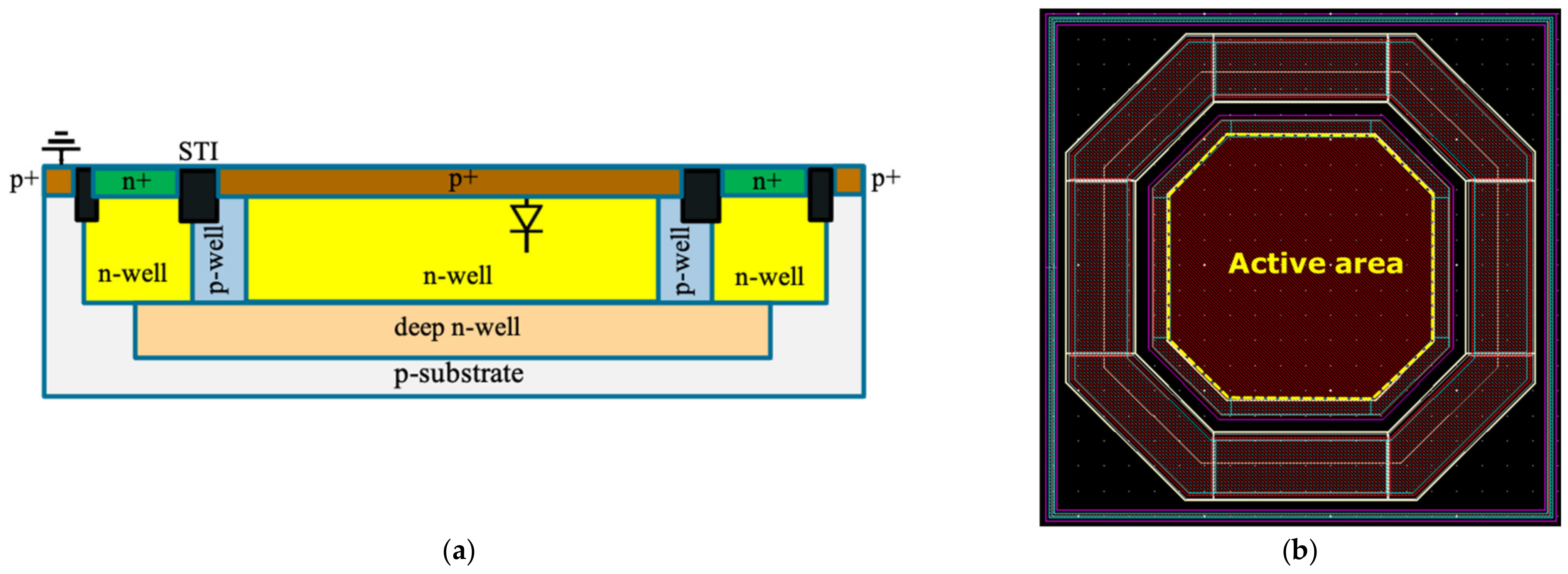
A p+/n-well SPAD was used in the multi-time-gated array. The illustration of the cross-sectional view and top view in Cadence Virtuoso are shown in
Figure 3a,b, respectively. The SPAD was designed conservatively to ensure correct functionality in a single design iteration. It consists of a ~10 μm diameter active area and achieves a fill factor of ~24.5%. A silicide-blocking layer was placed over the active area, with an opening only above the active area to ensure that incident photons are more likely to be absorbed in the active area of the SPAD.
An octagonal shape was used for the SPAD active area as obtuse corners within the SPAD structure were shown to reduce premature edge breakdown (PEB) compared to using sharp 90-degree corners [
8]. An additional method of reducing PEB is by using a p-well guard ring [
9]. As the p+ region extends beyond the n-well and into the p-well, the lower doping of the p-well reduces the electric field strength near the edges. This ensures the strongest field in the planar junction of the SPAD. The p+ region extending beyond the n-well had the added benefit of pushing the shallow trench isolation (STI) away from the active area, mitigating the effect of STI-generated carriers initiating avalanches, thus improving the dark noise performance of the SPAD [
10,
11].
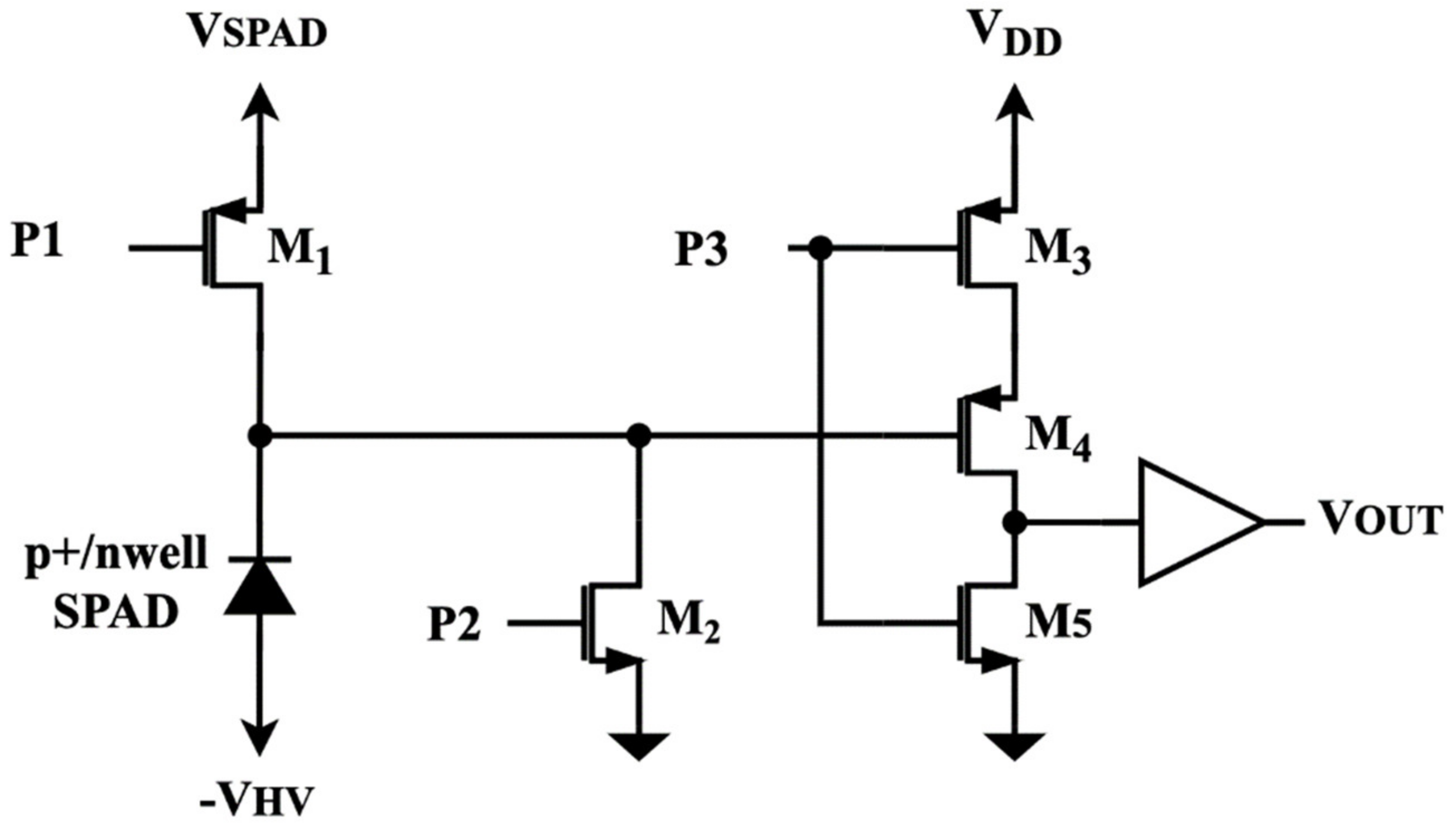
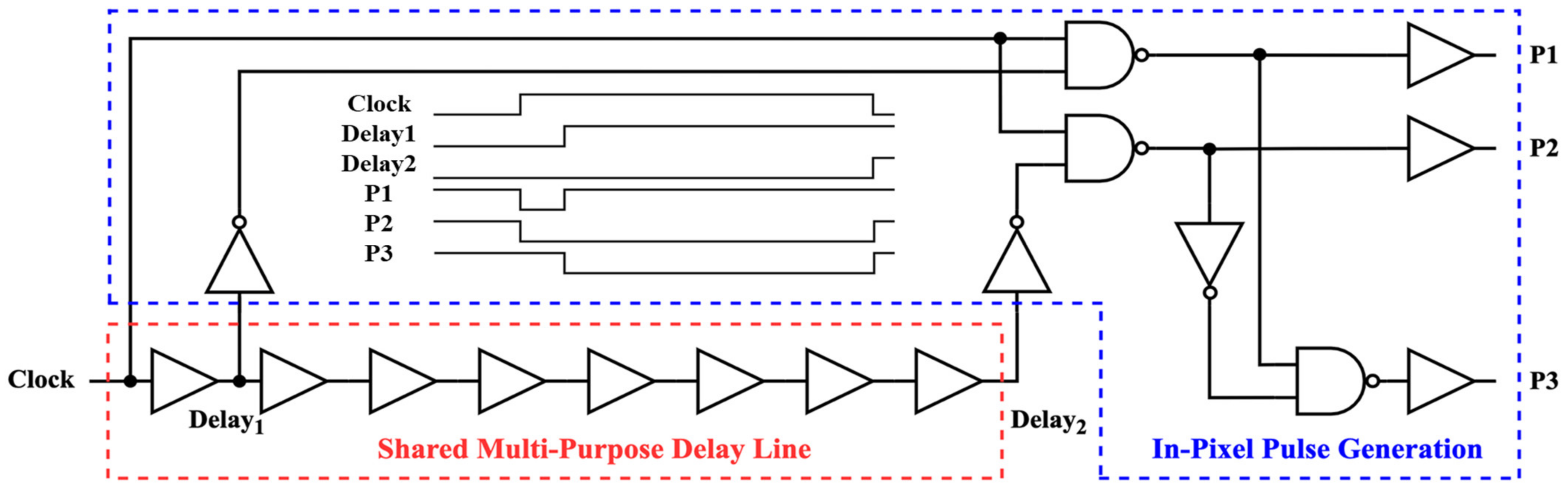
To obtain the gating operation, the SPAD front-end circuitry was designed as shown in
Figure 4 with the active-low P1 and P3 pulses and the active-high P2 pulse being generated by the circuit shown in
Figure 5. This front-end circuit is based on previous designs from our group [
12,
13]. A negative high voltage is applied to the anode of the SPAD. In the initial state, P2 is high to ensure that the SPAD’s cathode is discharged to ground, and the SPAD is biased below its breakdown voltage. A short P1 pulse (i.e., a few hundred picoseconds) then turns on M1 at the same time that P2 turns off M2, which charges the SPAD cathode to V
SPAD. The SPAD’s bias is then above its breakdown voltage. At the end of the P1 pulse, the P3 pulse transitions and enables the output branch of the SPAD front-end. Thus, when a photon triggers an avalanche in the SPAD, the gate of M4 will be discharged below its switching point, forming a low-resistance path to V
DD through M3 and M4 to generate the output pulse.
In our previous designs, the P1, P2, and P3 pulses were generated using buffers with large capacitive loads to create the required delays [
12]. In this design, we use a tapped delay line to create the delays, such that taps from a single delay line can be used for three functions: (1) Generate the gating pulses P1, P2, and P3 for each SPAD pixel in the array. (2) Perform shifting of the gate windows for adjacent pixels. (3) Accomplish the coarse time-to-digital conversion. The delay line is shared by each pixel of the design and will be discussed in detail in the next subsection, while the pulse generation logic is integrated directly within each pixel. Conceptually, the rising edge of the clock signal can be used to denote the start of the P1 and P2 pulses, and the next tap of the delay line can quickly disable the P1 pulse, such that pre-charging of the SPAD occurs very quickly. After a number of buffers required to achieve the desired gate width, another tap of the delay line can then be passed to the in-pixel pulse generation circuit to bring P2 to the high level to end the gate window. The output controlling pulse P3 is generated using P1 and P2 through an inverter and a NAND as shown in
Figure 5.
In our current design, the individual SPAD pixel achieved a fill factor of ~18% compared to the ~24.5% fill factor of the SPAD itself. This fill factor can be improved mainly by optimizing the SPAD layout, as there is more area to be saved in the SPAD structure than in the optimization of the size of the front-end circuits.
2.2. Multi-Time-Gated Array Design
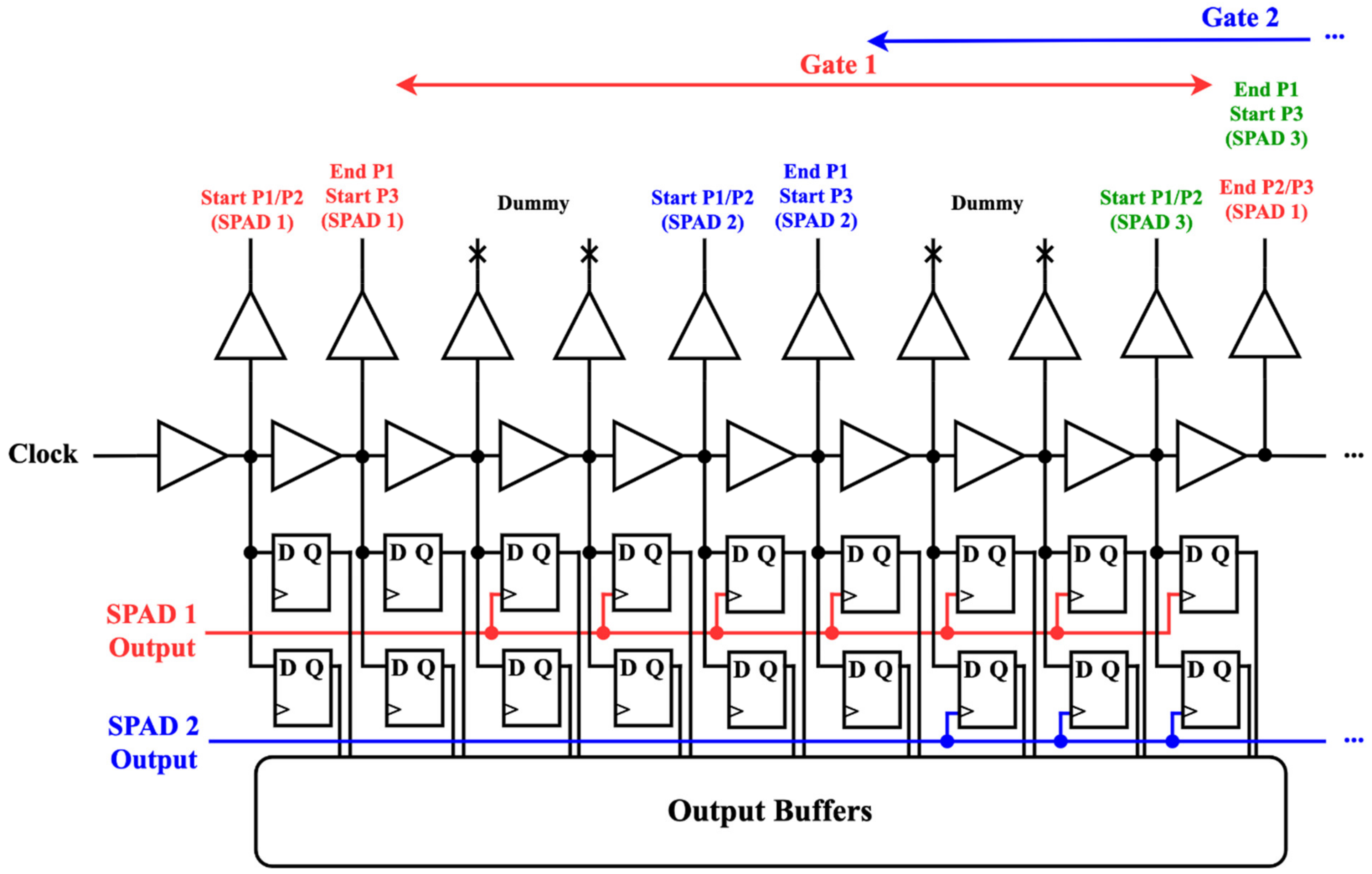
For the multi-time-gated delay, we need to generate the P1, P2, and P3 pulses using delayed replicas of the input clock, which are also used to shift the gate windows of adjacent SPADs and perform coarse time stamping of photon arrivals. Therefore, we implemented a single multi-purpose delay line to simultaneously accomplish all these functions. By sharing the circuitry in this manner, the impact on the array’s fill factor can be minimized. The general structure of the multi-purpose delay line is shown in
Figure 6. An external clock signal is applied as the input for the first buffer of the delay line, which initiates the gating pulse generation for the first pixel. At the same time, the clock’s rising edge propagates through the series of buffers toward the delay taps associated with the next SPAD pixels. To overlap the gate windows of SPADs in adjacent columns by half of the gate width, the delay taps used to generate the P1, P2, and P3 of the next column will start from a delay tap occurring halfway through the previous gate window. When a SPAD generates an output pulse, it will clock the D flip-flops (DFFs) whose data inputs are connected to the delay line taps within its respective gate window.
A primary consideration when designing the delay line is to maintain equal capacitive loads for each delay buffer to reduce delay mismatches that contribute to nonlinearity in the timing performance. For this reason, each tap of the delay line is not directly connected to the pulse generation logic of the corresponding SPAD column. Instead, the tapped delay is first passed through an intermediate buffer, such that the load on the actual delay cells is consistent regardless of the connections to the SPAD front-end. A similar approach is used on the DFFs that sample the delay line state for the coarse time-to-digital conversion. As the gate windows overlap by half of the gate width, most delay line taps need two DFFs to be clocked by two neighboring SPAD columns. Dummy DFFs are used to ensure the same capacitive load at each stage, even when they are not clocked by a SPAD output. This case mainly happens at the start and end of the multi-time-gated array, where only a single SPAD column will cover that portion of the timing range. Another important consideration is the influence from the operating temperature. To investigate this issue, we performed simulations with different temperatures to see the variations of the time-gated windows. The simulations showed that the time-gated windows were 2.84 ns for 7 °C, 2.96 ns for 27 °C, 3.08 ns for 47 °C, and 3.20 ns for 67 °C, respectively. These results clearly showed the temperature dependence of the pulse generation circuit. We also performed the simulation of the power consumption for the proposed 4 × 4 SPAD array, which presented an averaged power consumption of 76.5 µW with a 20 MHz clock. The temperature effect will become more severe in a large SPAD array since it requires a higher power consumption. Therefore, the temperature may increase significantly due to the self-heating effect on the chip. One possible solution is to control the operating temperature for the SPADs, which increases the cost and the complexity of the integration for the SPAD application systems. Another further improved implementation can use a delay locked loop (DLL) to lock the delay line to a reference, thus ensuring consistent performance across PVT variations and minimizing the jitter of the delay line [
14,
15].
The final output of the circuit consists of four bits for each SPAD column that are buffered to the chip output through DFFs. The first bit is a status signal that indicates if a SPAD pulse occurred during the given time-gated period. This signal is generated from a DFF with the data input tied high and the associated SPAD column serving as the clock input. The remaining three bits for the output of a given column come from the three-bit output code of the coarse TDC. The DFFs are then reset after the falling edge of the clock when the measurement interval is complete. Since in DOT experiments the event rate is kept low to avoid pile-up, a single fine-interpolating TDC could be shared in future by an array of the proposed design while missing a minimal number of events. This second-stage TDC would increase the resolution by quantizing the remainder of the coarse time-to-digital conversion to generate additional fine time resolution bits.
In the layout of the multi-purpose delay line, matching between the traces in the array is a key consideration. The delay line was designed such that the spacing of the buffers was evenly distributed along the bottom of the array of SPADs. Variations in routing are also a factor that contribute to the timing nonlinearity, as they impact the capacitive load seen by each stage. By designing the spacing of buffers to match the pitch of SPAD pixels within the array, the trace lengths can be more closely matched to avoid larger variations in the capacitance that degrade the timing performance. The multi-purpose delay line circuit occupies an area of 0.001 mm2 for the multi-time-gated array design.
In this design, an additional feature that each SPAD pixel could be disabled by externally configurable mask bits was included. This allows for disabling “hot-pixels” that have a much higher DCR than the majority of the pixels within the array. For the purposes of testing, it allows us to easily assess the performance of each individual SPAD. The mask bits control the select input of MUXs that are placed within each SPAD pixel. The MUXs will either connect the taps from the multi-purpose delay line that initiate the gating pulses to the SPAD front-end or tie the P1, P2, and P3 inputs of the SPAD front-end circuit to GND such that the SPAD is disabled.
2.3. Post-Layout Simulation
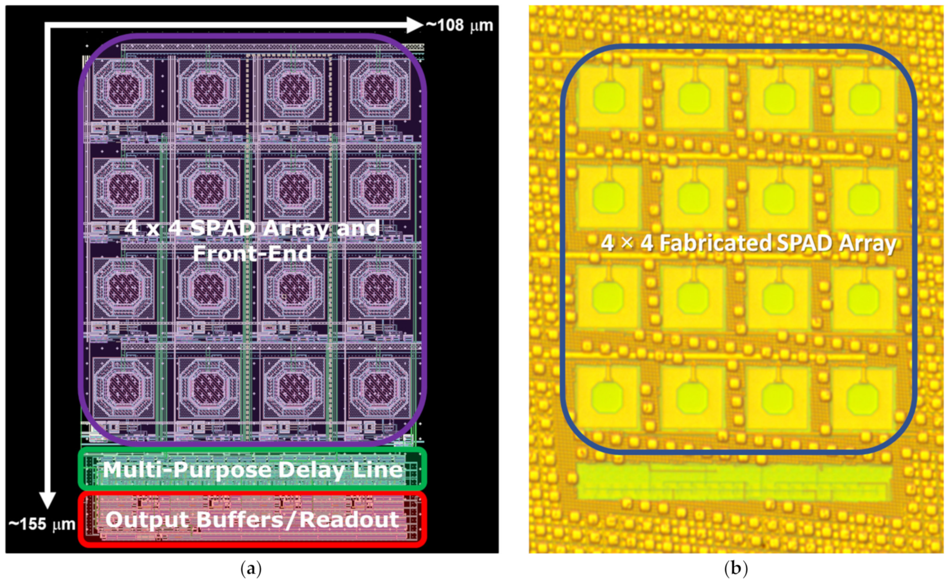
The final layout and the micrograph of the fabricated circuit of the multi-time-gated SPAD array are shown in
Figure 7a,b, respectively. In this array, the four SPADs within a column are ORed together. Therefore, they can share the same channel of the multi-purpose delay line and readout circuitry, resulting in an improved fill-factor of the array. The limitation here is that the counts from different SPADs within the same column are indistinguishable from each other due to the spatial compression when ORing their outputs. The final design occupies a total area of 0.017 mm
2 for an array’s fill factor of ~9.6%, including the output buffers. The SPAD pixels themselves largely limit the array’s fill factor due to the conservative design choices made to ensure a correct functionality on the first fabrication attempt. For an improved design, the SPAD pixel’s fill factor could be optimized, and approaches such as well sharing or guard ring sharing could be used to minimize the pitch between adjacent SPADs [
16].
Based on the layout in
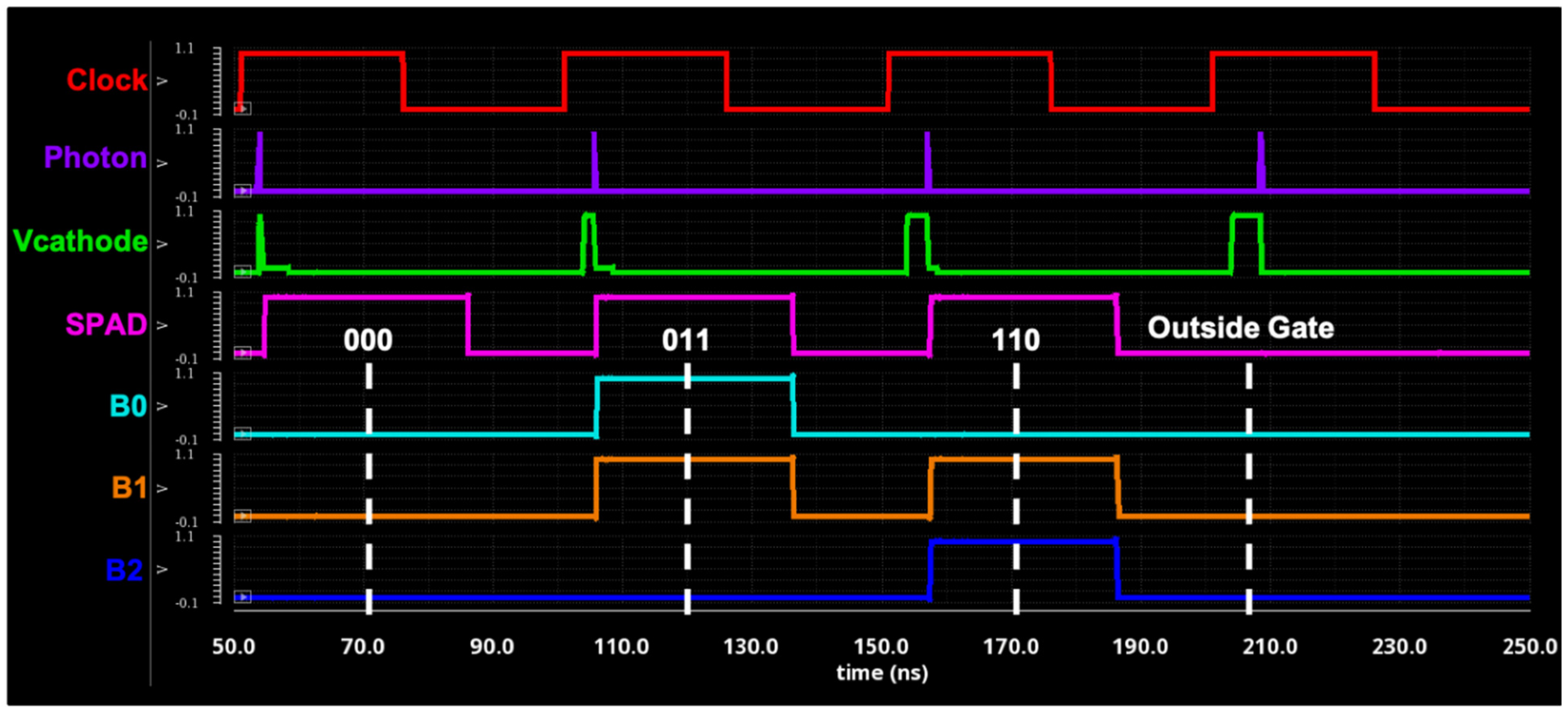
Figure 7a, a post-layout simulation was performed to demonstrate the design functionality. As shown in
Figure 8, the “Clock” represents a 20-MHz clock that was applied at the input of the SPAD array, “Photon” is a signal that simulates the arrival of a detectable photon, “V
cathod” is the SPADs’ cathode voltage, “SPAD” is the ORed SPAD output pulse, and B
2B
1B
0 are the codes sampled from the coarse TDC when a photon is detected in a gate window. A simulation model for the SPAD was used according to [
17], and the photon arrival time was increased with respect to the clock by 1.5 ns in each cycle to validate the functionality across the sensor’s dynamic range.
It can be seen from
Figure 8 that after a delay from the rising edge of the clock, the SPAD pixel’s cathode voltage is pre-charged by its front-end circuitry to arm the SPAD for photodetection. In the first clock cycle, the photon arrives at the very start of the gate window, causing the cathode voltage to discharge and the SPAD to generate an output pulse. The resulting TDC code (i.e., read as B
2B
1B
0) is 000, as the photon arrives at the very start of the gate window opening, and the clock’s rising edge has propagated a minimal distance through the delay line. As the photon is simulated to arrive 1.5 ns later in each cycle, the TDC code gradually increases from 000 to 011 and 110. However, when the arrival of a photon is outside the gate window (the fourth cycle in
Figure 8), the SPADs have no response, thus do not generate a TDC code. Note that the displayed output waveforms are buffered through DFFs that are reset after a delay of the falling edge of the clock. This design choice was made for easier testing of the chip, as the falling edge of the clock could be used as a trigger for sampling the result during a measurement cycle.
3. Results and Discussions
In this section, we present and discuss the measurement process and the achieved results for the proposed multi-time-gated SPAD array.
3.1. Breakdown Voltage
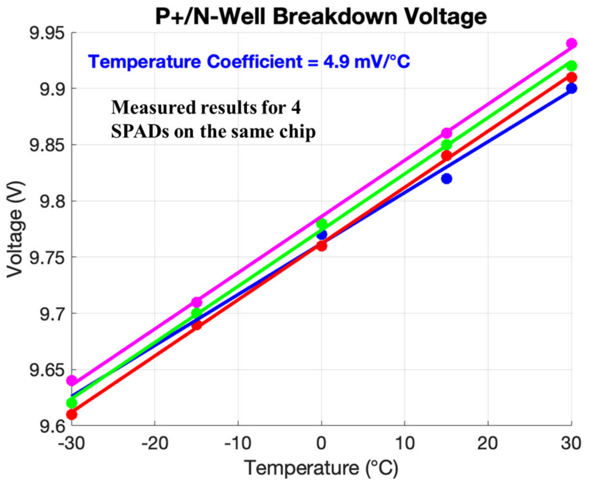
To measure the breakdown voltage of the SPAD, the test PCB was placed inside an Espec thermal chamber and connected to an external Agilent B1500A semiconductor device analyzer. The semiconductor device analyzer was used to apply a bias voltage to the SPAD which increased in small steps and to measure the DC current, generating a current-voltage (I–V) curve for the SPAD. Then, the breakdown voltage can be extracted through the I–V curve, which corresponds to the voltage point of the curve where the maximum derivative occurs. As shown in
Figure 7b, there is no accessible pad to measure the breakdown voltage for the individual SPAD in the 4 × 4 array. Therefore, the measurement was performed on four separate standalone SPADs with the same structure fabricated on the same chip using the same process. Their breakdown voltages were measured at temperatures ranging from −30 °C to +30 °C in 15 °C increments. For each point on the graph, 10 measurements of the IV characteristics were averaged to avoid the impact of any variation during the measurement.
Room temperature within our lab setting was ~25 °C, at which the average breakdown voltage for these 4 SPADs was measured to be 9.88 V with a small standard deviation of 17 mV. This indicates that the variations of the fabrication process are very small. The results of the breakdown voltage measurement versus temperature are presented in
Figure 9. By performing a best linear fit to the data points for each of the four SPADs, the average slope was taken as the temperature coefficient of 4.9 mV/°C. The remaining measurements on the time-gated SPAD were taken using an excess voltage of 0.8 V. This is slightly below the maximum excess voltage for the pixel of 1 V to keep the gate voltages on the MOSFETs of the front-end circuits within the limited gate voltage (1 V) for this standard 65 nm CMOS technology considering the possibility for the variations in the breakdown voltage across the array.
3.2. Time-Gated Windows
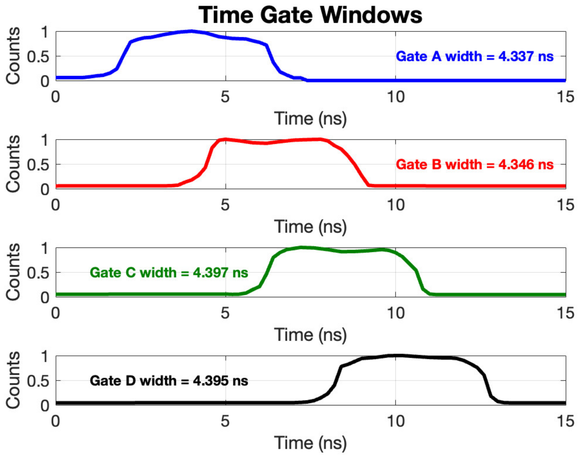
To measure the gate windows of the SPAD columns, the SPAD bias and supply voltages for the chip core and IO ring were supplied from an Agilent E3646A DC power supply. The gate clock with a 1 MHz repetition rate was generated by the first channel of a Berkeley Nucleonics Model 745 digital delay generator. To vary the arrival time of the photons within the gate window, the second channel of the delay generator sent delayed replicas of the clock, in 200 ps steps to a PicoQuant PDL 800-B laser driver connected to an LDH-P-C-690 laser head with a center wavelength of 685 nm. To avoid pile-up distortion in the measurements, the optical power was adjusted such that the total pixel counts were less than 1% of the repetition rate of the laser driver. Additionally, it was verified that the total counts from photons were more than 10 times larger than the DCR to reduce the influence of the dark counts on the timing measurement results. The counts were recorded with a Lecroy Waverunner 625Zi oscilloscope for 10 million gate windows per delay setting to build a histogram. The average of the histogram was the number of the counts for each delay setting. The number of counts of all points were recorded and then normalized through dividing by the maximum number of the counts for each point to generate the time gate windows shown in
Figure 10.
As shown in
Figure 10, the multi-time-gated operation is verified, as adjacent gate windows overlap by half the gate width. The values of the gate windows were very consistent, being 4.37 ns with a small standard deviation of ~30 ps. This also indicates a small process variation during the fabrication and a good matching in the layout design. Additionally, this array demonstrated fast 20–80% gate rise and fall times of ~520 ps and 620 ps, respectively, which were derived from using linear interpolation on the measured time-gate windows.
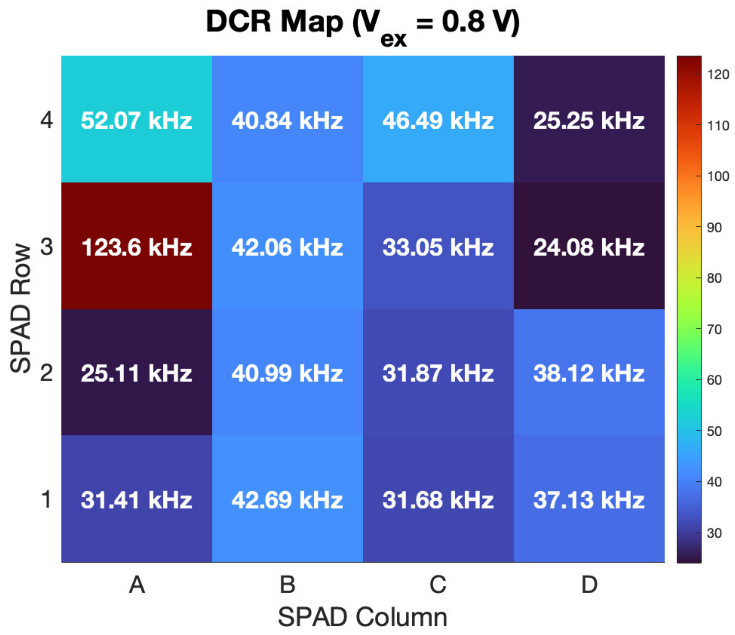
3.3. Dark Count Rate
To measure the dark noise of the SPAD in a time-gated configuration, the dark count probability (DCP) was measured as opposed to the dark count rate (DCR). The DCP of a time-gated SPAD indicates the probability of a pulse to be measured during a gate window with no incident light on the SPAD. The effective DCR can then be obtained by normalizing the DCP to the width of the gate window. For this measurement, the SPAD bias, and supply voltages for the chip core and IO ring were provided by an Agilent E3646A DC power supply, and the SPAD outputs were counted by a Lecroy Waverunner 625Zi oscilloscope. A 1 MHZ clock for the gate windows was generated from a Berkeley Nucleonics Model 745 digital delay generator. The oscilloscope collected counts from the time-gated array at room temperature until the exponential tails of the interarrival time histograms had become stable.
Figure 11 shows the DCR map for the multi-time-gated array when the excess bias is 0.8 V. The median DCR of the array was determined to be ~37 kHz (i.e., pixel D1). This level of DCR is reasonable for SPADs designed in standard CMOS processes [
18,
19,
20]. From
Figure 11, it can also be seen that the measured array demonstrated one “hot-pixel” whose noise (123.6 kHz) is notably higher than the rest of the array (i.e., pixel A3). This demonstrated the usefulness of including MUXs in the proposed design to disable individual pixels, as it is common to have some erroneous pixels when designing arrays of SPADs.
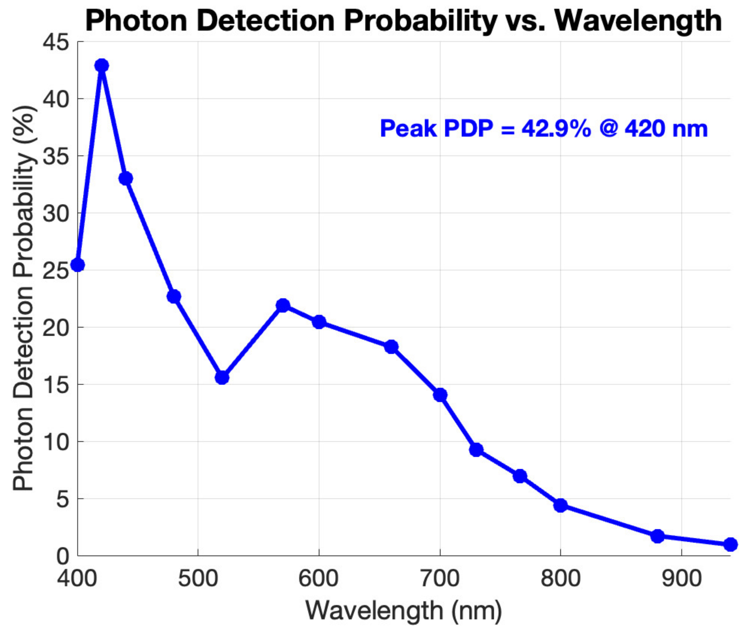
3.4. Photon Detection Probability
To measure the PDP of the SPAD with respect to wavelength, the SPAD was illuminated with continuous light from a xenon lamp that was passed through optical bandpass filters to select the wavelength and neutral density filters to adjust the optical power. An integrating sphere was used to ensure the illumination from the lamp was evenly distributed on the area of the SPAD, with controlled optical power and wavelength. As the SPAD output is a digital pulse corresponding to the detection of a single photon, it was necessary to determine the number of incident photons on the SPAD. Using a Newport 818-SL wavelength calibrated silicon photodetector (SiPD) coupled to a Newport 1830-C optical power meter, the number of incident photons on the SPAD area per unit of time was measured. Then, the DCR was subtracted from the total counts, and the ratio of SPAD pulses from photons to the total number of incident photons gives the PDP [
21]. The results of the PDP measurement for the wavelength range from 400 nm to 940 nm are shown in
Figure 12 for the median DCR pixel D1. Note that the lower range of the wavelengths that could be tested was limited by the wavelength calibrated range of our SiPD, and the upper wavelength was limited by the cut-off wavelength of silicon, as silicon becomes transparent for the photons above 1100 nm [
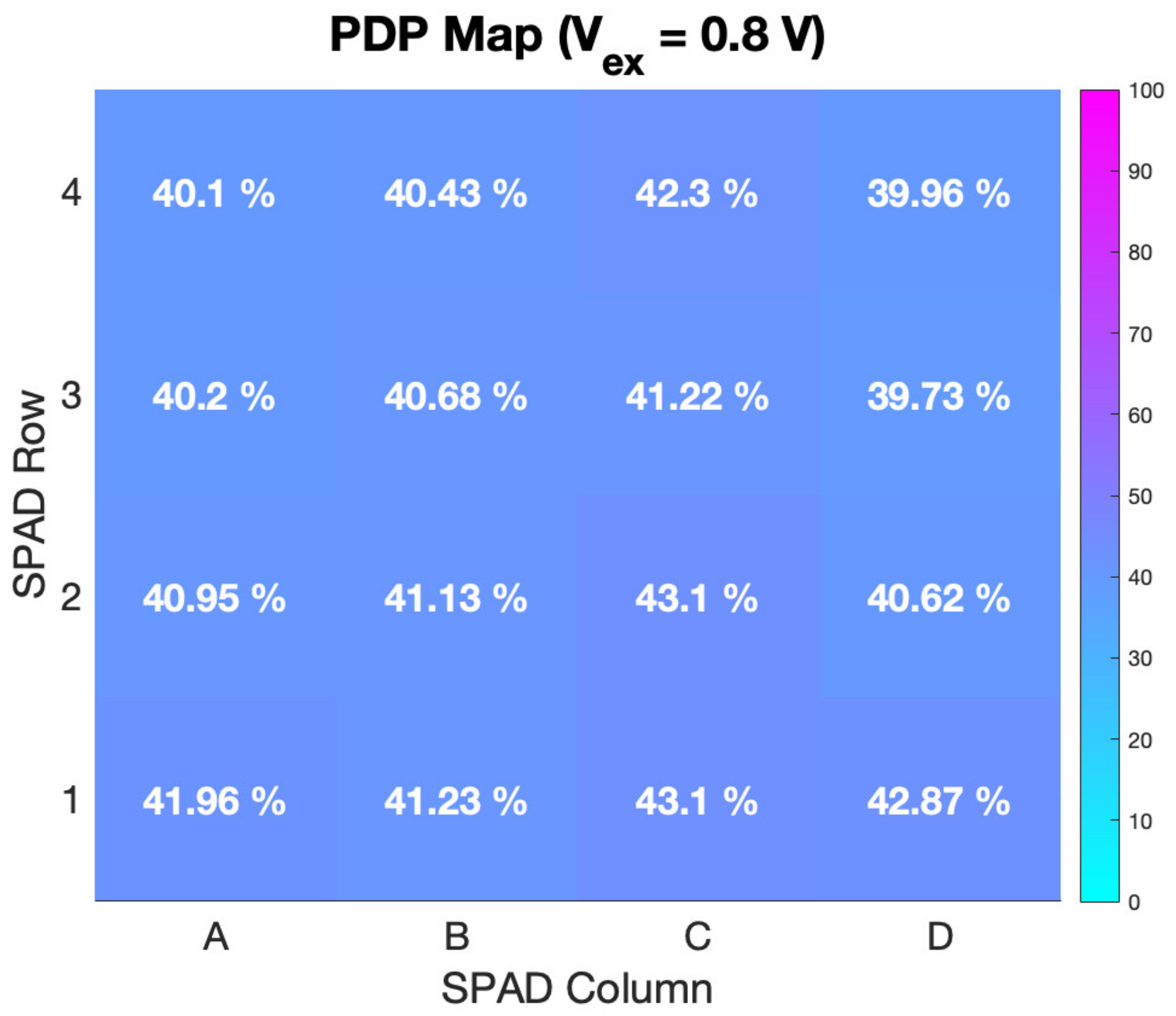
22] with negligible PDP at our maximum optical BPF wavelength of 940 nm. The peak PDP of the SPAD was determined to be 42.9% at 420 nm for the median DCR pixel with a 0.8 V excess bias. When viewing the peak PDP map in
Figure 13, it can be seen that the peak PDP is very consistent across the array, even for the noisy SPAD pixel A3. This could be an indication that the higher noise of pixel A3 is a result of an increased defect density which serves as carrier generation/recombination centers near the active area of the SPAD [
23].
The higher PDP at lower wavelengths is expected since the p+/n-well junction is close to the surface of the chip. This is also consistent with our previous n+/p-well design that exhibited a peak PDP at 440 nm [
12].
3.5. Timing Performance
To measure the timing performance of the multi-time-gated SPAD array, the same setup as for the time-gate window measurement was used. To ensure that several points could be measured for each step on the TDC quantization characteristics, 50 ps steps were used for the delay of the gate clock, and a 5% counting rate was used to reduce the influence of the SPAD’s dark noise while still avoiding pile-up distortion. For each delay setting, 500 TDC results were sampled to ensure the precision, and the statistical code density method was used to obtain the quantization characteristics [
24]. The precision is to evaluate the deviation from the mean value of a measured TDC code distribution. It should be noted that this precision includes the effect of jitter from the TDC and SPAD, as well as jitter of the measurement setup.
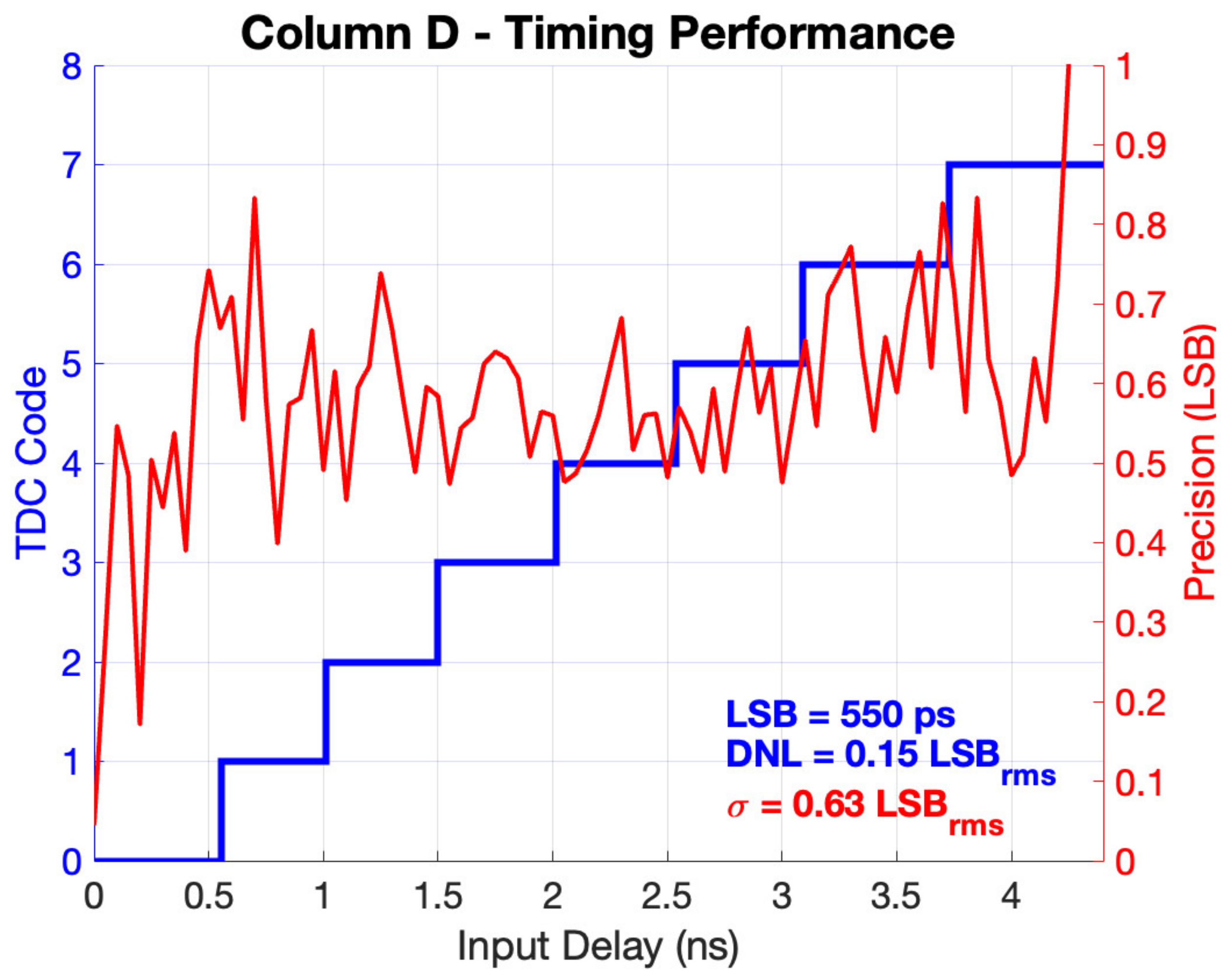
A sample of the results of TDC quantization characteristics and system timing jitter are shown in
Figure 14 for column D of the array. Due to the high consistency in the width of the gate windows, all columns of the array also showed a consistent resolution of 550 ps, with an average precision of 595 ps full-width at half-maximum (FWHM). The quantization characteristics also exhibited a mean differential nonlinearity (DNL) for the four columns of 0.24 LSB
rms. While this level of resolution is coarse, this array was designed to serve as a repeatable structure in a future large-scale array that can share a single fine-interpolating TDC. For example, a four-bit fine-interpolation TDC could then be shared by replicas of the proposed array to achieve an improved resolution of ~34 ps.
3.6. Performance Comparison
A summary of the measured results from the proposed multi-time-gated SPAD array compared to other time-gated SPAD results is presented in
Table 1.
Although the proposed array used shared circuitry to help minimize the negative impact on the array’s fill factor, the SPAD pixel was designed conservatively, resulting in a total fill factor of 9.6% for the whole 4 × 4 array. Further improvements of the array’s fill factor could be made based on an optimized SPAD design. Considering that it was designed in a fully standard CMOS process not optimized for low noise photodetection, the array achieves competitive PDP and median DCR performance of 41% at 420 nm and 37 kHz, respectively. The array also achieved a 550 ps timing resolution due to the fully integrated TDCs that are constructed from the same shared circuitry that shifts the gate windows of adjacent SPAD columns and generates the signals to trigger the time-gated front-end circuits. In future, this array can be tiled to form a larger array that shares a single four-bit fine-interpolation TDC to achieve an improved resolution of ~34 ps. Lastly, this work achieves narrow gate window widths of 4.37 ns, which can be applied at rates of up to 20 MHz. The multi-time-gated operation can allow for narrow gate widths to be used, while still covering a larger timing range, since different columns of the array cover shifted portions of the timing range.
4. Conclusions
In this work, we proposed the design of a 4 × 4 multi-time-gated SPAD array in the TSMC 65 nm standard CMOS process. While SPADs designed in custom or less advanced processes can generally achieve higher PDP and reduced noise, they generally have higher fabrication costs and less advantages to be easily integrated with the signal conditioning and processing circuits. By using time-gating techniques, the increased noise in standard CMOS SPADs can be mitigated by enabling the SPAD only during a specified time window. Time gating was also used as a means of obtaining timing information of photon events by shifting the gate window with respect to a pulsed laser. However, for a large number of timing bins, the measurement time is greatly increased. Here, we use a multi-time-gating technique to simultaneously apply shifted time gates to an array of SPADs to reduce the measurement time. As such, the gate windows can be narrowed to improve the SNR, while still covering a wide dynamic range since different SPADs cover different portions of the total range. The fabricated array achieves a median DCR of 37 kHz, 4.37 ns gate widths, 550 ps timing resolution, and a peak PDP of 41% at 420 nm, all for a 0.8 V excess bias. In future, the proposed array can be tiled to form a large-scale array that shares a single fine-interpolation TDC to achieve higher timing resolution and precision on photon events. The multi-time-gated configuration with high timing resolution and precision has a potential in the time-correlated single-photon counting applications such as diffuse optical tomography, fluorescence lifetime imaging microscopy and Raman spectroscopy.


