
A Nonisolated Transformerless High-Gain DC–DC Converter for Renewable Energy Applications
by
 , , and
Mohammad Zaid
1 ,
,
Ifham H. Malick
1,
Imtiaz Ashraf
1,
Mohd Tariq
1,*,
Basem Alamri
2 and
Eduardo M. G. Rodrigues
3,4,* 1
Department of Electrical Engineering, ZHCET, Aligarh Muslim University, Aligarh 202002, India
2
Department of Electrical Engineering, College of Engineering, Taif University, P.O. Box 11099, Taif 21944, Saudi Arabia
3
INESC-ID, Sustainable Power Systems Group, Av. Rovisco Pais 1, 1049-001 Lisboa, Portugal
4
Instituto Superior Tecnico, University of Lisbon, Av. Rovisco Pais 1, 1049-001 Lisboa, Portugal
*
Authors to whom correspondence should be addressed.
Electronics 2022, 11(13), 2014; https://doi.org/10.3390/electronics11132014
Submission received: 4 April 2022
/
Revised: 4 June 2022
/
Accepted: 6 June 2022
/
Published: 27 June 2022
(This article belongs to the Topic Power Converters)
Abstract
:Dc–dc converters with a high gain, continuous input current, and common ground are usually employed in renewable energy applications to boost the generated output voltage of renewable energy sources. In this paper, a high-gain dc–dc converter comprising a voltage multiplier cell (VMC) and a common ground with continuous input current and low-voltage stress across semiconductor devices is proposed. The converter produces a voltage gain of about ten times compared to the conventional boost converter at a duty ratio of 50% by utilizing switched capacitors and switched inductors. The simultaneous operation of both the switches with the same gate pulse offers easy and simple control of the proposed converter with a wide range of operations. The boundary operation of the converter is analyzed and presented in both modes, i.e., continuous conduction mode (CCM) and discontinuous conduction mode (DCM). Ideal and nonideal analysis of the converter is carried out by integrating real models of passive elements and semiconductor devices by using PLECS software. The simulation is also used to calculate the losses and hence the working efficiency of the converter. The performance of the converter analyzed in the steady state is compared with various similar converters based on the voltage boosting capability and switching stresses. A hardware prototype is also developed to confirm and validate the theoretical analysis and simulation of the proposed converter.
1. Introduction
High-gain boost converters have gained prominence in recent times due to their suitability in various applications such as solar PV systems [1], switch-mode power supplies (SMPS), electric vehicles, and aerospace applications. A conventional boost converter has certain shortcomings such as discontinuous input and output currents and increased losses in the system at higher duty cycle operations, which leads to its limited solar PV and fuel cell applications. The traditional quadratic boost converter (TQBC) shown in Figure 1 uses a single switch of high voltage and a current rating which results in low efficiency at higher duty ratios. In the literature, many high-gain dc–dc converters are being published [2,3] to overcome the limitations of the conventional boost and quadratic boost converter. The use of coupled inductors, Z-source converters, switched inductors, switched capacitors, and voltage multiplier cells (VMCs) are popular methods to increase the gain of high-gain dc–dc converters.
Isolated step-up quadratic boost converters are implemented in [4,5] with coupled inductors that have a high-voltage gain and low switching stress. The converter in [4] has a voltage doubler cell and produces a higher gain as compared to [5]. Soft switched dc–dc converters eliminate the switching losses [6,7] however their hardware implementation and operation are difficult. Various Z-source converters [8,9,10,11] have been proposed in the literature that contains a unique impedance network. In [10], a quasi-Z source converter is implemented using a switched capacitor and switched inductor configuration for achieving a high-voltage gain along with low-voltage stress on capacitors and a continuous input current, but the topology lacks a common ground. In [11], the hybrid quasi-Z source converter is proposed by a combination of traditional Z source converters.
A set of nonisolated switched inductors and switched capacitor converters are discussed in [12,13,14,15,16,17]. The converter proposed in [12] has a switched capacitor and quadratic gain with a common ground and low input current ripples. The converter is lightweight due to the absence of a transformer and can be utilized for solar PV applications. In [13], the authors have proposed a switched inductor boost converter that has low current stress in inductors but suffers from a low-voltage gain and high-switch stresses. In [14], the twin duty cycle and three switches configuration add to the complexity of the circuit [14,15] as compared to [16] which has two switches following the same duty cycle. A non-isolated converter is proposed in [17] and has a simple design as compared to [15,16] along with a high gain and reduced voltage stresses on switches, diodes, and capacitors. It has a symmetrical structure that helps to ease the choice of the components and its design. In [18], a single switch nonisolated topology is implemented with low switch stress. In [19], the transformerless converter shown in Figure 2 is proposed. It consists of a VMC, with a gain of six times that of a conventional boost converter with a single switch and two inductors. The converter shown in Figure 2 has a single switch but the converter lacks a common ground. Moreover, the input current pulsates. The converter proposed in this paper has a common ground and continuous input current.
In [20], a modified ćuk converter is proposed with switched capacitors. The authors have proposed a buck-boost converter in [21] for renewable energy applications with continuous input. The converter exhibits high efficiency above 95% around the 56.5% duty cycle; however, the switching stress also increases drastically. In [22], an extendable boost converter employing active-passive inductor cells (APIC) is proposed. The efficiency and voltage gain at a lower duty ratio decrease drastically as the number of APICs is increased. The authors in [23] have introduced an extended boost converter by implanting a cell consisting of switched capacitors and inductors between a conventional boost converter. The converter has the same voltage gain for the complementary duty ratio, which is nearly constant, while the duty ratio is varied from 30% to 70%. A quadratic boost converter is proposed in [24]. The gain of the converter is lower as compared to similar topologies. A variety of quadratic boost converters are introduced in [25,26,27,28,29,30], each with its set of advantages and disadvantages. The authors in [25] have proposed a simple quadratic boost converter, but it lacks a common ground, whereas a modified quadratic boost converter in [26] is implemented, resulting in twice the gain as compared to the quadratic boost converter. The converter proposed in [27] has a common ground but a lower gain as compared to the topology proposed in [28], which lacks a common ground. The quadratic converter proposed by the authors in [29] has more components as compared to [30] but has a higher gain at the cost of a decreased efficiency due to increased heat losses.
In this paper, a new transformerless high-gain dc–dc converter is implemented that employs a VMC to boost the voltage. The attractive features of the proposed topology are
- The converter achieves a high gain of 10 times the conventional boost and 5 times that of the quadratic boost converter at a 50% duty ratio.
- The converter has low voltage stress of 5% of the output voltage across switch S1.
- The converter uses the same gate signal for both switches, which leads to its easy operation.
- The topology has a continuous input current and a common ground, making it feasible for PV applications.
The paper discusses the structure of the proposed topology and its detailed ideal analysis in Section 2 followed by the nonideal analysis in Section 3. The comparison of the proposed topology with various similar converters is carried out in Section 4. The simulation and the experimental results are presented in Section 5 along with the efficiency of the proposed converter at different input voltages and power.
2. Structure of Proposed High-Gain DC–DC Converter Topology
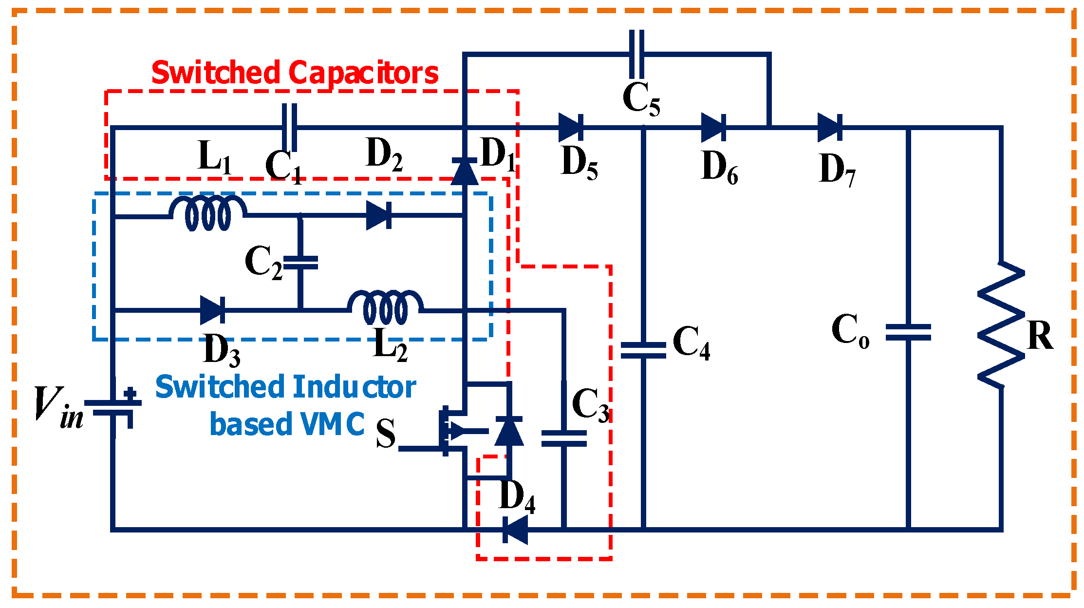
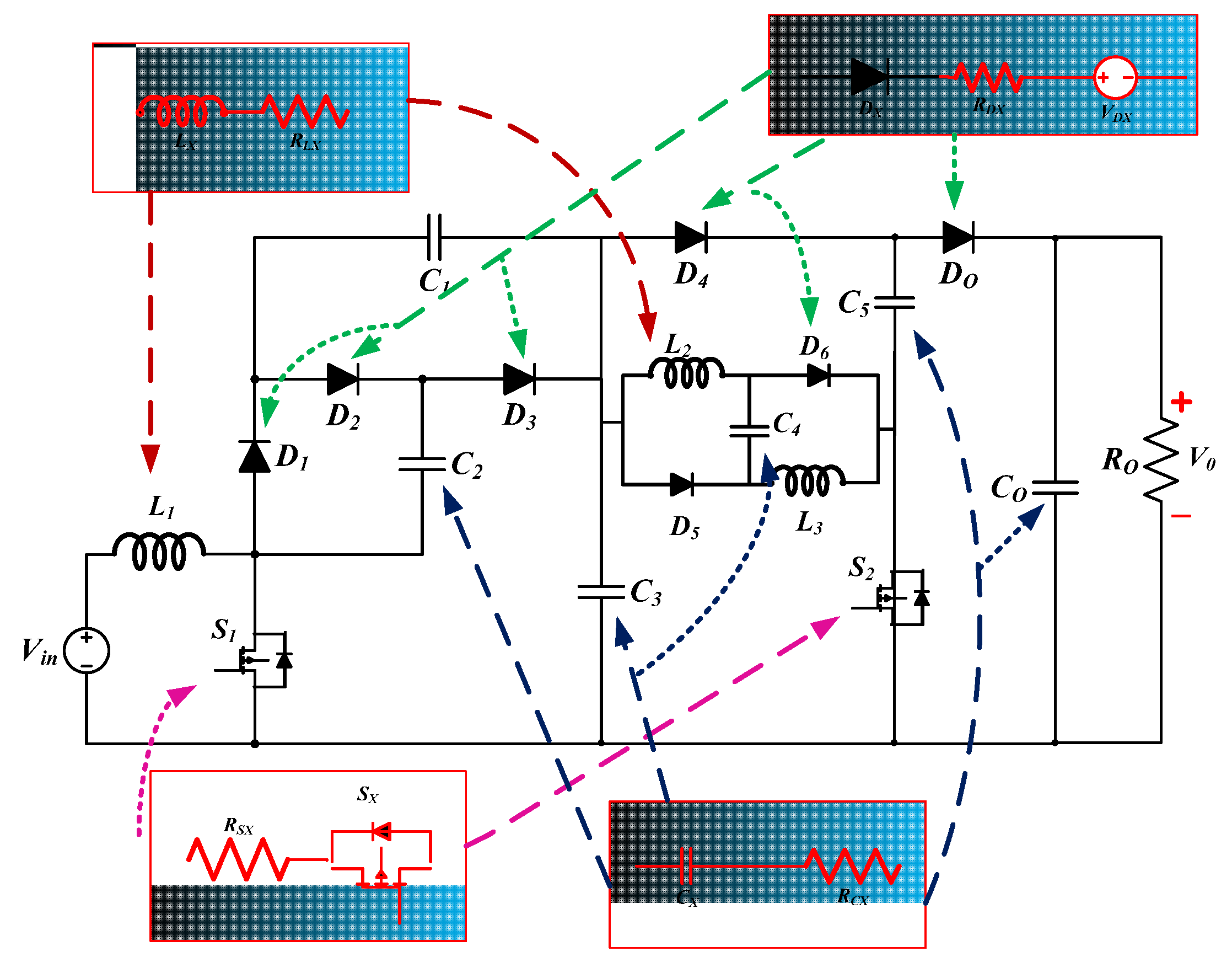
The components of the proposed nonisolated dc–dc converter topology depicted in Figure 3 consist of a fixed DC input voltage source Vin; two switches (MOSFETs) and ; three inductors , , and ; seven diodes , , , , , , and ; five capacitors , , , , and ; and a resistive load with an output voltage of VO. The circuit also consists of a VMC with elements , , , , and . The nonisolated converter does not include a high-frequency transformer and hence contributes to its low bulkiness, size, and cost reduction. This further aids in easier control of the topology as compared to isolated converters.
2.1. Operation of the Converter in Continuous Conduction Mode (CCM)
The proposed converter operates in two modes in each cycle while working in the CCM state. Each mode is discussed in detail by providing the voltage and current equations of each component in both modes.
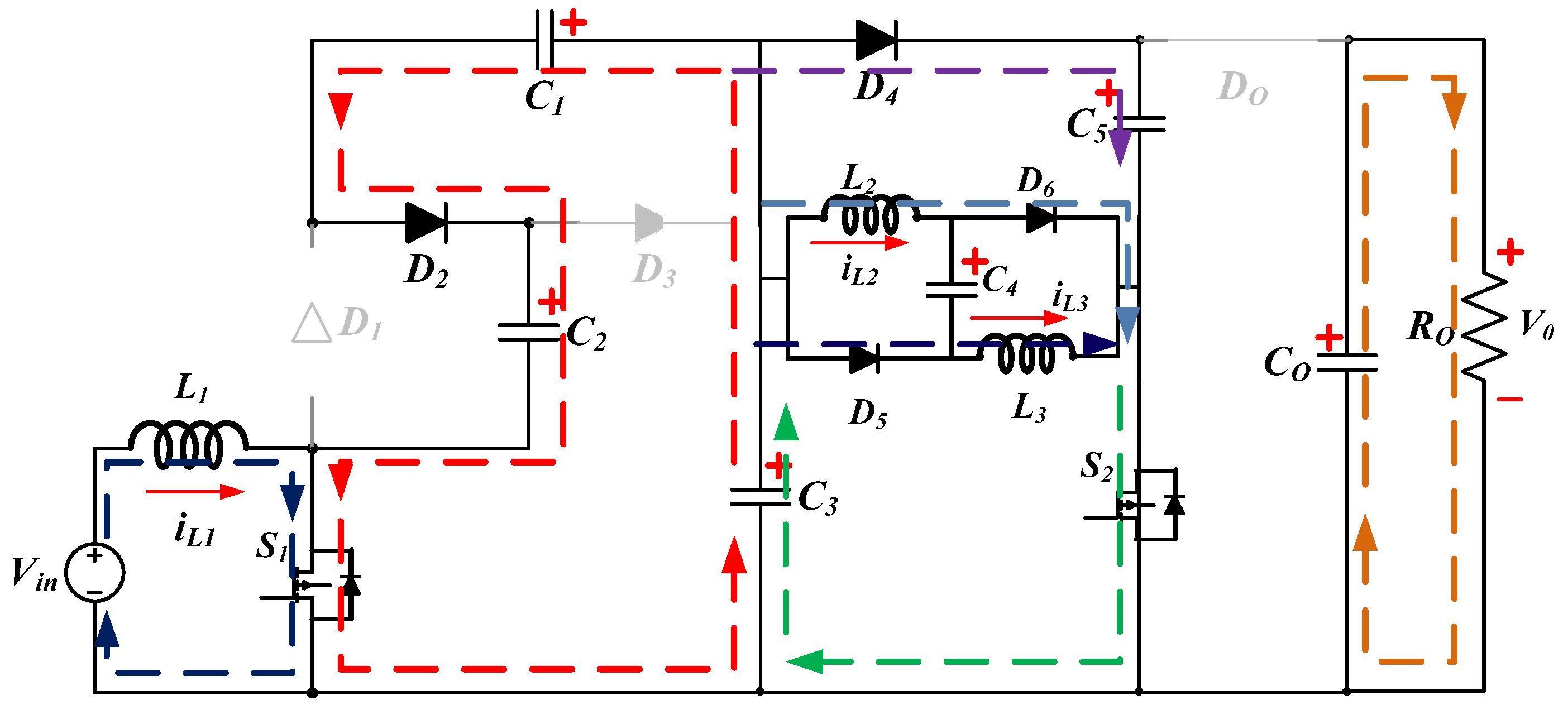
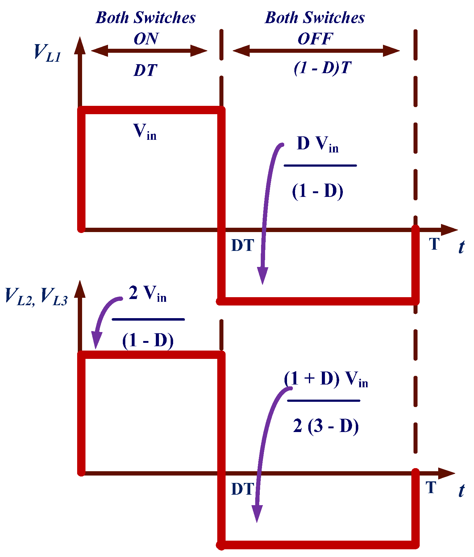
Mode 1 (): In mode 1, both switches and are turned ON simultaneously, as shown in Figure 4, by applying the appropriate gate pulse. In this mode, diodes , , , and are forward-biased, whereas the other diodes , , and are reverse-biased. The inductor is charged through the input voltage source and the inductors and are charged through the capacitor . The capacitor is discharged, while the capacitor is charged in this mode. The output capacitor discharges and feeds the load to maintain a constant voltage across the output load resistor.
The voltage and current equations across the inductors and capacitors during mode 1 when both switches are ON can be expressed as (1) and (2), respectively.
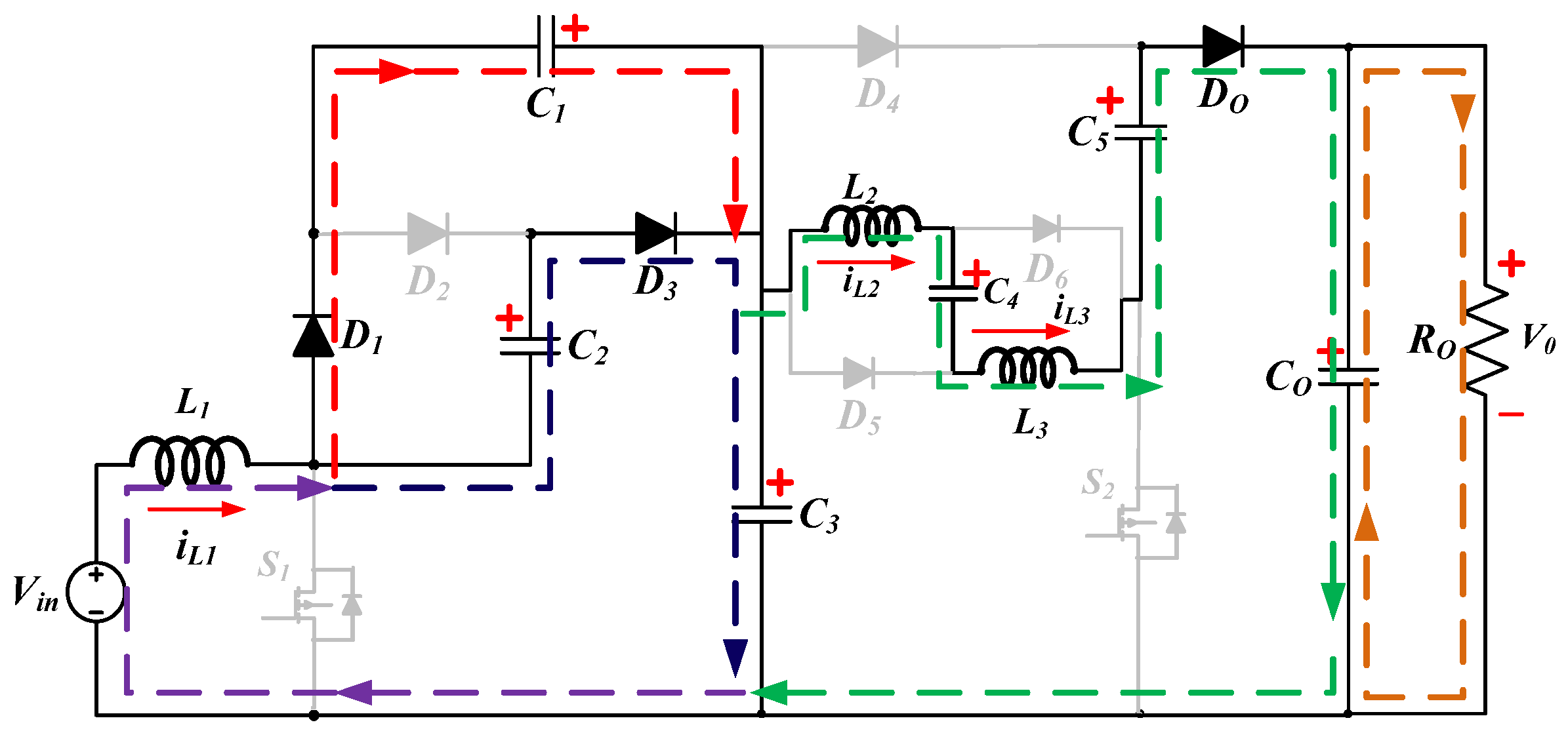
Mode 2 (): In mode 2, both switches and are turned OFF simultaneously. In Figure 5, it can be seen that diodes , D3 and DO are forward-biased, whereas the remainder of diodes D2, D4, D5 and D6 are reverse-biased. In this mode capacitor, is charged through capacitors and . Inductors and along with capacitor transfer power to load and charge, and capacitor maintains a constant voltage about the load. The voltage and current equations across the inductors and capacitors during Mode 2 when both switches are OFF can be expressed as (3) and (4), respectively.
The ideal voltage gain (M) can be calculated by using the volt-sec balance principle in an inductor in CCM operation as per the following relation given in (5),
Applying the volt-sec principle in the inductor
Applying the volt-sec balance principle to
Equating Equations (6) and (7)
where ‘D’ denotes the duty cycle for switches and .
The voltages across the capacitors and inductors (shown in Figure 6) are represented in (9) and can be easily evaluated by applying KVL in respective loops as,
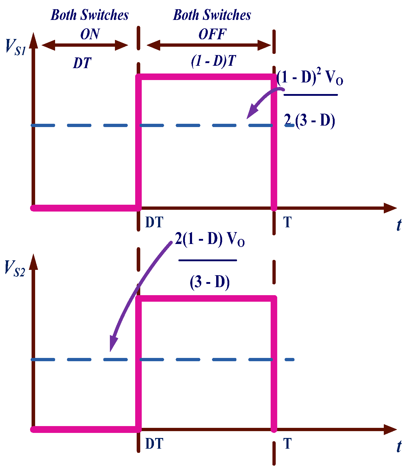
2.1.1. Calculation of Voltage Stress
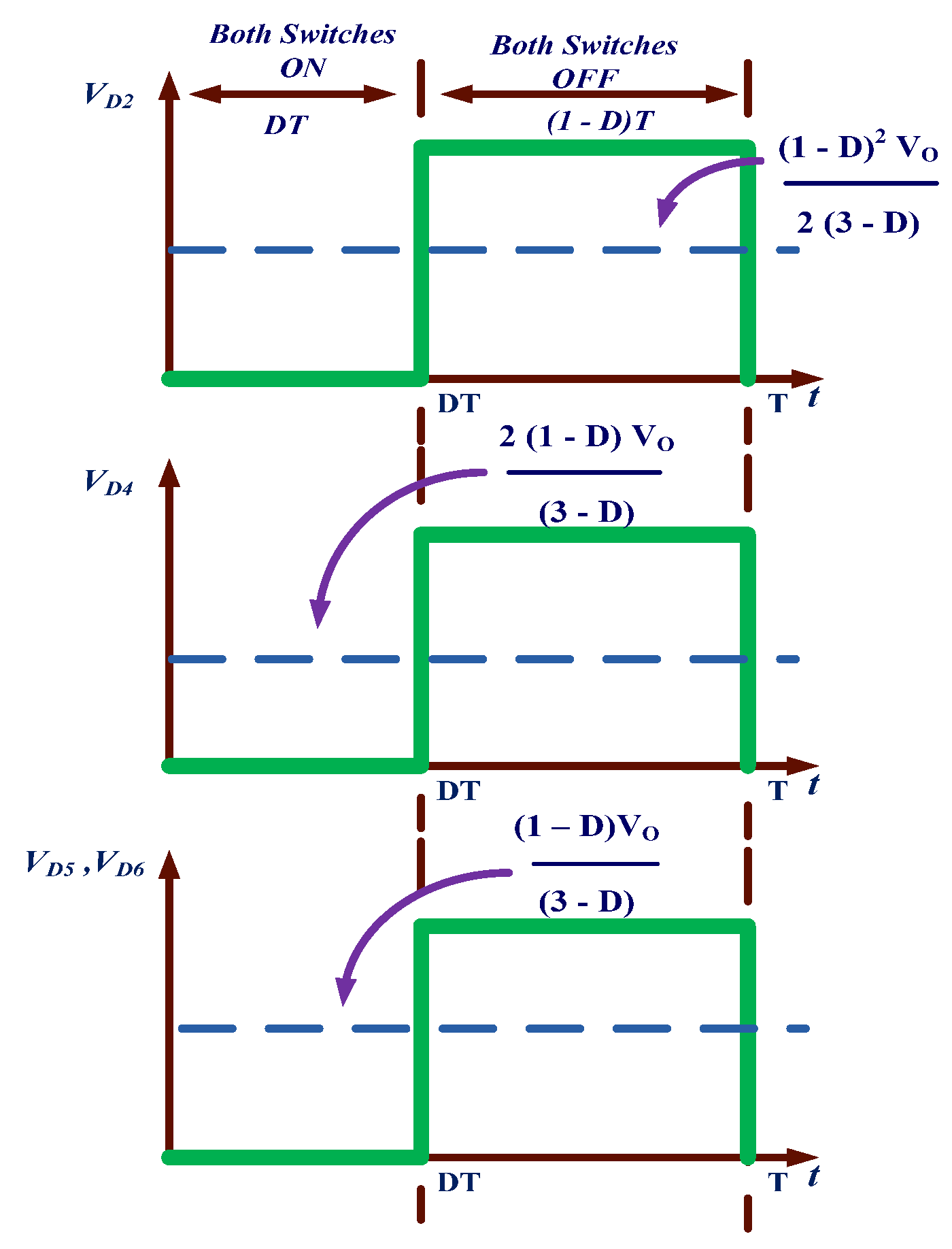
The voltage stress across the switches as shown in Figure 7 and the diodes shown in Figure 8 and Figure 9 are evaluated at the instance when the switches are not conducting and are in the OFF state. The voltage stress particularly refers to the peak inverse voltage across the switch.
The voltage stresses across the switches in the OFF state are given as,
The voltage stress across different diodes when they are not conducting can be expressed as in (11):
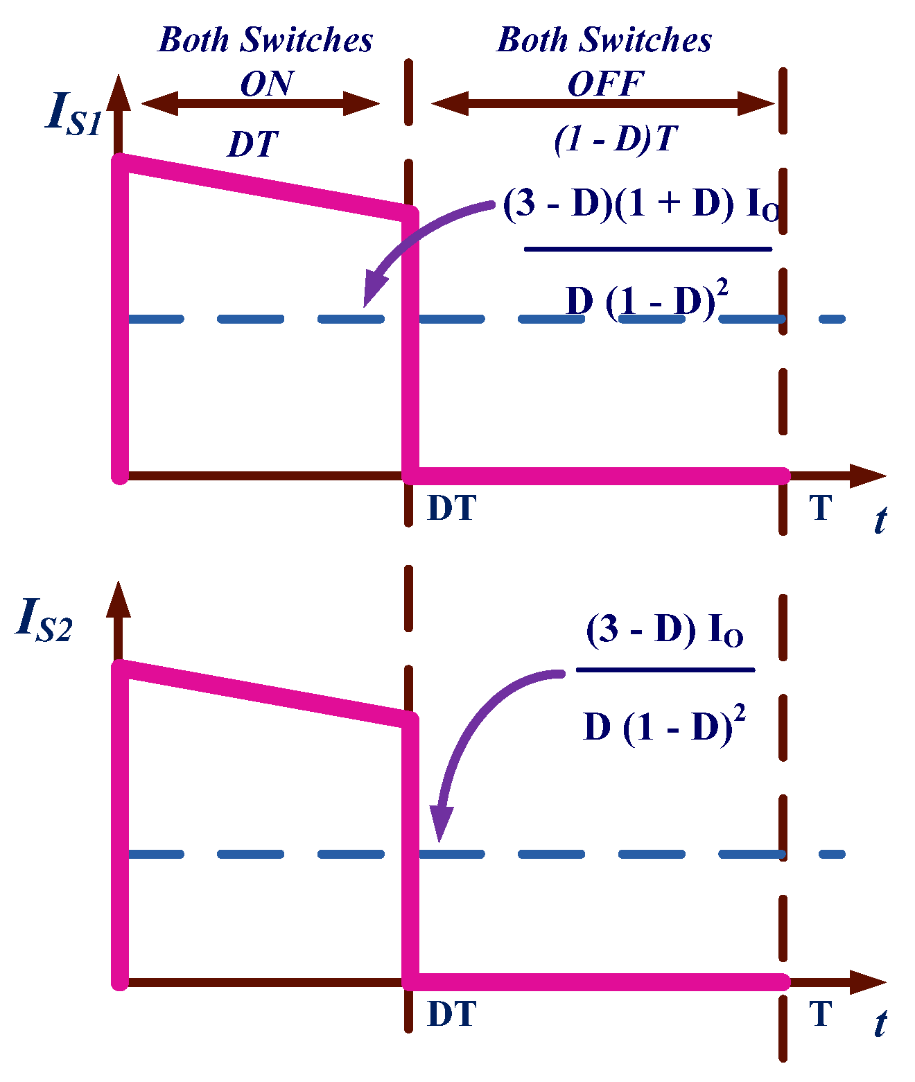
2.1.2. Calculation of Average and RMS Currents
The average currents through the capacitors and switches can be easily determined by applying the current-sec balance principle in capacitors.
The average switch currents (in Figure 10) are given as,
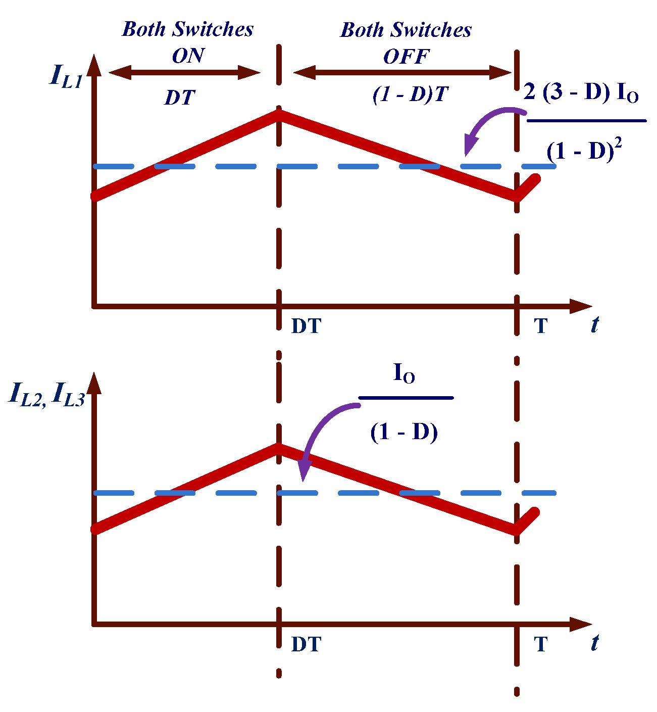
The average inductor currents (in Figure 11) are given as,
The RMS values of the switch currents are given as,
The RMS values of the various currents through the components are given as,
2.1.3. Design of Inductors and Capacitors
The ripple current in the inductor can be found as in (17) and rearranged to obtain the critical value of the inductor for CCM operation.
The ripple current and the critical value of the inductors and can be found as
The peak-to-peak ripple voltages across the capacitors can be given as
2.2. Operation of Converter in Discontinuous Conduction Mode (DCM)
The proposed converter can also operate in DCM. This mode consists of three different sub-modes of operation, as depicted in Figure 12.
- (i)
- Mode 1: In this mode, both switches are turned ON for duty cycle D as in the case of CCM.
- (ii)
- Mode 2: In this mode, both switches are turned OFF and the inductors start discharging. The inductors discharge through diodes , , and for a duty cycle D’ and the mode ends at D + D’.
- (iii)
- Mode 3: In this mode, none of the switches or diodes conduct, and the load is fed entirely through the output capacitor . The mode is operated for a duration of 1 − D − D’.
The inductors are charged in Mode 1 (from t = 0 to t = DT) and are discharged in Mode 2 (from t = DT to t = D’T). Hence, by applying volt-sec balance across the inductors, we obtain the voltage gain in DCM.
Applying volt-sec balance in inductor L1, we obtain,
Applying volt-sec in L2, we obtain,
From Equating (20) and (21), we obtain,
Rearranging Equation (22), we obtain,
Under DCM analysis for inductor , we have,
For DCM operation,
From (24) and (25) we obtain,
where is the time constant represented as and is the switching frequency of the switches.
Equating (25) and (26), we obtain,
Let ; then,
2.3. Converter Operation at Boundary Conditions
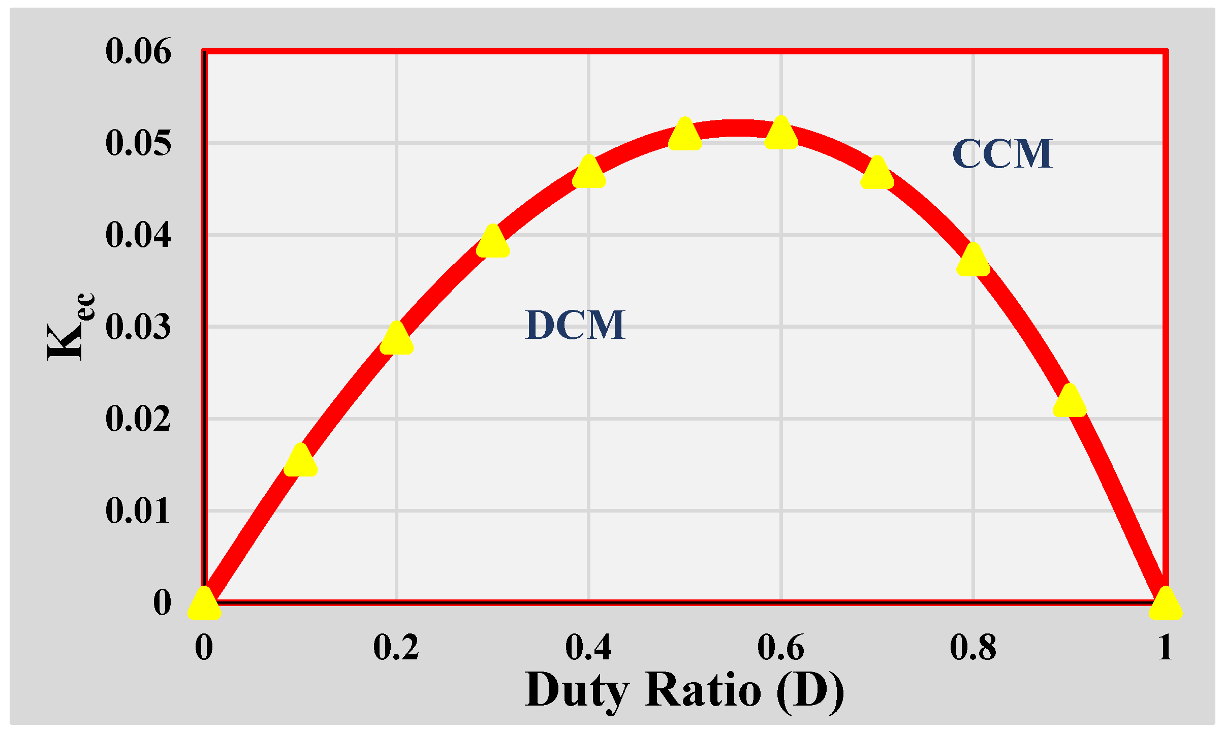
The boundary condition represents the critical conduction state of the converter on the boundary of DCM and CCM. The relation for the boundary condition can be easily formulated by equating the voltage gains in the CCM and DCM operations, respectively. The boundary condition is determined by the boundary-normalized time constant of the inductor , is as shown in Figure 13. The variation in the time constant of the inductor as a function of the duty cycle is represented as
The maximum value of is 0.00516 obtained at D = 0.55. The converter operates in DCM mode for a time constant less than and in CCM mode for a time constant more than .
3. Nonideal Analysis
The nonideal analysis of the converter accounts for the power loss analysis of the circuit. Thus far, only the ideal lossless analysis of the converter is being considered in the paper, ignoring the parasitic series resistances of the inductors, equivalent series resistance (ESR) of the capacitors, barrier potential voltage and leakage resistances of the diode, and the ON-state resistance of the switches (MOSFET), as shown in Figure 14. The loss analysis is proceeded by the inclusion of the above-mentioned parameters in the ideal circuit of the proposed topology. The nonidealities of the elements tend to decrease the voltage gain of the converter and also result in an increase in power losses. The total power loss across all the elements is given as,
3.1. Calculation of Losses across Switches
The losses across switches can be either conduction losses that are encountered when the switch is ON and current flows through it, or they may be switching losses that are encountered when the switch is in the transition from the ON state to OFF state or vice-versa.
For the conduction loss calculations, the resistance of both switches is assumed to be the same, i.e.,.
For the calculation of switching losses for a switch operating at a switching frequency of , the rise time () and fall time () of the gate pulses are considered. Then, the switching losses can be given as,
3.2. Calculation of Losses across Diodes
For the calculation purpose, the cut-in voltage and resistance of all diodes are assumed to be the same, i.e., and = = = = = = = . The losses across different diodes are given as:
3.3. Calculation of Losses across Capacitors
For the calculation of conduction loss in capacitors, the parasitic resistances of the capacitors are assumed to be equal, while the resistance of the capacitor CO is assumed to be rCO
3.4. Calculation of Losses across Inductors
The loss calculations for inductors are carried out by ignoring the ripple in the inductor current through the leakage resistances Inductors and have the same design values; hence, their parasitic resistances are assumed to be equal.
3.5. Calculation of Efficiency of the Converter in Nonideal Mode
The efficiency of the converter is given as the ratio of the output power transferred to the total input power fed to the circuit, which can be represented as the sum of the output power and the total losses in the converter. The efficiency () is given as
where K is a constant given simplified as,
After substituting the value of K obtained in (45) in (44), we obtain,
where,
3.6. Calculation of Nonideal Voltage Gain
For the derivation of nonideal voltage gain, all the lossy components of the elements such as the ON-state resistance of diodes and switches, ESRs of the inductor, and capacitor are considered for the analysis. Thus far, the input and output powers are equal due to lossless analysis, whereas, considering the above assumptions, the modified relation between the input and output power can be expressed as:
Input Power = Output Power + Losses across elements
3.7. Variation in Nonideal Voltage Gain
The nonideal gain of the proposed converter is derived as,
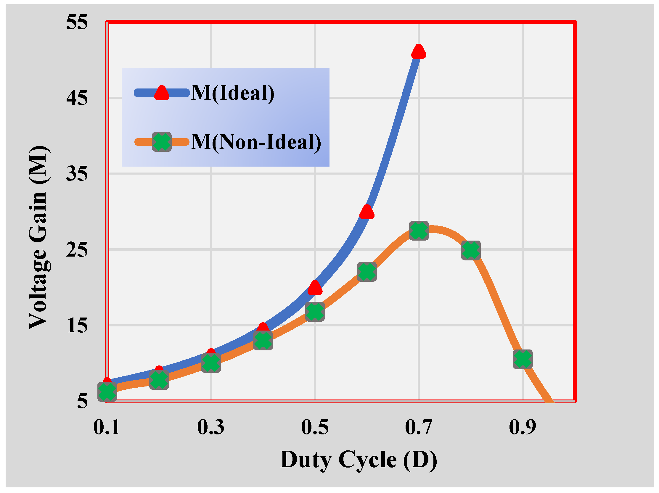
From the voltage gain comparison of ideal and nonideal voltage gains of the proposed topology in Figure 15, it is observed that both gains have similar values up to the duty ratio of 0.4, and then the nonideal gain increases until D = 0.7 but deviate from the ideal characteristics. Thereafter, it gradually decreases to zero at the unity duty ratio.
The voltage gain of the converter can be affected by the parasitic resistances of different elements of the converter such as the parasitic resistance of inductors, capacitors, and switches. As the parasitic resistances of different elements increase, the voltage gain of the converter decreases gradually.
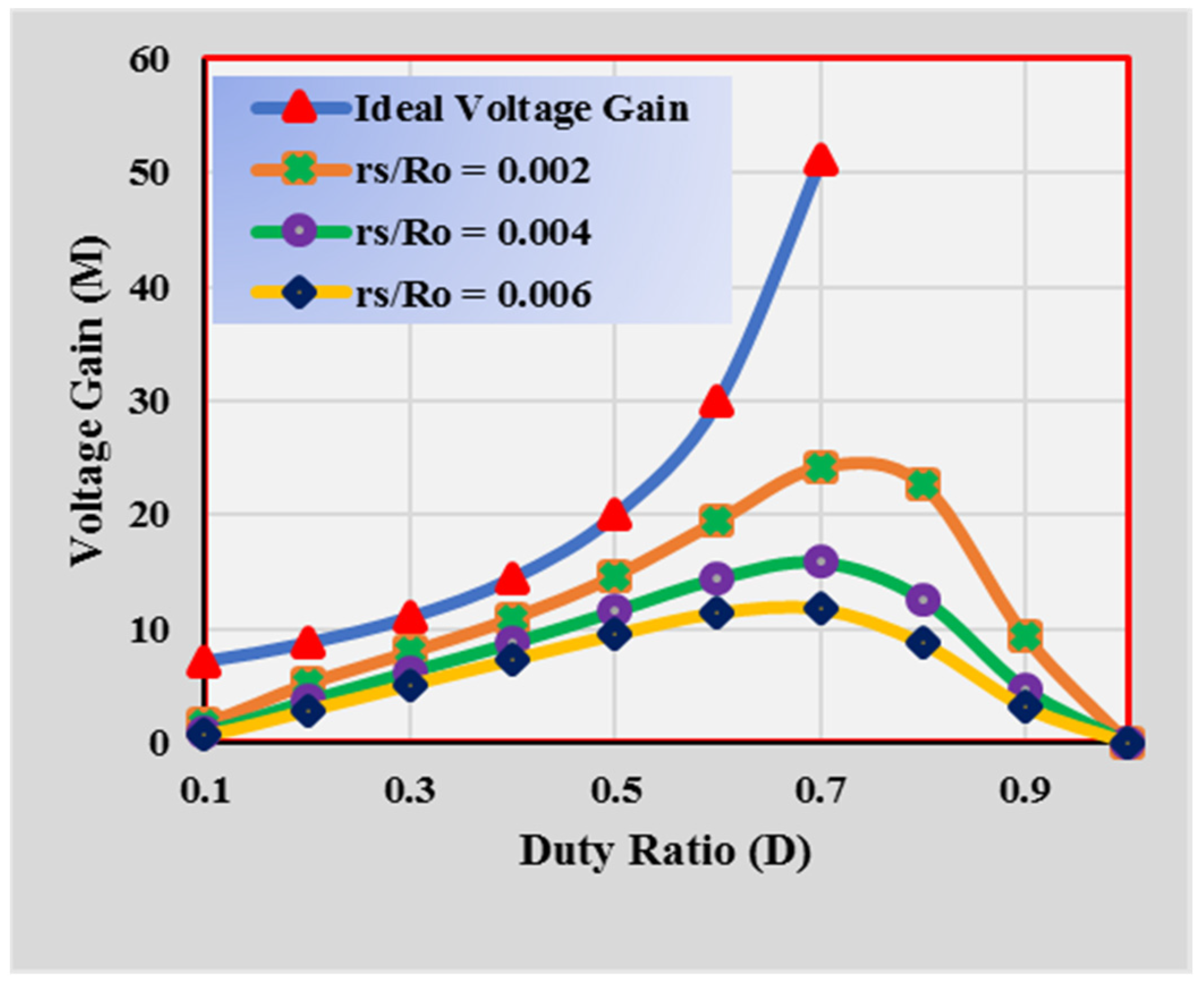
From Figure 16, it can be observed that, when the parasitic resistance of the switch is increased while other elements are kept ideal, the voltage gain of the converter decreases. For the parasitic resistance of 0.2% of the load resistance, the maximum gain is at the duty ratio of 0.7 with a gain of 24.18, while it decreases to 15.84 and 11.77 for 4% and 6% of the parasitic resistance, respectively, at D = 0.7.
From Figure 17, it can be observed that, when the parasitic resistance of the inductor is increased while other elements are kept ideal, the voltage gain of the converter decreases. For a parasitic resistance of 0.2% of the load resistance, the maximum gain is at the duty ratio of 0.75 with a gain close to 34, while it decreases to 24.88 and 19.80 for 4% and 6% of the parasitic resistance, respectively, at D = 0.7.
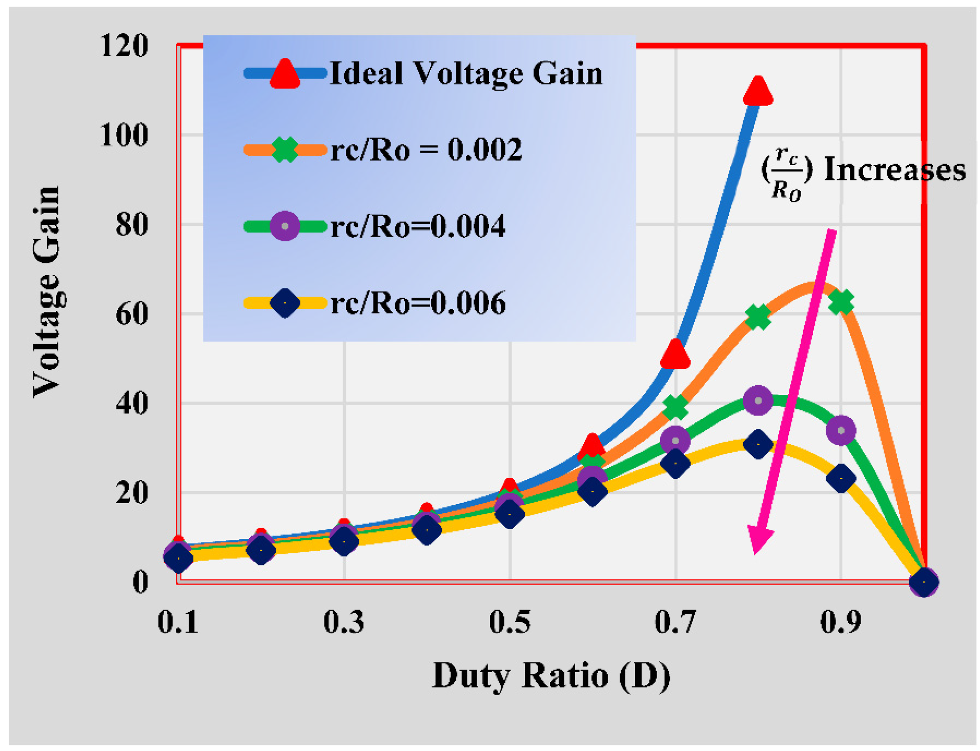
From Figure 18, it can be observed that, when the parasitic resistance of the capacitor is increased while other elements are kept ideal, the voltage gain of the converter decreases. For the parasitic resistance of 0.2% of the load resistance, the maximum gain is at the duty ratio of 0.8 with a gain of 63, while it decreases to around 41 and 21 for 4% and 6% of the parasitic resistance, respectively, at a near-duty ratio of 0.8.
4. Comparison of the Proposed Topology
In this section, a comparison between the proposed topology with two traditional topologies and recent topologies is discussed. The topologies are compared based on their voltage gain (MCCM), number of inductors (NL), number of capacitors (NC) and number of diodes (ND) in the converter. The voltage stress appearing across the switches (Vsi/Vin) is also compared along with the availability of common ground.
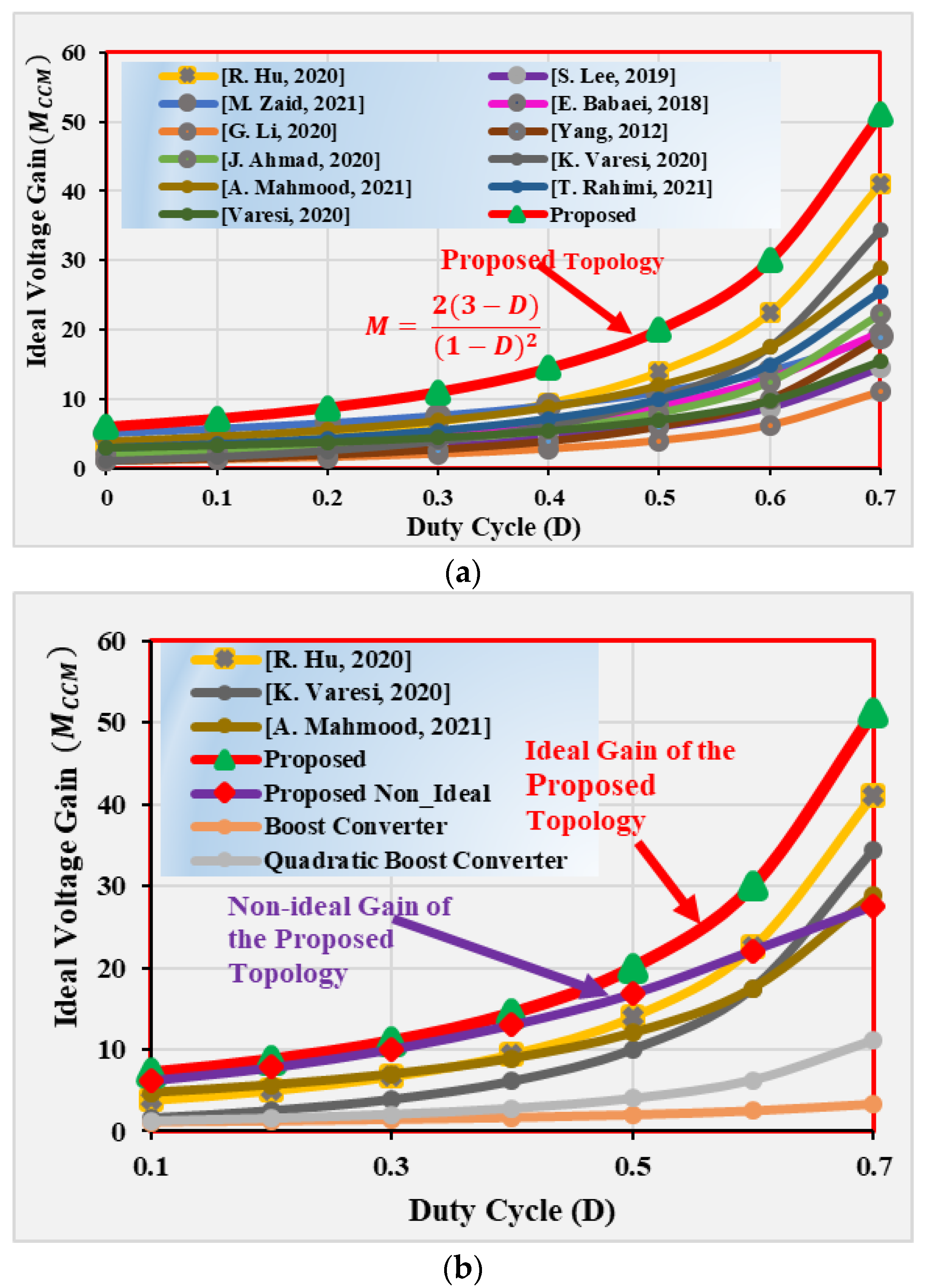
For the comparison of the topologies, the graph between the ideal voltage gain and the duty cycle is plotted in Figure 19a. Figure 19b depicts the comparison of the nonideal gain of the converter with the ideal gain of some selected topologies whose gain intersects the nonideal gain plot of the proposed topology. The voltage stress across the switches in the compared converters is shown in Figure 20.
It can be observed from Figure 19a that the proposed topology has the highest ideal gain among all the high-gain boost converters compared to all converters. An ideal voltage gain of above 14 is achieved by the proposed topology at a duty ratio of 40% and a gain of 20 is achieved at a duty ratio of 50%. The proposed converter also has a higher nonideal gain, as shown in Figure 19b, as compared to the ideal gain of the similar topologies, as presented in Table 1, until the duty ratio of 60%. The switching stress of the converter is very low as compared to the traditional topologies. In converters [4,5], even with the presence of an isolation transformer/coupled inductor operating at a transformation ratio of one, a lower gain than the proposed topology is produced, which works without a transformer or coupled inductor, hence reducing the overall cost of the topology.
For n = 1, the ideal gain of the converter in [4] when compared with the gain of the proposed converter is found to be half. Moreover, the voltage stress across the switch S1 in [4] increases significantly as shown in Figure 20.
The topology proposed in [16] also has a VMC and two switches and produces a high gain at lower duty ratios with a lower number of components as compared with the proposed topology, but it decreases as the duty ratio is increased above 40%. The proposed converter despite having fewer inductors, switches and diodes than the converter [22] is capable of producing a much higher voltage gain. Although the switch stress across the converter [22] is very low as compared to the proposed one, the converter lacks a common ground that is available in the proposed topology. The converters in [24,25], despite having 2 and 3 inductors respectively and 2 switches which is the same as used in the proposed topology, produce a lower gain than the proposed topology and, concurrently, the voltage stress across the switch.
In the case of the topology shown in [25], the switch stress increases after a conversion gain ratio of 14. The converters in [26,27] also have three inductors but suffer from a low-voltage gain. The switch S1 of [27] has high-voltage stress after a voltage gain of 8. The quadratic boost converter in [29] has the same inductors as the proposed converter, but the voltage gain is half as compared to the proposed converter, and it has a single switch only. The topology in [29] exhibits high-voltage stress across switch S2 amongst all the compared topologies. The topology in [30] has the least voltage stress across its switches but suffers from a low ideal voltage gain, which is much lower than the nonideal voltage gain produced by the proposed converter.
From the comparison, it can be inferred that the topology has the highest voltage gain and the switch voltage gain across is very low. The switch voltage gain across the switch is found to be high for low-voltage gains, but it does not increase further as the voltage gain increases beyond 15. Hence, the proposed topology can be used at a voltage gain higher than 14, which is easily achieved at any duty ratio beyond 40%. Moreover, continuous input current and common ground are other advantages of the proposed converter.
5. Results
In this section, we discuss the simulation results performed on the Piecewise Linear Electrical Circuit Simulation (PLECS) and the experimental results obtained on hardware set-upfor the proposed topology.
5.1. Simulation Results
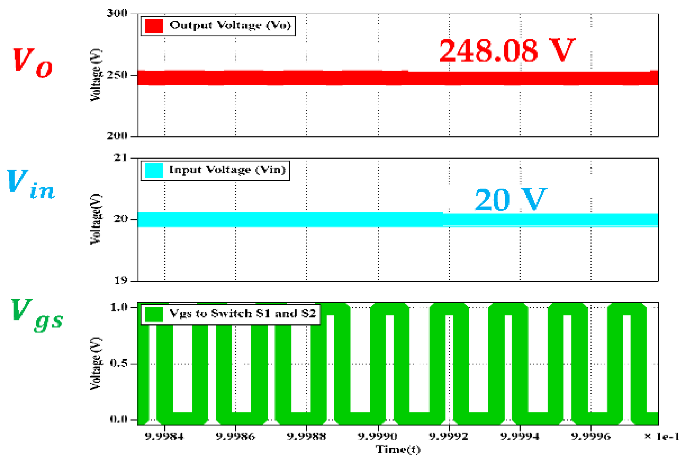
In this section, the simulation results of the proposed converter are presented. The simulation was carried out in PLECS software at an input voltage of 20 V and switching frequency of 50 kHz. The duty ratio was maintained at 0.4. The value of the inductor was 330 μΩ and its parasitic resistance was maintained at 0.12 Ω, while the value of capacitors was 47 μΩ and its parasitic resistance was kept at 0.1 Ω. The ON-state resistance of the switches was found to be 70 mΩ. With the above parameters, the simulation was performed and the output voltage was found to be at a 40% duty ratio with , which can be seen in Figure 21.
In Figure 22, the inductor current through inductor L1 was found to be and for inductor L2. The ripple in the current through the inductor was lower and, hence, the average and RMS values were found to be the same.
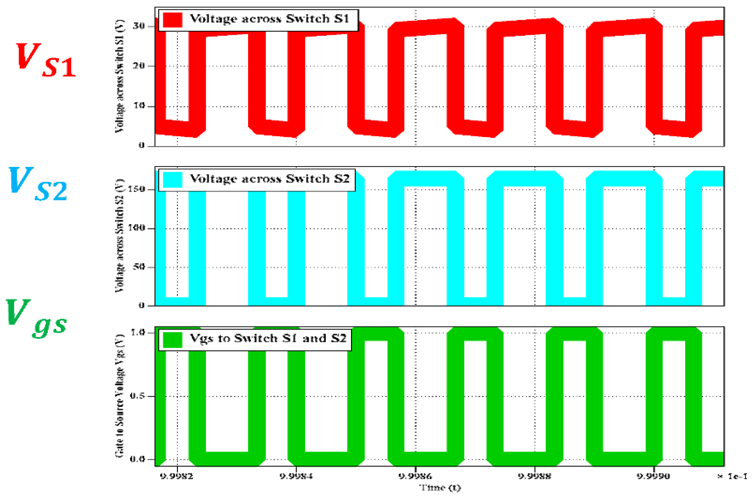
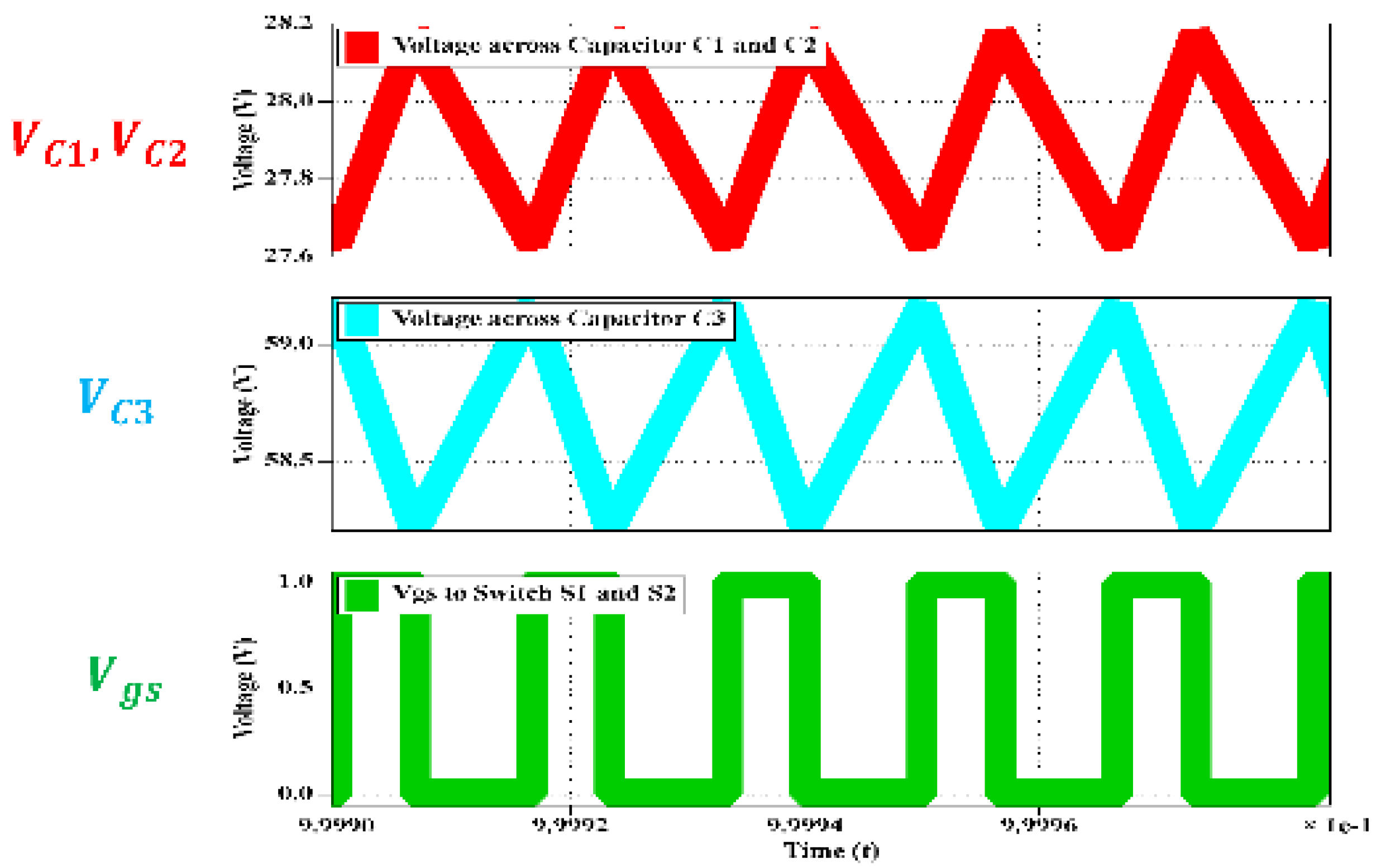
From Figure 23, the peak voltage across switches S1 and S2 was found to be and , respectively, while the RMS voltage was . and , respectively. From Figure 24, the average capacitor voltages in the simulation were found to be and , while from Figure 25, the capacitor voltages were , , and . The ripple in capacitor voltages was negligible and, hence, the RMS and average voltages were found to be the same.
5.2. Experimental Results
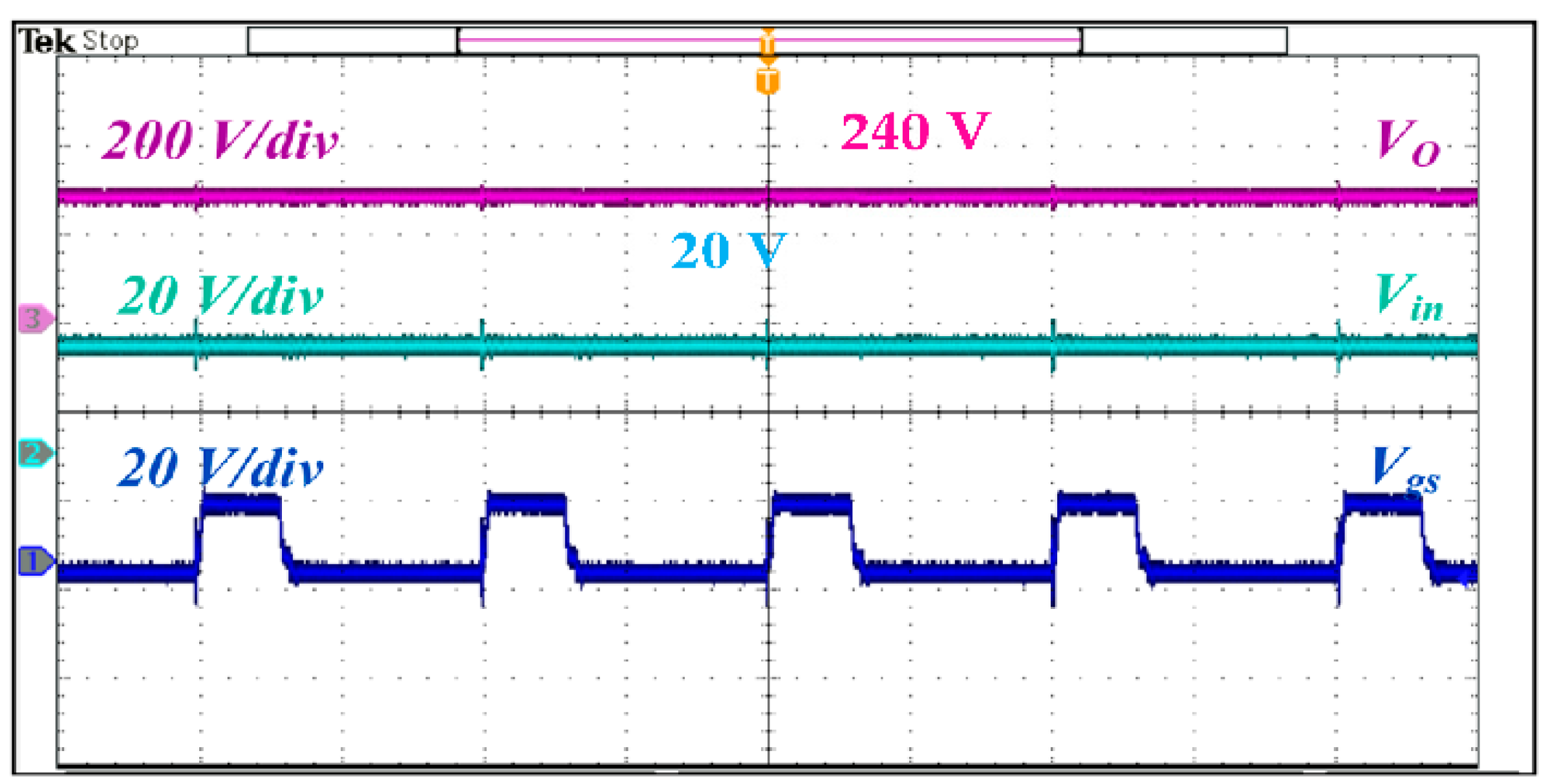
The experimental analysis of the proposed converter was carried out on the same parameters as the simulation procedure. To verify the overall voltage boosting, continuous current, and capacitor voltage handling capability of the proposed converter, a hardware prototype of the proposed converter was tested under standard laboratory conditions with the parameters mentioned in Table 2. To demonstrate the working of the topology, a converter with an output power of 200 W at a duty ratio of 40% was implemented with a load resistance of 300 Ω. For switches and , Power MOSFET with part number SPW52N50C3 provided with a duty cycle (D) of 0.4 operating at a switching frequency (fs) of 50 kHz was used, whereas diodes () with part number HER806 were used. From Figure 26, a 20 V DC supply was used at the input side and an output of 240 V was obtained for the same with as the gate drive signal.
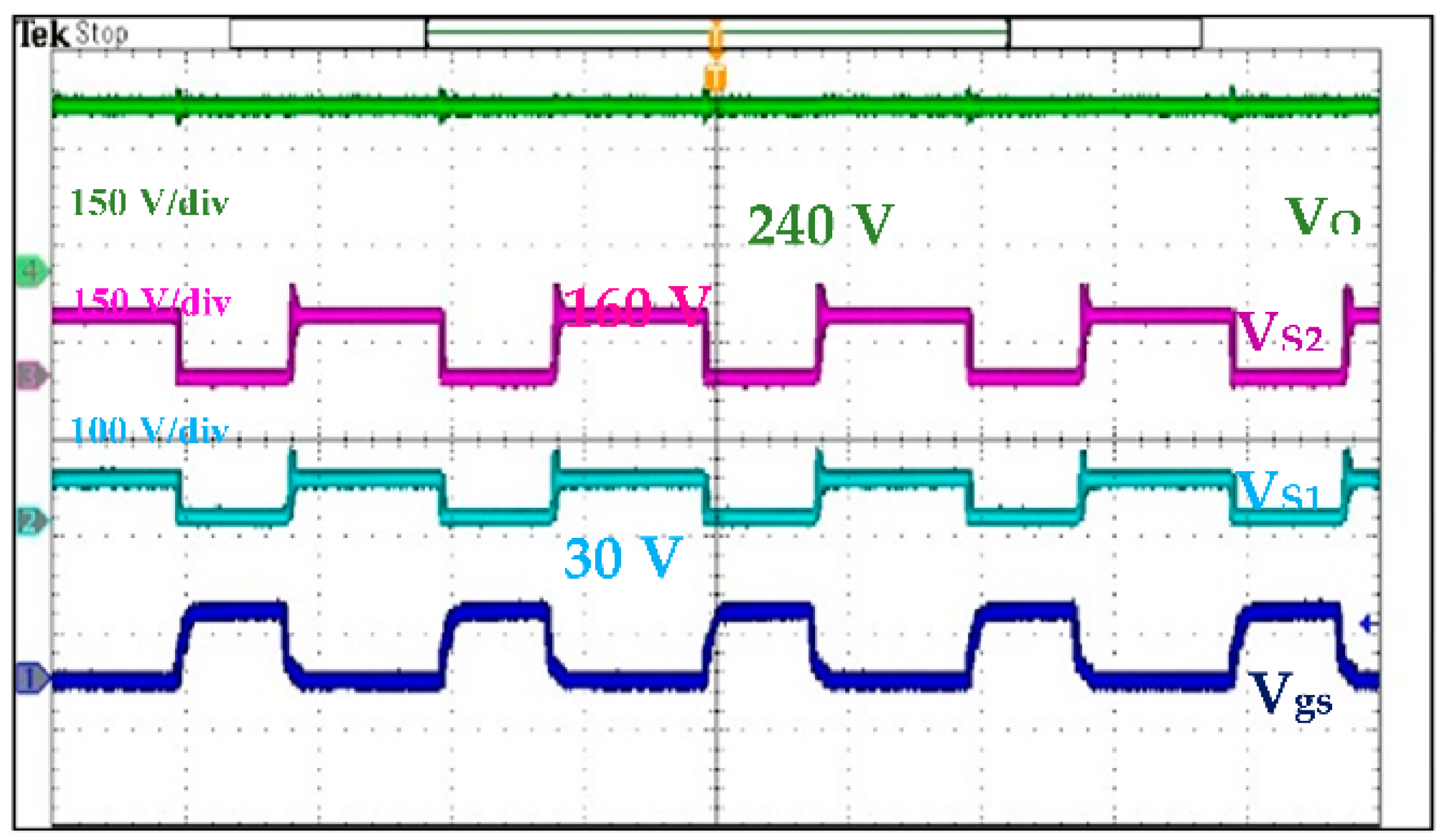
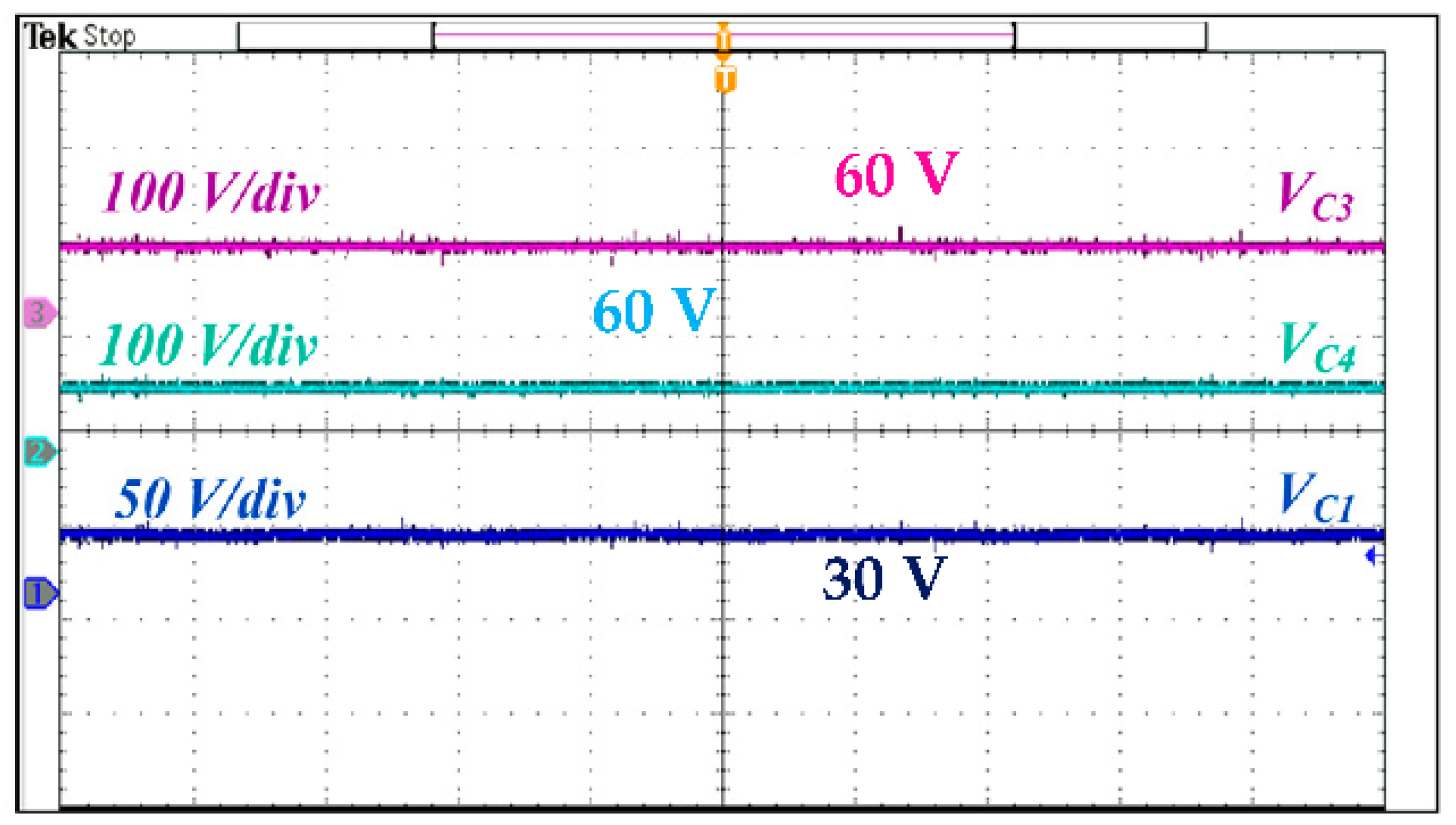
From Figure 27, when the switches are ON, the inductors become charged and the current through them increases. For inductor , it increases from an initial value of 4.8 A to a peak value of 5.2 A and it increases from an initial value of 0.7 A to a peak value of 1.0 A for inductors L2 and L3. When the switches are OFF, the inductors release their stored energy, and the currents through them decrease back to their initial values. During the OFF state, the switches are reversed-biased and block a peak voltage of 30 V and 160 V, respectively, in each cycle, which can be seen in Figure 28. The peak reverse blocking voltage is about 30 V for the switch and 160 V for switch for the output voltage of 240 V. Capacitor has a voltage of 30 V across it, while capacitors C3 and C4 have a voltage of 60 V with very-low-voltage ripples as in Figure 29. The experimental setup is shown in Figure 30.
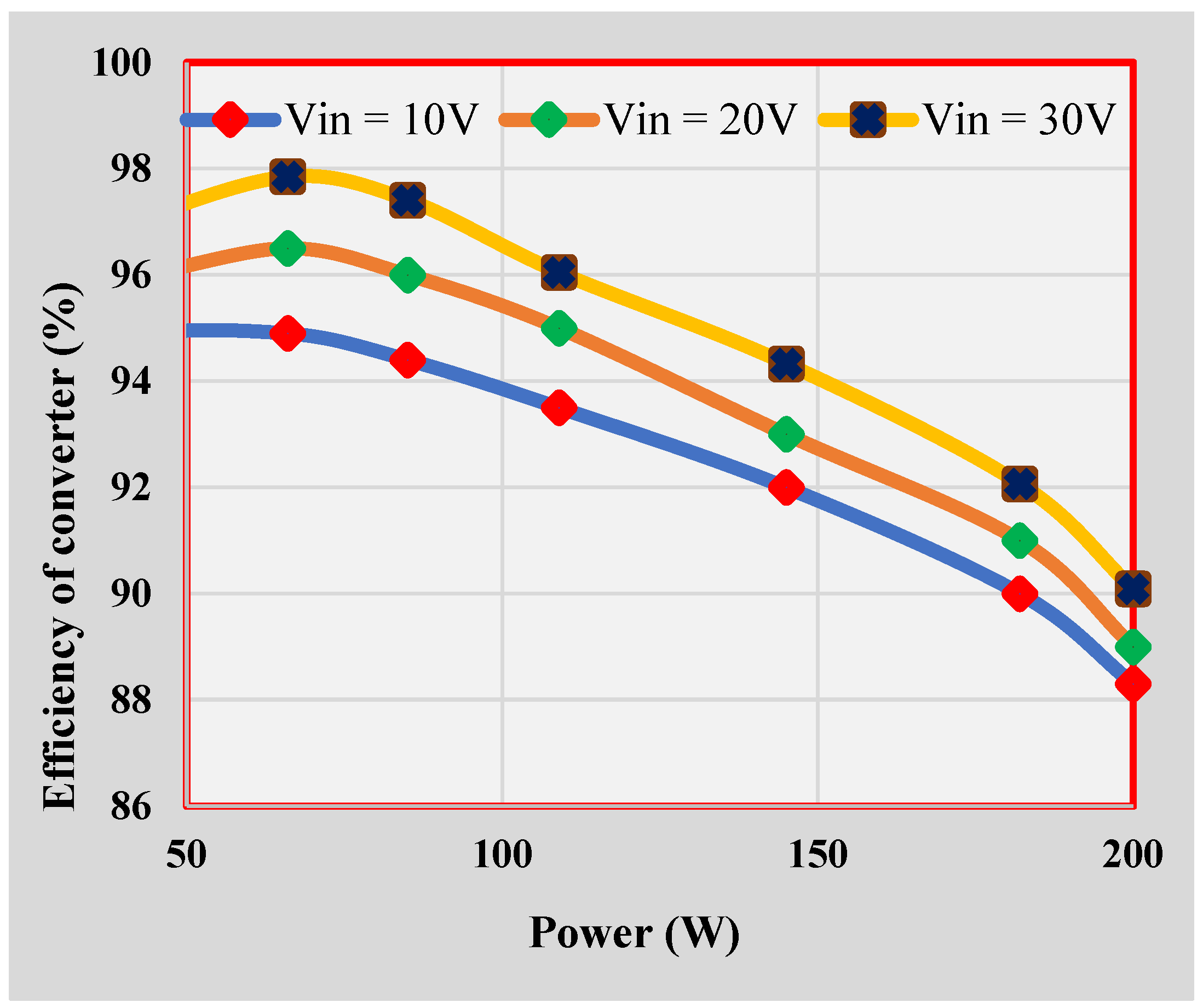
Figure 31 shows the variation in efficiency with the output power as the input voltage is increased. It can be observed that as the input voltage increases, the efficiency of the converter increases. This occurs because with the increase in voltage, the current decreases to conserve the power; hence, the conduction losses across various elements of the converter including switches, diodes, and parasitic resistances of the inductor and capacitor are reduced.
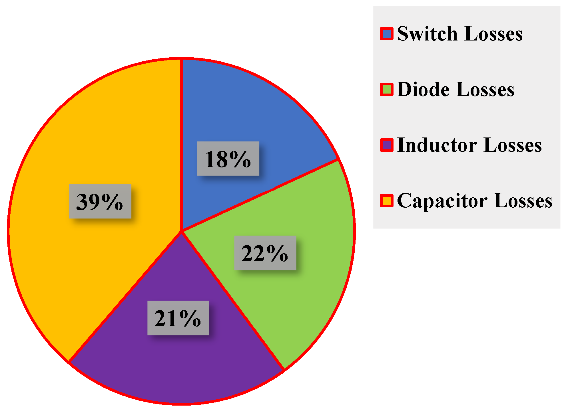
The maximum efficiency of the converter is found as 97.85% at 30 V, 66 W followed by 96.5% for operation at 20 V for the same power. From Figure 32, the majority of the conduction losses i.e., around 39%, occur in the capacitors, out of which 58.5% of the losses in capacitors are due to capacitor C3 itself. The switches and diodes contribute 40% of the total losses. The losses can be further reduced by using diodes and switches with low parasitic resistance.
6. Conclusions
The converter produces an ideal voltage gain of 11 times at a duty ratio of 30% with an ideal voltage gain of 14.44 at a duty ratio of 40%. The nonideal gain of the proposed converter at a D less than 60% is still found to be higher as compared to the ideal gains of the compared converters. In addition, the voltage stress across the switches is found to be lower than the output voltage and is also much lower than the compared topologies even at higher duty ratios. The voltage stress across S1 is 6.92% of the Vo and across switch S2, it is 46.15% of Vo at the duty ratio of 40%. The maximum efficiency of 97.85% is obtained at 66 W when the input voltage is 30 V, while it is 96.44% at a load of 38 W, keeping the input voltage at 20 V. The efficiency of the prototype model decreases with the power level due to the absence of galvanic isolation and parasitic resistances. The voltage and current stresses across the elements are low, which can be observed from the analysis and the hardware results. The converter has a common ground and operates at continuous input current, making it feasible for low- and medium-power solar and renewable energy PV applications.
Author Contributions
Conceptualization, writing—original draft preparation, M.Z., I.H.M. and M.T.; supervision, M.Z. and I.A.; writing—review and editing, B.A. and E.M.G.R.; funding acquisition, M.T., B.A. and E.M.G.R. All authors have read and agreed to the published version of the manuscript.
Funding
The authors would like to acknowledge the financial support from Taif University Researchers Supporting Project Number (TURSP-2020/278), Taif University, Taif, Saudi Arabia and from the collaborative research grant scheme (CRGS) project, Hardware-In-the-Loop (HIL) Lab, Department of Electrical Engineering, Aligarh Muslim University, India having project numbers CRGS/MOHD TARIQ/01 and CRGS/MOHD TARIQ/02.
Acknowledgments
The authors also acknowledge the support provided by the Hardware-In-the-Loop (HIL) Lab and Non-Conventional Energy (NCE) Lab, Department of Electrical Engineering, Aligarh Muslim University, India.
Conflicts of Interest
The authors declare no conflict of interest.
References
- Forouzesh, M.; Siwakoti, Y.; Gorji, S.; Blaabjerg, F.; Lehman, B. Step-Up DC–DC Converters: A Comprehensive Review of Voltage-Boosting Techniques, Topologies, and Applications. IEEE Trans. Power Electron. 2017, 32, 9143–9178. [Google Scholar] [CrossRef]
- Goyal, V.K.; Shukla, A. Isolated DC–DC Boost Converter for Wide Input Voltage Range and Wide Load Range Applications. IEEE Trans. Ind. Electron. 2021, 68, 9527–9539. [Google Scholar] [CrossRef]
- Ayachit, A.; Reatti, A.; Kazimierczuk, M.K. Magnetising inductance of multiple-output flyback dc–dc convertor for discontinuous conduction mode. IET Power Electron. 2017, 10, 451–461. [Google Scholar] [CrossRef] [Green Version]
- Hu, R.; Zeng, J.; Liu, J.; Guo, Z.; Yang, N. An Ultrahigh Step-Up Quadratic Boost Converter Based on Coupled-Inductor. IEEE Trans. Power Electron. 2020, 35, 13200–13209. [Google Scholar] [CrossRef]
- Lee, S.; Do, H. Quadratic Boost DC–DC Converter with High Voltage Gain and Reduced Voltage Stresses. IEEE Trans. Power Electron. 2019, 34, 2397–2404. [Google Scholar] [CrossRef]
- Das, P.; Mousavi, S.A.; Moschopoulos, G. Analysis and Design of a Nonisolated Bidirectional ZVS-PWM DC–DC Converter with Coupled Inductors. IEEE Trans. Power Electron. 2010, 25, 2630–2641. [Google Scholar] [CrossRef]
- Da Cunha Duarte, C.; Barbi, I. A new family of ZVS-PWM active-clamping DC-to-DC boost converters: Analysis, design, and experimentation. IEEE Trans. Power Electron. 1997, 12, 824–831. [Google Scholar] [CrossRef]
- Vinnikov, D.; Roasto, I.; Strzelecki, R.; Adamowicz, M. Step-up dc/dc converter switch cascaded quasi Z-source network. IEEE Trans. Ind. Electron. 2012, 59, 3727–3736. [Google Scholar] [CrossRef]
- Liu, J.; Wu, J.; Qiu, J.; Jun, Z. Switched Z-Source/Quasi-Z-Source DC–DC Converters with Reduced Passive Components for Photovoltaic Systems. IEEE Access 2019, 7, 40893–40903. [Google Scholar] [CrossRef]
- Haji-Esmaeili, M.; Babaei, E.; Sabahi, M. High Step-Up Quasi-Z Source DC–DC Converter. IEEE Trans. Power Electron. 2018, 33, 10563–10571. [Google Scholar] [CrossRef]
- Shen, H.; Zhang, B.; Qiu, D. Hybrid Z-Source Boost DC–DC Converters. IEEE Trans. Ind. Electron. 2017, 64, 310–319. [Google Scholar] [CrossRef]
- Karthikeyan, V.; Kumaravel, S.; Gurukumar, G. High step-up gain DC–DC converter with switched capacitor and regenerative boost configuration for solar PV applications. IEEE Trans. Circuits Syst. II Express Briefs 2019, 66, 2022–2026. [Google Scholar] [CrossRef]
- Tang, Y.; Fu, D.; Wang, T.; Xu, Z. Hybrid Switched-Inductor Converters for High Step-Up Conversion. IEEE Trans. Ind. Electron. 2015, 62, 1480–1490. [Google Scholar] [CrossRef]
- Samiullah, M.; Iqbal, A.; Ashraf, I.; Maroti, P. Voltage Lift Switched Inductor Double Leg Converter with Extended Duty Ratio for DC Microgrid Application. IEEE Access 2021, 9, 85310–85325. [Google Scholar] [CrossRef]
- Bhaskar, M.S.; Meraj, M.; Iqbal, A.; Padmanaban, S.; Maroti, P.K.; Alammari, R. High gain transformer-less double-duty-triple mode DC/DC converter for DC microgrid. IEEE Access 2019, 7, 36353–36370. [Google Scholar] [CrossRef]
- Zaid, M.; Khan, S.; Siddique, M.D.; Sarwar, A.; Ahmad, J.; Sarwer, Z.; Iqbal, A. A transformerless high gain dc–dc boost converter with reduced voltage stress. Int. Trans. Electr. Energy Syst. 2021, 31, e12877. [Google Scholar] [CrossRef]
- Ahmad, J.; Siddique, M.; Sarwar, A.; Lin, C.; Iqbal, A. A high gain noninverting DC–DC converter with low voltage stress for industrial applications. Int. J. Circuit Theory Appl. 2021, 49, 4212–4230. [Google Scholar] [CrossRef]
- Saravanan, S.; Babu, N. Design and Development of Single Switch High Step-Up DC–DC Converter. IEEE J. Emerg. Sel. Top. Power Electron. 2018, 6, 855–863. [Google Scholar] [CrossRef]
- Khan, S.; Zaid, M.; Mahmood, A.; Nooruddin, A.S.; Ahmad, J.; Alghaythi, M.L.; Alamri, B.; Tariq, M.; Sarwar, A.; Lin, C.H. A New Transformerless Ultra High Gain DC–DC Converter for DC Microgrid Application. IEEE Access 2021, 9, 124560–124582. [Google Scholar] [CrossRef]
- Andrade, A.; Faistel, T.; Toebe, A.; Guisso, R. Family of Transformerless Active Switched Inductor and Switched Capacitor Ćuk DC–DC Converter for High Voltage Gain Applications. IEEE J. Emerg. Sel. Top. Ind. Electron. 2021, 2, 390–398. [Google Scholar] [CrossRef]
- Sarikhani, A.; Allahverdinejad, B.; Hamzeh, M. A Nonisolated Buck–Boost DC–DC Converter with Continuous Input Current for Photovoltaic Applications. IEEE J. Emerg. Sel. Top. Power Electron. 2021, 9, 804–811. [Google Scholar] [CrossRef]
- Babaei, E.; MashinchiMaheri, H.; Sabahi, M.; Hosseini, S. Extendable Nonisolated High Gain DC–DC Converter Based on Active–Passive Inductor Cells. IEEE Trans. Ind. Electron. 2018, 65, 9478–9487. [Google Scholar] [CrossRef]
- Shahir, F.M.; Babaei, E.; Farsadi, M. Extended topology for a boost DC–DC converter. IEEE Trans. Power Electron. 2019, 34, 2375–2384. [Google Scholar] [CrossRef]
- Li, G. A Novel Quadratic Boost Converter with Low Inductor Currents. CPSS Trans. Power Electron. Appl. 2020, 5, 1–10. [Google Scholar] [CrossRef]
- Yang, P.; Xu, J.; Zhou, G.; Zhang, S. A new quadratic boost converter with high voltage step-up ratio and reduced voltage stress. In Proceedings of the 7th International Power Electronics and Motion Control Conference, Harbin, China, 2–5 June 2012. [Google Scholar] [CrossRef]
- Ahmad, J.; Zaid, M.; Sarwar, A.; Tariq, M.; Sarwer, Z. A New Transformerless Quadratic Boost Converter with High Voltage Gain. Smart Sci. 2020, 8, 163–183. [Google Scholar] [CrossRef]
- Varesi, K.; Esfahlan, A.G. An Enhanced-Gain Quadratic-Boost DC–DC Configuration. In Proceedings of the 2020 28th Iranian Conference on Electrical Engineering (ICEE), Tabriz, Iran, 4–6 August 2020; pp. 1–5. [Google Scholar] [CrossRef]
- Mahmood, A.; Zaid, M.; Ahmad, J.; Khan, M.A.; Khan, S.; Sifat, Z.; Lin, C.H.; Sarwar, A.; Tariq, M.; Alamri, B. A Non-Inverting High Gain DC–DC Converter with Continuous Input Current. IEEE Access 2021, 9, 54710–54721. [Google Scholar] [CrossRef]
- Rahimi, T.; Ding, L.; Gholizadeh, H.; Shahrivar, R.S.; Faraji, R. An Ultra High Step-Up DC–DC Converter Based on the Boost, Luo, and Voltage Doubler Structure: Mathematical Expression, Simulation, and Experimental. IEEE Access 2021, 9, 132011–132024. [Google Scholar] [CrossRef]
- Varesi, K.; Hassanpour, N.; Saeidabadi, S. Novel high step-up DC–DC converter with increased voltage gain per devices and continuous input current suitable for DC microgrid applications. Int. J. Circ. Theor. Appl. 2020, 48, 1820. [Google Scholar] [CrossRef]
Figure 1.
A traditional quadratic boost converter (TQBC).

Figure 2.
Converter proposed in [19].
Figure 2.
Converter proposed in [19].

Figure 3.
Proposed high-gain dc–dc converter topology.

Figure 4.
Conduction diagram of the converter in ON-state (Mode 1).

Figure 5.
Conduction diagram of the proposed converter in OFF state (Mode 2).

Figure 6.
Inductor voltages.

Figure 7.
Switch voltages.

Figure 8.
Diode voltages.

Figure 9.
Diode voltages.

Figure 10.
Switch currents.

Figure 11.
Inductor currents.

Figure 12.
Typical waveforms during DCM.

Figure 13.
Boundary normalized inductor time constant versus the duty ratio.

Figure 14.
Nonideal realization of the proposed topology.

Figure 15.
Comparison of calculated ideal and simulated nonideal voltage gain of the proposed converter.
Figure 15.
Comparison of calculated ideal and simulated nonideal voltage gain of the proposed converter.

Figure 16.
Voltage gain variation as per parasitic resistance of the switch.

Figure 17.
Voltage gain variation as per parasitic resistance of the inductor.

Figure 18.
Voltage gain variation as per parasitic resistance of the capacitor.

Figure 19.
(a) Comparison of ideal voltage gain of various similar converters [4,5,16,22,24,25,26,27,28,29,30]. (b) Comparison of various topologies with the nonideal voltage gain of proposed topology [4,24,27,28].

Figure 20.
Comparison of calculated switch stress versus voltage gain [4,5,16,22,24,25,26,27,28,29].

Figure 21.
Simulated output voltage (), input voltage ( ), and duty cycle (D).

Figure 22.
Simulated inductor currents ( and duty cycle (D).

Figure 23.
Simulated switch voltages and duty cycle (D).

Figure 24.
Simulated capacitor voltages and duty cycle (D).

Figure 25.
Simulated capacitor voltages and duty cycle (D).

Figure 26.
Top to bottom: experimental waveforms of output voltage , input voltage , and at D = 0.4.
Figure 26.
Top to bottom: experimental waveforms of output voltage , input voltage , and at D = 0.4.

Figure 27.
Top to bottom: experimental waveforms of current of inductor L1 , inductor L2, and at D = 0.4.
Figure 27.
Top to bottom: experimental waveforms of current of inductor L1 , inductor L2, and at D = 0.4.

Figure 28.
Top to bottom: experimental waveforms of output voltage , voltage across switch S2 and at D = 0.4.
Figure 28.
Top to bottom: experimental waveforms of output voltage , voltage across switch S2 and at D = 0.4.

Figure 29.
Top to bottom: experimental waveforms of voltage across capacitor C3, the voltage across capacitor C4, and the voltage across capacitor C1 at D = 0.4.
Figure 29.
Top to bottom: experimental waveforms of voltage across capacitor C3, the voltage across capacitor C4, and the voltage across capacitor C1 at D = 0.4.

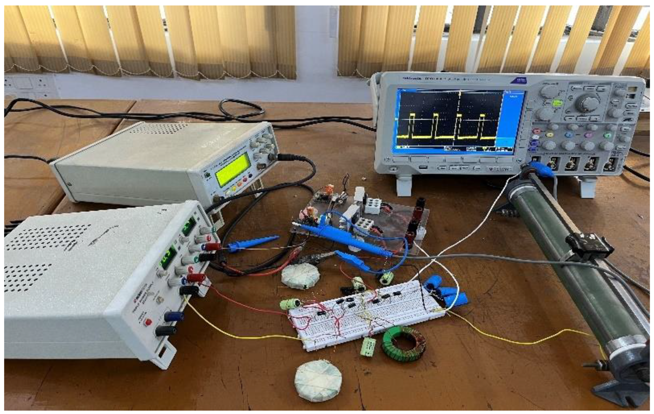
Figure 30.
Experimental Set-up.

Figure 31.
Simulated efficiency vs. output power comparison of the proposed converter at different input voltages.
Figure 31.
Simulated efficiency vs. output power comparison of the proposed converter at different input voltages.

Figure 32.
Distribution of losses across various elements of the converter.


Table 1.
Comparison of proposed topology with certain similar topologies.
| Topology | MCCM at D = 0.5 | Common Ground | ||||||
|---|---|---|---|---|---|---|---|---|
| Boost Converter | 1 | 1 | 1 | 1 | 2 | Yes | ||
| Quadratic Boost Converter | 2 | 2 | 1 | 3 | 4 | Yes | ||
| [4] | 1 + 1 coupled inductor | 5 | 2 | 5 | 14 | Yes | ||
| [5] | 1 + 1 coupled inductor | 3 | 1 | 5 | 6 | Yes | ||
| [16] | 3 | 4 | 2 | 5 | 11 | No | ||
| [22] | 8 | 1 | 4 | 17 | 9 | No | ||
| [24] | 2 | 2 | 2 | 2 | 4 | Yes | ||
| [25] | 3 | 4 | 1 | 4 | 6 | Yes | ||
| [26] | 3 | 3 | 1 | 5 | 8 | Yes | ||
| [27] | 3 | 5 | 2 | 4 | 10 | Yes | ||
| [28] | 2 | 5 | 1 | 6 | 12 | No | ||
| [29] | 3 | 6 | 1 | 6 | 10 | Yes | . | |
| [30] | 2 | 3 | 2 | 3 | 7 | Yes | ||
| Proposed Topology | 3 | 6 | 2 | 7 | 20 | Yes |
Table 2.
Hardware values of parameters.
| Parameter | Symbol | Value |
|---|---|---|
| Input Voltage | 20 V | |
| Duty Cycle | 0.4 | |
| Output Power | 67 W | |
| Load Resistance | 850 Ω | |
| Inductors | 330 μH, ESR = 0.12 Ω | |
| 0.4 mH ESR = 0.14 Ω | ||
| Capacitors | 47 μF, ESR = 0.1 Ω | |
| 100 μF, ESR = 0.22 Ω | ||
| Diodes | HER806 | |
| Power MOSFETs | SPW52N50C3 | |
| Driver | TLP250H | |
| Controller | STM32F334R8 | |
| Switching Frequency | 50 kHz |
Publisher’s Note: MDPI stays neutral with regard to jurisdictional claims in published maps and institutional affiliations. |
© 2022 by the authors. Licensee MDPI, Basel, Switzerland. This article is an open access article distributed under the terms and conditions of the Creative Commons Attribution (CC BY) license (https://creativecommons.org/licenses/by/4.0/).
Share and Cite
MDPI and ACS Style
Zaid, M.; Malick, I.H.; Ashraf, I.; Tariq, M.; Alamri, B.; Rodrigues, E.M.G. A Nonisolated Transformerless High-Gain DC–DC Converter for Renewable Energy Applications. Electronics 2022, 11, 2014. https://doi.org/10.3390/electronics11132014
AMA Style
Zaid M, Malick IH, Ashraf I, Tariq M, Alamri B, Rodrigues EMG. A Nonisolated Transformerless High-Gain DC–DC Converter for Renewable Energy Applications. Electronics. 2022; 11(13):2014. https://doi.org/10.3390/electronics11132014
Chicago/Turabian StyleZaid, Mohammad, Ifham H. Malick, Imtiaz Ashraf, Mohd Tariq, Basem Alamri, and Eduardo M. G. Rodrigues. 2022. "A Nonisolated Transformerless High-Gain DC–DC Converter for Renewable Energy Applications" Electronics 11, no. 13: 2014. https://doi.org/10.3390/electronics11132014
Note that from the first issue of 2016, this journal uses article numbers instead of page numbers. See further details here.