
Design and Fabrication of an Isolated Two-Stage AC–DC Power Supply with a 99.50% PF and ZVS for High-Power Density Industrial Applications


Abstract
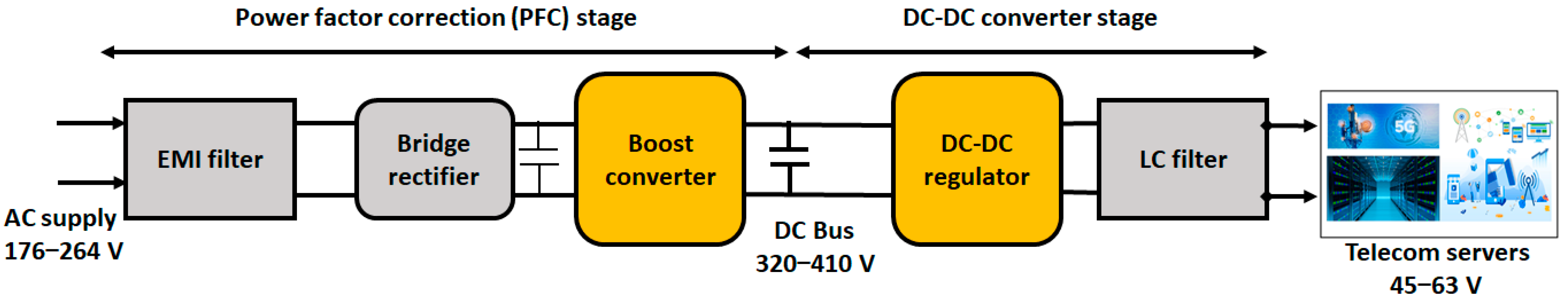
:1. Introduction
2. Power Factor Correction (PFC) Stage Design
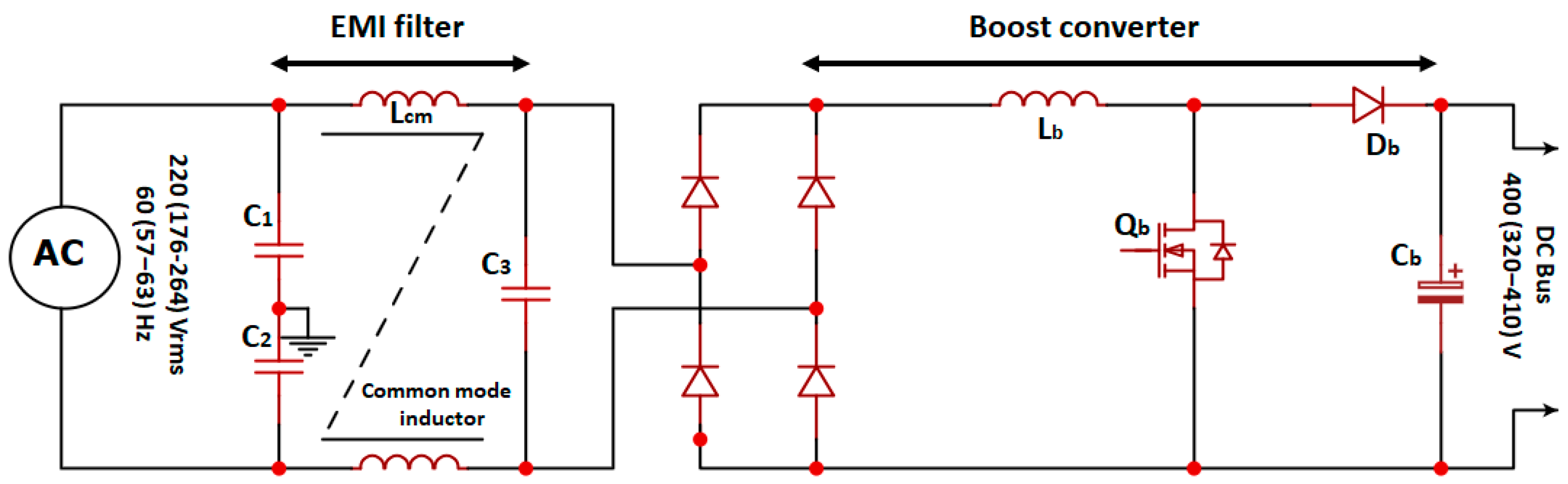
2.1. PFC Stage Power Components Design and Manufacturing
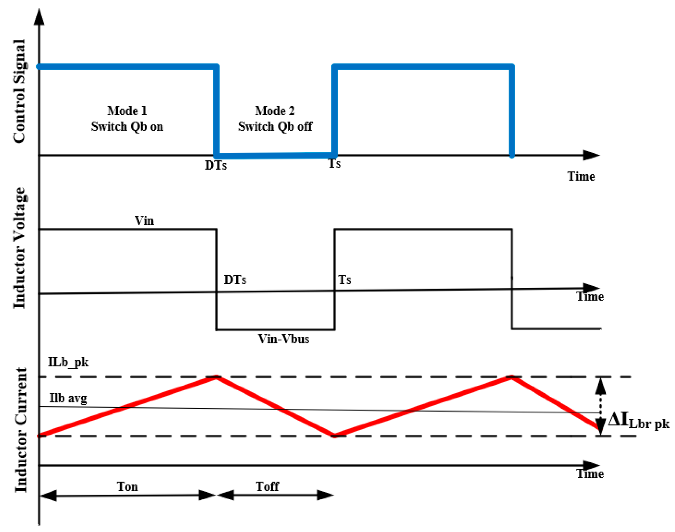
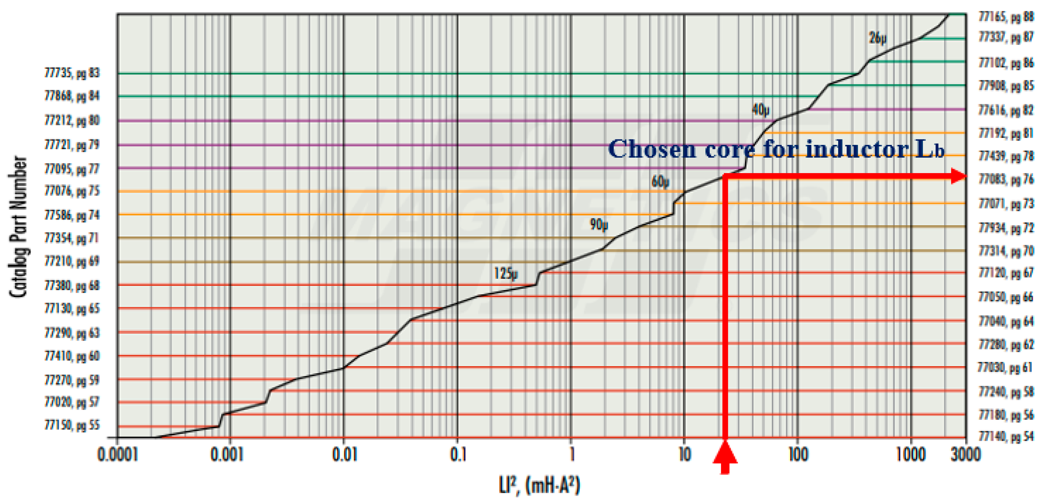
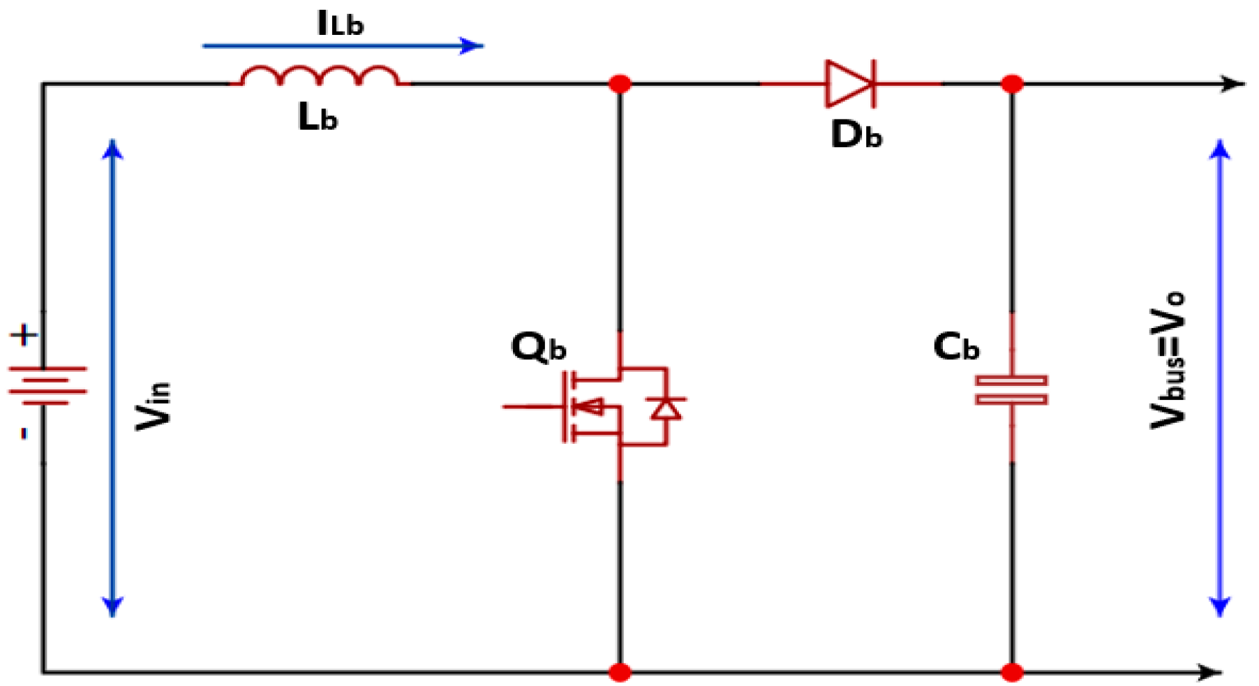
2.1.1. Boost Inductor
- 1.
- The required boost inductance value can be obtained on the basis of the required boost inductor input ripple current, which is commonly computed as a percentage (10–40%) of the maximum input current to the boost converter. As given in the design specifications in Table 1, for a 15% ripple current, the inductor ripple current can be calculated aswhere Iin max is the boost converter maximum input current and can be calculated aswhere Vin min is the minimum input voltage to the boost converter in V. η and PF are the target efficiency and power factor of the designed PFC stage, respectively.
- 2.
- To compute the average and maximum peak currents of the specified boost inductor, the boost converter used is assumed to work in the continuous current conduction mode (CCM), with two operation modes when the switch Qb is on and off. Figure 3 depicts the boost converter’s inductor voltage and current waveforms in various operation modes.

- 3.
- On the basis of the calculated inductance and the inductor maximum peak current, the inductor core part number, the number of turns (N), and the size of the winding wire have to be selected.
- 4.
- Power losses in the PFC boost inductors are caused by (i) the DCR resistance losses (PLb DCR) of the inductor wire and (2) the inductor core losses (PLb Core).
2.1.2. DC Bus Capacitor
2.1.3. Mosfet Switch
2.1.4. Boost Diode
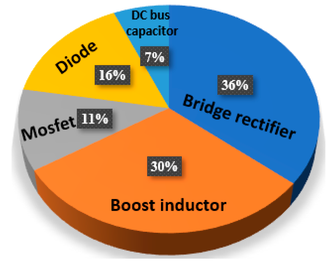
2.2. Power Loss Distribution in the PFC Stage
2.3. Boost Converter Average Small-Signal Model
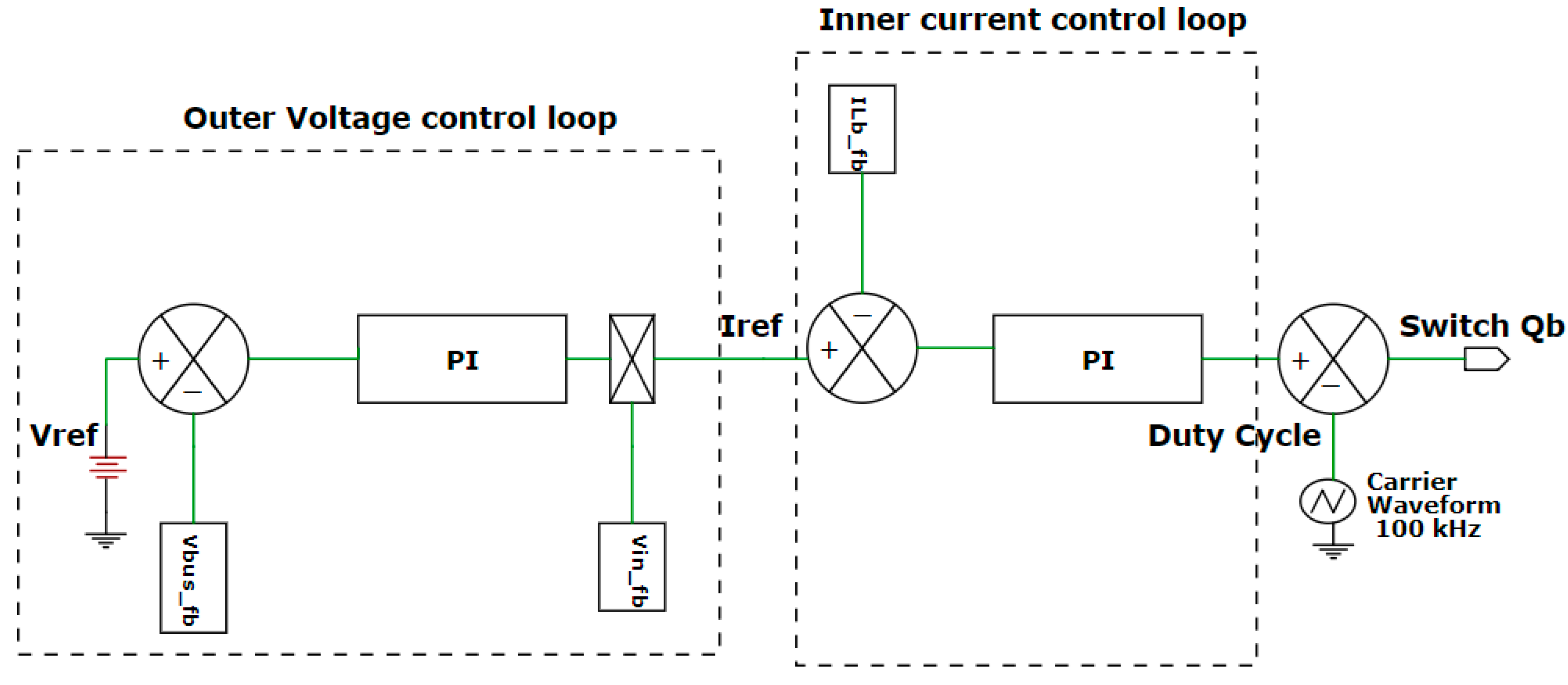
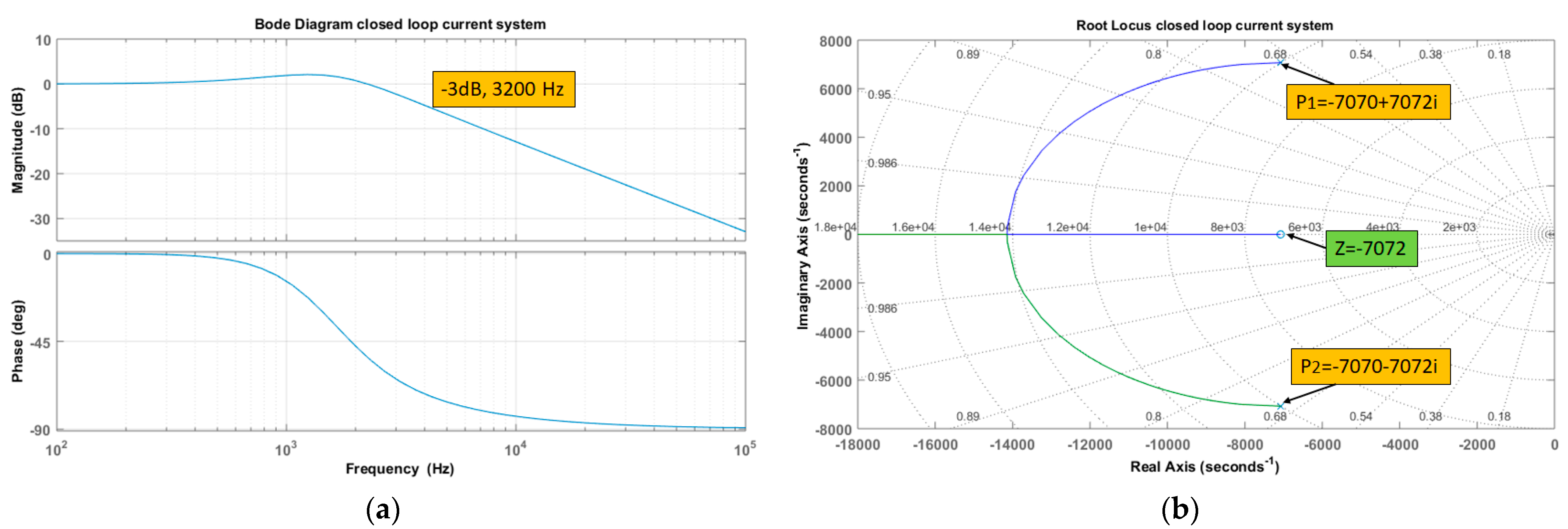
2.4. PFC Stage Control Circuit Design
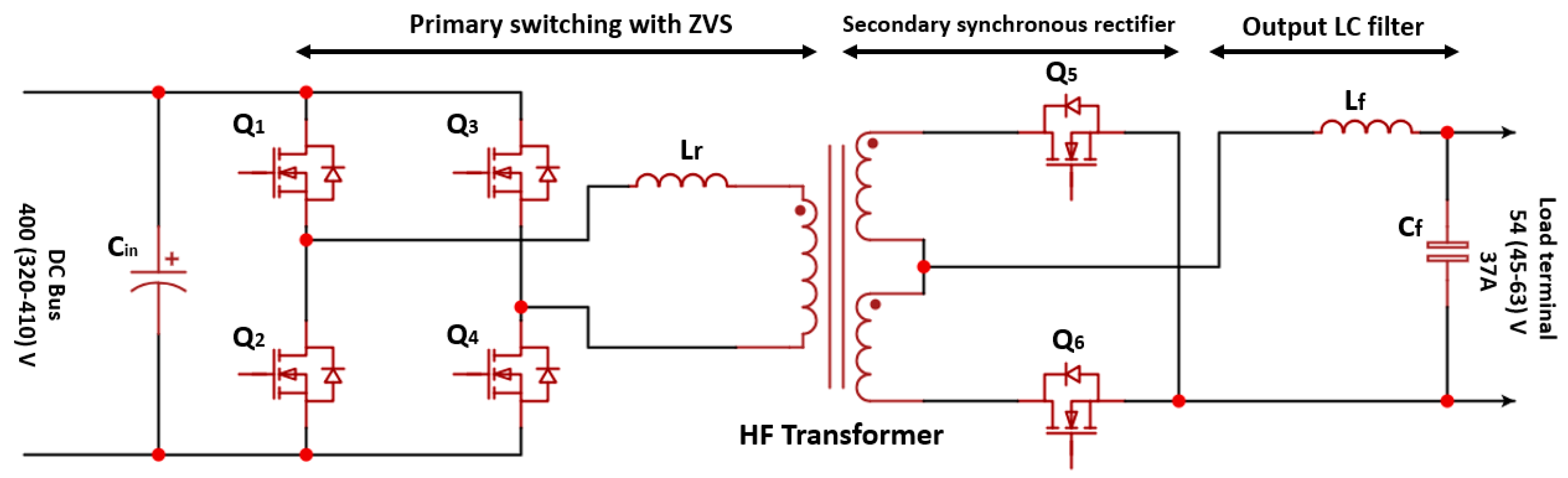
3. Phase-Shift PWM ZVS DC–DC Converter Stage Design
3.1. Phase-Shift PWM ZVS Converter Power Component Design and Manufacture
3.1.1. High-Frequency (HF) Transformer
- 1.
- The transformer turns ratio (a) is calculated on the basis of the maximum operating duty cycle (Dmax) at the minimum bus voltage rating of the converter (Vbus min), as follows:
- 2.
- The transformer magnetizing inductance (Lm) is designed based on the maximum magnetizing inductance to realize ZVS as given [33,36]where CHB denotes the entire equivalent capacitance of the primary H bridge, which can be found on the primary switch datasheet. Ts min is the minimum switching time, which is determined by the intended minimum switching frequency; Tdead is the PWM dead time, which may be computed using the effective duty ratio previously obtained.
- 3.
- When selecting the transformer core size, shape, and material, the main considerations are its efficiency, temperature rise, operating frequency, eddy currents, and core losses. For high-frequency applications (10 kHz–3 MHz), iron powder cores, amorphous steel cores, and ferrite cores can be used. However, ferrite cores serve as efficient insulators to prevent eddy currents and experience low core loss. When choosing the core, it is also possible to begin with a core weight (We), a core effective volume (Ve), or a core effective area (Ae) based on the transfer power and switching frequency and choose which core will be most appropriate in these terms.
- 4.
- Three main losses in the transformer have to be calculated: the core losses, the primary copper losses, and the secondary copper losses.
- For the ferrite cores, the transformer core losses can be calculated as [37]
- The primary winding RMS current and the copper losses due to the primary winding resistance (Rp) can be calculated as
- The secondary winding RMS current and the copper losses due to the secondary winding resistance (Rs) can be calculated as
3.1.2. Input Capacitor Design
3.1.3. Primary Mosfet Selection
- Low on-state resistance (Rdson) for low power losses.
- Fast turn-off switching and higher gate plateau voltage.
- Low gate charge Qg and low capacitance at the output Coss for designs with a wider ZVS range and less deadtime.
- High dVDS/dt and high dIF/dt to withstand spikes and overshoots.
- Low thermal resistance to decrease thermal power dissipation.
- Body diode with a high reverse recovery rate. The reverse recovery condition occurs when the body diode of a power Mosfet is switched from on-state to off-state while a current is flowing. The drain–source voltage rises rapidly as a result of this.
3.1.4. Secondary Mosfet Selection
3.1.5. Load Filter Inductor Design
3.1.6. Load Filter Capacitor Selection
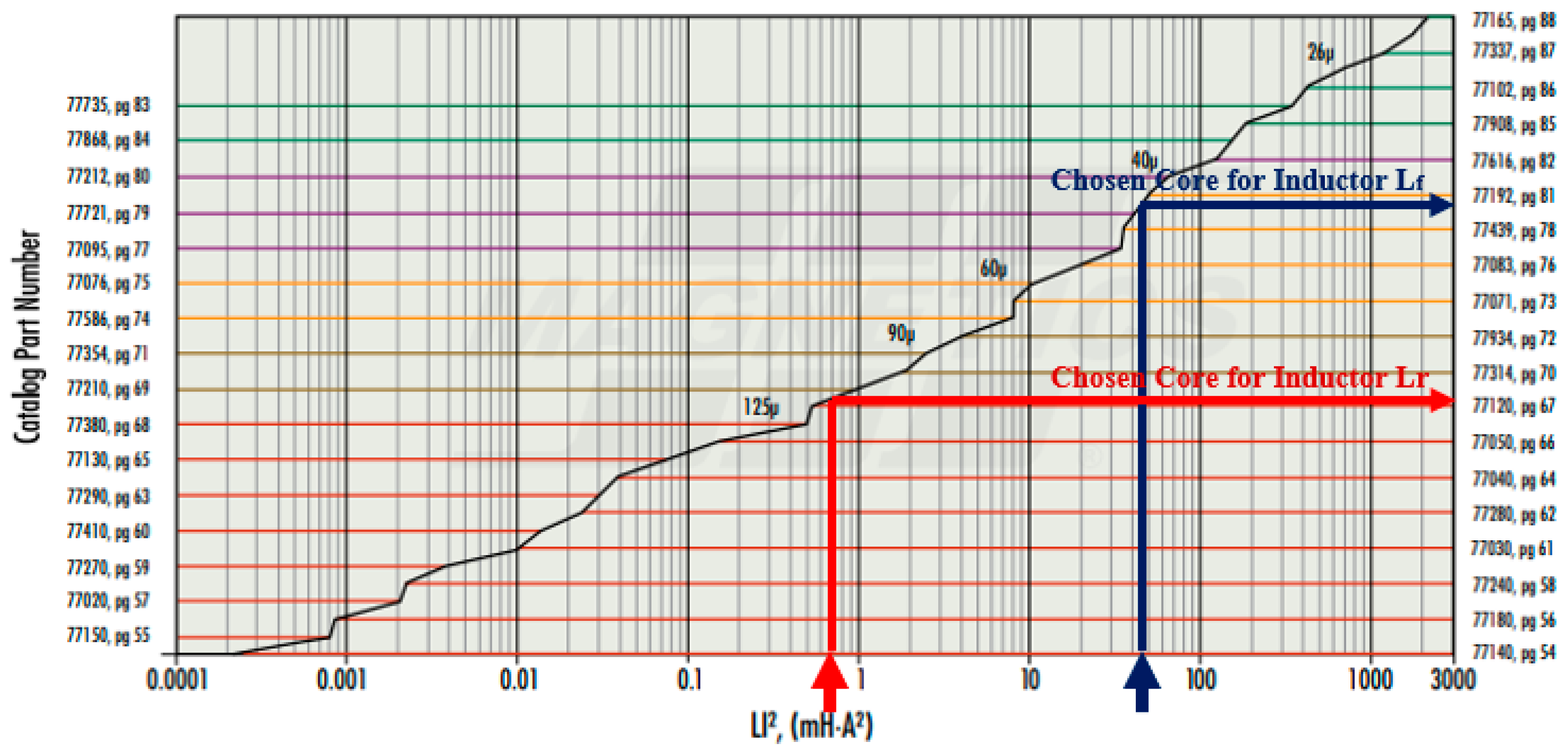
3.1.7. Resonant Inductor Design
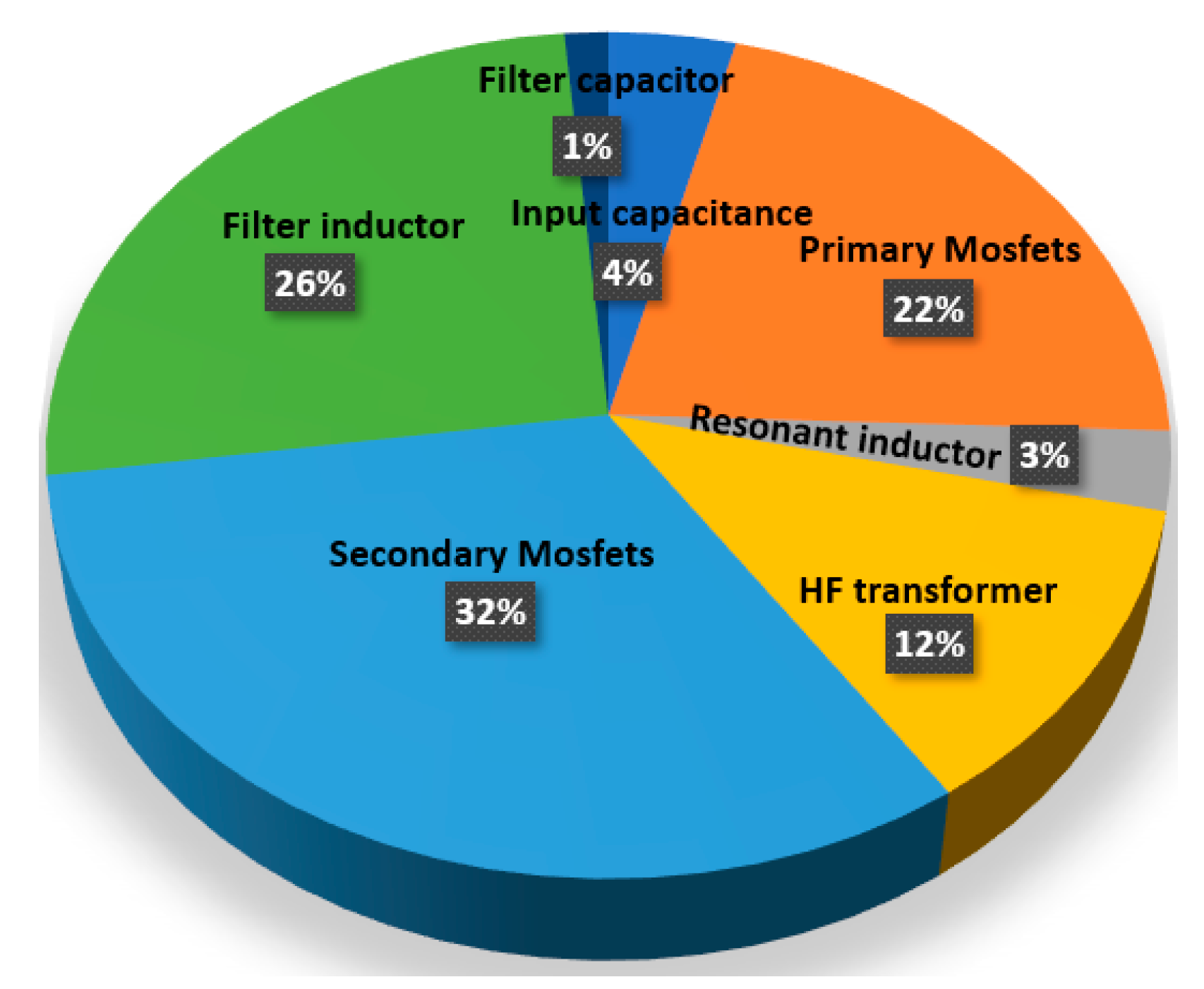
3.2. Power Loss Distribution in the DC–DC Converter Stage
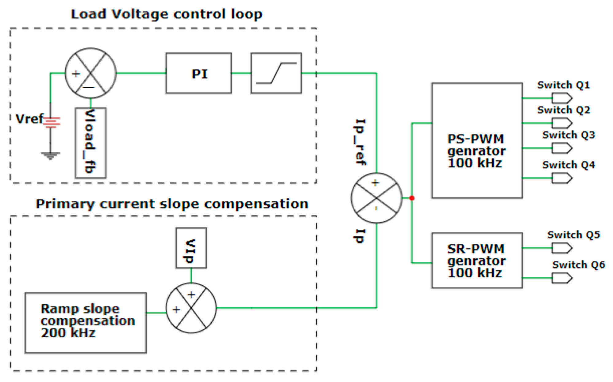
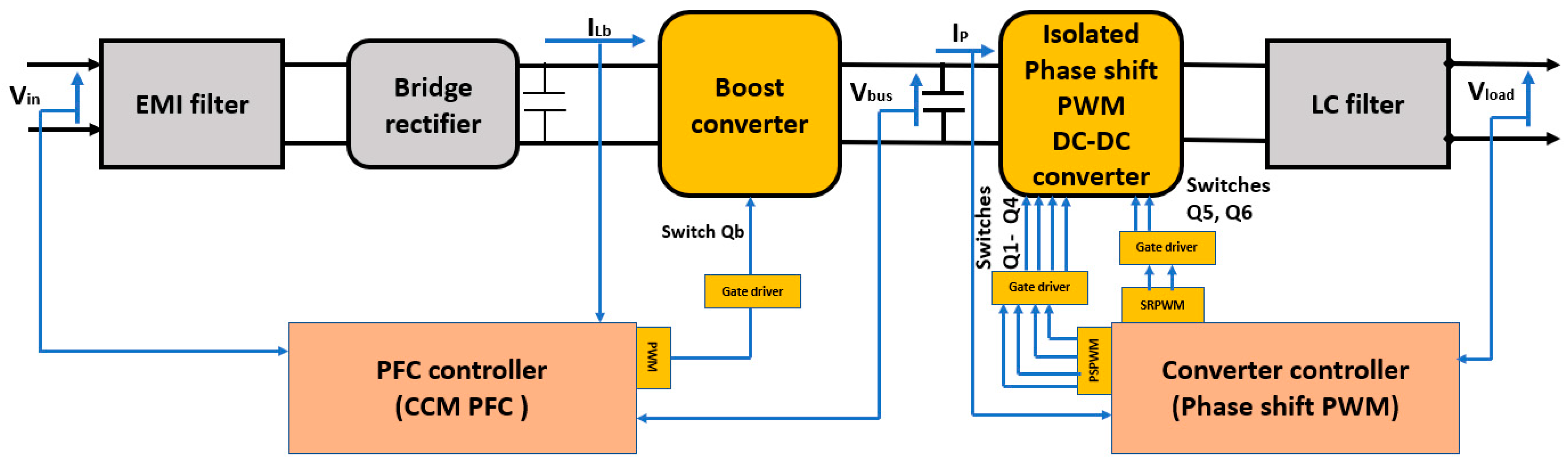
3.3. Control Circuit Implementation of the Phase-Shift PWM ZVS DC–DC Converter
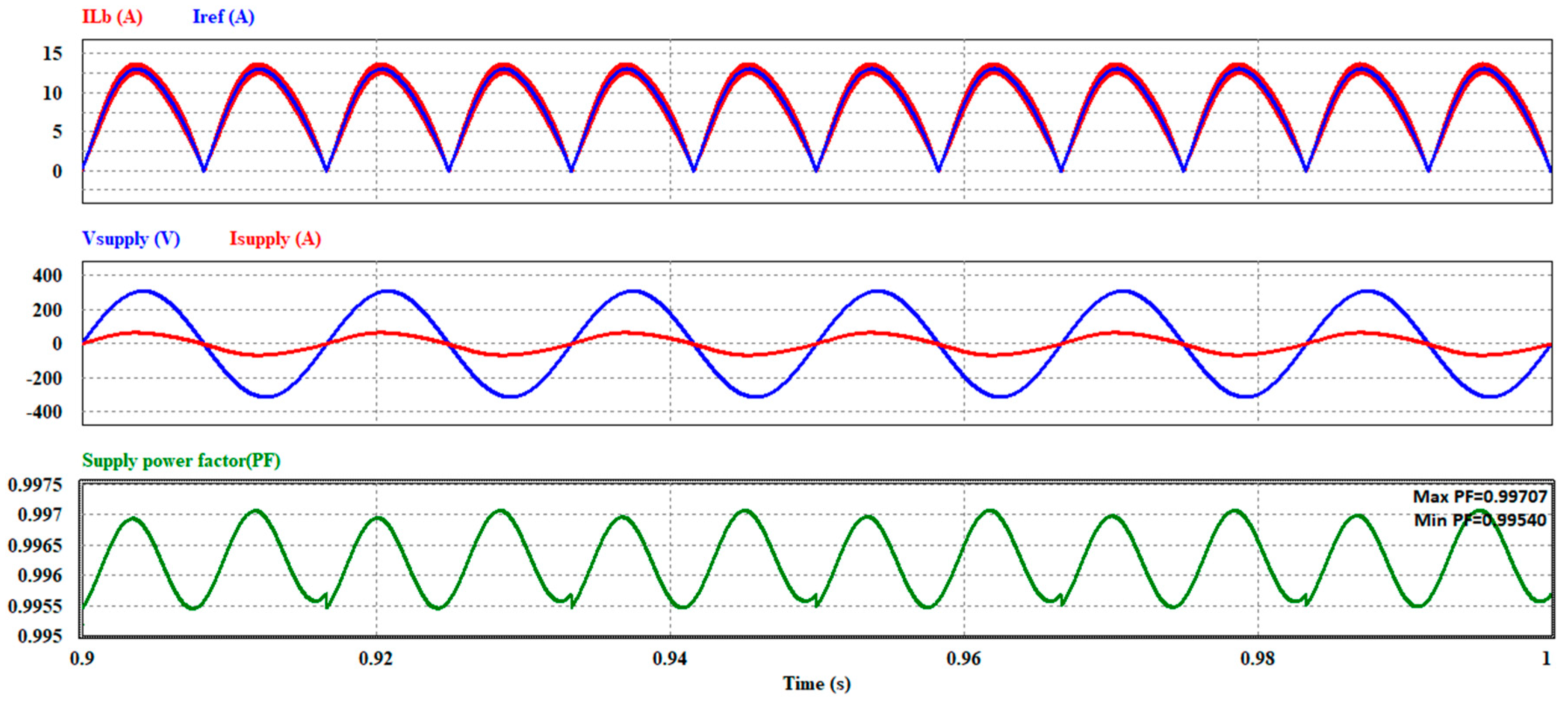
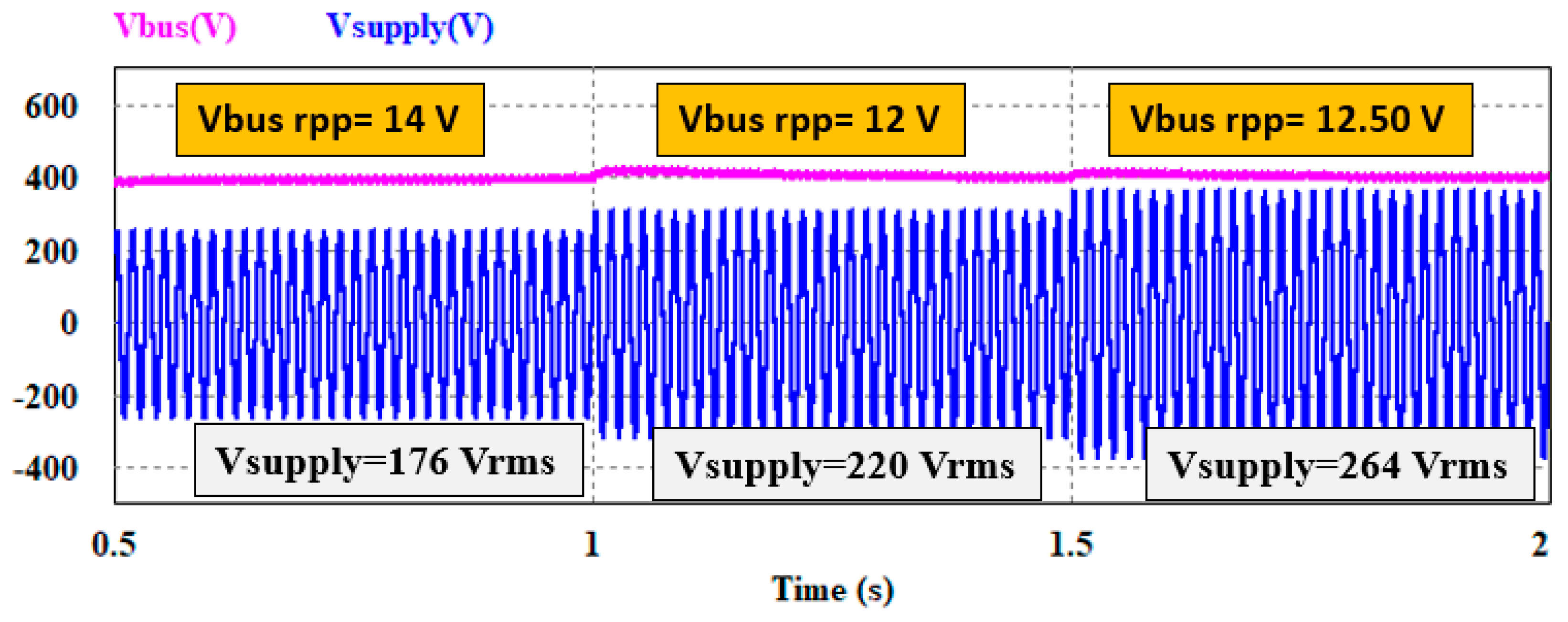
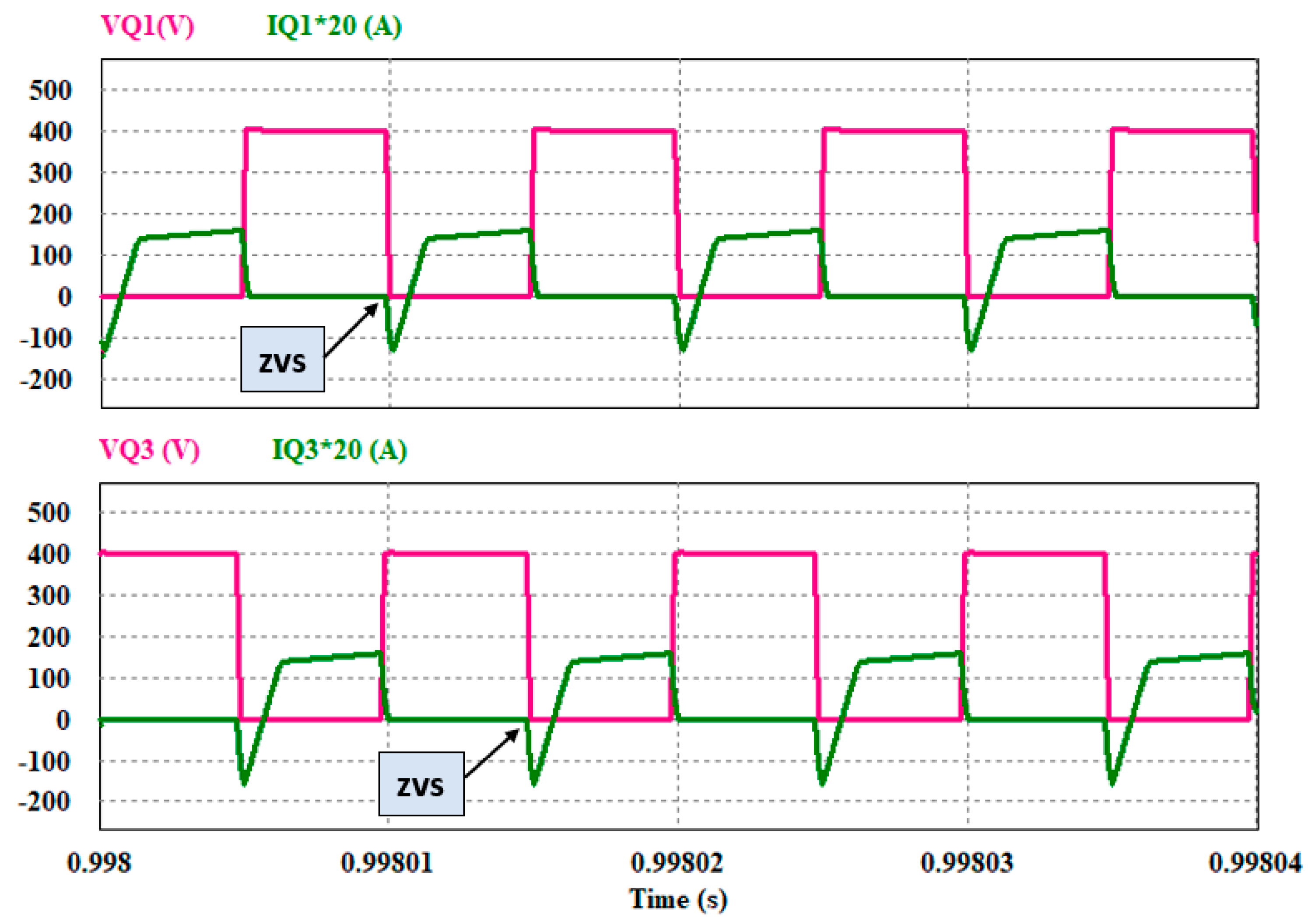
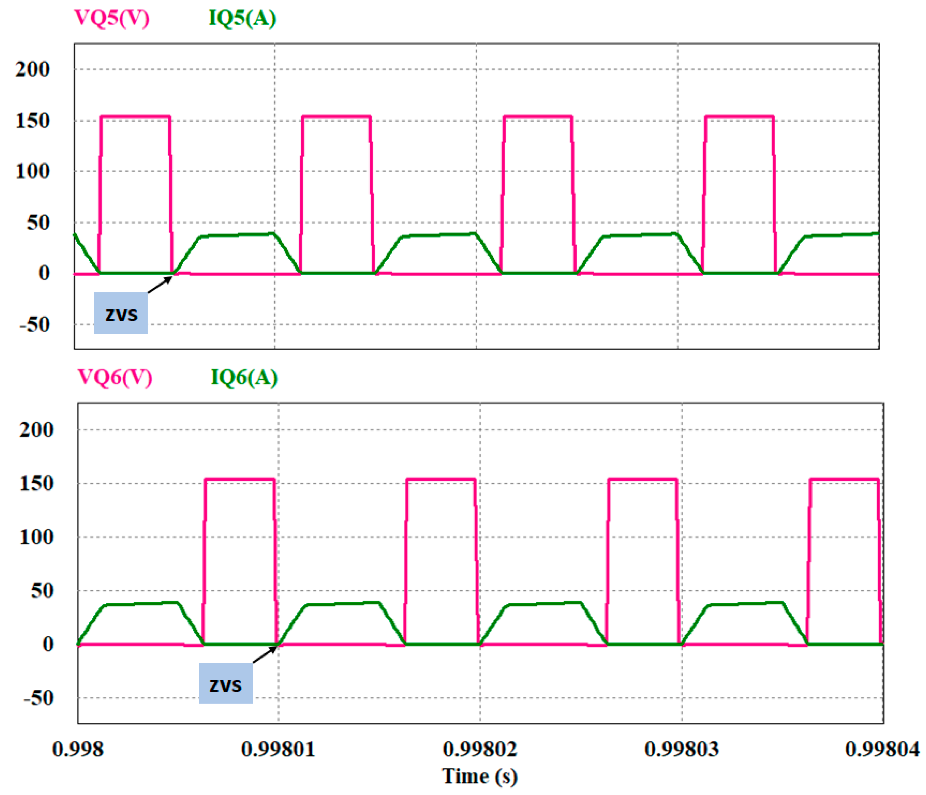
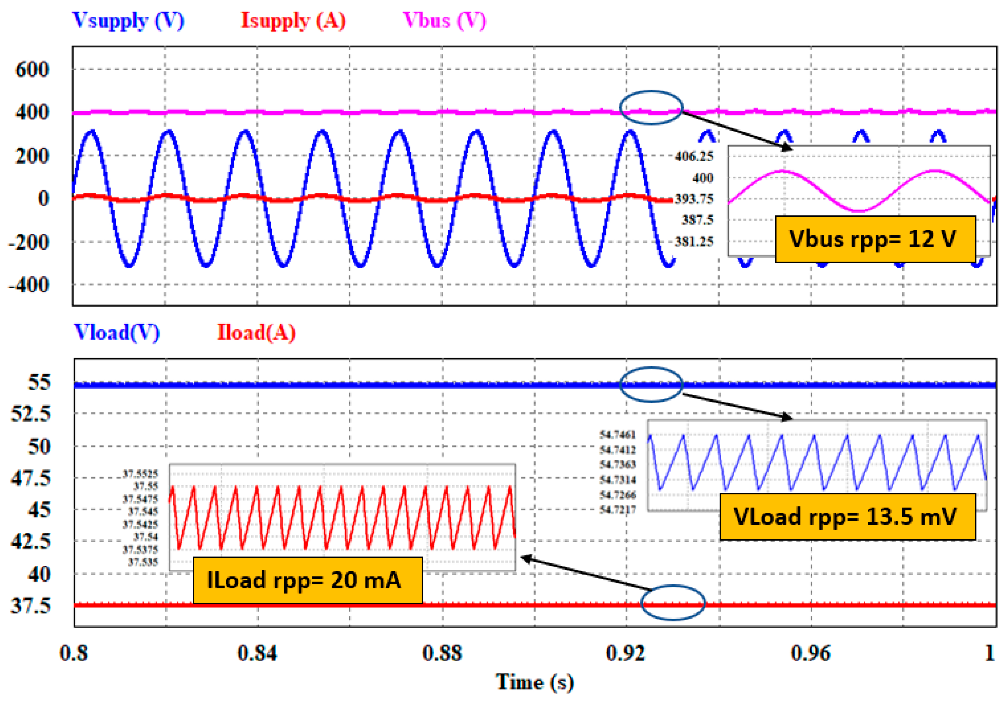
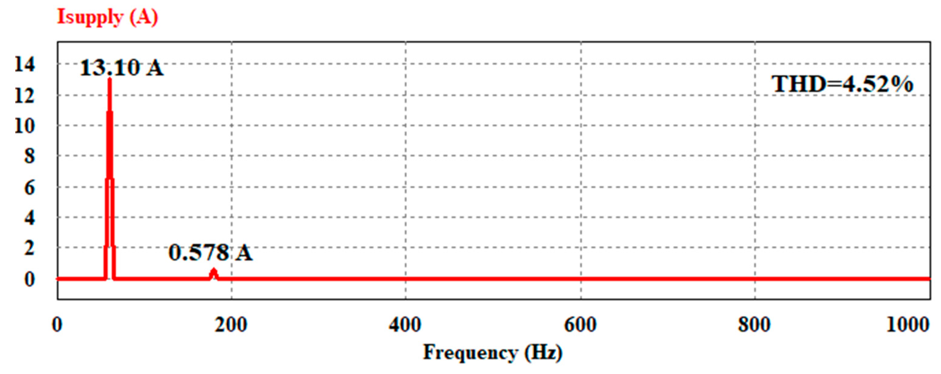
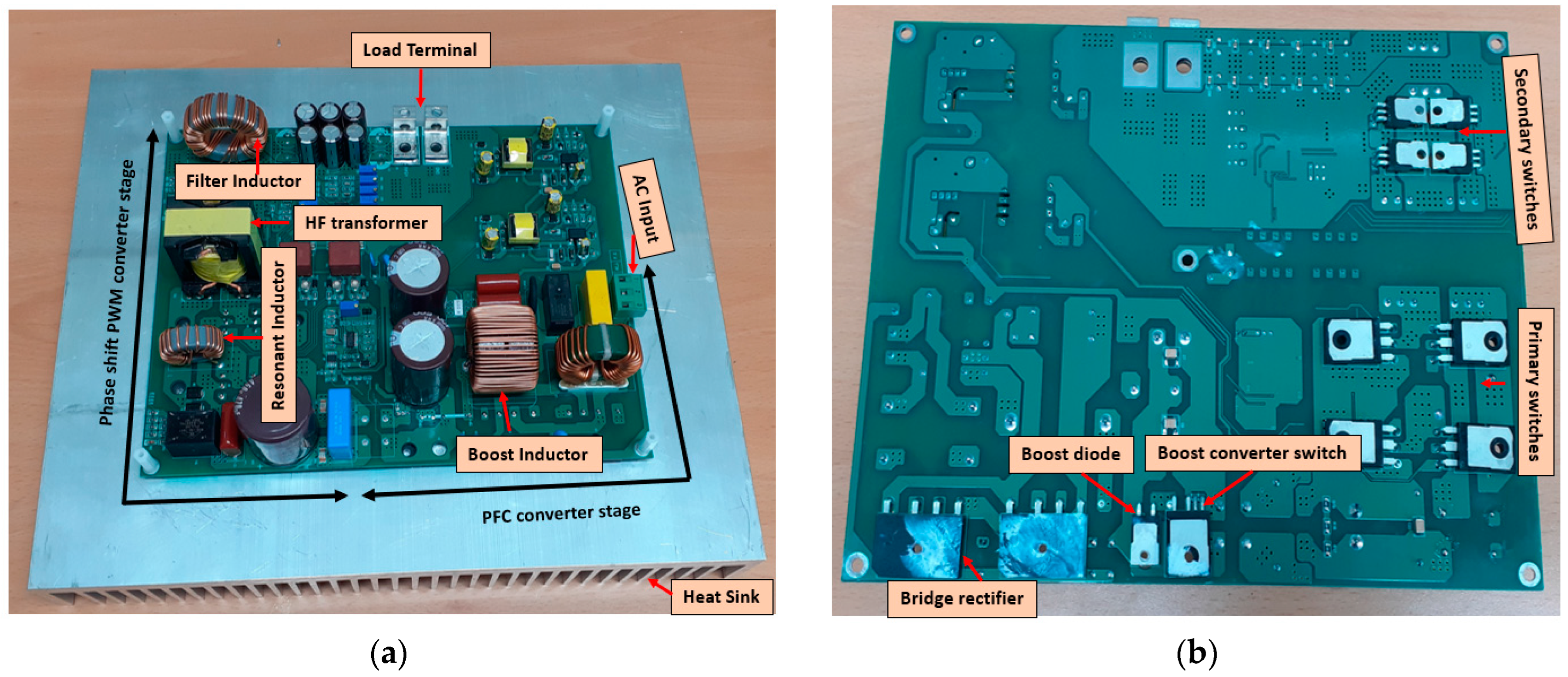
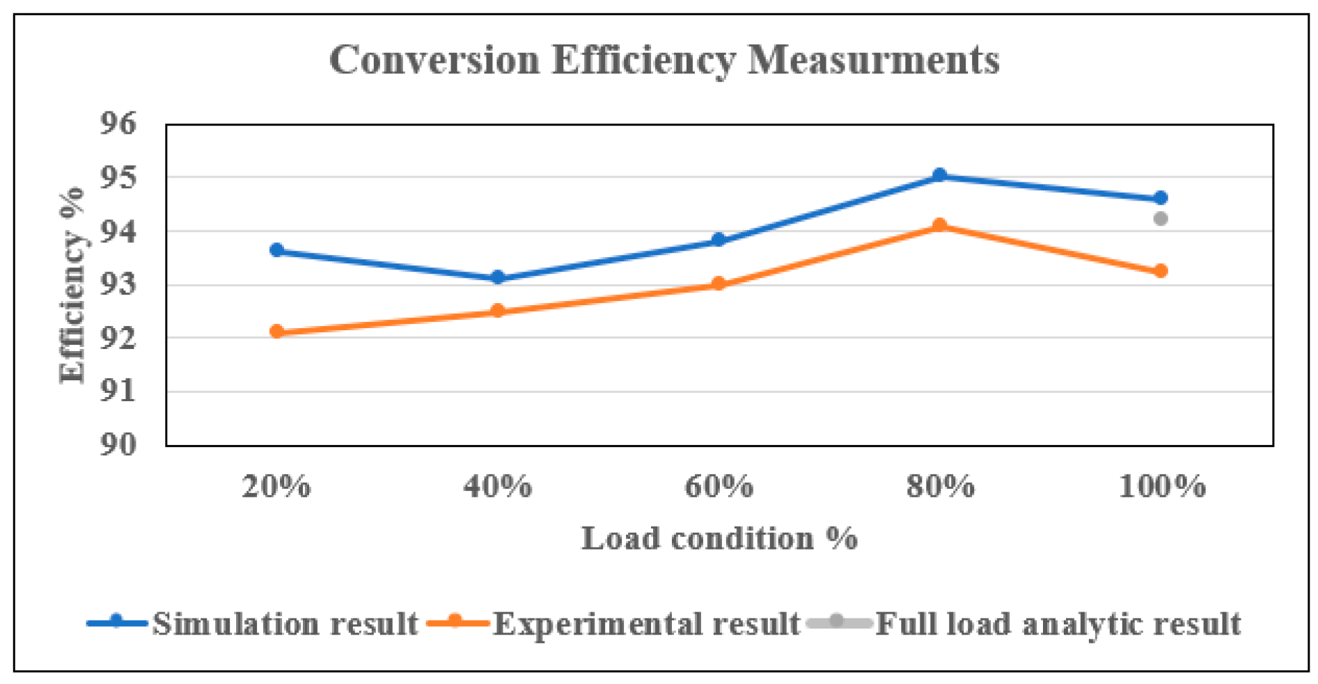
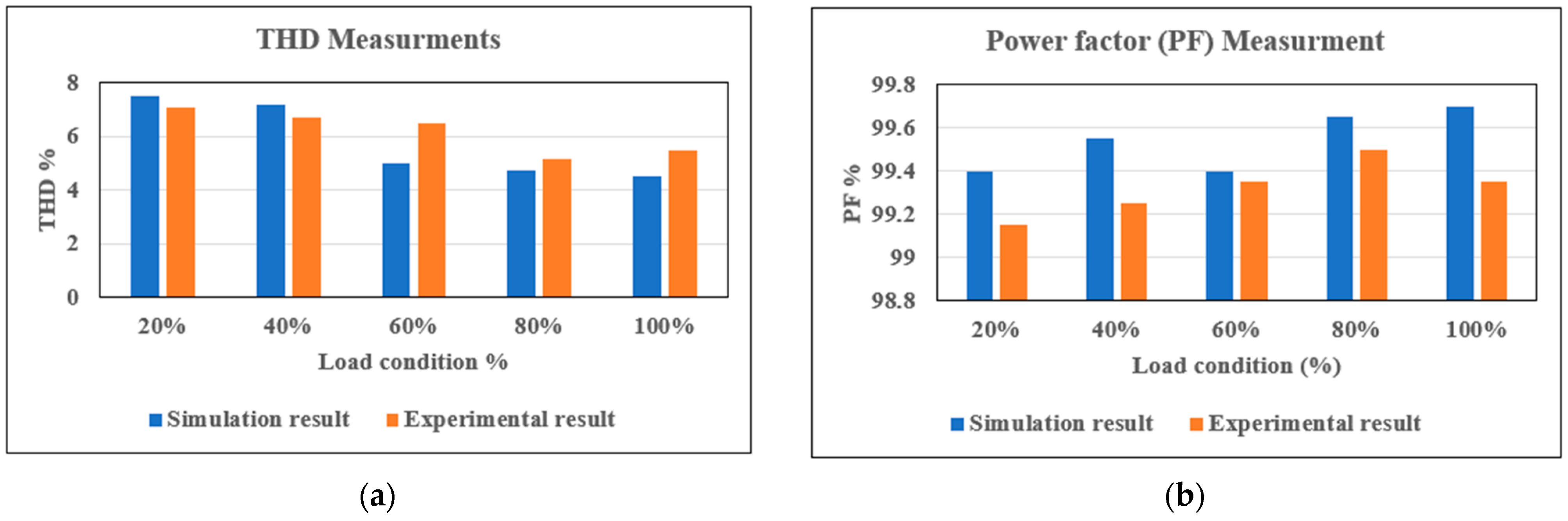
4. Simulation Results and Discussions
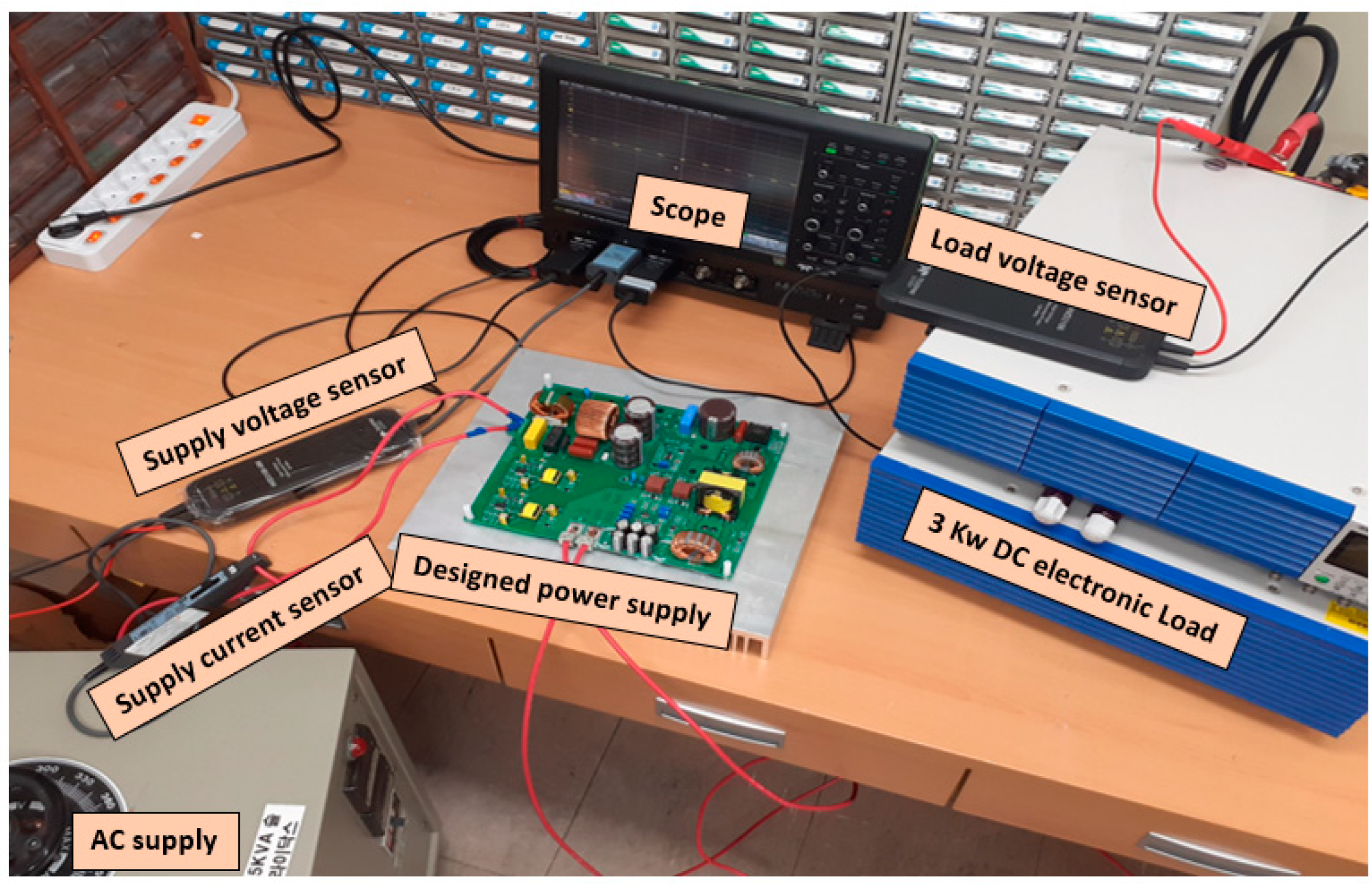
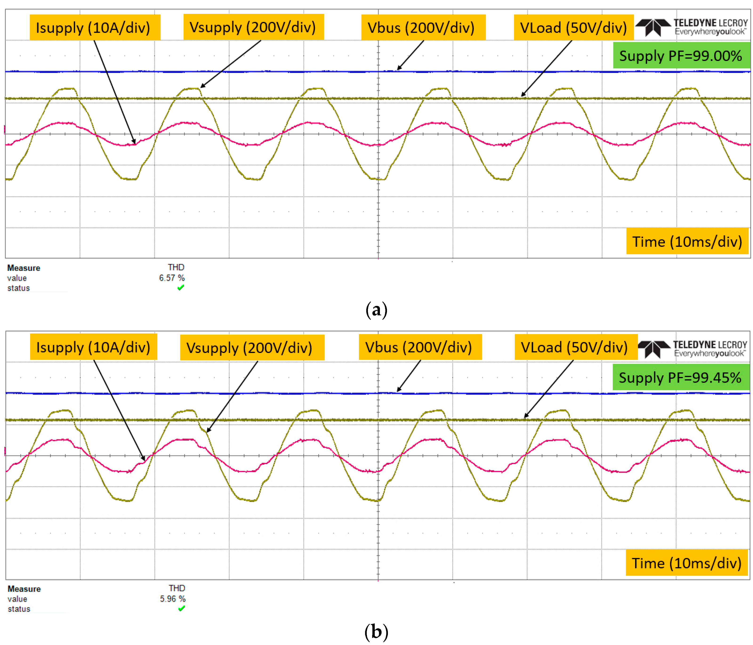
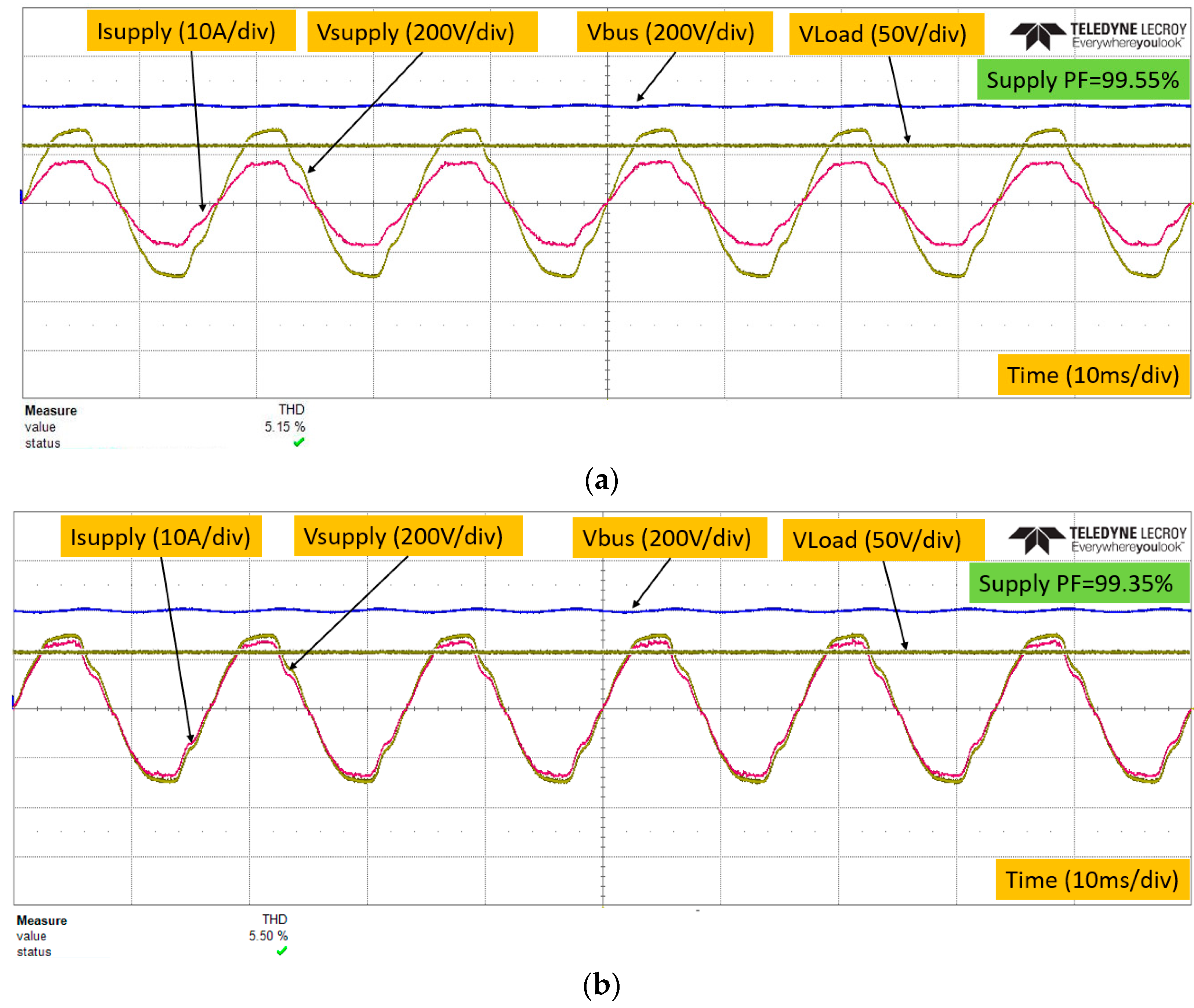
5. Experimental Verification and Discussions
6. Conclusions
Author Contributions
Funding
Conflicts of Interest
References
- Ortiz-Castrillón, J.R.; Mejía-Ruíz, G.E.; Muñoz-Galeano, N.; López-Lezama, J.M.; Saldarriaga-Zuluaga, S.D. PFC Single-Phase AC/DC Boost Converters: Bridge, Semi-Bridgeless, and Bridgeless Topologies. Appl. Sci. 2021, 11, 7651. [Google Scholar] [CrossRef]
- Gallo, C.A.; Tofoli, F.L.; Pinto, J.A. Two-stage isolated switch-mode power supply with high efficiency and high input power factor. IEEE Trans. Ind. Electron. 2010, 57, 3754–3766. [Google Scholar] [CrossRef]
- Yu, R.; Pong, B.M.; Ling, B.W.; Lam, J. Two-stage optimization method for efficient power converter design including light load operation. IEEE Trans. Power Electron. 2011, 27, 1327–1337. [Google Scholar]
- Baek, J.; Kim, J.K.; Lee, J.B.; Park, M.H.; Moon, G.W. A new standby structure integrated with boost PFC converter for server power supply. IEEE Trans. Power Electron. 2018, 34, 5283–5293. [Google Scholar] [CrossRef]
- Xiong, Y.; Huang, Y.; Zhong, Z.; Zhang, T. Research and design on digital PFC of 2kW On-board charger. World Electr. Veh. J. 2010, 4, 202–207. [Google Scholar] [CrossRef] [Green Version]
- Yang, F.; Li, C.; Cao, Y.; Yao, K. Two-phase interleaved boost PFC converter with coupled inductor under single-phase operation. IEEE Trans. Power Electron. 2019, 35, 169–184. [Google Scholar] [CrossRef]
- Tseng, S.Y.; Fan, J.H. Bridgeless Boost Converter with an Interleaving Manner for PFC Applications. Electronics 2021, 10, 296. [Google Scholar] [CrossRef]
- Okilly, A.H.; Baek, J. Optimal Design Analysis with Simulation and Experimental Performance Investigation of High-Power Density Telecom PFC Converters. Appl. Sci. 2021, 11, 7911. [Google Scholar] [CrossRef]
- Baek, J.; Park, M.H.; Kim, T.; Youn, H.S. Modified power factor correction (PFC) control and printed circuit board (PCB) design for high-efficiency and high-power density on-board charger. Energies 2021, 14, 605. [Google Scholar] [CrossRef]
- Kim, Y.S.; Sung, W.Y.; Lee, B.K. Comparative performance analysis of high density and efficiency PFC topologies. IEEE Trans. Power Electron. 2013, 29, 2666–2679. [Google Scholar] [CrossRef]
- Kim, D.J.; Park, J.H.; Lee, K.B. Scheme to improve the line current distortion of PFC using a predictive control algorithm. J. Power Electron. 2015, 15, 1168–1177. [Google Scholar] [CrossRef] [Green Version]
- Wang, J.; Eto, H.; Kurokawa, F. Optimal zero-voltage-switching method and variable on-time control for predictive boundary conduction mode boost PFC converter. IEEE Trans. Ind. Appl. 2019, 56, 527–540. [Google Scholar] [CrossRef]
- Kim, J.W.; Yi, J.H.; Cho, B.H. Enhanced variable on-time control of critical conduction mode boost power factor correction converters. J. Power Electron. 2014, 14, 890–898. [Google Scholar] [CrossRef] [Green Version]
- Karaarslan, A.H.; Iskender, I. A DSP based power factor correction converter to reduce total harmonic distortion of input current for improvement of power quality. Electr. Eng. 2011, 93, 247–257. [Google Scholar] [CrossRef]
- Khan, D.; Hu, P.; Habib, S.; Waseem, M.; Lin, Z.; Ahmed, E.M. A resonant damping control and analysis for LCL-type grid-connected inverter. Energy Rep. 2022, 8, 911–928. [Google Scholar] [CrossRef]
- Okilly, A.H.; Kim, N.; Baek, J. Inrush Current Control of High-Power Density DC–DC Converter. Energies 2020, 13, 4301. [Google Scholar] [CrossRef]
- Schmidt, J.M.; Sartori, H.C.; Pinheiro, J.R. Design methodology to achieve high-efficiency isolated ZVS DC/DC converters. In Proceedings of the IEEE 8th International Symposium on Power Electronics for Distributed Generation Systems (PEDG) 2017, Florianópolis, Brazil, 17–20 April 2017; pp. 1–8. [Google Scholar]
- Lee, Y.J.; Bak, Y.; Lee, K.B. Control method for phase-shift full-bridge center-tapped converters using a hybrid fuzzy sliding mode controller. Electronics 2019, 8, 705. [Google Scholar] [CrossRef] [Green Version]
- Das, P.; Laan, B.; Mousavi, S.A.; Moschopoulos, G. A nonisolated bidirectional ZVS-PWM active clamped DC–DC converter. IEEE Trans. Power Electron. 2009, 24, 553–558. [Google Scholar] [CrossRef]
- Escudero, M.; Kutschak, M.A.; Meneses, D.; Rodriguez, N.; Morales, D.P. A Practical Approach to the Design of a Highly Efficient PSFB DC-DC Converter for Server Applications. Energies 2019, 12, 3723. [Google Scholar] [CrossRef] [Green Version]
- Sayed, K.; Ali, Z.M.; Aldhaifallah, M. Phase-Shift PWM-Controlled DC–DC Converter with Secondary-Side Current Doubler Rectifier for On-Board Charger Application. Energies 2020, 13, 2298. [Google Scholar] [CrossRef]
- Ochoa, D.; Lázaro, A.; Zumel, P.; Sanz, M.; Rodriguez de Frutos, J.; Barrado, A. Small-Signal Modeling of Phase-Shifted Full-Bridge Converter Considering the Delay Associated to the Leakage Inductance. Energies 2021, 14, 7280. [Google Scholar] [CrossRef]
- Cho, I.H.; Cho, K.M.; Kim, J.W.; Moon, G.W. A new phase-shifted full-bridge converter with maximum duty operation for server power system. IEEE Trans. Power Electron. 2011, 26, 3491–3500. [Google Scholar] [CrossRef]
- Kathiresan, R.; Das, P.; Reindl, T.; Panda, S.K. A novel ZVS DC–DC full-bridge converter with hold-up time operation. IEEE Trans. Ind. Electron. 2017, 64, 4491–4500. [Google Scholar] [CrossRef]
- Hurley, W.G.; Wölfle, W.H. Transformers and Inductors for Power Electronics. Theory, Design and Applications; Wiley: London, UK, 2013. [Google Scholar]
- 015-Magnetics-Powder-Core-Catalog, Core Selector Charts. Available online: https://www.mag-inc.com/getattachment/Products/Powder-Cores/Learn-More-about-Powder-Cores/2015-Magnetics-Powder-Core-Catalog.pdf?lang=en-US (accessed on 19 April 2021).
- Magnetics Powder Cores Molypermalloy, High Flux, Kool Mµ, XFlux Selection Catalogues. Available online: https://www.mag-inc.com/getattachment/Products/Powder-Cores/Learn-More-about-Powder-Cores/2015-Magnetics-PowderCore-Catalog.pdf?lang=en-US (accessed on 24 January 2021).
- Understanding ESR in Electrolytic Capacitors. Available online: https://www.avnet.com (accessed on 15 April 2020).
- UCC28070 300-W Interleaved PFC Pre-Regulator Design Review. Application Report. Texas Instruments: Dallas, TX, USA, 2010. Available online: https://www.ti.com/lit/an/slua479b/slua479b.pdf?ts=1613536856416&ref_url=https%253A%252F%252Fwww.google.com%252F (accessed on 20 August 2021).
- Rasoulinezhad, R.; Abosnina, A.A.; Khodabakhsh, J.; Moschopoulos, G. An AC-DC Interleaved ZCS-PWM Boost Converter with Reduced Auxiliary Switch RMS Current Stress. IEEE Access 2021, 9, 41320–41333. [Google Scholar] [CrossRef]
- Li, R.T.H.; Chung, H.S.H.; Sung, A.K.T. Passive Lossless Snubber for Boost PFC with Minimum Voltage and Current Stress. IEEE Trans. Power Electron. 2010, 25, 602–613. [Google Scholar] [CrossRef]
- Mejía-Ruiz, G.E.; Muñoz-Galeano, N.; López-Lezama, J.M. Modeling and development of a bridgeless PFC Boost rectifier. Rev. Fac. Ing. Univ. Antioq. 2017, 82, 9–21. [Google Scholar] [CrossRef] [Green Version]
- Bahmani, M. Design and Optimization of hf Transformers for High Power dc-dc Applications; Chalmers university: Göteborg, Sweden, 2014. [Google Scholar]
- Ruiz, D.; Ortíz, J.; Moreno, E.; Fuerte, C.; Venegas, V.; Vargas, A.; Vergara, H. Ferrites and Nanocrystalline Alloys Applied to DC–DC Converters for Renewable Energies. Appl. Sci. 2022, 12, 709. [Google Scholar] [CrossRef]
- Zhao, Z.; Xu, Q.; Dai, Y.; Yin, H. Analysis, Design, and Implementation of Improved LLC Resonant Transformer for Efficiency Enhancement. Energies 2018, 11, 3288. [Google Scholar] [CrossRef] [Green Version]
- “Ferrite for Switching Power Supplies” TDK Products Catalogue. Available online: https://www.jp.tdk.com/tefe02/e140_1.pdf (accessed on 15 January 2022).
- Yue, S.; Yang, Q.; Li, Y.; Zhang, C.; Xu, G. Core loss calculation of the soft ferrite cores in high frequency transformer under non-sinusoidal excitations. In Proceedings of the 20th International Conference on Electrical Machines and Systems (ICEMS), Sydney, NSW, Australia, 11–14 August 2017; pp. 1–5. [Google Scholar]
- Phase-Shifted Full-Bridge, Zero-Voltage Transition Design Considerations. Application Report. Available online: https://www.ti.com/lit/pdf/slua107 (accessed on 8 March 2020).
- Tao, H.; Zhang, G.; Zheng, Z.; Du, C. Design of Digital Control System for DC/DC Converter of On-Board Charger. J. Adv. Transp. 2019, 2019, 2467307. [Google Scholar] [CrossRef] [Green Version]
- Modeling, Analysis and Compensation of the Current-Mode Converter; Notes, Application; Texas Instruments Inc.: Dallas, TX, USA, 1999.
- “500 W Fully Digital AC-DC Power Supply (D-SMPS) Evaluation Board” Application Note, STMicroelectronics Company. Available online: http://www.st.com/ (accessed on 9 June 2022).
- “94.5% Efficiency, 500W industrial AC-DC Reference Design” Application Note, Texas Instruments. Available online: https://www.ti.com/tool/TIDA-010015 (accessed on 9 June 2022).
- “800 W Platinum® Server Power Supply” Application Note, Infineon Company. Available online: http://www.infineon.com/ (accessed on 9 June 2022).
- “1-kW, 80 Plus Titanium, GaN CCM Totem Pole Bridgeless PFC and Half-Bridge LLC Reference Design” Application Note, Texas Instruments. Available online: https://www.ti.com/tool/TIDA-010062 (accessed on 10 June 2022).
- “EVAL_1K6W_PSU_G7_DD—Infineon Technologies” Application Note, Infineon Company. Available online: https://www.infineon.com/eval-1k6w-psu-G7-DD (accessed on 10 June 2022).


| Design Parameter | Value | Unit |
|---|---|---|
| Operating voltage (Vs) | 220 (176–264) | V |
| Operating Frequency (Fs) | 60 (57–63) | Hz |
| DC bus Voltage (Vbus) | 400 (320–410) | V |
| Rated Power (Po) | 2000 | W |
| Target Efficiency (η) | 97% | - |
| Target power factor (PF) | 99% | - |
| PFC Switching Frequency (Fsw) | 100 | kHz |
| Hold Up Time (thu) | 6 | ms |
| Inductor ripple current (%Ripple) | 15% | - |
| DC bus voltage ripple (Vrpp) | 15 | Vpp |
| Parameter | Value |
|---|---|
| Actual inductance Peak current Core type | 470 uF 11.60 A 2 stacked Kool Mµ (77083A7) |
| Inductive factor (AL) | 81 ± 8% (nH/T2) |
| No. of Turns (NLb) | 60 |
| Winding wire | Copper 1.15 mm |
| DC resistance (DCR) | 0.087 Ω |
| Component | Quant. | Part Number/Description | Power Loss (W) | Efficiency |
|---|---|---|---|---|
| Bridge rectifier | 2 | GSIB 2580 | 21.32 | 97.10% |
| Boost inductor Lb | 1 | Core: (2 stacked cores Kool Mμ (77083A7). Single 1.15 Copper wire 60 Turns | 17.12 | |
| Mosfet Qb | 1 | IPZ60R040C7 | 6.85 | |
| Diode Db | 1 | IDH16G65C5 | 9.375 | |
| DC bus capacitor Cb | 2 | EKMR421VSN561MR50S | 3.90 |
| Parameter | Value | Unit |
|---|---|---|
| Input voltage (Vbus) | 400 (320–410) | V |
| Load voltage (Vload) | 54 (45–63) | V |
| Output voltage ripple | 200 | mV |
| Rated power (Pload) | 2000 | W |
| Switching frequency | 100 | kHz |
| Target efficiency | 95% | |
| holdup time (thold) Inductor ripple current | 20 15% | us |
| Parameter | Resonant Inductor | Load Filter Inductor |
|---|---|---|
| Actual inductance Peak current Core type | 31 uF 7.96 A Single Kool Mu (77120A7) | 30 uF 39.80 A Single Kool Mu (77439A9) |
| Inductive factor | 72 ± 8% (nH/T2) | 135 ± 8% (nH/T2) |
| No. of Turns | 22 | 16 |
| Winding wire | Single copper wire 1.15 mm | 3-Wire copper 1.15 mm |
| DC resistance (DCR) | 0.013 Ω | 0.0029 Ω |
| Component | Quantity | Part Number/Description | Power Loss (W) | Efficiency |
|---|---|---|---|---|
| Input capacitance | 1 | EETHC2W471LC | 2.40 | 97.00% |
| Primary Mosfets | 4 | IPW60R070CFD7 | 12.92 | |
| Resonant inductor | 1 | Core: Kool Mu 77120A7 Single wire of 1.15 mm copper 22 Turns | 1.815 | |
| H.F transformer | 1 | Core: PQ40/40 Turns ratio: 20:4:4 Lm = 2.8 mH | 7.13 | |
| Secondary Mosfets | 4 | IPP110N20N3 | 19.26 | |
| Filter inductor | 1 | Core: Kool Mu 77439A9 3-wire of 1.15 mm copper 16 Turns | 15.50 | |
| Filter capacitor | 7 | SamYoung 470 uF 63V | 0.825 |
| Component | Power Loss (W) |
|---|---|
| Bridge rectifier | 20.10 |
| Boost inductor Lb | 17.25 |
| Mosfet Qb | 6.10 |
| Diode Db | 9.00 |
| DC bus capacitor Cb | 3.90 |
| Input capacitance | 2.40 |
| Primary Mosfets | 11.45 |
| Resonant inductor | 1.65 |
| H.F transformer | 6.45 |
| Secondary Mosfets | 17.65 |
| Filter inductor | 14.35 |
| Filter capacitor | 0.825 |
| Design Reference | Design Topology | Power (W) | Efficiency (%) | PF (%) | THD (%) |
|---|---|---|---|---|---|
| proposed | Two stage AC-DC Conventional PFC PS-ZVS converter | 2000 | 93.15 | 99.35 | 5.50 |
| [41] | Two stage AC-DC Bridgeless PFC LLC converter | 500 | 93.20 | 98.90 | 7.40 |
| [42] | Two stage AC-DC interleaved PFC LLC converter | 500 | 94.55 | 99.00 | 8 |
| [43] | Two stage AC-DC Conventional PFC LLC converter | 800 | 94.47 | 99.50 | 2 |
| [44] | Two stage AC-DC Totem pole bridgeless PFC Half bridge LLC converter | 1000 | 96.99 | 96.20 | 8.96 |
| [45] | Two stage AC-DC bridgeless PFC LLC converter | 1600 | 94.20 | 98.90 | 4 |
Publisher’s Note: MDPI stays neutral with regard to jurisdictional claims in published maps and institutional affiliations. |
© 2022 by the authors. Licensee MDPI, Basel, Switzerland. This article is an open access article distributed under the terms and conditions of the Creative Commons Attribution (CC BY) license (https://creativecommons.org/licenses/by/4.0/).
Share and Cite
Okilly, A.H.; Baek, J. Design and Fabrication of an Isolated Two-Stage AC–DC Power Supply with a 99.50% PF and ZVS for High-Power Density Industrial Applications. Electronics 2022, 11, 1898. https://doi.org/10.3390/electronics11121898
Okilly AH, Baek J. Design and Fabrication of an Isolated Two-Stage AC–DC Power Supply with a 99.50% PF and ZVS for High-Power Density Industrial Applications. Electronics. 2022; 11(12):1898. https://doi.org/10.3390/electronics11121898
Chicago/Turabian StyleOkilly, Ahmed H., and Jeihoon Baek. 2022. "Design and Fabrication of an Isolated Two-Stage AC–DC Power Supply with a 99.50% PF and ZVS for High-Power Density Industrial Applications" Electronics 11, no. 12: 1898. https://doi.org/10.3390/electronics11121898