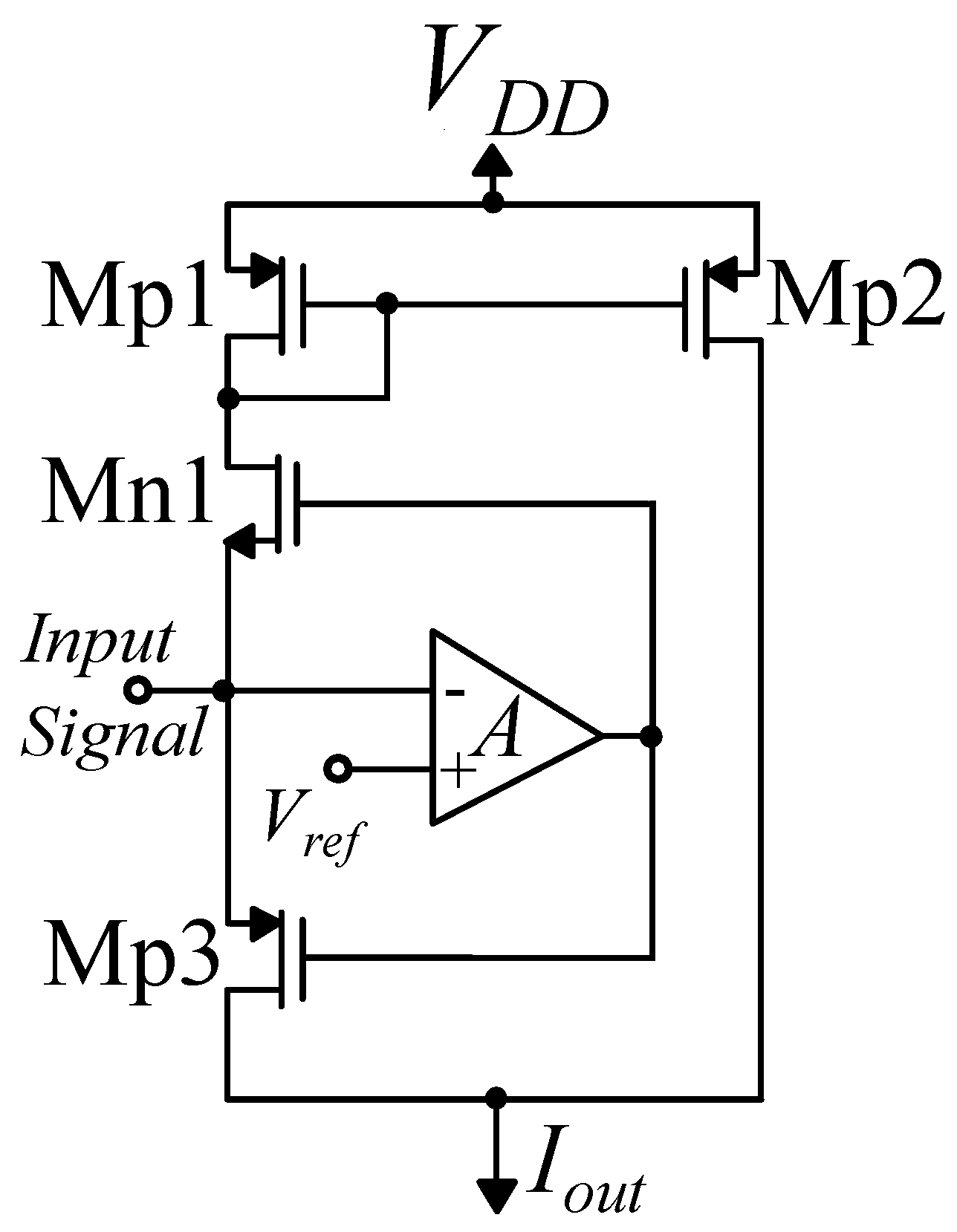
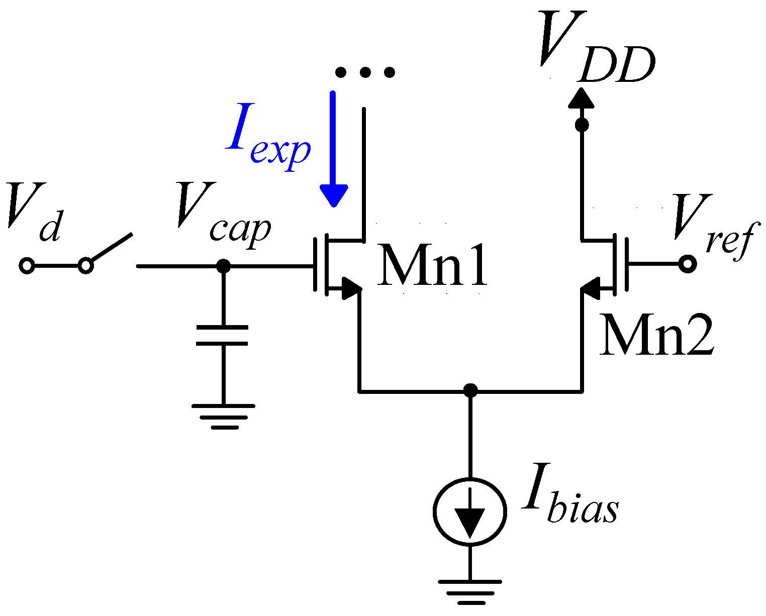
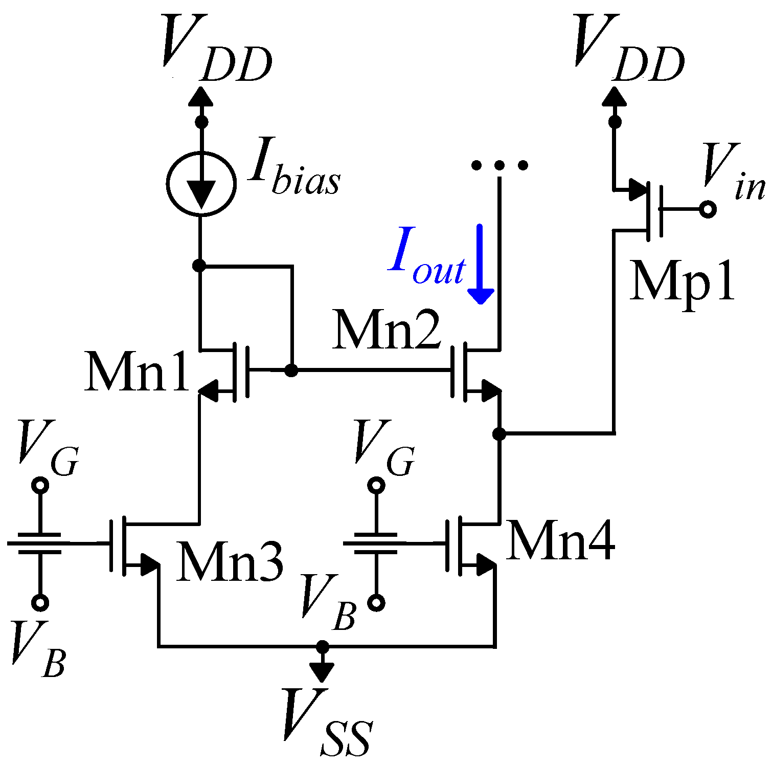
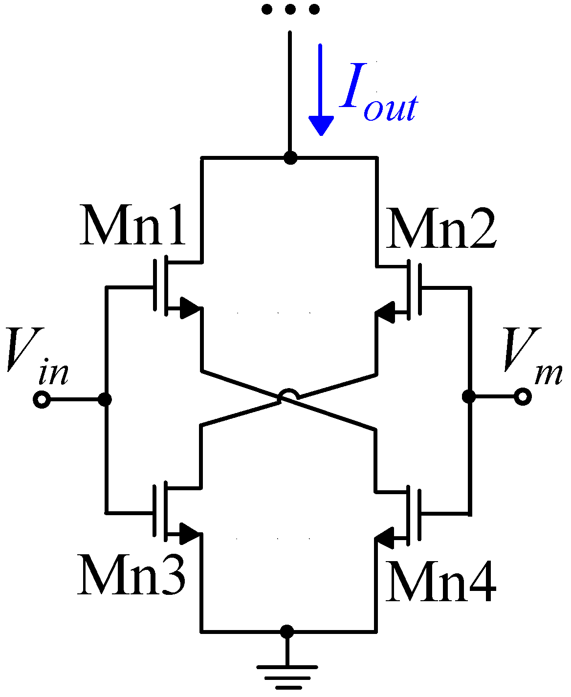
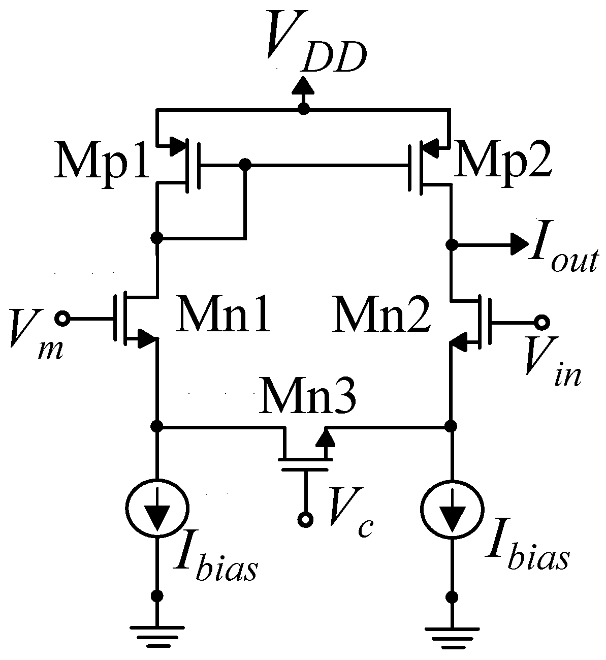
Figure 1.
Delbruck’s Simple Bump transistor level implementation.
Figure 1.
Delbruck’s Simple Bump transistor level implementation.
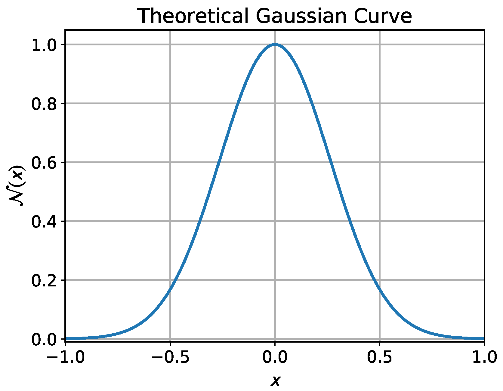
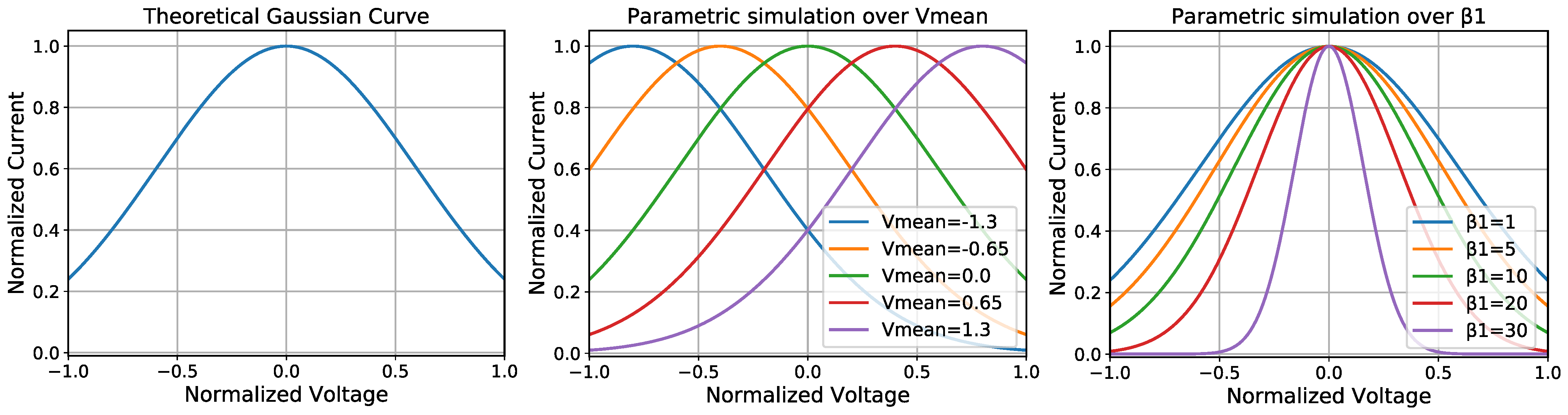
Figure 2.
Theoretical Gaussian Function Curve.
Figure 2.
Theoretical Gaussian Function Curve.
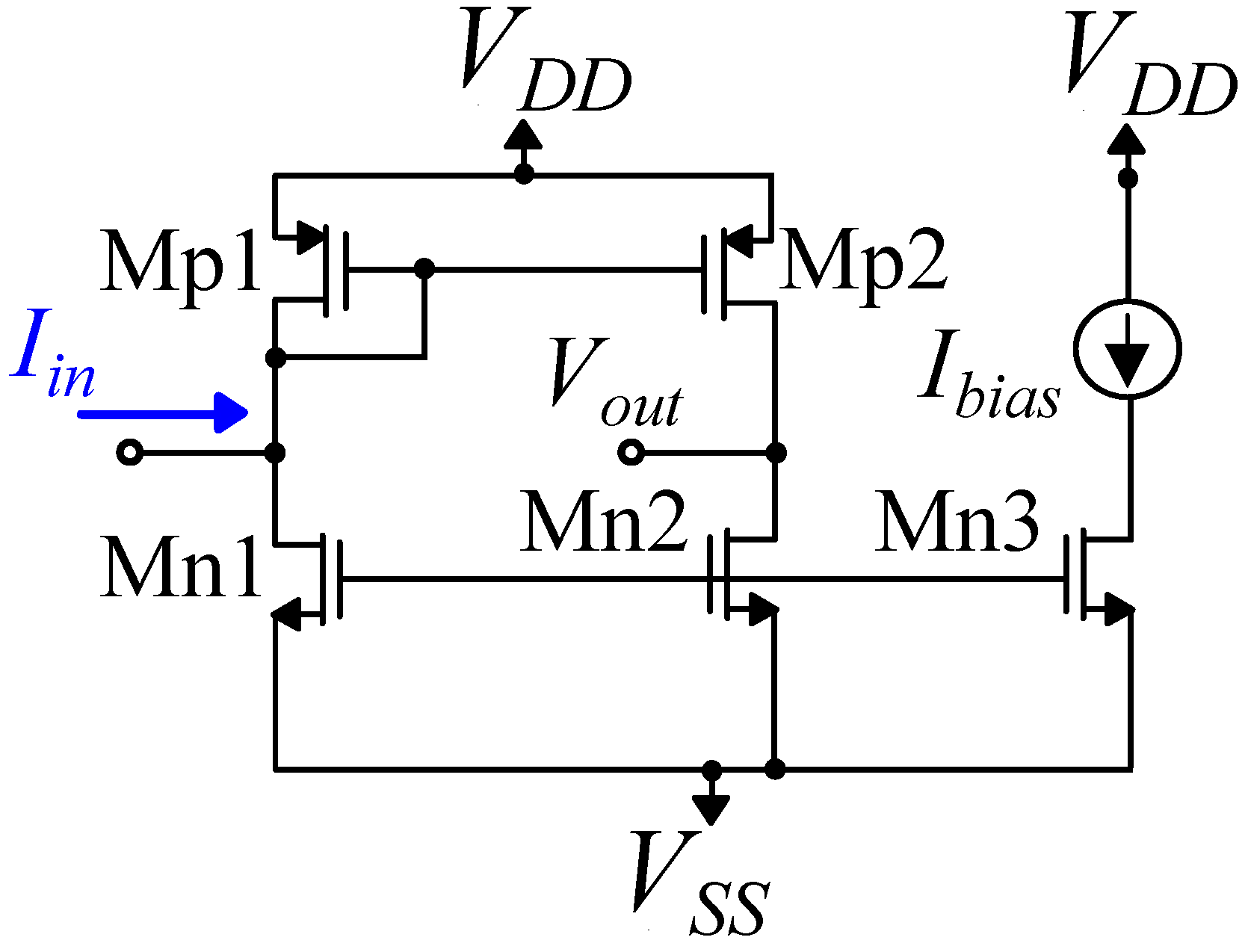
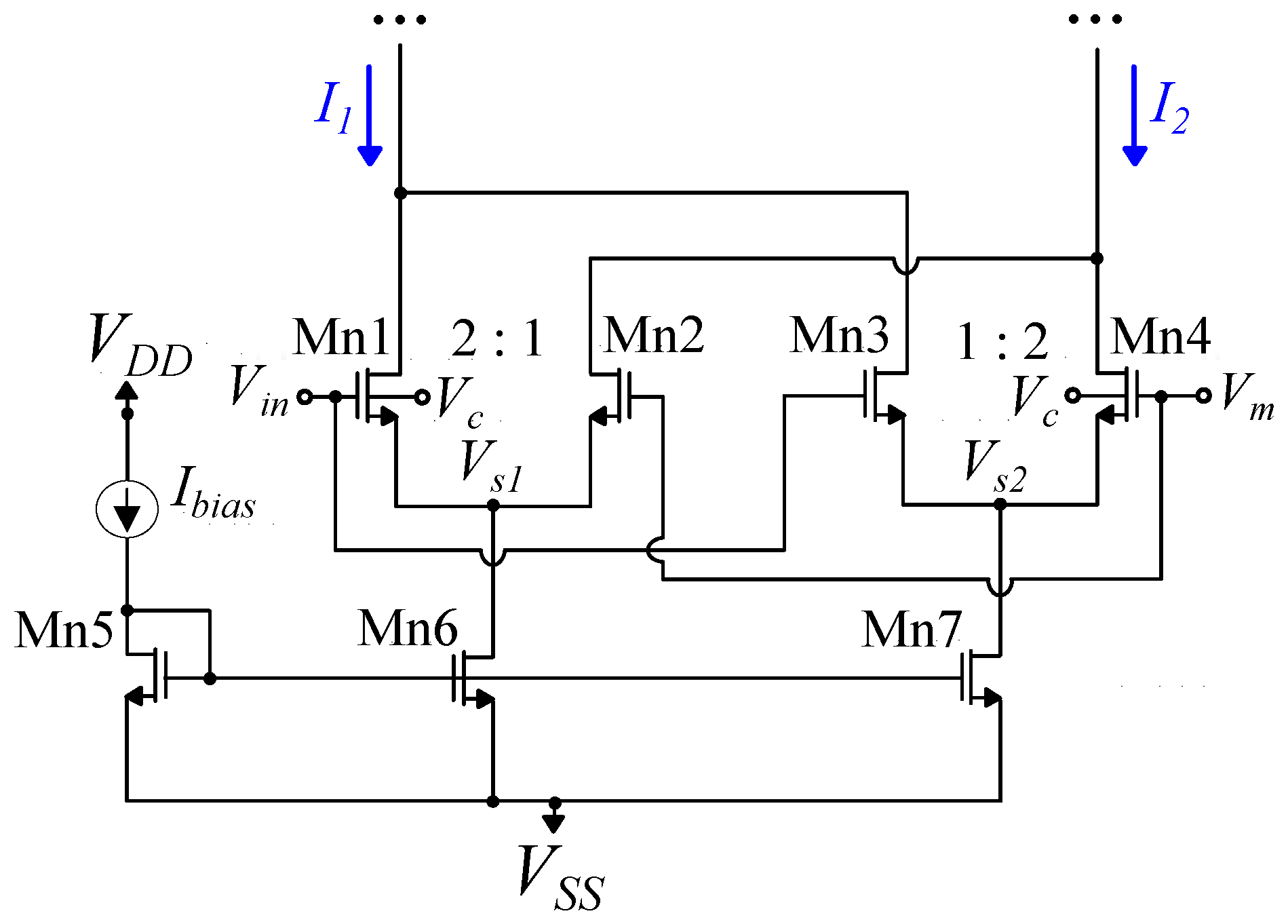
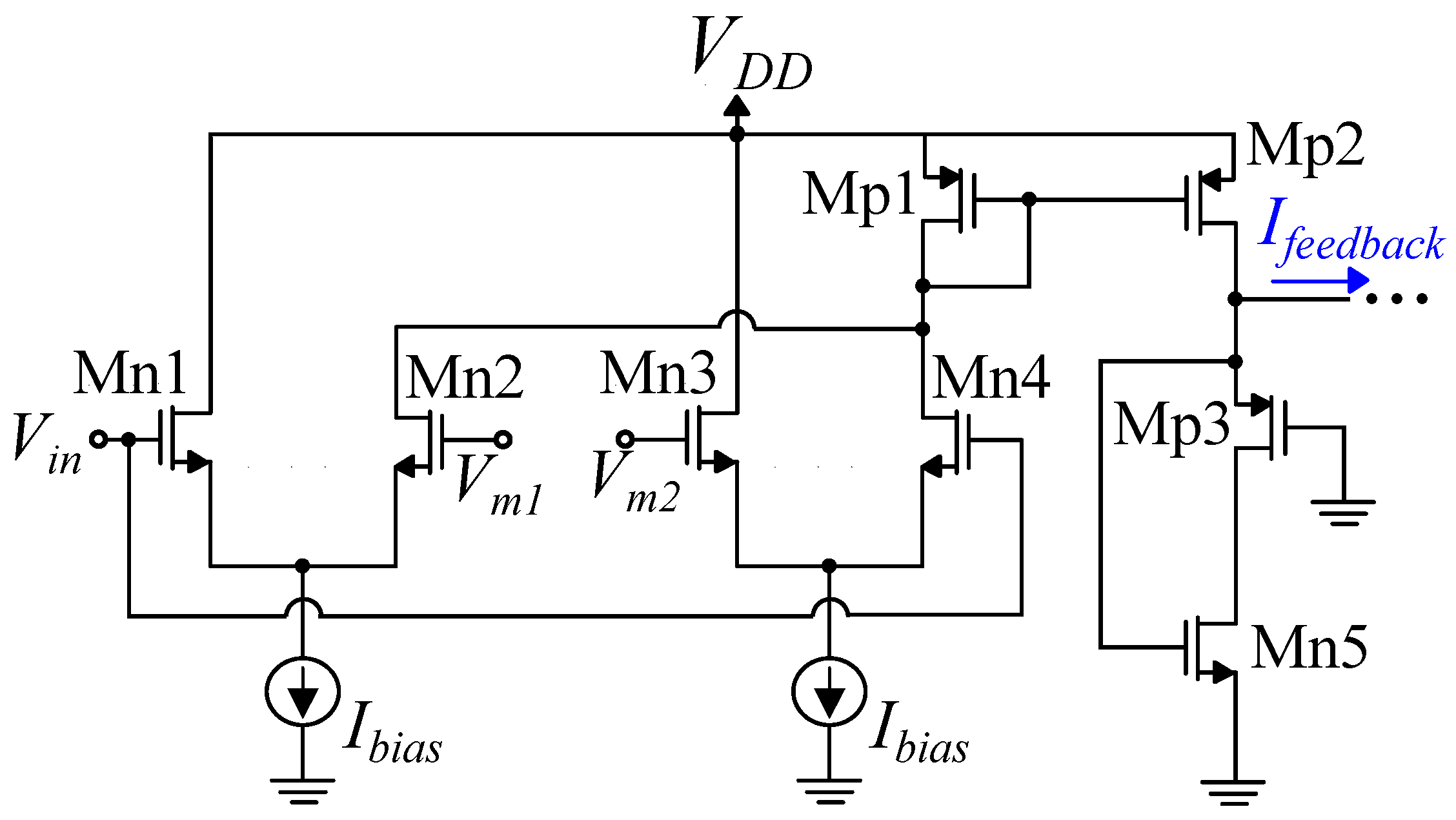
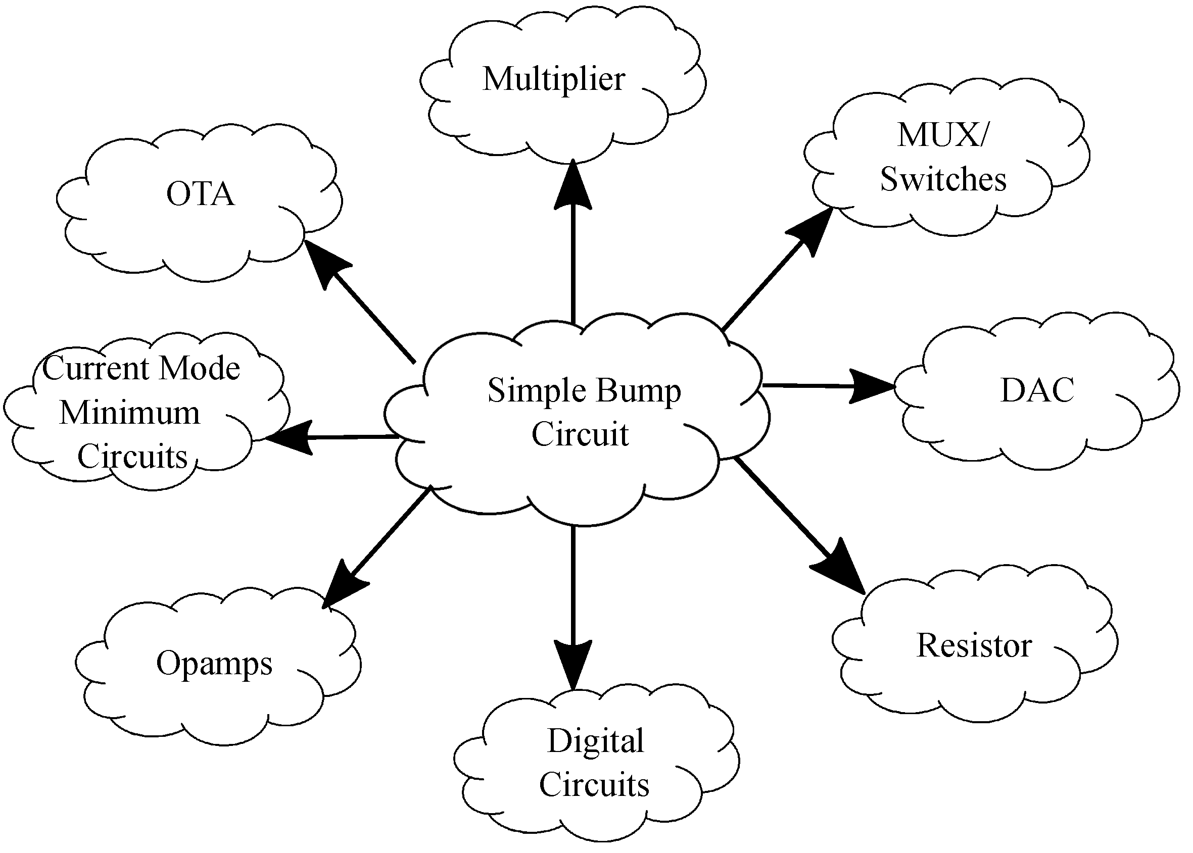
Figure 3.
Block diagram of a generic Gaussian function circuit (inspired by Delbruck’s Simple Bump).
Figure 3.
Block diagram of a generic Gaussian function circuit (inspired by Delbruck’s Simple Bump).
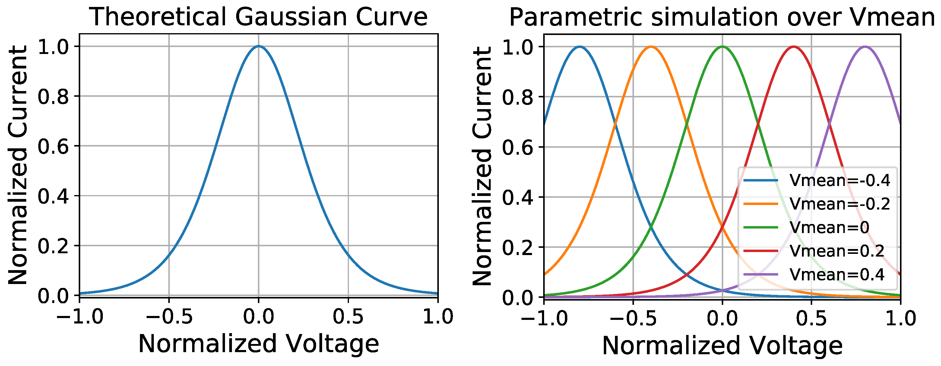
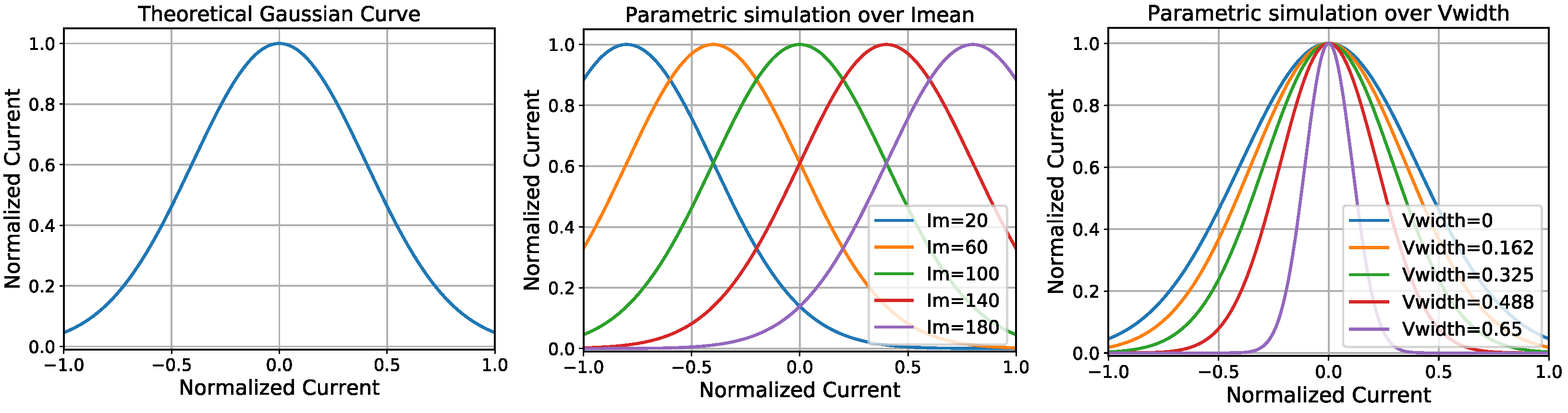
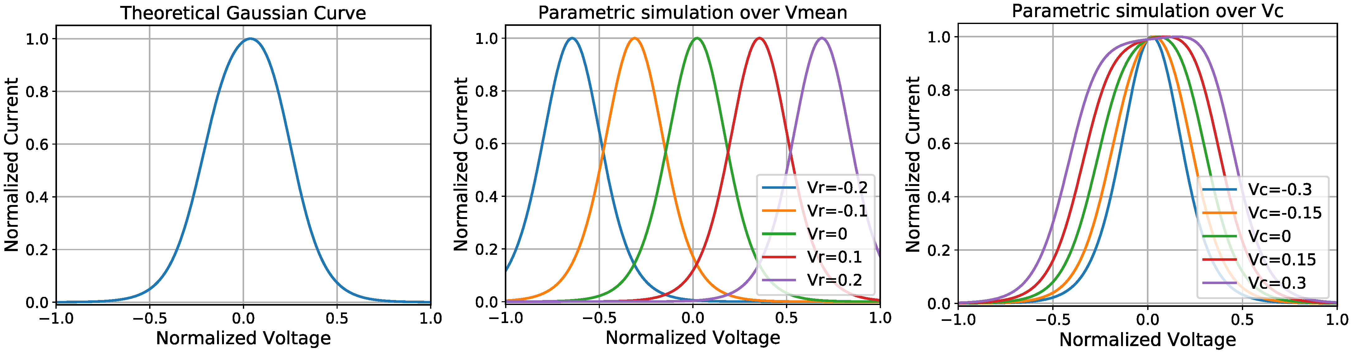
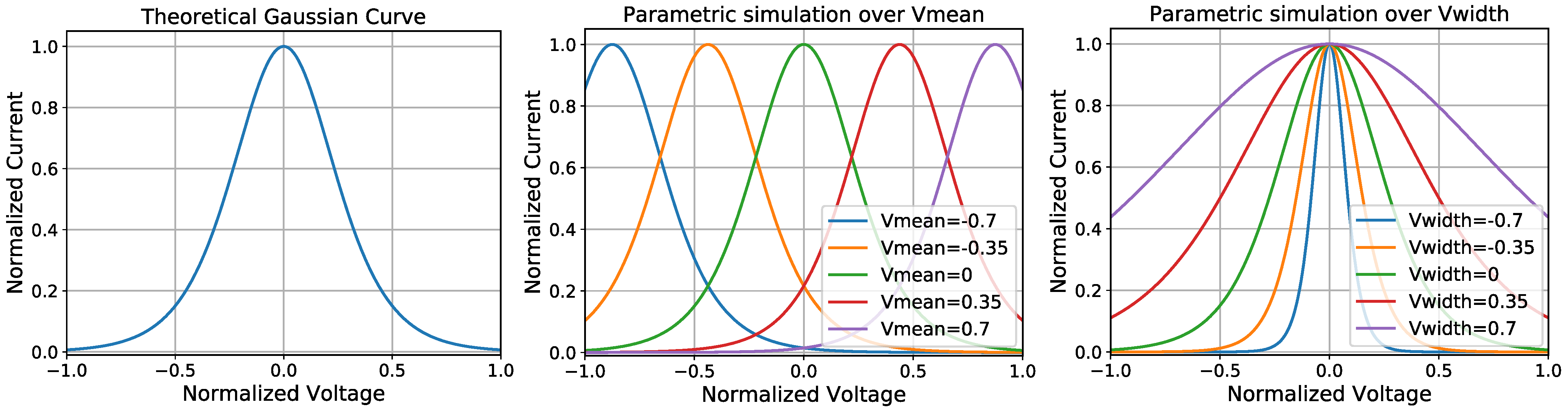
Figure 4.
Theoretical output current of Delbruck’s Simple Bump (left) Simulation for (right) Parametric simulation over .
Figure 4.
Theoretical output current of Delbruck’s Simple Bump (left) Simulation for (right) Parametric simulation over .
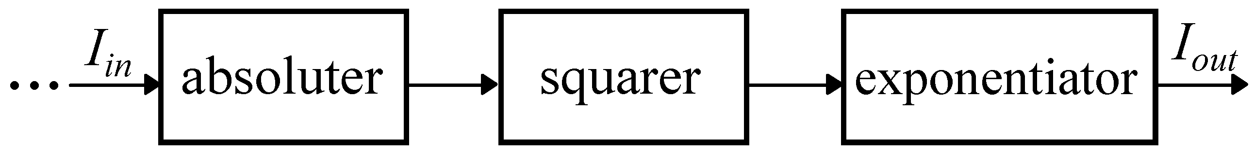
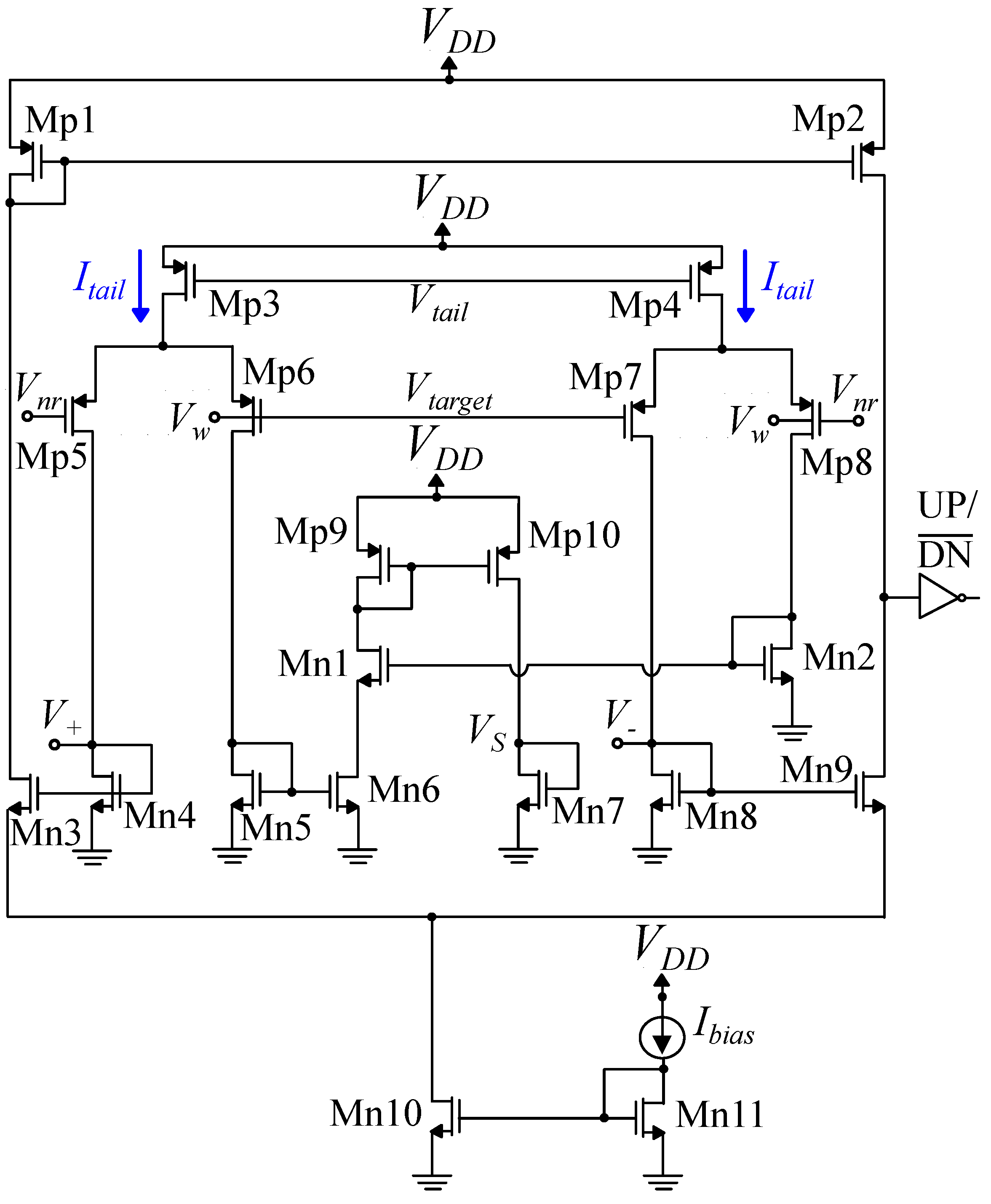
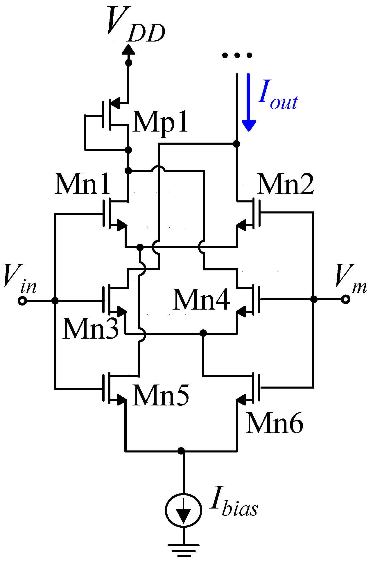
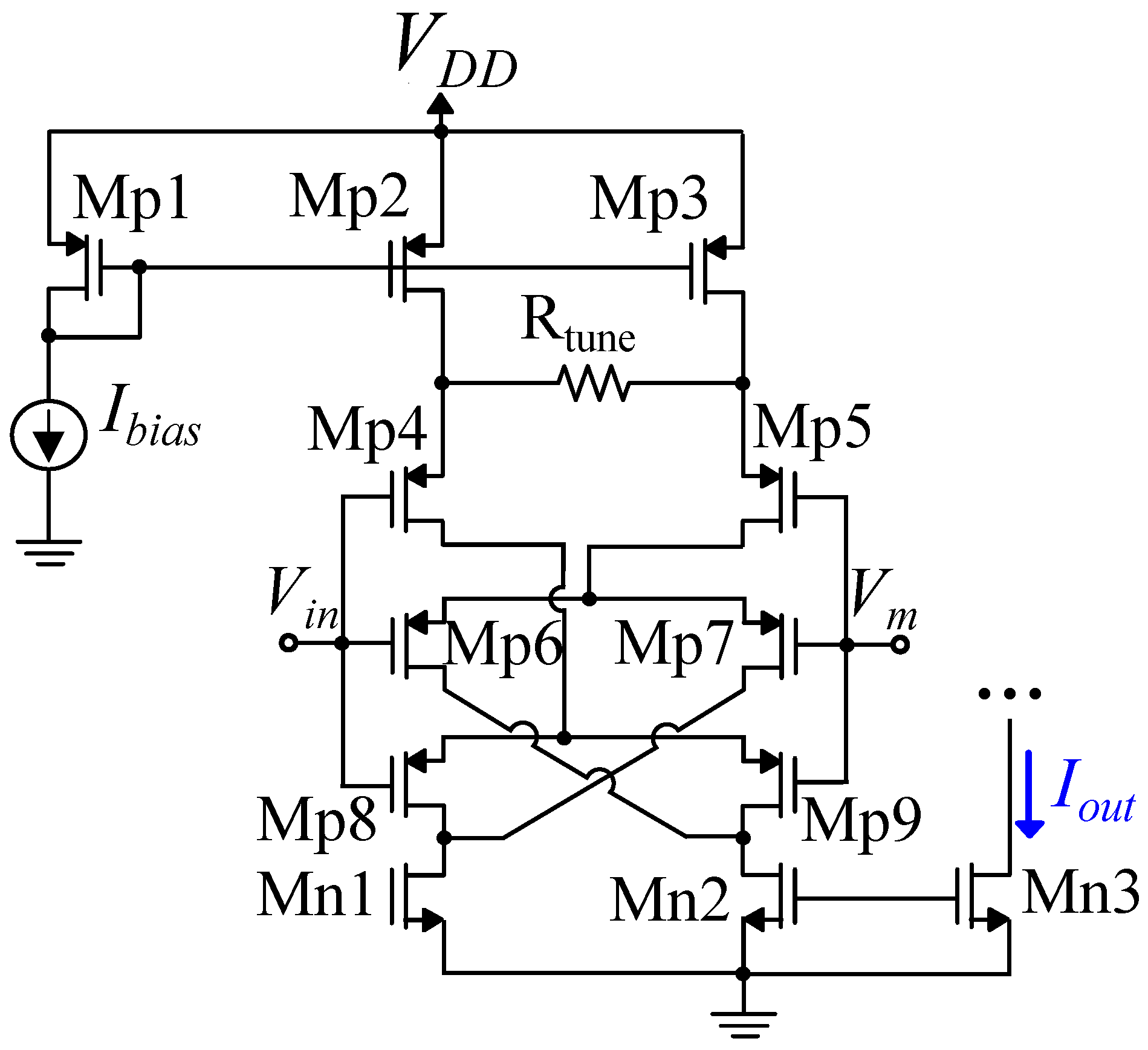
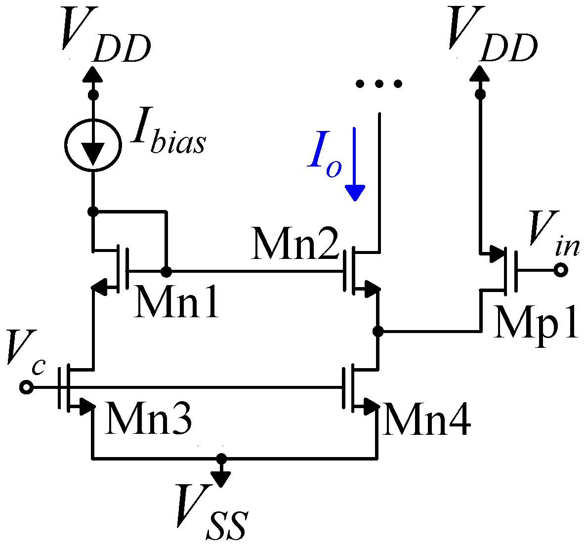
Figure 5.
Design flow diagram for the implementation of the Gaussian function based on the translinear principle.
Figure 5.
Design flow diagram for the implementation of the Gaussian function based on the translinear principle.
Figure 6.
An example schematic of an absolute value circuit.
Figure 6.
An example schematic of an absolute value circuit.
Figure 7.
A different approach to an absolute value circuit’s transistor level implementation.
Figure 7.
A different approach to an absolute value circuit’s transistor level implementation.
Figure 8.
An example transistor level implementation of a squarer divider circuit.
Figure 8.
An example transistor level implementation of a squarer divider circuit.
Figure 9.
An example transistor level implementation of a basic squarer block.
Figure 9.
An example transistor level implementation of a basic squarer block.
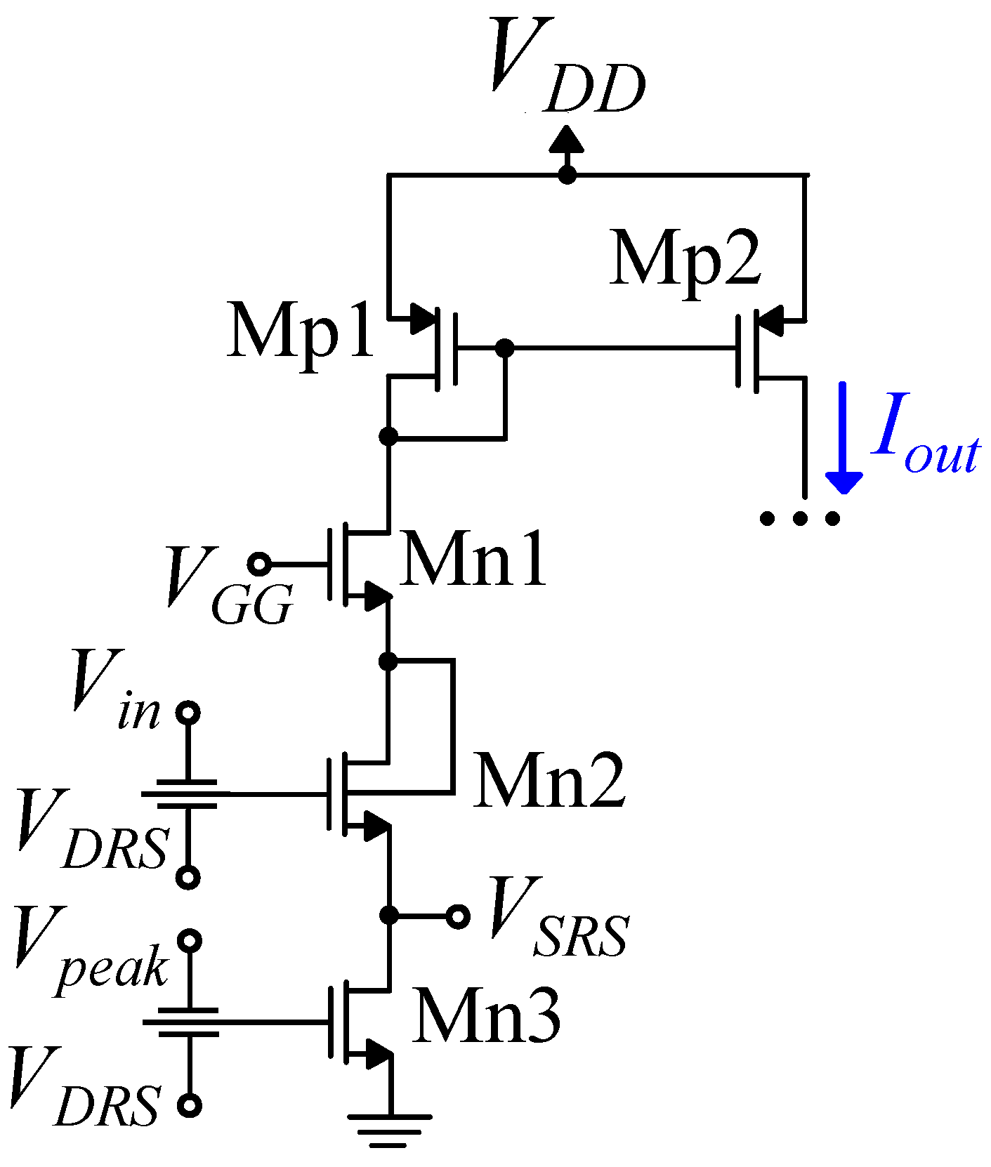
Figure 10.
A schematic of a simple exponential generation circuit.
Figure 10.
A schematic of a simple exponential generation circuit.
Figure 11.
Transistor level implementation of a current to voltage (I-V) converter.
Figure 11.
Transistor level implementation of a current to voltage (I-V) converter.
Figure 12.
Theoretical output current of an example of a circuit based on the Translinear Principle (left) Simulation for and (center) Parametric simulation over for (right) Parametric simulation over for .
Figure 12.
Theoretical output current of an example of a circuit based on the Translinear Principle (left) Simulation for and (center) Parametric simulation over for (right) Parametric simulation over for .
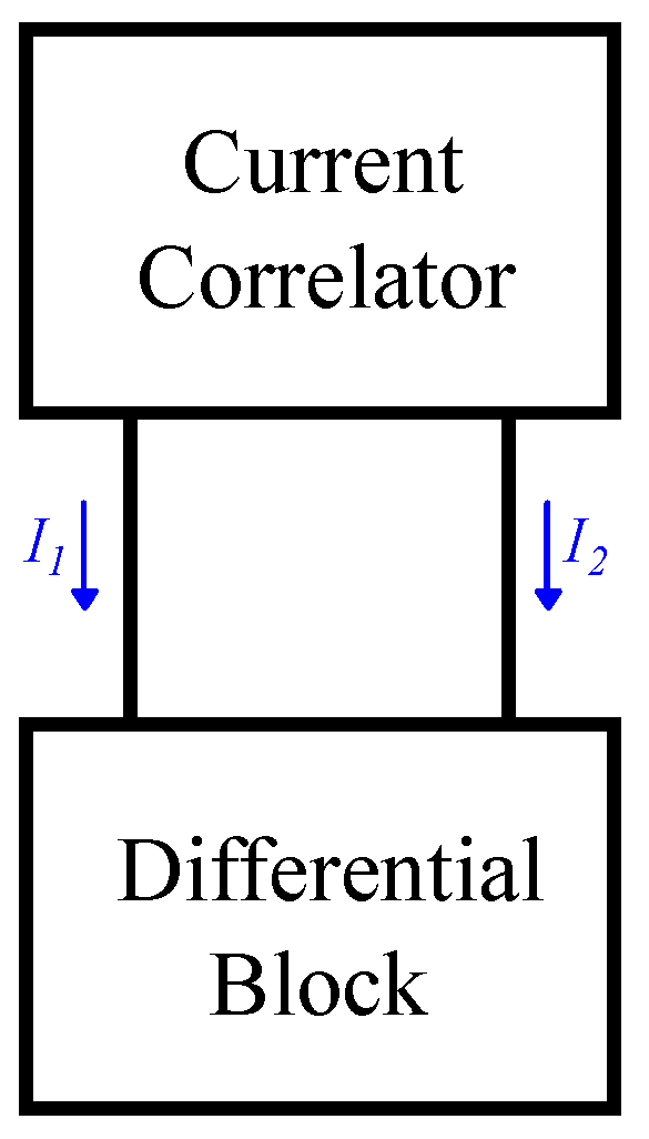
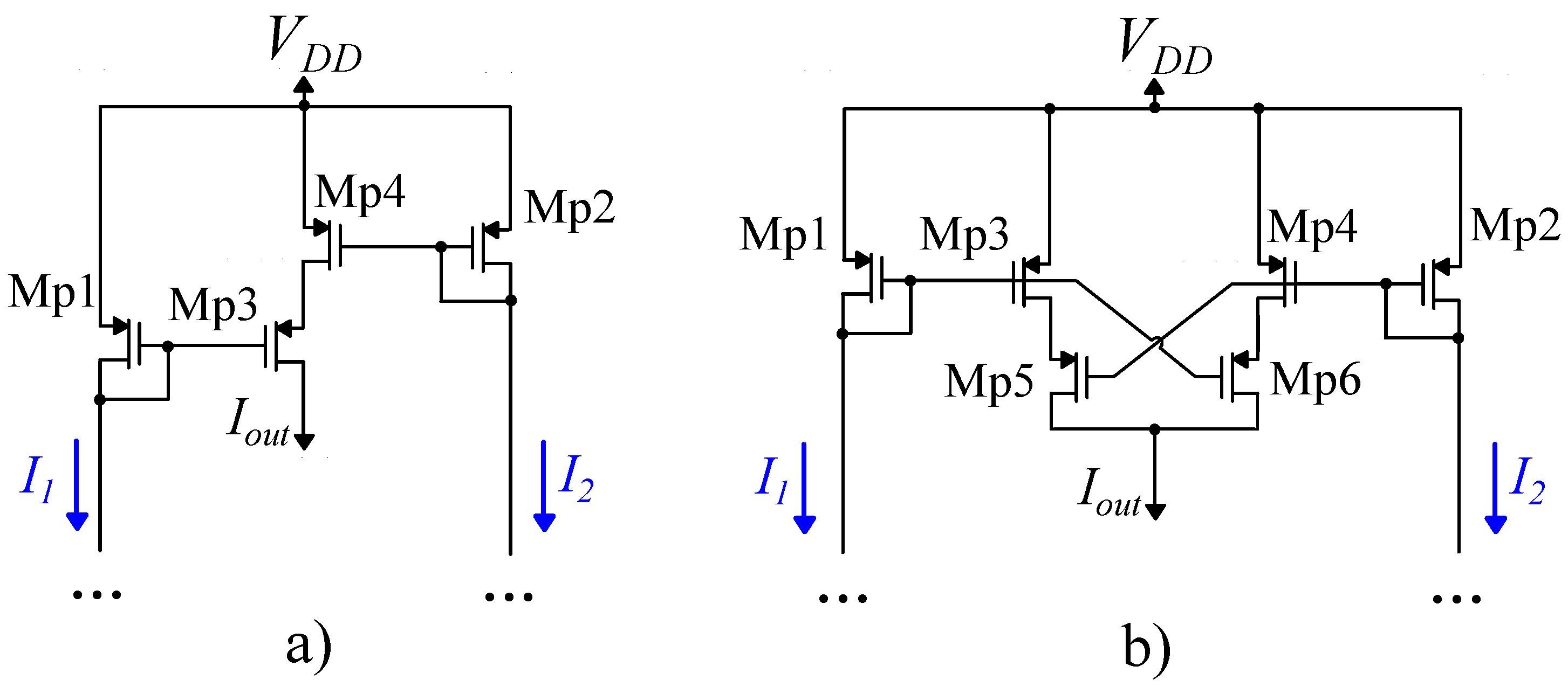
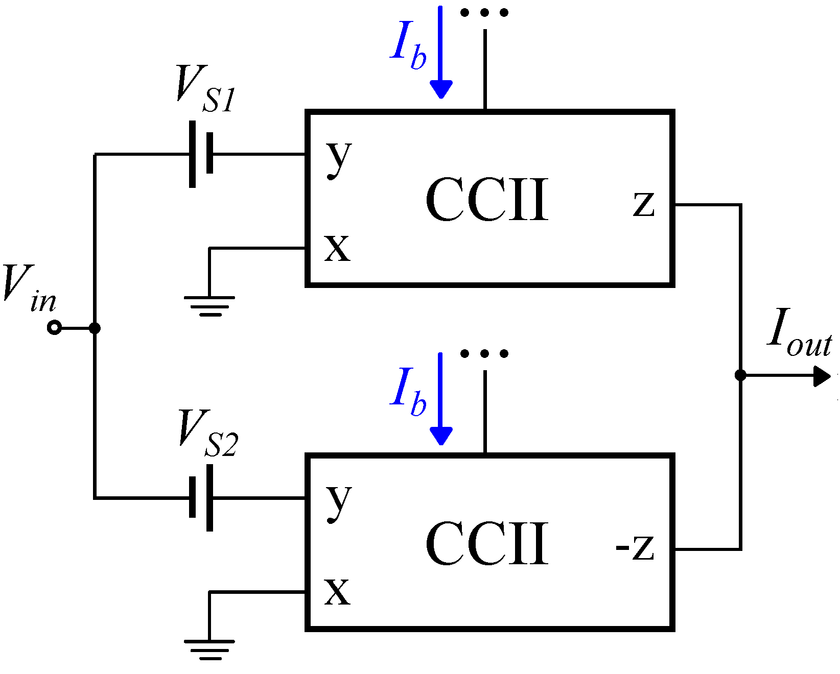
Figure 13.
Transistor level implementation of (a) a non symmetric current correlator and (b) a symmetric current correlator.
Figure 13.
Transistor level implementation of (a) a non symmetric current correlator and (b) a symmetric current correlator.
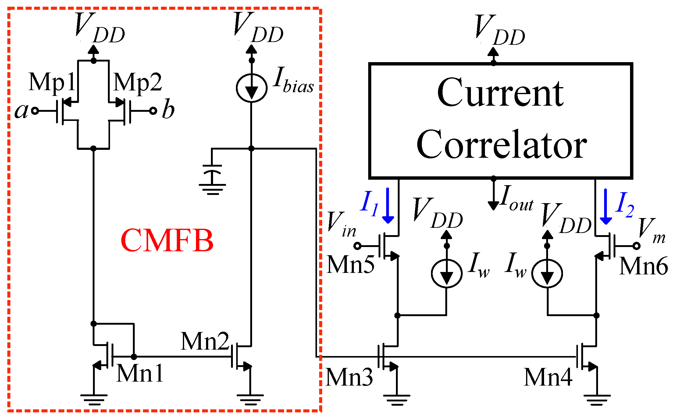
Figure 14.
Transistor level implementation of a differential difference block.
Figure 14.
Transistor level implementation of a differential difference block.
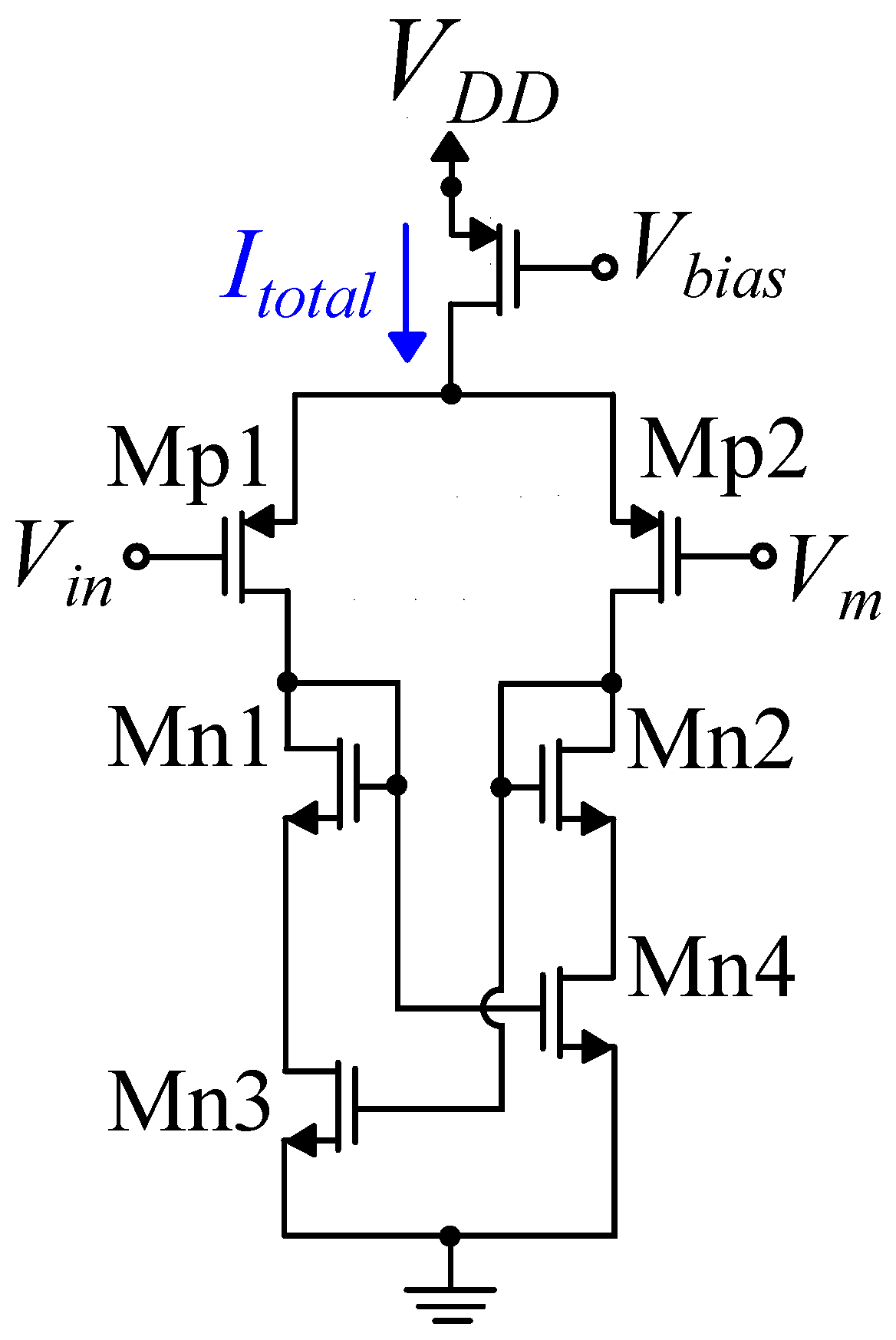
Figure 15.
Transistor level implementation of a versatile differential block.
Figure 15.
Transistor level implementation of a versatile differential block.
Figure 16.
An example of a fully tunable, bulk-controlled Gaussian function circuit.
Figure 16.
An example of a fully tunable, bulk-controlled Gaussian function circuit.
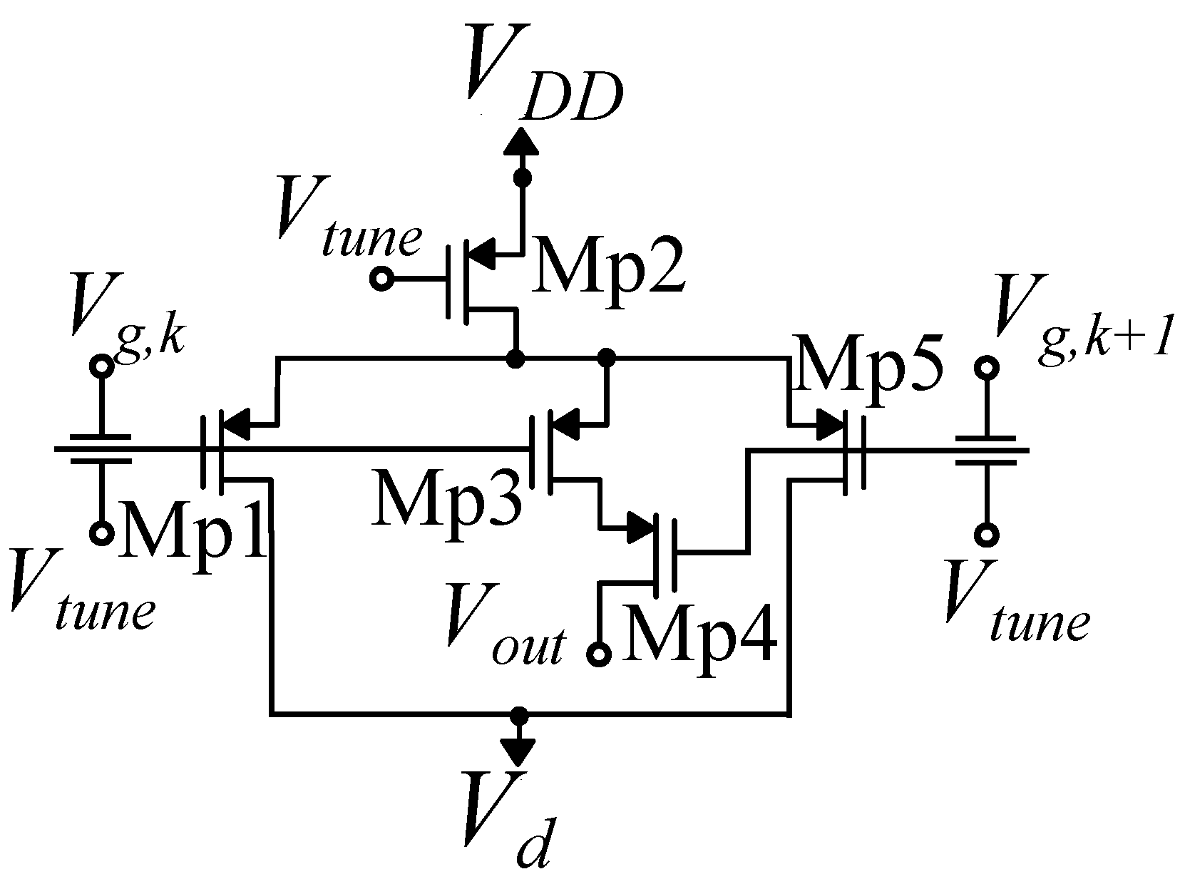
Figure 17.
Transistor level implementation of the VWbump, which has electrical control over the Gaussian function curve’s variance.
Figure 17.
Transistor level implementation of the VWbump, which has electrical control over the Gaussian function curve’s variance.
Figure 18.
Theoretical output function of an example of a bulk-controlled circuit (left) Simulation for and (center) Parametric simulation over for (right) Parametric simulation over for .
Figure 18.
Theoretical output function of an example of a bulk-controlled circuit (left) Simulation for and (center) Parametric simulation over for (right) Parametric simulation over for .
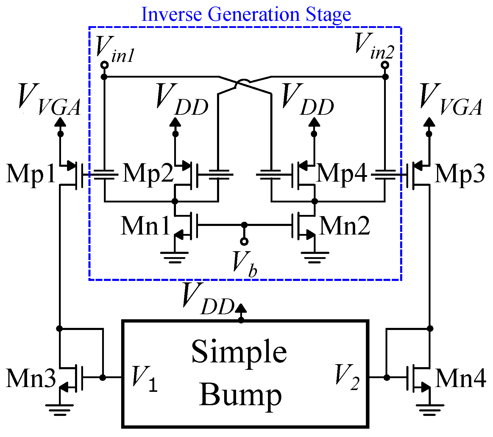
Figure 19.
Schematic of a Gaussian function circuit with a floating gate transistor based inverse generation block.
Figure 19.
Schematic of a Gaussian function circuit with a floating gate transistor based inverse generation block.
Figure 20.
A floating gate transistor based modification of a bump–antibump circuit.
Figure 20.
A floating gate transistor based modification of a bump–antibump circuit.
Figure 21.
A modification of an exponential-based Gaussian function circuit, using floating gate transistors.
Figure 21.
A modification of an exponential-based Gaussian function circuit, using floating gate transistors.
Figure 22.
Floating gate transistor level architecture based on an exponentiator circuit for the implementation of the Gaussian function.
Figure 22.
Floating gate transistor level architecture based on an exponentiator circuit for the implementation of the Gaussian function.
Figure 23.
Theoretical output function of an example of a floating gate based circuit (left) Simulation for and (center) Parametric simulation over for (right) Parametric simulation over for .
Figure 23.
Theoretical output function of an example of a floating gate based circuit (left) Simulation for and (center) Parametric simulation over for (right) Parametric simulation over for .
Figure 24.
An example of a Gaussian function circuit using only differential pairs.
Figure 24.
An example of a Gaussian function circuit using only differential pairs.
Figure 25.
Gilbert’s Gaussian circuit.
Figure 25.
Gilbert’s Gaussian circuit.
Figure 26.
An area-efficient version of Gilbert’s Gaussian circuit.
Figure 26.
An area-efficient version of Gilbert’s Gaussian circuit.
Figure 27.
Theoretical output function of an example of a circuit built with differential pairs (left) Simulation for and (center) Parametric simulation over for (right) Parametric simulation over for .
Figure 27.
Theoretical output function of an example of a circuit built with differential pairs (left) Simulation for and (center) Parametric simulation over for (right) Parametric simulation over for .
Figure 28.
A general flow chart, presenting potential extra components of fully tunable Gaussian function circuit architectures.
Figure 28.
A general flow chart, presenting potential extra components of fully tunable Gaussian function circuit architectures.
Figure 29.
A Gaussian function circuit with a CMFB stage.
Figure 29.
A Gaussian function circuit with a CMFB stage.
Figure 30.
A modified Gilbert’s Gaussian circuit, using a series of resistors controlled via switches.
Figure 30.
A modified Gilbert’s Gaussian circuit, using a series of resistors controlled via switches.
Figure 31.
A Gaussian function circuit using a multiplexer to adjust the multiplicity of the transistors in the differential pairs. (a) schematic (b) block for selecting transistors with different dimensions via the multiplexer.
Figure 31.
A Gaussian function circuit using a multiplexer to adjust the multiplicity of the transistors in the differential pairs. (a) schematic (b) block for selecting transistors with different dimensions via the multiplexer.
Figure 32.
A current conveyor second generation based Gaussian function circuit.
Figure 32.
A current conveyor second generation based Gaussian function circuit.
Figure 33.
Gaussian function circuit with voltage correlator.
Figure 33.
Gaussian function circuit with voltage correlator.
Figure 34.
A design inspired by Anderson.
Figure 34.
A design inspired by Anderson.
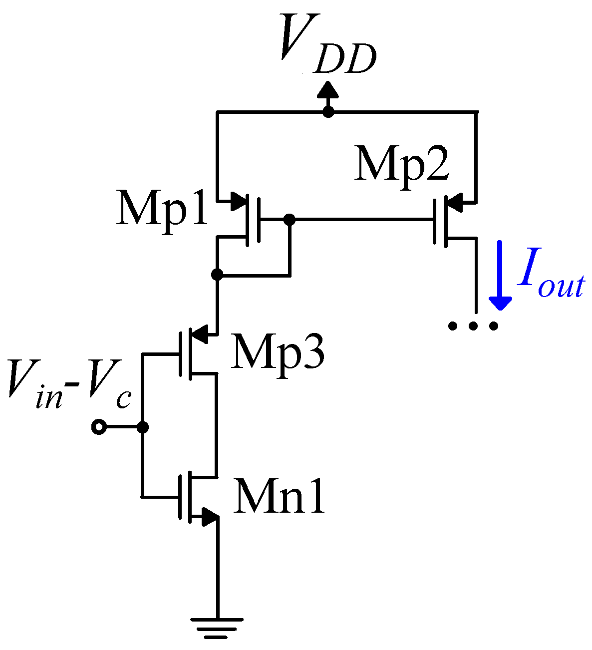
Figure 35.
An example of a Gaussian function circuit based on an exponentiator circuit.
Figure 35.
An example of a Gaussian function circuit based on an exponentiator circuit.
Figure 36.
A different example of a Gaussian function circuit based on an exponentiator circuit.
Figure 36.
A different example of a Gaussian function circuit based on an exponentiator circuit.
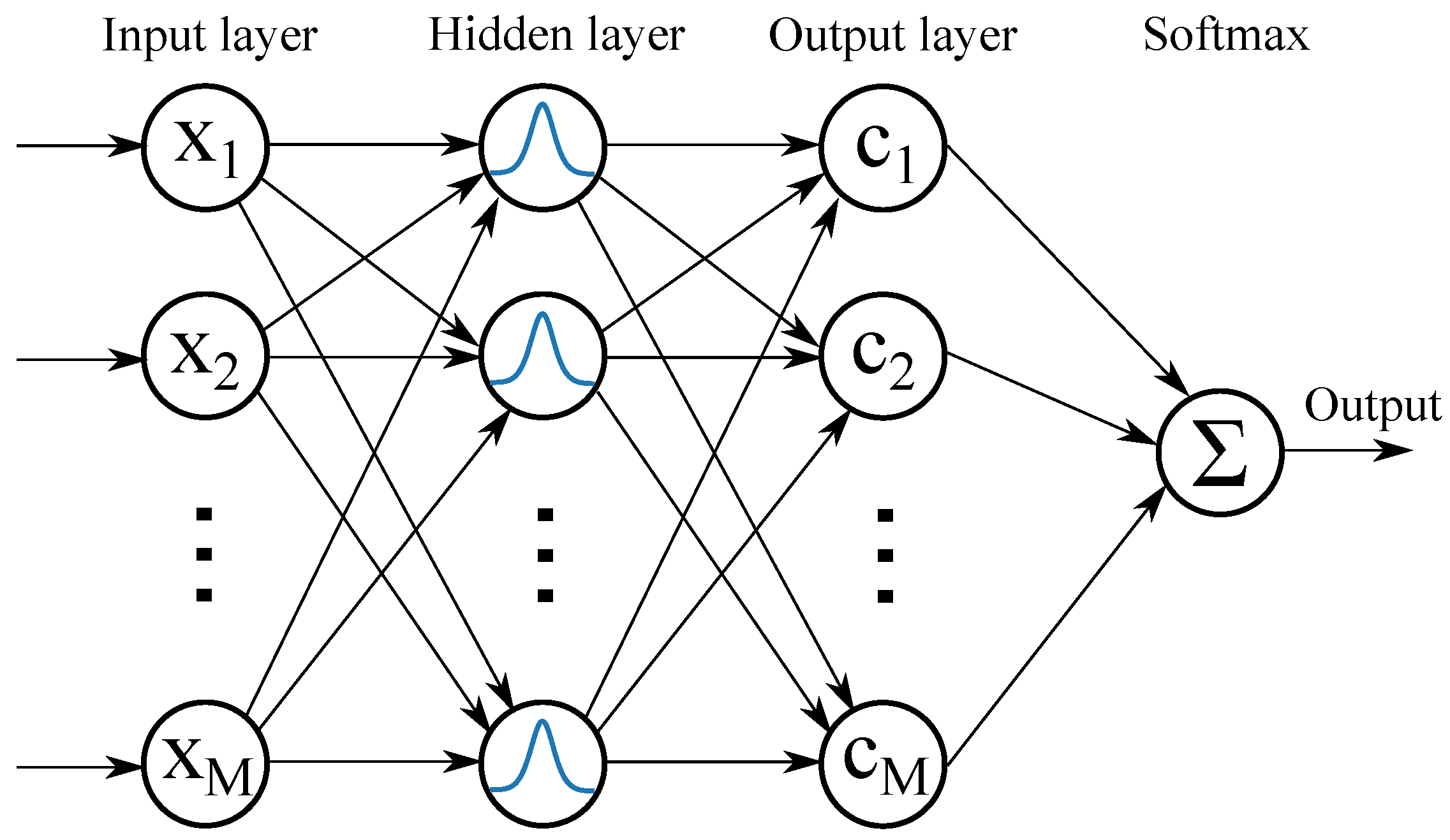
Figure 37.
A generic Radial Basis Function Neural Network architecture.
Figure 37.
A generic Radial Basis Function Neural Network architecture.
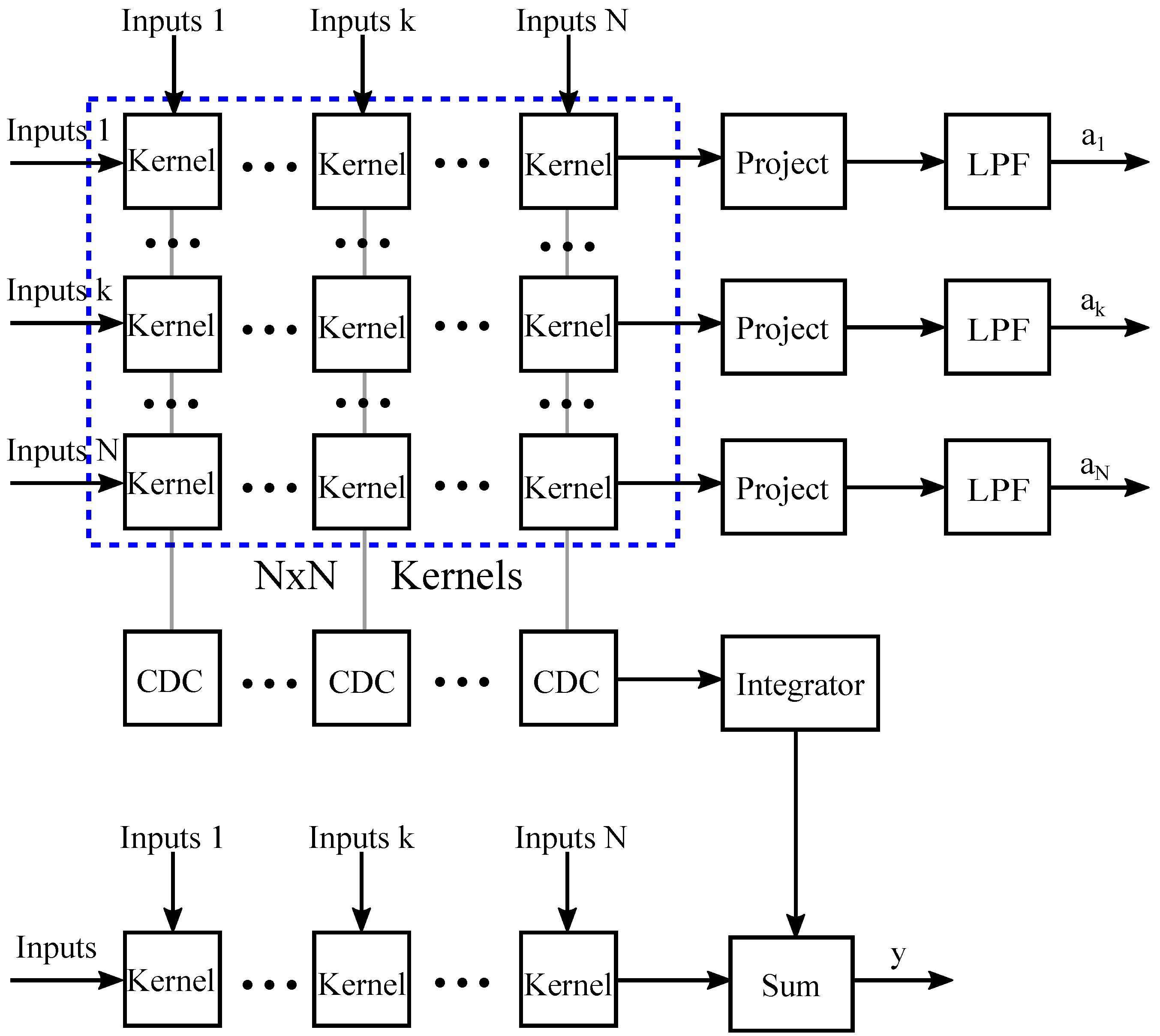
Figure 38.
A hardware friendly implementation of the Support Vector Machine algorithm (learning and classification).
Figure 38.
A hardware friendly implementation of the Support Vector Machine algorithm (learning and classification).
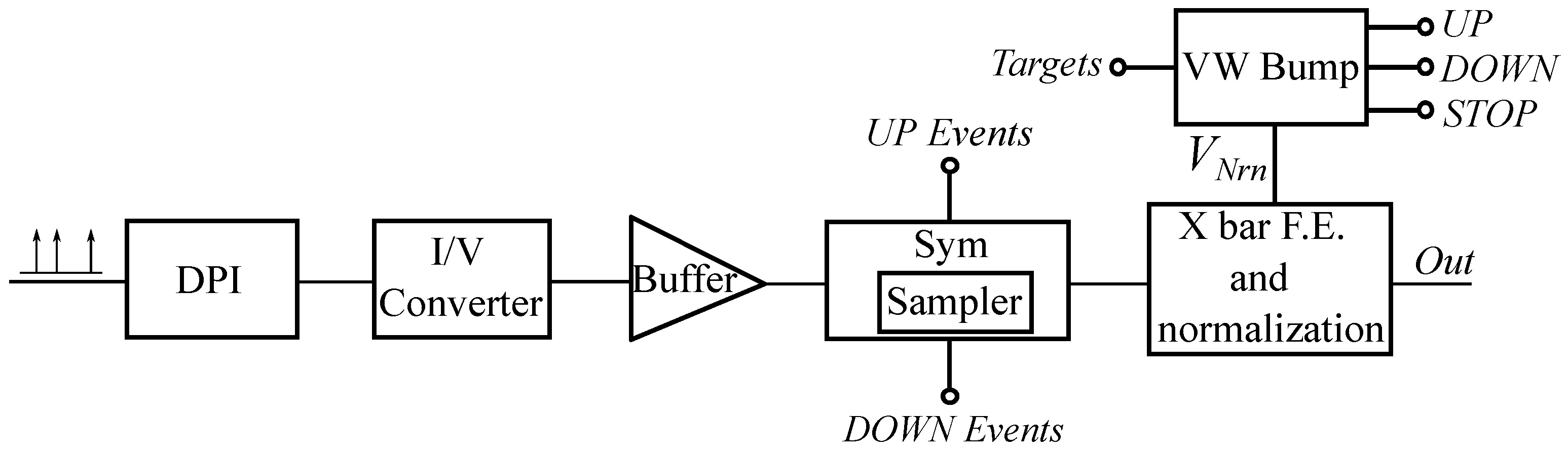
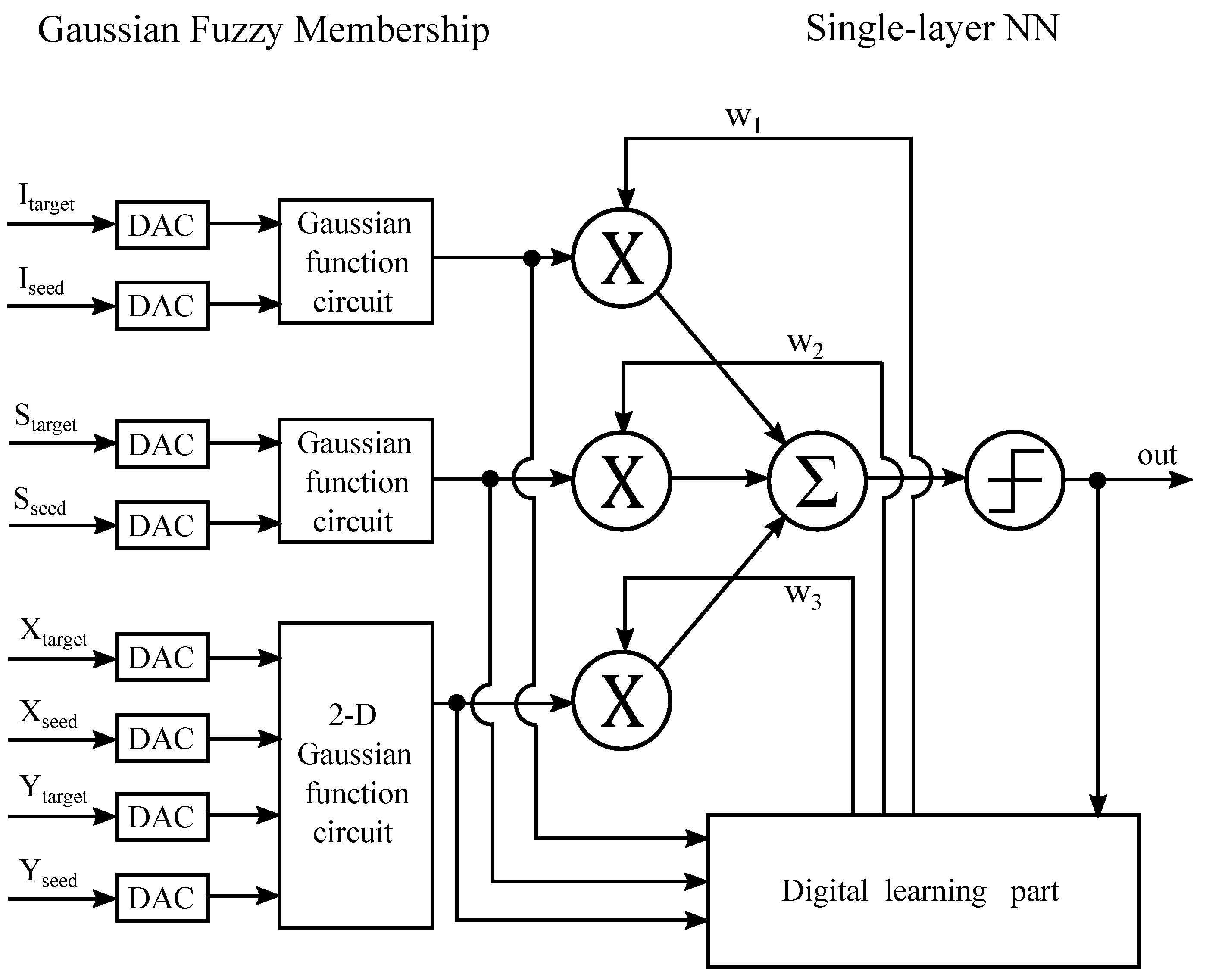
Figure 39.
An example of a neuromorphic network high level architecture based on the VW Bump.
Figure 39.
An example of a neuromorphic network high level architecture based on the VW Bump.
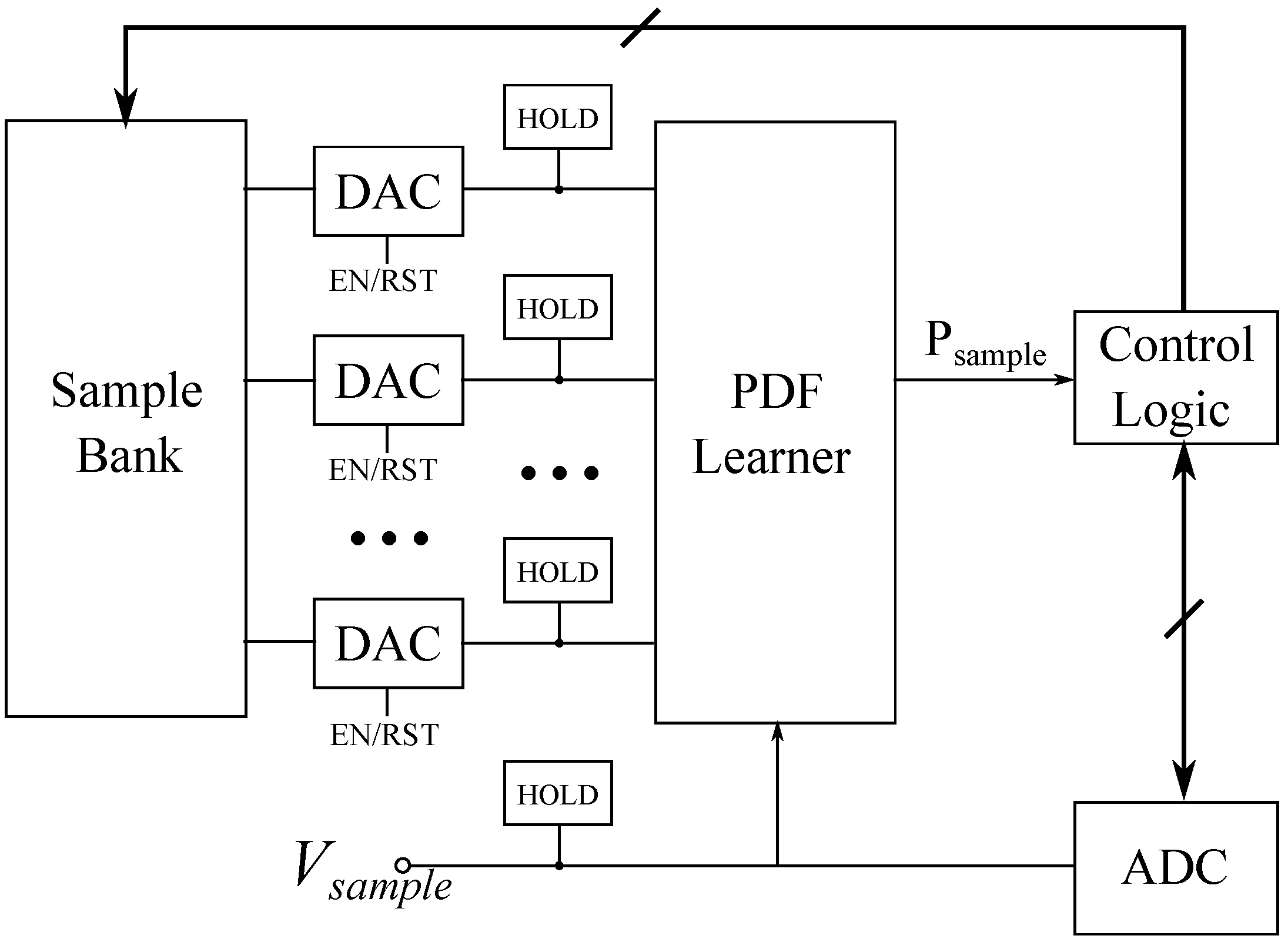
Figure 40.
A mixed-mode anomaly detection system.
Figure 40.
A mixed-mode anomaly detection system.
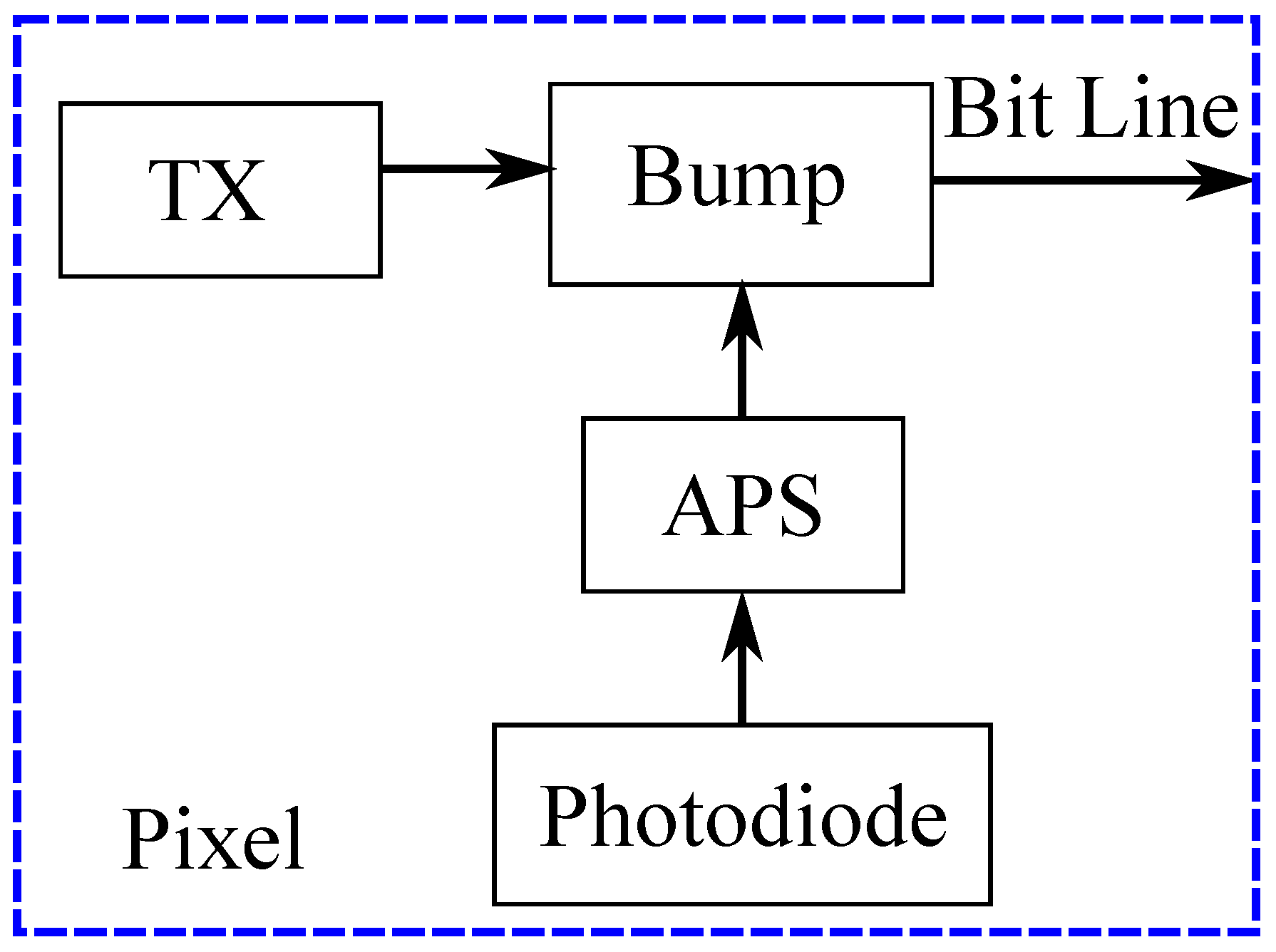
Figure 41.
An edge detection circuit directly connected to a photodiode.
Figure 41.
An edge detection circuit directly connected to a photodiode.
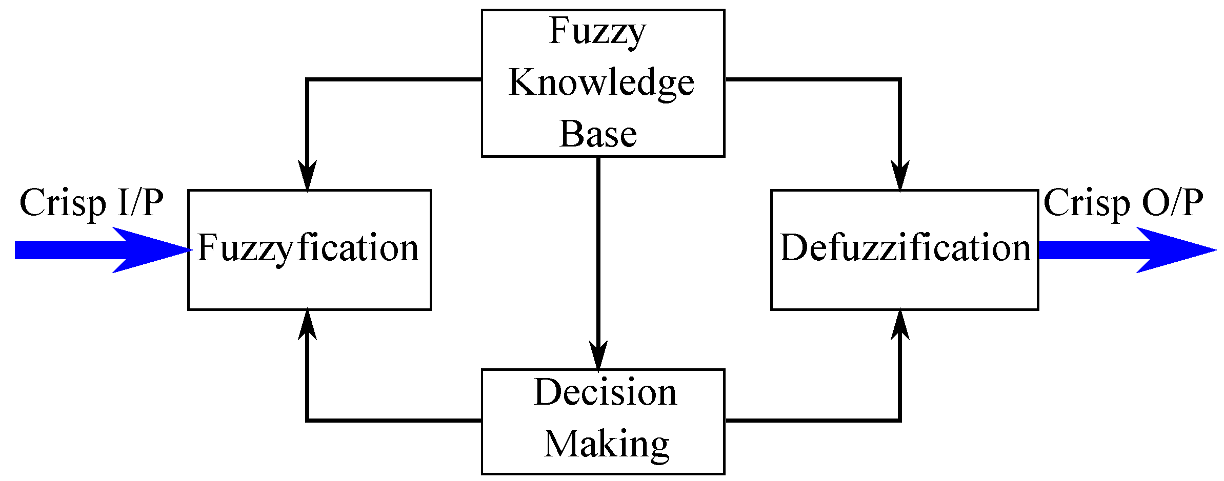
Figure 42.
A generic Fuzzy controller block diagram.
Figure 42.
A generic Fuzzy controller block diagram.
Figure 43.
An example of a shallow Neuro-Fuzzy Radial Basis Function Neural Network.
Figure 43.
An example of a shallow Neuro-Fuzzy Radial Basis Function Neural Network.
Table 1.
Gaussian Function Circuits based on the translinear principle. * For the entire system.
Table 1.
Gaussian Function Circuits based on the translinear principle. * For the entire system.
| Ref. | Technology | Power Consumption | Power Supply | Minimum | Operation Region | No of Transistors |
|---|
| [3] | - | - | 3 V | 325 nA | above threshold | 14 |
| [4] | 180 nm | - | V | 50 nA | sub-threshold | * 600 |
| [25] | 180 nm | 485 nW | V | 10 nA | sub-threshold | 14 |
| [37] | µm | 200 µW | V | 4 nA | sub-threshold | 22 |
| [38] | 180 nm | 350 nW | V | 50 nA | sub-threshold | 31 |
| [39] | 180 nm | * mW | V | µA | above and sub-threshold | 55 |
| [40] | µm | 650 nW | V | 90 nA | sub-threshold | 17 |
| [41] | 180 nm | - | V | 50 nA | sub-threshold | 14 |
| [42] | 180 nm | - | V | 50 nA | sub-threshold | 14 |
| [43] | µm | 843 nW | V | 10 nA | sub-threshold | 22 |
| [43] | µm | µW | V | 40 nA | sub-threshold | 26 |
| [44] | µm | - | V | 10 µA | above threshold | 45 |
| [45] | - | - | - | - | sub-threshold | - |
Table 2.
Bulk-controlled Gaussian Function Circuits. * For the entire System.
Table 2.
Bulk-controlled Gaussian Function Circuits. * For the entire System.
| Ref. | Technology | Power Consumption | Power Supply | Minimum | Operation Region | No of Transistors |
|---|
| [5] | 90 nm | nW | V | 1 nA | Sub-threshold | 11 |
| [6] | | - | 5 V | 2 nA | Sub-threshold | 10 |
| [17] | 180 nm | - | - | 5 nA | Sub-threshold | 20 |
| [18] | 180 nm | - | - | 5 nA | Sub-threshold | 20 |
| [24] | | µW | V | 1 µA | Sub-threshold | 22 |
| [27] | 90 nm | 6 nW | V | 5 nA | Sub-threshold | 10 |
| [32] | 90 nm | nW | V | 3 nA | Sub-threshold | 14 |
| [52] | 180 nm | - | V | 50 nA | Sub-threshold | 15 |
| [53] | 180 nm | - | V | 50 nA | Sub-threshold | 15 |
| [54] | 180 nm | * 50 µW | V | 50 nA | Sub-threshold | 15 |
| [55] | 90 nm | 4 nW | V | 3 nA | Sub-threshold | 10 |
Table 3.
Gaussian Function Circuits using Floating Gate Transistors. * For the entire system.
Table 3.
Gaussian Function Circuits using Floating Gate Transistors. * For the entire system.
| Ref. | Technology | Power Consumption | Power Supply | Minimum | Operation Region | No of Transistors |
|---|
| [7] | 180 nm | 160 nW | V | 35 nA | sub-threshold | 8 |
| [8] | - | - | 10 V | 10 µA | above threshold | - |
| [26] | µm | 214 µW | V | - | above threshold | 5 |
| [61] | µm | 90 µW | V | - | above and sub-threshold | 15 |
| [62] | µm | - | V | - | sub-threshold | 15 |
| [63] | µm | - | V | 200 nA | sub-threshold | 16 |
| [64] | µm | - | - | 5 µA | above threshold | 5 |
| [66] | µm | * 6 mW | 5 V | 100 nA | above or sub-threshold | 6 |
| [67] | µm | - | 5 V | 1 µA | above or sub-threshold | 6 |
| [68] | µm | - | 5 V | 100 nA | above threshold | 6 |
| [69] | 180 nm | 100 µW | V | 10 µA | above threshold | 14 |
Table 4.
Gaussian function circuits built with differential pairs. * Additional current sources or resistors. ** Power consumption for the entire System.
Table 4.
Gaussian function circuits built with differential pairs. * Additional current sources or resistors. ** Power consumption for the entire System.
| Ref. | Technology | Power Consumption | Power Supply | Minimum | Operation Region | No of Transistors |
|---|
| [9] | 180 nm | - | V | - | above and sub-threshold | 4 |
| [10] | | - | 3 V | - | above threshold | 8 |
| [21] | - | - | 10 V | 10 µA | above threshold | * 8 |
| [23] | µm | 105 µW | V | 10 µA | above threshold | 15 |
| [71] | µm | ** 45 mW | 5 V | 100 nA | above threshold | - |
| [72] | 180 nm | ** 20 mW | V | 100 µA | above threshold | 9 |
| [73] | 180 nm | ** mW | V | 100 µA | above threshold | 9 |
| [74] | µm | - | 5 V | 15 µA | above and sub-threshold | * 11 |
| [75] | 180 nm | ** 1 mW | V | - | above threshold | * 8 |
| [76] | | - | 3 V | µA | above threshold | * 8 |
| [77] | 2 µm | - | 3 V | 10 µA | above threshold | 15 |
| [78] | µm | - | 10 V | 5 µA | above threshold | 15 |
| [79] | µm | ** mW | V | 10 µA | above threshold | * 19 |
| [80] | 2 µm | - | 10 V | 50 µA | above threshold | * 10 |
Table 5.
Gaussian Function Circuits using extra components. * Does not include the extra components. ** For the entire system.
Table 5.
Gaussian Function Circuits using extra components. * Does not include the extra components. ** For the entire system.
| Ref. | Technology | Power Consumption | Power Supply | Minimum | Operation Region | No of Transistors |
|---|
| [11] | 180 nm | * nW | V | - | sub-threshold | * 9 |
| [12] | - | ** 2 mW | - | - | sub-threshold | * 6 |
| [15] | 130 nm | ** mW | V | µA | above threshold | *14 |
| [19] | 45 nm | 200 nW | - | - | sub-threshold | 12 |
| [22] | 130 nm | ** mW | 1 V | - | above threshold | * 19 |
| [28] | 180 nm | - | V | 100 nA | sub-threshold | * 11 |
| [31] | 130 nm | ** 496 mW | V | - | above threshold | 12 |
| [33] | 180 nm | 100 µW | 1 V | 10 µA | above threshold | 30 |
| [81] | 130 nm | µW | 2 V | 722 nA | above threshold | * 23 |
| [82] | 130 nm | ** mW | V | µA | above threshold | * 8 |
| [83] | 130 nm | ** 345 mW | V | µA | above threshold | * 8 |
| [84] | 130 nm | ** mW | V | µA | above threshold | * 8 |
| [85] | µm | ** mW | - | 18 µA | above threshold | * 23 |
| [87] | 2 µm | - | 5 V | - | above threshold | - |
| [88] | µm | ** 550 nW | 10 V | - | above threshold | * 4 |
| [89] | µm | 220 µW | V | 9 µA | above threshold | * 14 |
| [90] | 180 nm | µW | 2 V | 5 µA | above threshold | 32 |
| [91] | - | - | 5 V | - | sub-threshold | * 10 |
| [92] | µm | - | 5 V | 4 µA | above threshold | - |
| [93] | µm | - | 5 V | 4 µA | above threshold | - |
| [94] | µm | - | 5 V | 1 µA | above threshold | * 36 |
| [95] | 130 nm | nW | 3 V | 1 nA | sub-threshold | * 14 |
| [96] | 180 nm | 27 µW | V | 2 µA | above threshold | 15 |
| [97] | 3 µm | - | 5 V | nA | above threshold | * 9 |
Table 6.
Gaussian Function Circuits with other implementations. * Additional current sources, resistors or capacitors. ** Power consumption for the entire System.
Table 6.
Gaussian Function Circuits with other implementations. * Additional current sources, resistors or capacitors. ** Power consumption for the entire System.
| Ref. | Technology | Power Consumption | Power Supply | Minimum | Operation Region | No of Transistors |
|---|
| [13] | µm | - | - | - | above threshold | 10 |
| [14] | - | - | - | - | sub-threshold | 12 |
| [16] | µm | - | 5 V | µA | above threshold | * 5 |
| [20] | 180 nm | ** µW per pixel | V | - | above threshold | 8 |
| [29] | 180 nm | µW | 2 V | 3 µA | above threshold | * 22 |
| [30] | µm | - | - | - | above threshold | 10 |
| [65] | 2 µm | - | 3 V | 200 nA | above or sub-threshold | * 4 |
| [98] | 2 µm | - | 3 V | 200 nA | above or sub-threshold | * 4 |
| [99] | 2 µm | ** mW | 5 V | µA | sub-threshold | 14 |
| [100] | 3 µm | - | 5 V | 1 µA | above threshold | 5 |
| [101] | | - | 5 V | - | above threshold | * 4 |
Table 7.
Analog-hardware ML algorithm summary. * tested on LTSpice. ** Estimated.
Table 7.
Analog-hardware ML algorithm summary. * tested on LTSpice. ** Estimated.
| | Implementation | No. of Dimensions | Simulation Level | Area |
|---|
| [4] | SVR algorithm | 2 | Schematic | - |
| [11] | RBF NN | 1 | Chip | mm |
| [12] | RBF NN | 8 | Chip | mm |
| [14] | RBF NN | - | Chip | - |
| [15] | MLP/RBFN | 1280 × 720 pixels | Chip | mm |
| [16] | LVQ or RBF NN | 16 | Chip | - |
| [24] | RBF NN | N | * Layout | 10 µm per bump |
| [28] | RBF NN | 2 | Chip | mm |
| [39] | SOM | 3 | Schematic | ** mm |
| [41] | SVM algorithm | 64 | Chip | - |
| [42] | SVDD algorithm | 2 | Schematic | - |
| [45] | Deep ML engine | 8 | Chip | mm |
| [61] | RBF NN | 2 | Chip | mm |
| [62] | SVM algorithm | 2 | Schematic | - |
| [64] | Vector Quantizer | N | Chip | - |
| [66] | Pattern-matching classifier | 16 | Chip | mm |
| [67] | Similarity evaluation | 4 | Chip | - |
| [68] | Pattern-matching classifier | 16 | Chip | 16,500 µm |
| [81] | RBF NN | - | Chip | 68,400 µm |
| [87] | GRBF NN | N | Schematic | - |
| [94] | RBF NN | 2 | Chip | - |
| [99] | Vector Quantizer | 16 | Chip | mm |
| [101] | RBF NN | 32 | Chip | 1 cm |
Table 8.
Neuromorphic Systems Summary.
Table 8.
Neuromorphic Systems Summary.
| | [17] | [18] | [52] | [53] | [54] |
|---|
| Application | Stop Learning | Error-Triggered Learning Rule | Stochastic Learning | Neuromorphic Computing | EMG |
| Memristive devices | YES | YES | YES | YES | NO |
| Simulation Level | Schematic | Schematic | Schematic | Schematic | Chip |
Table 9.
Smart Sensor Systems Summary.
Table 9.
Smart Sensor Systems Summary.
| | [19] | [20] |
|---|
| Application | Anomaly detection | Edge detection |
| Type of sensor | General | Photodiode |
| Fully Analog | NO | YES |
| Type of Gaussian function | Extra components | Current-mode circuits |
| Power Consumption | 75 µW | µW per pixel |
| Simulation Level | Schematic | Chip |
| Area | - | 225 µm per pixel |
Table 10.
Neuro-fuzzy Systems Summary.
Table 10.
Neuro-fuzzy Systems Summary.
| | Application | Complexity (Fuzzy Rules) | | Area |
|---|
| [21] | Min-Max Network | - | Schematic | - |
| [22] | Processor | 50 | Chip | mm |
| [31] | Neural Perception Engine | - | Chip | 49 mm |
| [71] | Function Approximator | 15 | Chip | 32 mm |
| [72] | Controller | 9 | Chip | mm |
| [74] | Controller | 4 | Chip | - |
| [75] | Function Approximator | 25 | Chip | - |
| [79] | Controller | 25 | Chip | mm |
| [80] | Controller | - | Chip | - |
| [82] | Inference Engine | 8 | Chip | mm |
| [83] | Inference Engine | - | Chip | 50 mm |
| [84] | Inference Engine | 27 | Chip | 50 mm |
| [85] | Controller | 16 | Chip | mm |
| [88] | Controller | 13 | Chip | mm |
Table 11.
Gaussian Function Circuits performance summary and comparison. *Additional current sources.
Table 11.
Gaussian Function Circuits performance summary and comparison. *Additional current sources.
| Ref. | Category | Power Consumption | Power Supply | Minimum | Operation Region | No of Transistors |
|---|
| [5] | Bulk-controlled | 3.9 nW | V | 1 nA | sub-threshold | 11 |
| [27] | Bulk-controlled | 6 nW | V | 5 nA | sub-threshold | 10 |
| [32] | Bulk-controlled | 3.3 nW | V | 3 nA | sub-threshold | 14 |
| [55] | Bulk-controlled | 4 nW | V | 3 nA | sub-threshold | 10 |
| [95] | Extra components | 18.9 nW | 3 V | 1 nA | sub-threshold | * 14 |
Table 12.
Gaussian Function Circuits performance summary and comparison. * Power consumption for the entire System.
Table 12.
Gaussian Function Circuits performance summary and comparison. * Power consumption for the entire System.
| Ref. | Category | Power Consumption | Power Supply | Minimum | Operation Region | No of Transistors |
|---|
| [9] | Differential pair | - | V | - | above and sub-threshold | 4 |
| [20] | Other implementations | * µW per pixel | V | - | above threshold | 8 |
| [26] | Floating gate | 214 µW | V | - | above or sub threshold | 5 |
| [64] | Floating gate | - | - | 5 µA | sub-threshold | 5 |
| [100] | Other implementations | - | 5 V | 1 µA | above threshold | 5 |
Table 13.
Gaussian Function Circuits performance summary and comparison. *Additional current sources.
Table 13.
Gaussian Function Circuits performance summary and comparison. *Additional current sources.
| Ref. | Category | Power Consumption | Power Supply | Minimum | Operation Region | No of Transistors |
|---|
| [5] | Bulk-controlled | 3.9 nW | V | nA | sub-threshold | 11 |
| [6] | Bulk-controlled | - | 5 V | nA | sub-threshold | 10 |
| [55] | Bulk-controlled | 4 nW | V | nA | sub-threshold | 10 |
| [95] | Extra components | nW | 3 V | nA | sub-threshold | * 14 |
| [97] | Extra components | - | 5 V | nA | above or sub-threshold | * 9 |


