Article

Ultralow Voltage FinFET- Versus TFET-Based STT-MRAM Cells for IoT Applications

1
Department of Computer Engineering, Modeling, Electronics and Systems (DIMES), University of Calabria, 87036 Rende, Italy
2
Instituto de Micro y Nanoelectrónica (IMNE), Universidad San Francisco de Quito (USFQ), Quito 170901, Ecuador
3
Dipartimento di Ingegneria dell’Informazione (DII), University of Pisa, 56122 Toscana, Italy
*
Author to whom correspondence should be addressed.
Electronics 2021, 10(15), 1756; https://doi.org/10.3390/electronics10151756
Submission received: 6 July 2021 / Revised: 14 July 2021 / Accepted: 20 July 2021 / Published: 22 July 2021

Abstract

:
Spin-transfer torque magnetic tunnel junction (STT-MTJ) based on double-barrier magnetic tunnel junction (DMTJ) has shown promising characteristics to define low-power non-volatile memories. This, along with the combination of tunnel FET (TFET) technology, could enable the design of ultralow-power/ultralow-energy STT magnetic RAMs (STT-MRAMs) for future Internet of Things (IoT) applications. This paper presents the comparison between FinFET- and TFET-based STT-MRAM bitcells operating at ultralow voltages. Our study is performed at the bitcell level by considering a DMTJ with two reference layers and exploiting either FinFET or TFET devices as cell selectors. Although ultralow-voltage operation occurs at the expense of reduced reading voltage sensing margins, simulations results show that TFET-based solutions are more resilient to process variations and can operate at ultralow voltages (<0.5 V ), while showing energy savings of 50% and faster write switching of 60%.

1. Introduction

Spin-transfer torque magnetic random access memory (STT-MRAM) is an attractive solution for on-chip non-volatile memories with zero standby power [1,2,3,4,5,6,7]. Thanks to the inherent non-volatility, compatibility with CMOS processes, relatively large endurance and, in particular, small area footprint and ability to operate at relatively low voltages, STT-MRAM has become a key memory candidate for future Internet of Things (IoT) applications, where energy-efficiency is a highly sought-after feature [1,8]. Despite these favorable properties, a compatible technology is needed to realize STT-MRAMs working at ultralow operating voltages (i.e., below 0.5 V), as required for low-cost tightly constrained IoT systems [9,10]. Unfortunately, conventional STT-MRAMs based on single-barrier magnetic tunnel junction (SMTJ) present limited voltage scalability, requiring high switching currents for reliable write operations [4,11,12]. In addition, standard transistors based on conventional planar CMOS technologies feature too small on-currents ( I O N ) when operated at reduced voltages. In order to mitigate the above drawback, emerging FinFETs [13,14] or Tunnel-FETs (TFETs) [15,16,17] technologies, along with the double-barrier MTJ (DMTJ) device, can represent effective solutions to design ultralow-power/ultralow-energy STT-MRAMs.
Previous studies [18,19,20,21] have considered FinFET-based STT-MRAM as an alternative to deal with the energy-efficiency limitations of conventional CMOS technology, while also improving write access times in classical SMTJ-based STT-MRAMs. However, high writing currents are still required, and thus a relatively high operating voltage is needed, which limits the overall energy-efficiency of the memory. The studies reported in [12,22] considered a TFET-based technology as access device for STT-MRAM cell, showing that TFET-based cells are more energy efficient than FinFET-based cells. However, this single memory cell study was done under nominal simulations, without taking into account process variability. Another work presented in [4] shows that STT-MRAM based on FinFET technology, along with DMTJ devices with two reference layers, enables lower operating voltage, thanks to the reduced DMTJ switching current as compared to conventional SMTJ, while maintaining sufficiently high thermal stability, so as not to affect data retention time. To further increase the DMTJ-based STT-MRAM energy benefits, advanced FinFET and TFET-based technologies can be exploited. The different sub-threshold conduction behavior of TFET and FinFET has attracted a great attention of several research groups, which have proposed comparative benchmarks based on applications ranging from digital and arithmetic-logic circuits [23,24], to analog blocks [17,25,26] and Static-RAM memory cells [27,28], among the others. Due to inherent device characteristics such as the steep subthreshold slope and the high ON/OFF ratios when operating at low voltages, the collective opinion of the research community is that TFETs have the potential to outperform FinFETs in applications requiring operating supply voltages ( V D D ) below 0.4 V [15].
In the above context, this work investigates STT-MRAM cells based on DMTJ operating at ultralow voltages. In particular, our study was carried out at the memory-bitcell level in which TFET-based DMTJ STT-MRAM bitcells have been benchmarked against their FinFET-based counterparts. Our analysis exploits a state-of-the-art DMTJ Verilog-A compact model [29]. For the simulation of transistors, we used a complementary TFET technology [30] and a predictive technology model (PTM) of 10 n m node FinFET [14], both operating in the sub-threshold voltage regime. All simulations are performed in Cadence Virtuoso environment using the Spectre simulator.
As the main results of our analysis, we demonstrated the suitability of TFET-based STT-MRAM bitcells to design ultralow-power/ultralow-energy memory circuits. When powered at 0.4 V , TFET-based memory bitcells consume less energy (about −50%) and present better performance (about +60%) under write operation, as compared to the FinFET-based implementation. This is achieved while also ensuring higher robustness against process variability.
The remainder of the paper is organized as follows. Section 2 presents the considered device structures for STT-MRAM bitcells. Section 3 provides the simulation and benchmark analysis of FinFET- versus TFET-based STT-MRAM bitcells. Finally, Section 4 summarizes the main conclusions of this work.

2. Ultralow Voltage Transistors and STT-DMTJ

The geometrical structures and main device parameters used in this work, for both transistors (TFET and FinFET) and STT-DMTJ devices, are shown in Figure 1 and in Table 1.

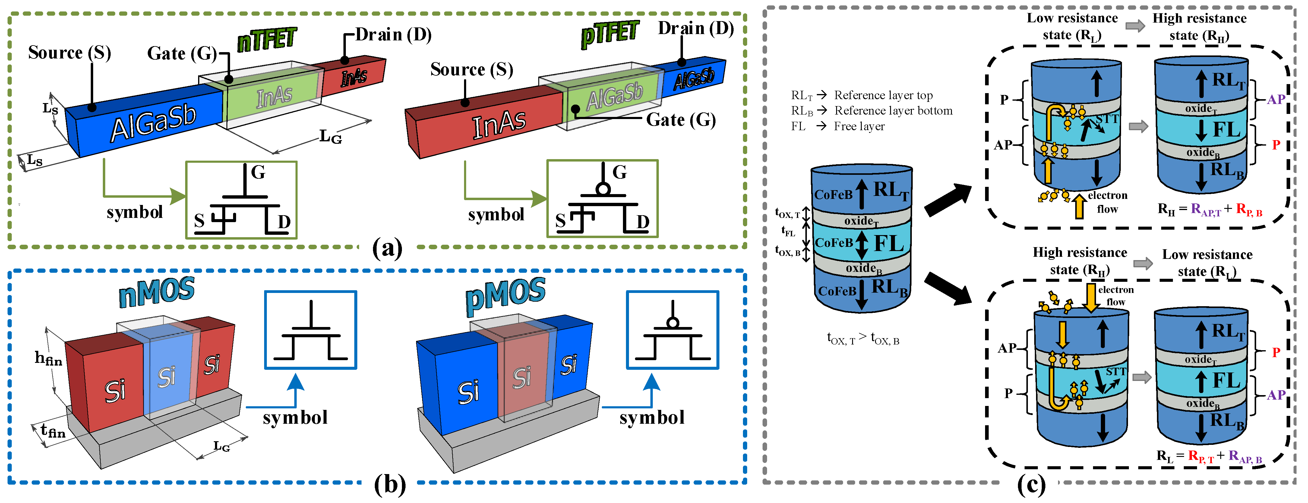
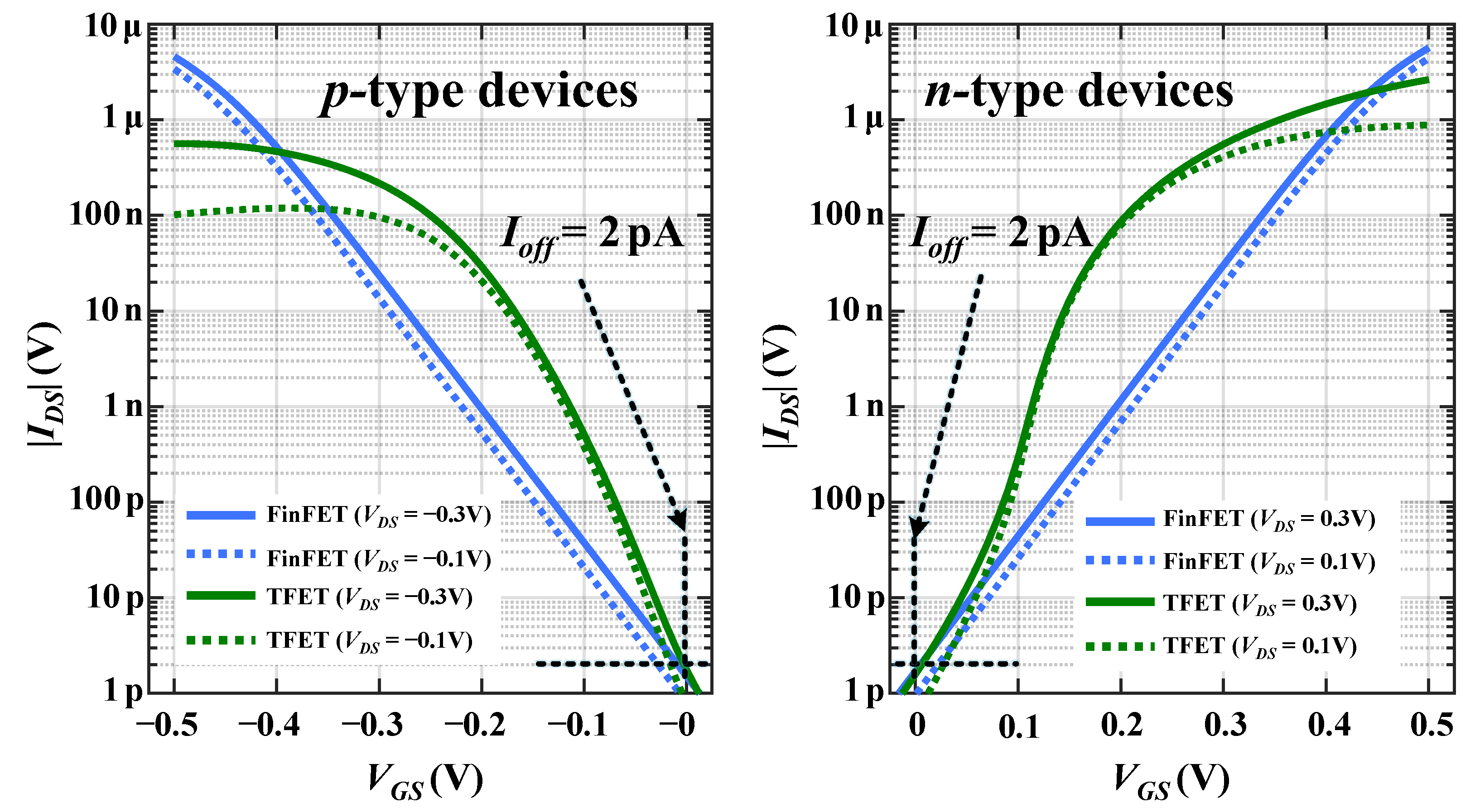
2.1. Tunnel-FET (TFET) and FinFET Structures

The complementary III-V heterojunction TFET nanowires (NWs) proposed by the University of Bologna group [30] depicted in Figure 1a, and the complementary models for 10 n m -node FinFETs deployed by the Arizona State University [14] shown in Figure 1b, are both competitive devices featuring an ultralow-voltage operation capability. In particular, the square cross-section AlGaSb/InAs NWs TFETs ( L S = 7 n m , gate length L G = 20 n m , see Table 1) and the PTM for 10 n m node FinFETs (fin width t f i n = 8 n m , L G = 14 n m ), have the same footprint per device (i.e., 1 TFET NW or 1 FinFET, footprint ∼150 n m 2 ), by assuming a vertical architecture for the TFETs (as the experimental TFET in [31]) and the standard horizontal architecture for the FinFETs. While FinFET models are available for spice simulations, TFET models used in this work are based on I-Vs and C-Vs look-up tables, obtained by performing TCAD simulations of III-V TFET devices, whose parameters were calibrated against NEGF simulations performed by [30]. As for the electrical characteristics, the I D S V G S curves are reported in Figure 2 for both technologies and operation-types. The TFETs exhibit the advantage of a very steep transition due to sub-60 m V /dec sub-threshold swing, but they have to face with unidirectional conduction [32], asymmetric p- and n-operation mode [30], and relatively low on-currents ( I O N ) [16]. In particular, the p-type TFET has four times smaller I O N compared to the n-type counterpart: 420 n A (p-mode) against 1.6 μ A (n-mode) at V D D = 400 m V . At the nominal V D D of 750 m V , the n- and the p-FinFETs feature a threshold voltage, V t h , of 425 m V and −428 m V , an I O N of 44 μ A and −39.5 μ A , and an off-current ( I O F F ) of 5.13 p A and −5.08 p A , respectively. From this perspective, it is obvious that at nominal power supply (750 m V ) they exhibit an extreme advantage with respect to TFETs. However, when operated at a V D D close to 400 m V , their I O N becomes comparable to the one of TFETs ( I O N of 650 n A and −500 n A for n-type and p-type, respectively), and the same absolute I O F F of ∼2 p A is achieved. The comparable performance of nominal TFET and FinFET devices requires a deep analysis in the ultralow-voltage regime, as it is not obvious which is the best candidate to act as a selector for the ultralow power STT-MTJ cell proposed in this work.
Due to the low I O N reported for both TFETs and FinFETs, one single device is not sufficient to act as a proper selector enabling program and erase operations of an STT-MTJ memory cell. Thus, to increase the magnetic device drivability, several parallel nanowires (for the TFETs) or parallel FinFETs have been used to realize a single memory cell. The total multiplier factor (M), has been kept constant for both technologies in order to keep the comparison fair from both area overhead and I O F F (i.e., static power consumption) perspectives. As opposite to most of previous comparative studies, which have considered only nominal device characteristics when benchmarking TFETs and FinFETs, here we also include the device-to-device variability of the threshold voltage, which is a critical issue for circuits operated at extremely reduced V D D levels [33]. The standard deviation ( σ v t h ) is in the 30–40 m V range for scaled node FinFETs [34], according to Perlgrom’s law [35], while no dependable data are available for TFETs (for instance, data in [36] are reported for experimental device with size of the order of hundreds of nanometers). For this reason, the σ v t h has been kept as a free parameter for both technology options. In fact, our goal is to understand the impact of variability at the STT-MRAM bitcell operation level of the different TFET and FinFET characteristics.

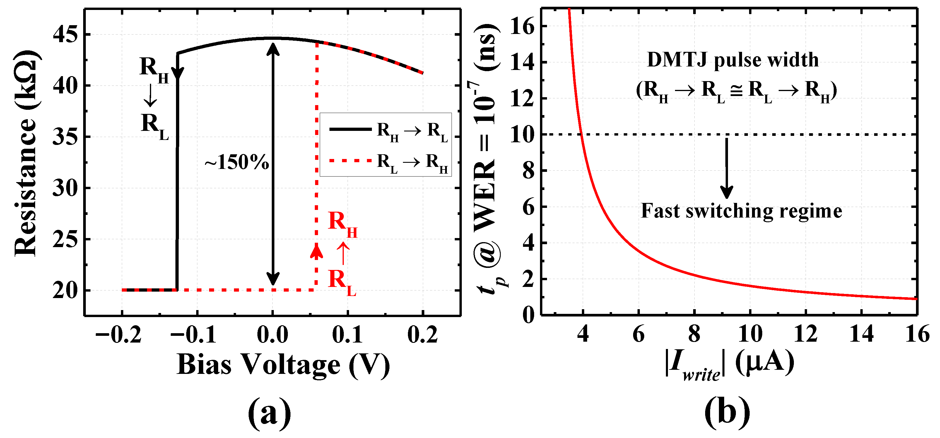
2.2. Double-Barrier Magnetic Tunnel Junction (DMTJ)

As shown in Figure 1c, a perpendicular magnetic anisotropy (PMA) DMTJ device consists of three stacked ferromagnetic (FM) layers separated by two MgO barriers with different thickness ( t O X , T and t O X , B ). The top and bottom FM layers, namely reference layer top ( RL T ) and reference layer bottom ( RL B ), have a fixed magnetization orientation opposite to each other [29]. The remaining FM layer, known as free layer (FL), has a variable magnetization orientation, i.e., parallel (P) or antiparallel (AP) with respect to that of the RL T or RL B layer. Thus, two different device states, which represent the stored data, are possible. Due to the thinner bottom barrier ( t O X , T > t O X , B ) as shown in Figure 1c, the two possible states correspond to two different equivalent resistance values, which derive from two series-connected resistances [4], each one associated with the single oxide barrier. Therefore, the DMTJ resistances in the high and low states ( R H and R L ) can be calculated as R H = R AP , T + R P , B and R L = R P , T + R AP , B , respectively. The low-to-high ( R L R H ) and the high-to-low ( R H R L ) switching transitions are performed by injecting a current, above the critical switching current ( I c 0 ), into the DMTJ. In particular, as shown in Figure 1c, R L R H and R H R L switching transitions arise depending on the direction of the injected current and thus the electron flow.
From Table 1, the DMTJ parameters have been set to match experimental data in terms of I c 0 [11], while also maintaining a reasonable tunnel magnetoresistance (TMR) ratio at 0 V of about 150%. Moreover, to be compatible with the considered transistor devices, the resistance-area product (RA) was set below 10 Ω μ m 2 , which is consistent to the trend reported in [7]. In the following analysis, we have also taken into account the effect of process variability on DMTJ devices, by considering Gaussian-distributed variations, with σ / μ equal to 5% for the cross-section area and to 1% for both the FL thickness ( t F L ) and oxide barrier thicknesses ( t O X , T and t O X , B ) [37,38,39].
Figure 3 shows the electrical characteristics of the DMTJ device. More precisely, Figure 3a shows the typical DC resistance-voltage characteristic, where R L R H and R H R L switching transitions along with the TMR are highlighted. Note that, thanks to the presence of two RLs, we have a symmetric critical current across the R L R H and R H R L switching transitions [29]. This can be graphically appreciated in Figure 3b, where it is shown the switching behavior in terms of write pulse width ( t p ) as function of the write current that ensures a write-error-rate (WER) of 10 7 [4,18].

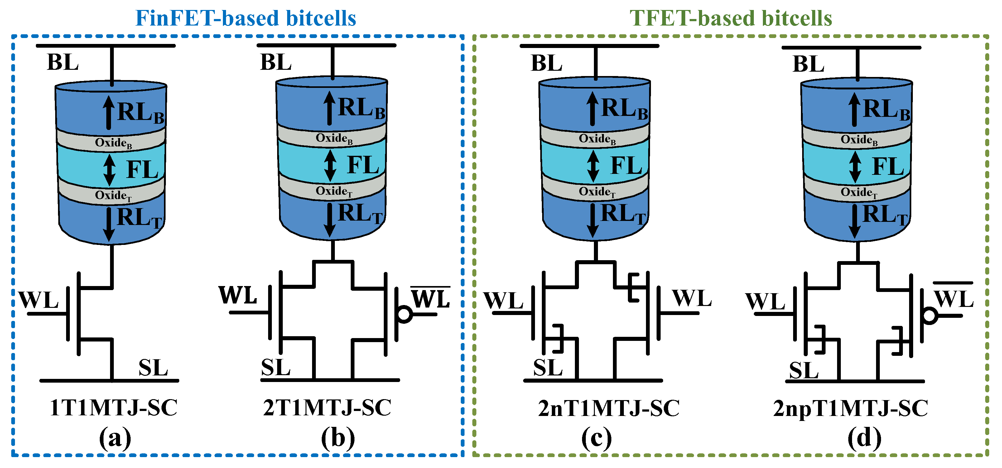
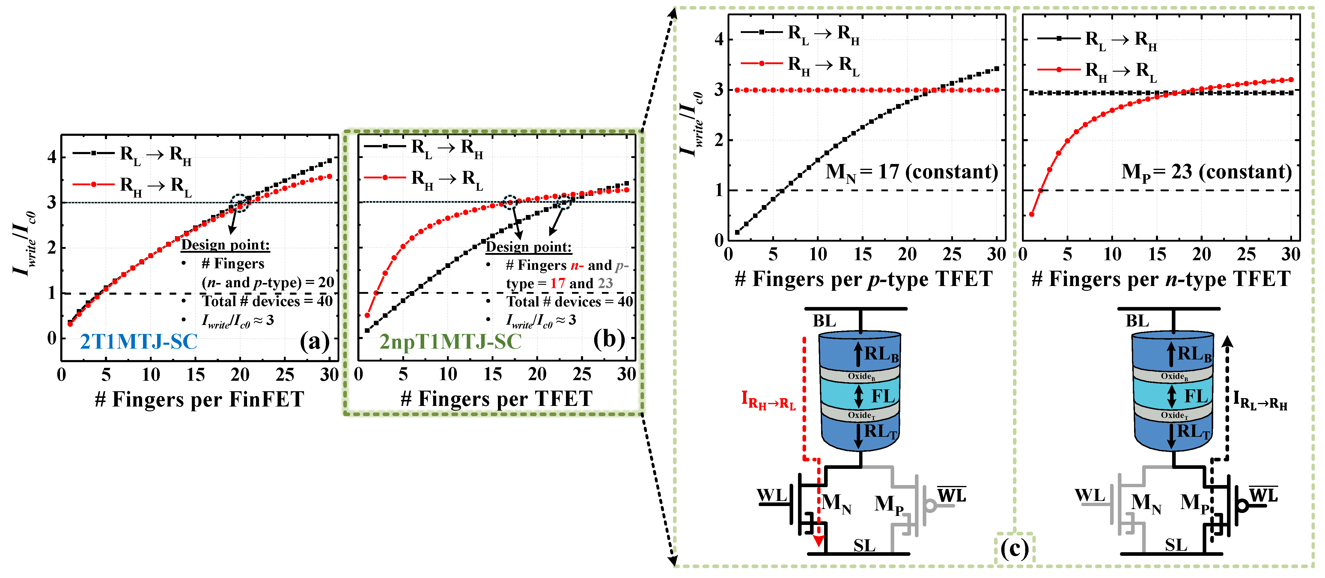
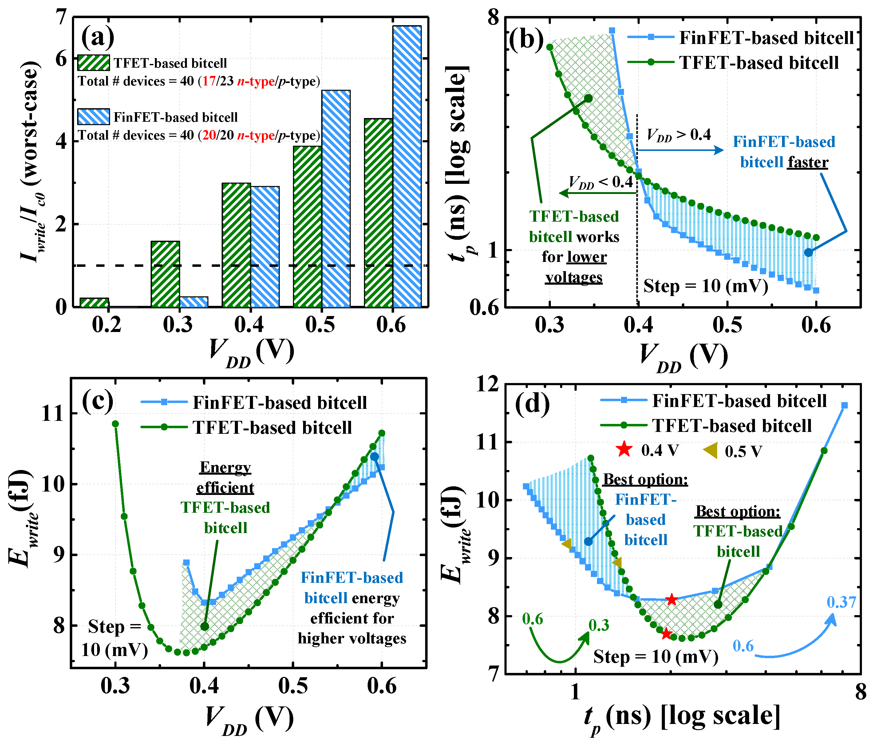
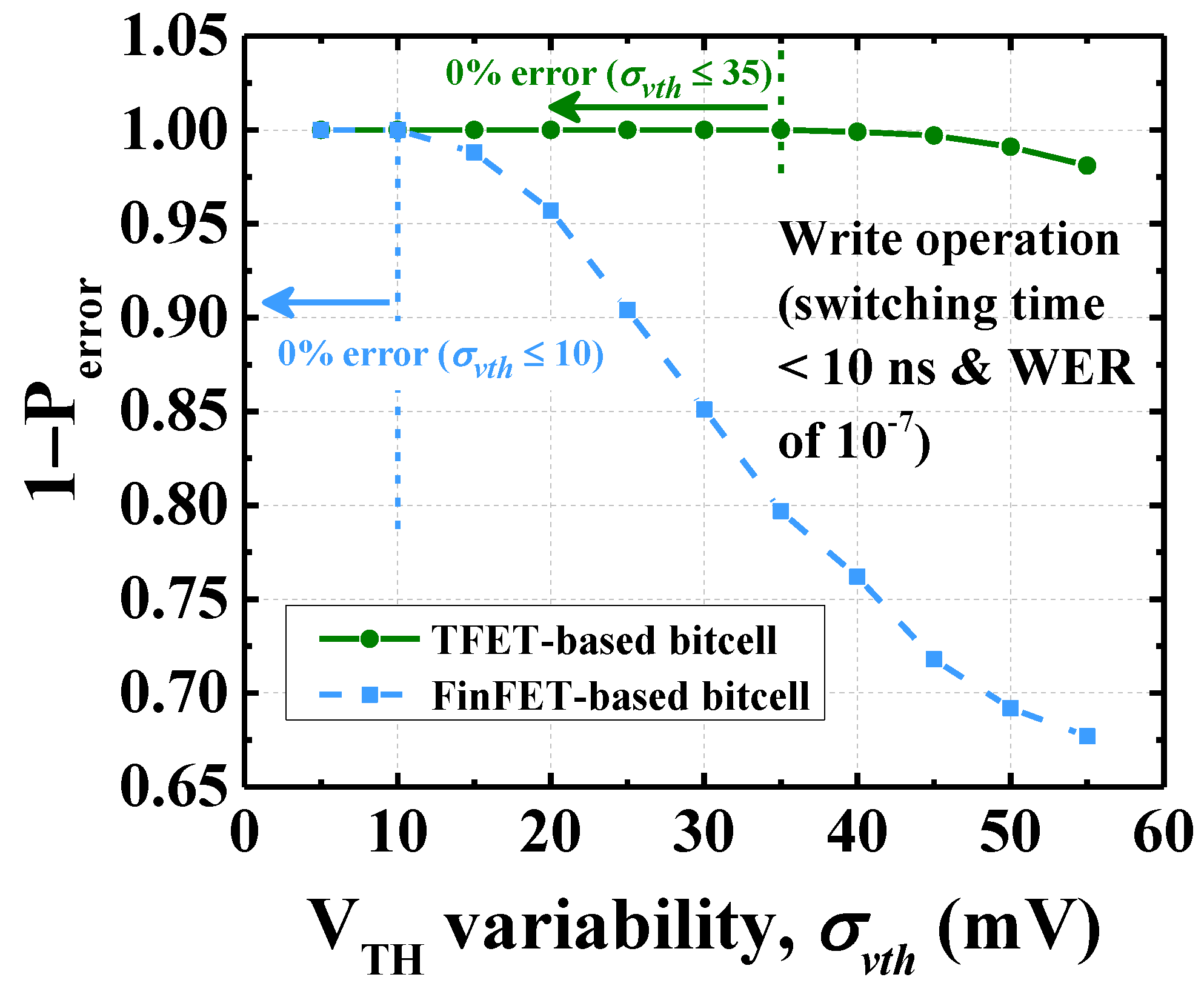
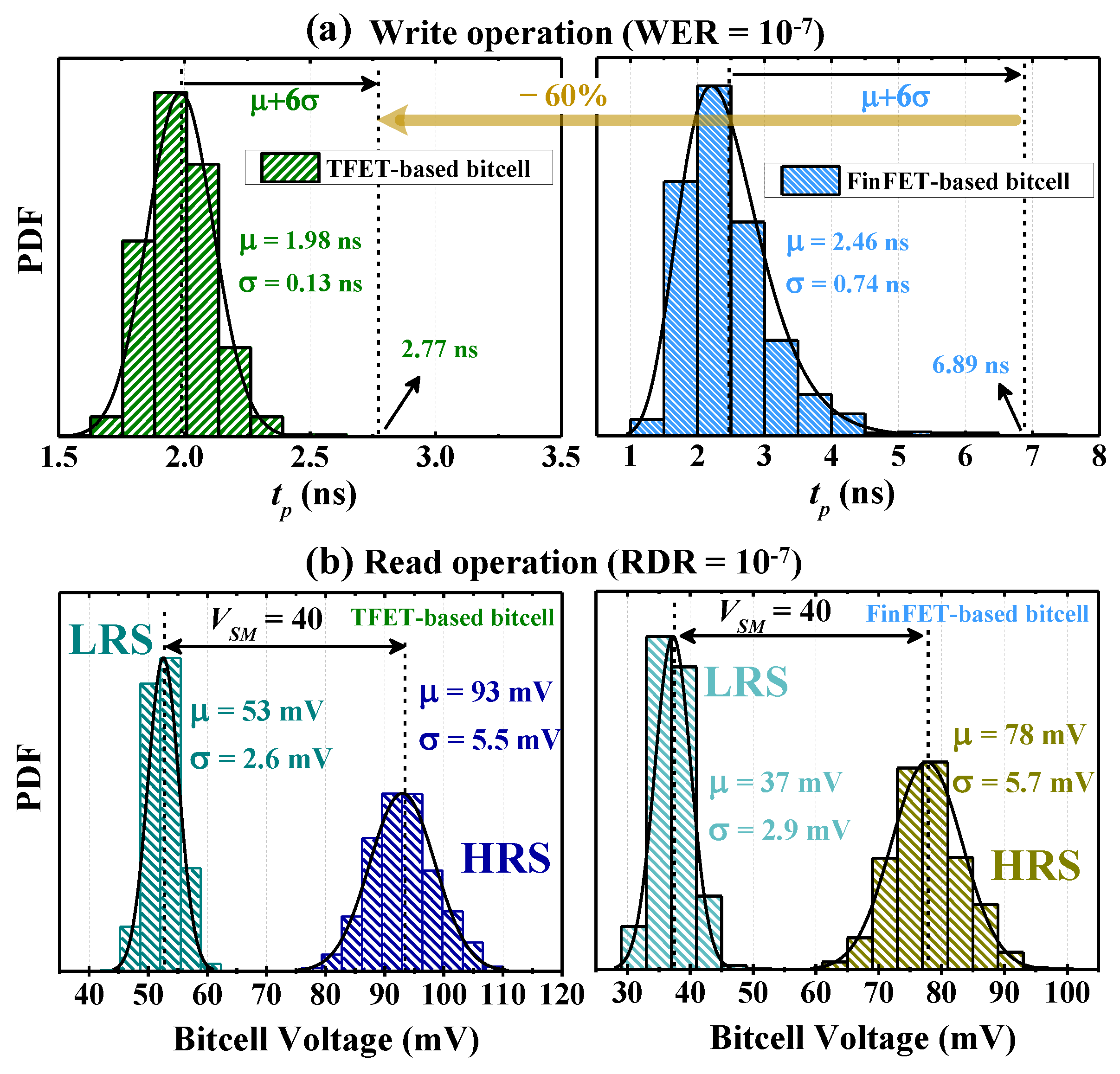
3. STT-MRAM BitCell Simulation and Benchmark

As shown in Figure 4, four bitcell configurations were considered in this work, two based on TFETs and two on FinFETs. All the memory bitcells are in standard connection (SC) configuration, i.e., the RL T of the DMTJ is connected to the access transistor/s. Such a bitcell configuration was demonstrated to be the best option in our previous FinFET-based evaluation [4], and it is here also taken into account for TFET-based bitcells, for the sake of comparison. As shown in Figure 4, the considered FinFET- and TFET-based configurations are: (a) one NMOS-one MTJ in SC (1T1MTJ-SC), and (b) 2T1MTJ with complementary NMOS/PMOS transistors in SC (2T1MTJ-SC), (c) two n-type TFETs-one MTJ in SC (2nT1MTJ-SC), and (d) 2npT1MTJ-SC with complementary n- and p-type TFETs in SC (2npT1MTJ-SC). Note that, owing to the unidirectional behavior of the TFETs, configurations based on a single transistor cannot accomplish the bidirectional writing operation (refer to Figure 1c). Hence, the inclusion of an additional transistor is needed to allow a bidirectional current flow.
As a first step of our analysis, we have evaluated the performance of the bitcells for a supply voltage V D D of 0.4 V . Process variations were initially neglected, while the DMTJ stochastic behavior in the switching time was properly considered. Figure 5 shows the simulation results in terms of the ratio between write current ( I w r i t e ) and I c 0 as functions of the number of parallel-connected devices for both R L R H and R H R L switching transitions. Results in Figure 5 refer to only the best performing bitcell configurations, i.e., 2T1MTJ-SC and 2npT1MTJ-SC for FinFET- and TFET-based bitcells as shown in Figure 5a,b, respectively. The same number of fingers for both access transistor types was considered. As highlighted in Figure 5a,b (refer to the circle with dashed line), to ensure a robust write operation we have chosen a I w r i t e / I c 0 ratio of 3 , which corresponds to a number of fingers of 20/20 and 17/23 for the n-type/p-type FinFETs- and TFET-based bitcell configurations, respectively.
Therefore, we considered a design point for FinFET- and TFET-based bitcells at parity of area and writing current. As of the 2npT1MTJ-SC configuration, we have simulated the I w r i t e / I c 0 as a function of number of fingers per p-type ( M P ) and n-type ( M N ) TFET, while maintaining M N and M P constant, respectively, as shown in Figure 5c. Here, the inherent unidirectional behavior of the TFET devices can be easily appreciated. By fixing M N to a value that ensures the desired I w r i t e / I c 0 ratio of 3 (refer to design point in Figure 5b), we can ensure the same I w r i t e for the R H R L transition independently of M P , as shown in the left part of Figure 5c; a similar behavior occurs when fixing M P .
After choosing the design point in terms of I w r i t e / I c 0 ratio, we extended the TFET- versus FinFET-based bitcell comparison analysis to different supply voltages as shown in Figure 6. Figure 6a shows the I w r i t e / I c 0 ratio referred to the worst-case (i.e., smaller ratio) between switching transitions, where for values > (<) 0.4 V , the FinFET-based (TFET-based) bitcell configuration provides higher write currents. Figure 6b shows that FinFET-based memory cell is the faster solution for V D D > 0.4 V thanks to the the higher I w r i t e / I c 0 (see Figure 6a). However, TFET-based STT-MRAM cell can reliably work for voltages lower than 0.4 V , while achieving faster switching (at the parity of V D D ). Figure 6c shows the average energy ( E w r i t e ), where TFET-based bitcell is more energy efficient for a large range of V D D . Finally, Figure 6d shows the simulation results in the E w r i t e - t p plan, where clearly TFET-based alternative is the most energy-efficient for reduced V D D s and becomes the best option in applications where the time constraints can be relaxed.
To complete our analysis, we have evaluated write and read performance through extensive Monte Carlo simulations by considering device-to-device variability. For both TFET and FinFET devices, it is considered the variability of the threshold voltage. To estimate what is the maximum deviation that can be accepted on each device, we have considered a wide range of σ v t h , from 5 to 55 m V . Figure 7 shows the yield of the write operation (at a WER = 10 7 ) for the fast switching regime (<10 n s ) expressed in terms of error probability ( P error ) ) as function of the threshold voltage variability. The TFET-based bitcell solution shows a yield of ∼100% (i.e., 0% of errors) even for σ v t h larger than 35 m V . It is also clear that the FinFET-based bitcell is not as robust as the TFET-based counterpart, showing that it can only achieve a yield of 100% for σ v t h of 10 m V and below. In light of these results, and for the sake of fair comparison, we have considered a σ v t h of 10 for both TFET- and FinFET-based bitcells in the following analysis.
Figure 8 shows the TFET- and FinFET-based STT-MRAM bitcell Monte Carlo simulation results, while considering the effect of device process variations, for write and read operations ensuring a WER and read disturbance rate (RDR) of 10 7 , at a V D D = 0.4 V and σ v t h = 10 m V . For the write operation (see Figure 8a), in contrast to FinFET-based bitcell, the TFET-based counterpart allows an improvement of about 60%. As for the read operation, we considered a conventional voltage sensing scheme [40], where a fixed read current ( I r e a d ), which assures the target RDR, is forced from the bitline to the sourceline of the bitcell, and the corresponding bitcell/bitline voltage is measured. Figure 8b shows the statistical distribution for the bitcell voltage when the DMTJ is in the low and high resistance states (LRS and HRS, respectively).The voltage sensing margin ( V S M ), which is defined as the difference between bitcell voltages when the DMTJ is in LRS and HRS, is also reported. Although the mean and sigma of the bitcell distributions differ between the considered bitcell configurations, the V S M results are the same for both TFET and FinFET-based bitcells. This is attributed to the constant I r e a d that feeds the bitcells.
Table 2 summarizes writing and reading simulation results for TFET- and FinFET-based bitcells operating at V D D of 0.4 V . Note, the reported data consider Monte Carlo simulations for two values of σ v t h , 10 m V and 35 m V . For results with σ v t h = 10 m V , in contrast to FinFET-based STT-MRAM bitcell, TFET-based alternative allows the E w r i t e to be reduced by about 50%, while also ensuring faster write switching time (60%) at the same bitcell area. This occurs at the cost of worsened read operation in terms of reading sensing margins, V S M , with respect to STT-MRAM bitcells operating at higher V D D s . Although the considered configurations present a relatively small VSM, this issue can be mitigated by adopting several techniques [40,41]. In Table 2, results for σ v t h = 35 m V are also reported, showing that TFET-based bitcell has an increase of 54% and 57% in E w r i t e and t p , 6 σ , respectively, as compared to the case σ v t h of 10 m V . FinFET-based bitcell results for σ v t h = 35 m V were not reported due to the presence of more than 20% write failures as shown in Figure 7.

4. Conclusions

In this work, we explored the impact of using TFETs instead of FinFETs in DMTJ-based STT-MRAM cells. Our study was first performed under nominal conditions at different supply voltages within the subthreshold regime. Then, we extended our performance analysis by considering Monte Carlo simulations taking into account device-to-device process variations on both DMTJ and transistors. Such simulation analysis demonstrated that TFET-based solutions can reliably operate at ultralow-voltages (<0.5 V ). Such benefits are obtained at the cost of reduced voltage sensing margins. In conclusions, the comparative study demonstrated that DMTJ STT-MRAM based on TFETs is the most promising candidate for ultralow-power/ultralow-voltage IoT applications, thanks to its potential in offering lower write energy and switching improved of about 50% and 60%, respectively, as compared to the FinFET-based counterparts.

Author Contributions

Conceptualization, E.G., M.L., R.T., S.S.; formal analysis, E.G., M.L., R.T., S.S.; investigation, E.G., M.L., R.T., S.S.; writing—review and editing, E.G., M.L., R.T., S.S. All authors have read and agreed to the published version of the manuscript.

Funding

This research received no external funding.

Data Availability Statement

The data that support the findings of this study are included within the article.

Conflicts of Interest

The authors declare no conflict of interest.

References

  1. Fong, X.; Kim, Y.; Venkatesan, R.; Choday, S.H.; Raghunathan, A.; Roy, K. Spin-Transfer Torque Memories: Devices, Circuits, and Systems. Proc. IEEE 2016, 104, 1449–1488. [Google Scholar] [CrossRef]
  2. De Rose, R.; Lanuzza, M.; d’Aquino, M.; Carangelo, G.; Finocchio, G.; Crupi, F.; Carpentieri, M. A compact model with spin-polarization asymmetry for nanoscaled perpendicular MTJs. IEEE Trans. Electron Devices 2017, 64, 4346–4353. [Google Scholar] [CrossRef]
  3. Wolf, S.A.; Lu, J.; Stan, M.R.; Chen, E.; Treger, D.M. The Promise of Nanomagnetics and Spintronics for Future Logic and Universal Memory. Proc. IEEE 2010, 98, 2155–2168. [Google Scholar] [CrossRef]
  4. Garzón, E.; De Rose, R.; Crupi, F.; Trojman, L.; Finocchio, G.; Carpentieri, M.; Lanuzza, M. Assessment of STT-MRAMs based on double-barrier MTJs for cache applications by means of a device-to-system level simulation framework. Integr. VLSI J. 2020, 71, 56–69. [Google Scholar] [CrossRef]
  5. Garzón, E.; De Rose, R.; Crupi, F.; Carpentieri, M.; Teman, A.; Lanuzza, M. Simulation Analysis of DMTJ-Based STT-MRAM Operating at Cryogenic Temperatures. IEEE Trans. Magn. 2021, 57, 1–6. [Google Scholar] [CrossRef]
  6. Garzón, E.; De Rose, R.; Crupi, F.; Teman, A.; Lanuzza, M. Exploiting STT-MRAMs for Cryogenic Non-Volatile Cache Applications. IEEE Trans. Nanotechnol. 2021, 20, 123–128. [Google Scholar] [CrossRef]
  7. Apalkov, D.; Khvalkovskiy, A.; Watts, S.; Nikitin, V.; Tang, X.; Lottis, D.; Moon, K.; Luo, X.; Chen, E.; Ong, A.; et al. Spin-Transfer Torque Magnetic Random Access Memory (STT-MRAM). J. Emerg. Technol. Comput. Syst. 2013, 9, 1–35. [Google Scholar] [CrossRef]
  8. Alioto, M. Enabling the Internet of Things: From Integrated Circuits to Integrated Systems; Springer: Cham, Switzerland, 2017. [Google Scholar]
  9. Fassio, L.; Lin, L.; De Rose, R.; Lanuzza, M.; Crupi, F.; Alioto, M. Trimming-Less Voltage Reference for Highly Uncertain Harvesting Down to 0.25 V, 5.4 pW. IEEE J. Solid State Circuits 2021. [Google Scholar] [CrossRef]
  10. Fassio, L.; Lin, L.; De Rose, R.; Lanuzza, M.; Crupi, F.; Alioto, M. A 0.6-to-1.8 V CMOS Current Reference with Near-100% Power Utilization. IEEE Trans. Circuits Syst. II Express Briefs 2021. [Google Scholar] [CrossRef]
  11. Hu, G.; Lee, J.H.; Nowak, J.J.; Sun, J.Z.; Harms, J.; Annunziata, A.; Brown, S.; Chen, W.; Kim, Y.H.; Lauer, G.; et al. STT-MRAM with double magnetic tunnel junctions. In Proceedings of the 2015 IEEE International Electron Devices Meeting (IEDM), Washington, DC, USA, 7–9 December 2015; pp. 26.3.1–26.3.4. [Google Scholar] [CrossRef]
  12. Yamani, S.V.; Rani, N.U.; Vaddi, R. An Energy-Efficient Hybrid Tunnel FET based STT-MRAM Memory Cell Design at Low VDD. Int. J. Electron. 2021, 1–16. [Google Scholar] [CrossRef]
  13. Kuhn, K.J. Considerations for Ultimate CMOS Scaling. IEEE Trans. Electron Devices 2012, 59, 1813–1828. [Google Scholar] [CrossRef]
  14. ASU. Predictive Technology Model (PTM). Available online: http://ptm.asu.edu (accessed on 17 June 2021).
  15. Ionescu, A.; Riel, H. Tunnel field-effect transistors as energy-efficient electronic switches. Nature 2011, 479, 329–337. [Google Scholar] [CrossRef] [PubMed]
  16. Convertino, C.; Zota, C.B.; Schmid, H.; Caimi, D.; Czornomaz, L.; Ionescu, A.M.; Moselund, K.E. A hybrid III–V tunnel FET and MOSFET technology platform. Nat. Electron. 2021, 4, 162–170. [Google Scholar] [CrossRef]
  17. Strangio, S.; Settino, F.; Palestri, P.; Lanuzza, M.; Crupi, F.; Esseni, D.; Selmi, L. Digital and analog TFET circuits: Design and benchmark. Solid State Electron. 2018, 146, 50–65. [Google Scholar] [CrossRef] [Green Version]
  18. Garzón, E.; De Rose, R.; Crupi, F.; Trojman, L.; Lanuzza, M. Assessment of STT-MRAM performance at nanoscaled technology nodes using a device-to-memory simulation framework. Microelectron. Eng. 2019, 215, 111009. [Google Scholar] [CrossRef]
  19. Bhattacharya, A.; Pal, S.; Islam, A. Implementation of FinFET based STT-MRAM bitcell. In Proceedings of the 2014 IEEE International Conference on Advanced Communications, Control and Computing Technologies, Ramanathapuram, India, 8–10 May 2014; pp. 435–439. [Google Scholar] [CrossRef]
  20. Xu, C.; Zheng, Y.; Niu, D.; Zhu, X.; Kang, S.H.; Xie, Y. Impact of Write Pulse and Process Variation on 22 nm FinFET-Based STT-RAM Design: A Device-Architecture Co-Optimization Approach. IEEE Trans. Multi Scale Comput. Syst. 2015, 1, 195–206. [Google Scholar] [CrossRef]
  21. Shafaei, A.; Wang, Y.; Pedram, M. Low write-energy STT-MRAMs using FinFET-based access transistors. In Proceedings of the 2014 IEEE 32nd International Conference on Computer Design (ICCD), Seoul, Korea, 19–22 October 2014; pp. 374–379. [Google Scholar] [CrossRef]
  22. Vani, Y.S.; Rani, N.U.; Vaddi, R. Low Write Energy STT-MRAM Cell Using 2T-Hybrid Tunnel FETs Exploiting the Steep Slope and Ambipolar Characteristics. In Proceedings of the 21st International Symposium, VDAT 2017, Roorkee, India, 29 June–2 July 2017; pp. 398–405. [Google Scholar]
  23. Wang, Z.; Ye, L.; Huang, Q.; Du, K.; Tan, Z.; Wang, Y.; Huang, R. Ultra-Low-Power and Performance-Improved Logic Circuit Using Hybrid TFET-MOSFET Standard Cells Topologies and Optimized Digital Front-End Process. IEEE Trans. Circuits Syst. I Regul. Pap. 2021, 68, 1160–1170. [Google Scholar] [CrossRef]
  24. Strangio, S.; Palestri, P.; Lanuzza, M.; Esseni, D.; Crupi, F.; Selmi, L. Benchmarks of a III-V TFET technology platform against the 10-nm CMOS FinFET technology node considering basic arithmetic circuits. Solid State Electron. 2017, 128, 37–42. [Google Scholar] [CrossRef]
  25. Settino, F.; Lanuzza, M.; Strangio, S.; Crupi, F.; Palestri, P.; Esseni, D.; Selmi, L. Understanding the potential and limitations of tunnel FETs for low-voltage analog/mixed-signal circuits. IEEE Trans. Electron Devices 2017, 64, 2736–2743. [Google Scholar] [CrossRef]
  26. Nogueira, A.D.M.; Agopian, P.G.D.; Simoen, E.; Rooyackers, R.; Claeys, C.; Collaert, N.; Martino, J.A. Impact of gate current on the operational transconductance amplifier designed with nanowire TFETs. Solid State Electron. 2021, 186, 108099. [Google Scholar] [CrossRef]
  27. Lin, Z.; Li, L.; Wu, X.; Peng, C.; Lu, W.; Zhao, Q. Half-Select Disturb-Free 10T Tunnel FET SRAM Cell With Improved Noise Margin and Low Power Consumption. IEEE Trans. Circuits Syst. II Express Briefs 2021, 68, 2628–2632. [Google Scholar] [CrossRef]
  28. Chen, Y.N.; Fan, M.L.; Hu, V.P.H.; Su, P.; Chuang, C.T. Evaluation of Stability, Performance of Ultra-Low Voltage MOSFET, TFET, and Mixed TFET-MOSFET SRAM Cell With Write-Assist Circuits. IEEE J. Emerg. Sel. Top. Circuits Syst. 2014, 4, 389–399. [Google Scholar] [CrossRef]
  29. De Rose, R.; d’Aquino, M.; Finocchio, G.; Crupi, F.; Carpentieri, M.; Lanuzza, M. Compact Modeling of Perpendicular STT-MTJs With Double Reference Layers. IEEE Trans. Nanotechnol. 2019, 18, 1063–1070. [Google Scholar] [CrossRef]
  30. Baravelli, E.; Gnani, E.; Gnudi, A.; Reggiani, S.; Baccarani, G. TFET Inverters With n-/p-Devices on the Same Technology Platform for Low-Voltage/Low-Power Applications. IEEE Trans. Electron Devices 2014, 61, 473–478. [Google Scholar] [CrossRef]
  31. Memisevic, E.; Svensson, J.; Hellenbrand, M.; Lind, E.; Wernersson, L.E. Vertical InAs/GaAsSb/GaSb tunneling field-effect transistor on Si with S = 48 mV/decade and Ion = 10 μA/ μm for Ioff = 1 nA/ μm at Vds = 0.3 V. In Proceedings of the 2016 IEEE International Electron Devices Meeting (IEDM), San Francisco, CA, USA, 3–7 December 2016; pp. 19.1.1–19.1.4. [Google Scholar] [CrossRef] [Green Version]
  32. Morris, D.H.; Vaidyanathan, K.; Avci, U.E.; Liu, H.; Karnik, T.; Young, I.A. Enabling high-performance heterogeneous TFET/CMOS logic with novel circuits using TFET unidirectionality and low-VDD operation. In Proceedings of the 2016 IEEE Symposium on VLSI Technology, Honolulu, HI, USA, 14–16 June 2016; pp. 1–2. [Google Scholar] [CrossRef]
  33. Alioto, M. Ultra-Low Power VLSI Circuit Design Demystified and Explained: A Tutorial. IEEE Trans. Circuits Syst. I Regul. Pap. 2012, 59, 3–29. [Google Scholar] [CrossRef]
  34. Wang, X.; Cheng, B.; Brown, A.R.; Millar, C.; Kuang, J.B.; Nassif, S.; Asenov, A. Interplay Between Process-Induced and Statistical Variability in 14-nm CMOS Technology Double-Gate SOI FinFETs. IEEE Trans. Electron Devices 2013, 60, 2485–2492. [Google Scholar] [CrossRef]
  35. Pelgrom, M.; Duinmaijer, A.; Welbers, A. Matching properties of MOS transistors. IEEE J. Solid State Circuits 1989, 24, 1433–1439. [Google Scholar] [CrossRef]
  36. Huang, Q.; Jia, R.; Chen, C.; Zhu, H.; Guo, L.; Wang, J.; Wang, J.; Wu, C.; Wang, R.; Bu, W.; et al. First foundry platform of complementary tunnel-FETs in CMOS baseline technology for ultralow-power IoT applications: Manufacturability, variability and technology roadmap. In Proceedings of the 2015 IEEE International Electron Devices Meeting (IEDM), Washington, DC, USA, 7–9 December 2015; pp. 22.2.1–22.2.4. [Google Scholar] [CrossRef]
  37. Garzón, E.; de Rose, R.; Crupi, F.; Trojman, L.; Teman, A.; Lanuzza, M. Relaxing Non-Volatility for Energy-Efficient DMTJ Based Cryogenic STT-MRAM. Solid-State Electron. 2021, 184, 108090. [Google Scholar] [CrossRef]
  38. Ohashi, T.; Yamaguchi, A.; Hasumi, K.; Inoue, O.; Ikota, M.; Lorusso, G.; Donadio, G.L.; Yasin, F.; Rao, S.; Kar, G.S. Variability study with CD-SEM metrology for STT-MRAM: Correlation analysis between physical dimensions and electrical property of the memory element. In Metrology, Inspection, and Process Control for Microlithography XXXI; SPIE Advanced Lithography: San Jose, CA, USA, 2017; Volume 10145, p. 101450H. [Google Scholar] [CrossRef]
  39. Ho, C.H.; Panagopoulos, G.D.; Kim, S.Y.; Kim, Y.; Lee, D.; Roy, K. A physics-based statistical model for reliability of STT-MRAM considering oxide variability. In Proceedings of the 2013 International Conference on Simulation of Semiconductor Processes and Devices (SISPAD), Glasgow, UK, 3–5 September 2013; pp. 29–32. [Google Scholar] [CrossRef]
  40. Trinh, Q.K.; Ruocco, S.; Alioto, M. Dynamic Reference Voltage Sensing Scheme for Read Margin Improvement in STT-MRAMs. IEEE Trans. Circuits Syst. I Regul. Pap. 2018, 65, 1269–1278. [Google Scholar] [CrossRef]
  41. Trinh, Q.K.; Ruocco, S.; Alioto, M. Novel Boosted-Voltage Sensing Scheme for Variation-Resilient STT-MRAM Read. IEEE Trans. Circuits Syst. I Regul. Pap. 2016, 63, 1652–1660. [Google Scholar] [CrossRef]
Figure 1. Sketch of the device architecture for: n- and p-type (a) TFETs and (b) FinFET, and (c) STT DMTJ with magnetization orientation at high ( R H ) and low ( R L ) resistance states along with the electron flow for R L R H and R H R L switching.
Electronics 10 01756 g001
Figure 2. Single TFET (1 nanowire) and FinFET (1 fin) transfer characteristics, I D S V G S , for V D S of 0.1 V and 0.3 V redrawn from [17]. TFET and FinFET characteristics are aligned at the same I o f f 2 p A at V D S = 300 m V .
Electronics 10 01756 g002
Figure 3. (a) DC resistance-voltage characteristic, (b) pulse width ( t p ) versus write current ( I w r i t e ) for the DMTJ structure.
Electronics 10 01756 g003
Figure 4. FinFET-based bitcells: (a) one NMOS-one MTJ in standard connection (SC), 1T1MTJ-SC, (b) complementary NMOS and PMOS transistors with one MTJ in SC (2T1MTJ-SC). TFET-based bitcells: (c) two n-type TFETs-one MTJ in SC (2nT1MTJ-SC), (d) complementary n- and p-type TFETs with one MTJ in SC (2npT1MTJ-SC).
Electronics 10 01756 g004
Figure 5. Ratio between write current ( I w r i t e ) and I c 0 as functions of the number of fingers per device for (a) 2T1MTJ-SC, and (b) 2npT1MTJ-SC configurations. (c) I w r i t e / I c 0 as function of number of fingers per p-type ( M P ) and n-type ( M N ) TFET, while maintaining M N and M P constant, respectively.
Electronics 10 01756 g005
Figure 6. TFET- versus FinFET-based bitcell performance comparison in terms of: (a) I w r i t e / I c 0 ratio, (b) write pulse width, t p , at a write-error-rate of 10 7 , (c) average energy, E w r i t e , and (d) E w r i t e versus t p for different supply voltages. The V D D step is 10 m V .
Electronics 10 01756 g006
Figure 7. Yield of write operation for the fast switching regime (<10 n s ) expressed in terms of error probability ( P error ) ) as function of the threshold voltage variability ( σ v t h ) of TFET and FinFET devices. Each point is the result of Monte Carlo simulation with 1000 samples.
Electronics 10 01756 g007
Figure 8. DMTJ-based STT-MRAM bitcell Monte Carlo simulation results for write and read operations ensuring a WER = 10 7 and RDR = 10 7 , respectively. V D D = 0.4 V and σ v t h = 10 m V .
Electronics 10 01756 g008
Table 1. Device parameters and characteristics.
ParameterDescriptionValue
TFET
L G Gate length20  n m
L S Length of nanowire square cross-section n m
t O X Physical oxide thickness (EOT)2.3  n m (1  n m )
FinFET
hfinFin height21  n m
tfinFin width n m
L G Gate length14  n m
t O X Physical oxide thickness (EOT)1.2  n m (0.88  n m )
DMTJ
dMTJ diameter22  n m
t F L FL thickness n m
t O X , T Top barrier thickness0.85  n m
t O X , B Bottom barrier thickness0.4  n m
RAResistance-area product∼7  Ω μ m 2
α Gilbert damping factor0.025
TMRTunnel magnetoresistance ratio at 0 V150%
R H High resistance state at 0 V44.6 k Ω
R L Low resistance state20 k Ω
I c 0 Critical switching current∼3  μ A
Table 2. Summary of writing (WER = 10 7 ) and reading (RDR = 10 7 ) performances for TFET- and FinFET-based bitcells operating at V D D = 0.4 V .
ParameterTFET-Based BitcellFinFET-Based Bitcell
Variation
( σ vth = 10 m V )
Variation
( σ vth = 35 m V )
Variation
( σ vth = 10 m V )
Variation
( σ vth = 35 m V )
V D D ( V )0.4
Area ( n m 2 )6000
t p , 6 σ ( n s )2.774.366.89Cell does not
work *
E w r i t e ( f J )11.317.4422.7
I r e a d ( μ A )1.68
t r e a d ( n s )1
E r e a d ( f J )0.67
V S M ( m V )40
* The cell presents more than 20% of write failures.
Publisher’s Note: MDPI stays neutral with regard to jurisdictional claims in published maps and institutional affiliations.

