Evaluation of Polylactic Acid Polymer as a Substrate in Rectenna for Ambient Radiofrequency Energy Harvesting

 ,
,  , and
, and
Abstract
:1. Introduction
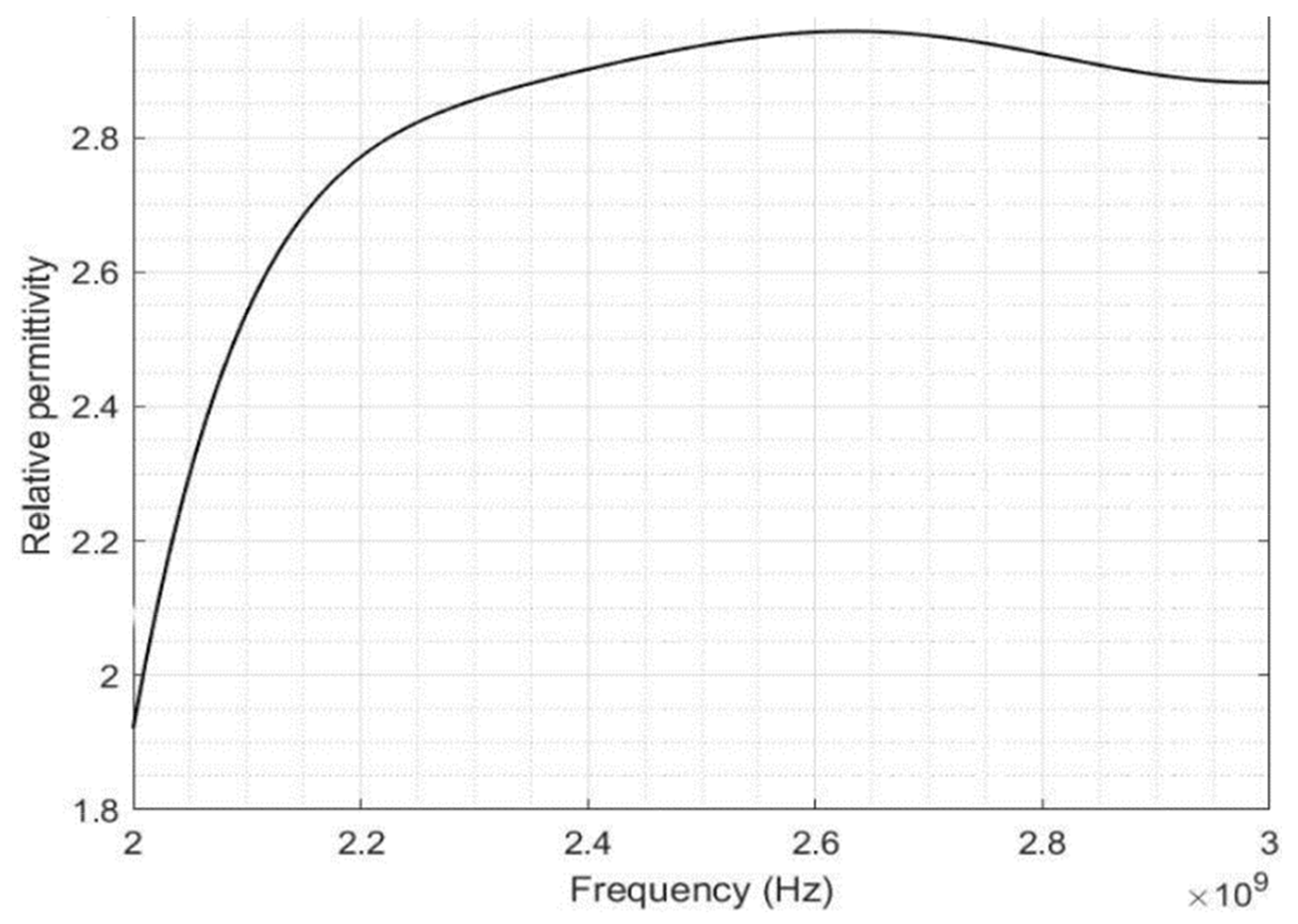
2. Substrate Characterization
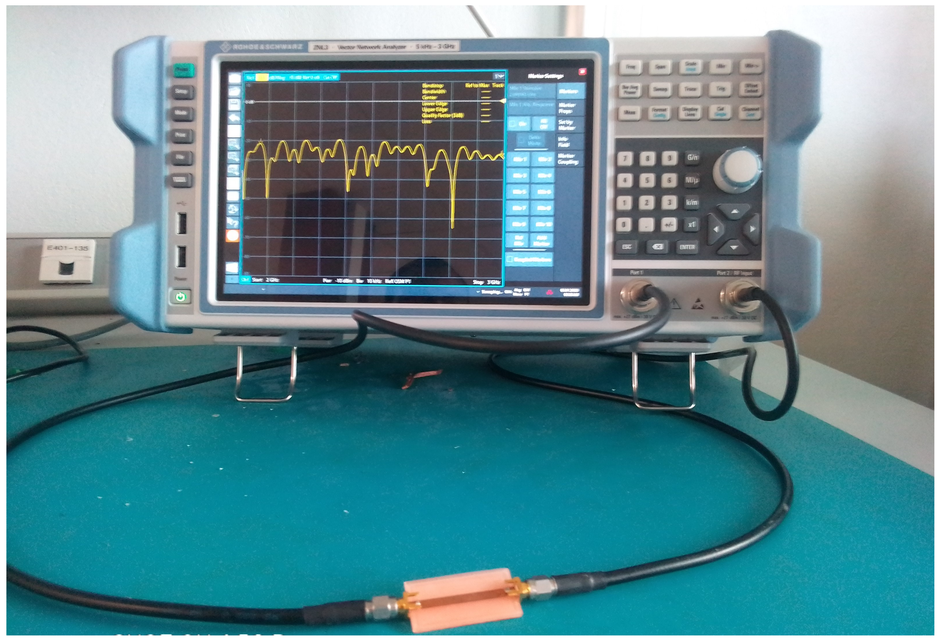
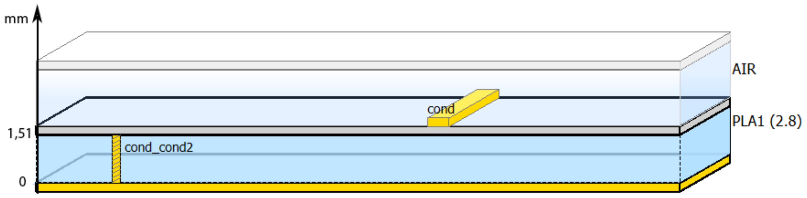
2.1. Deployment of TTL
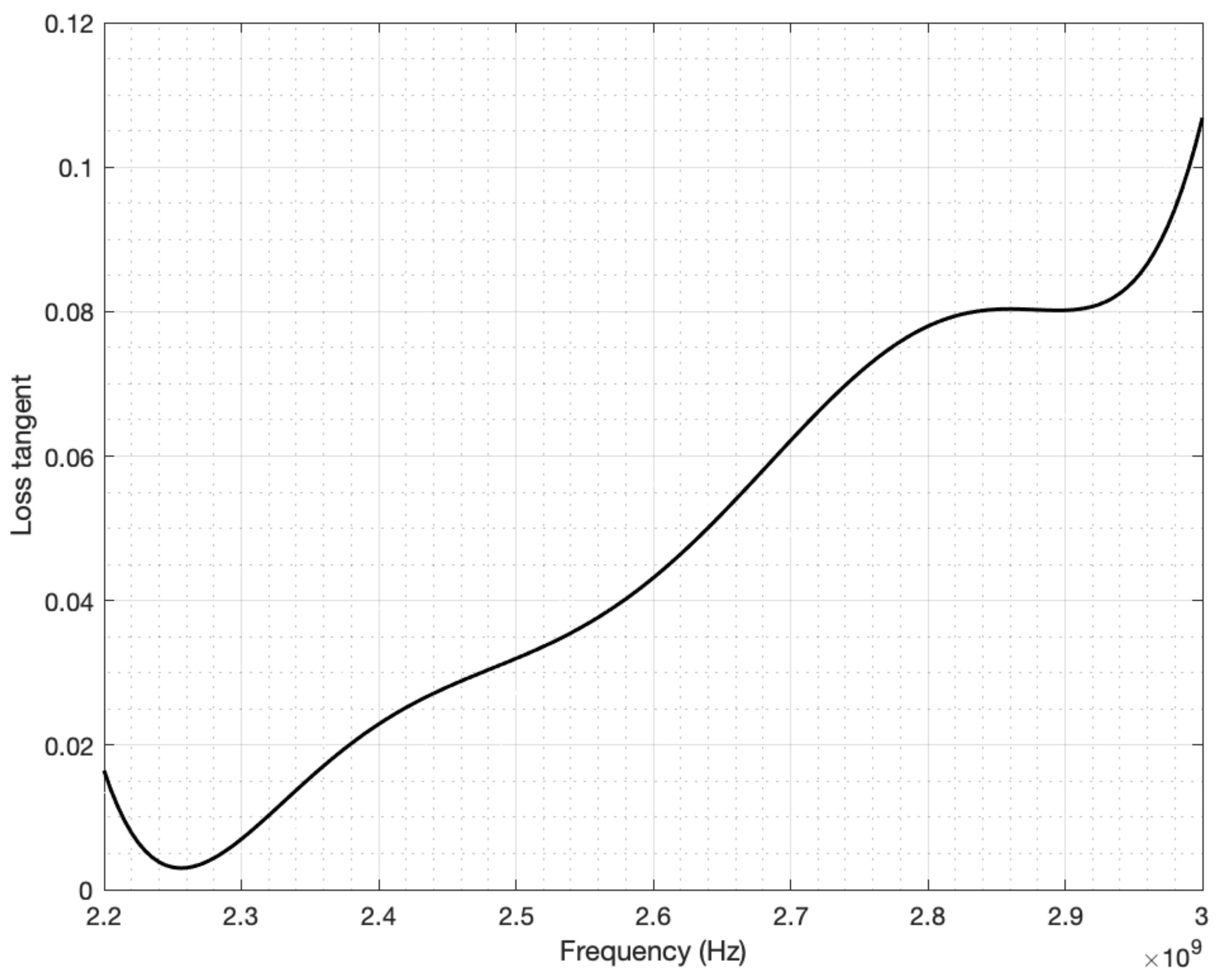
2.2. Measurement Results
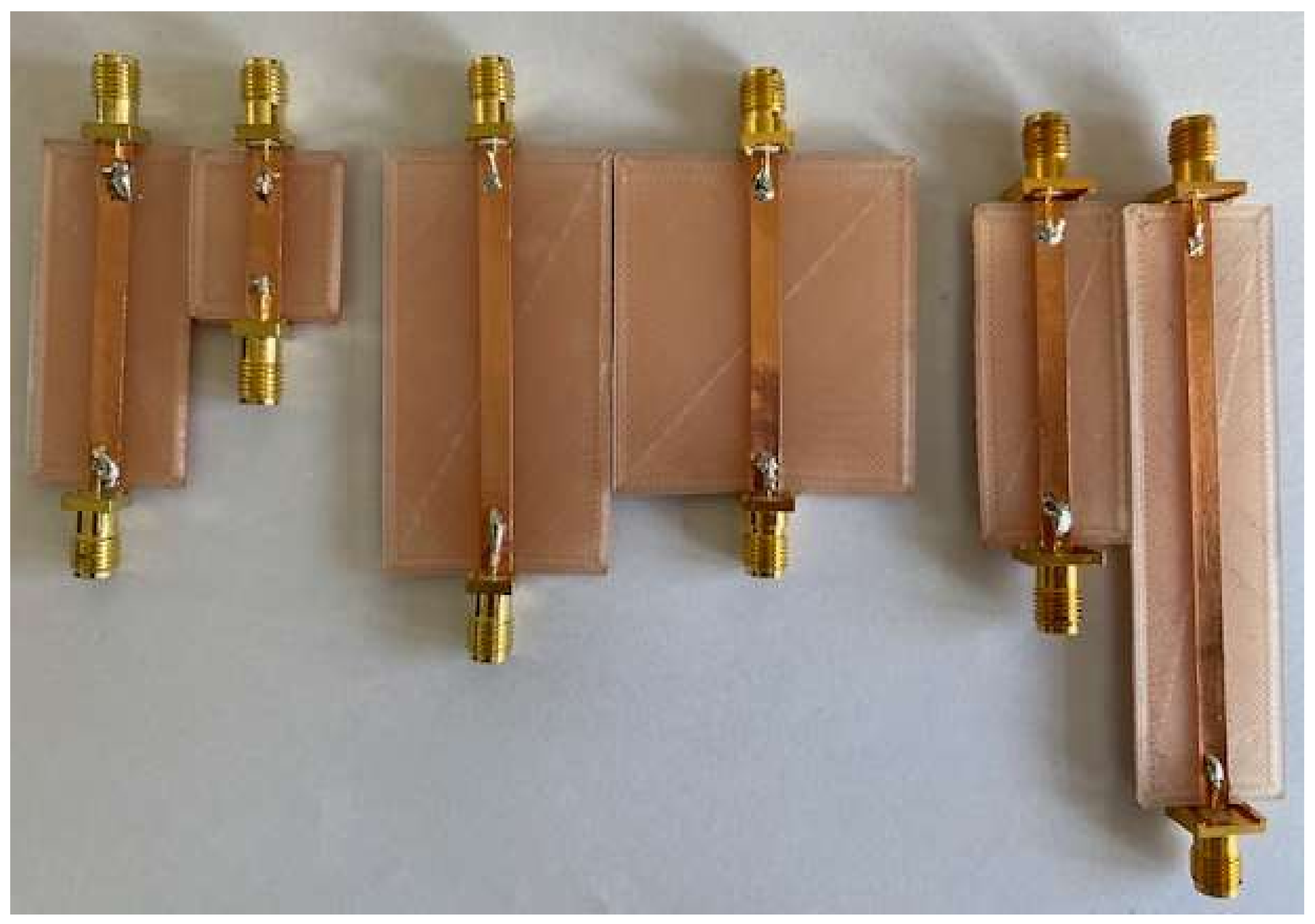
3. Rectenna
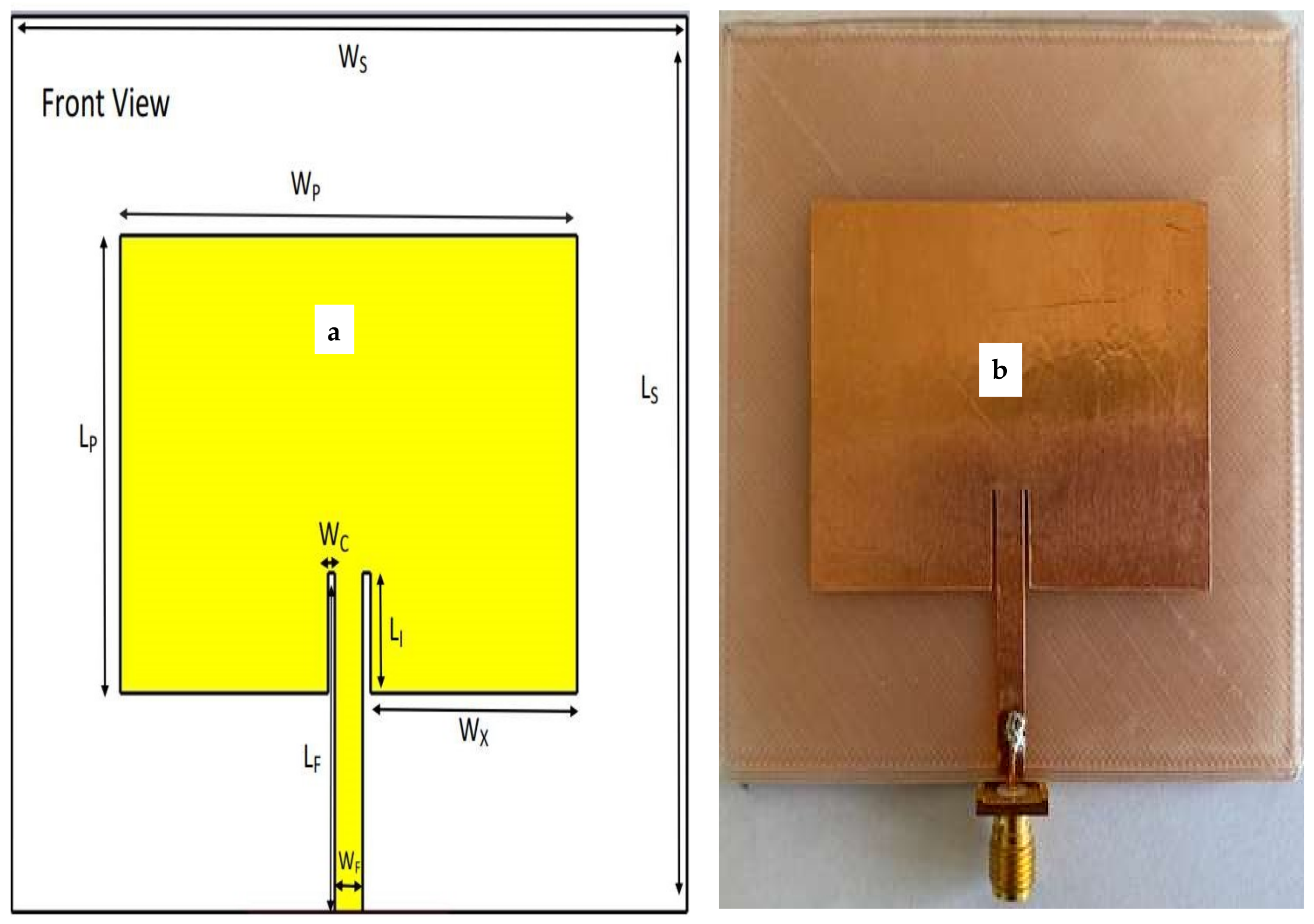
3.1. Antenna Design
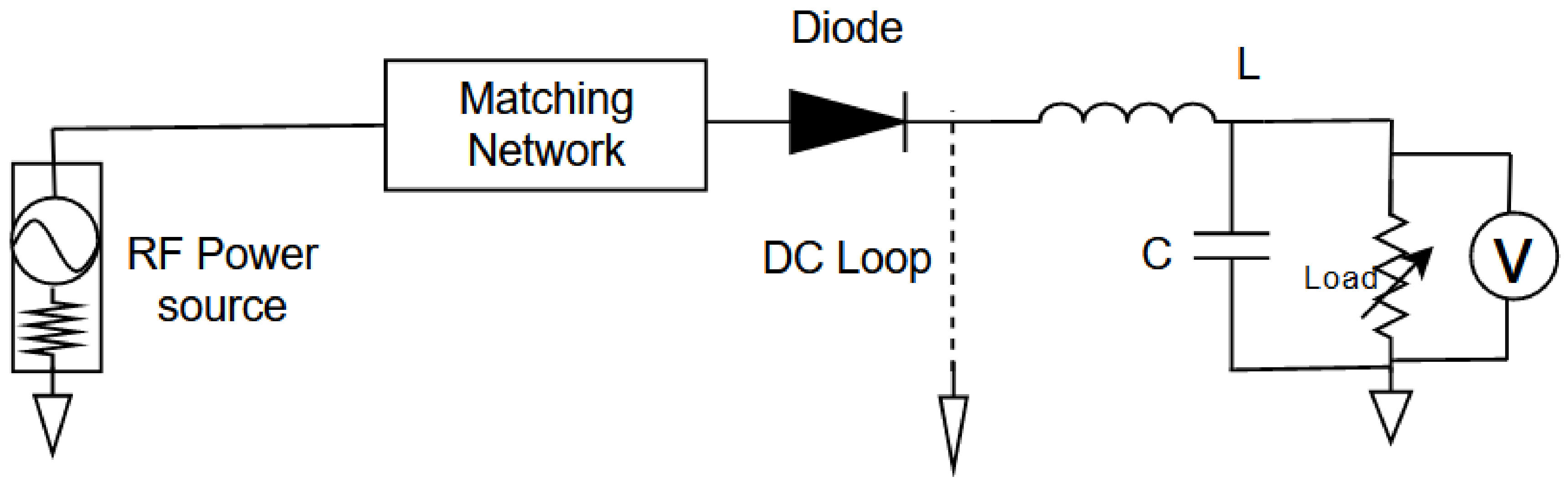
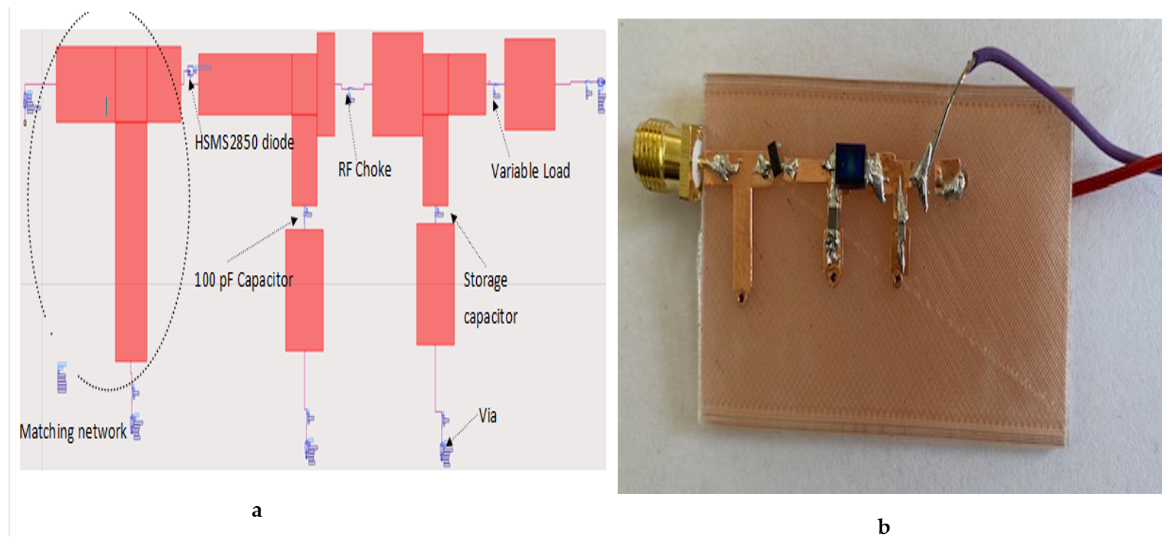
3.2. Rectifier
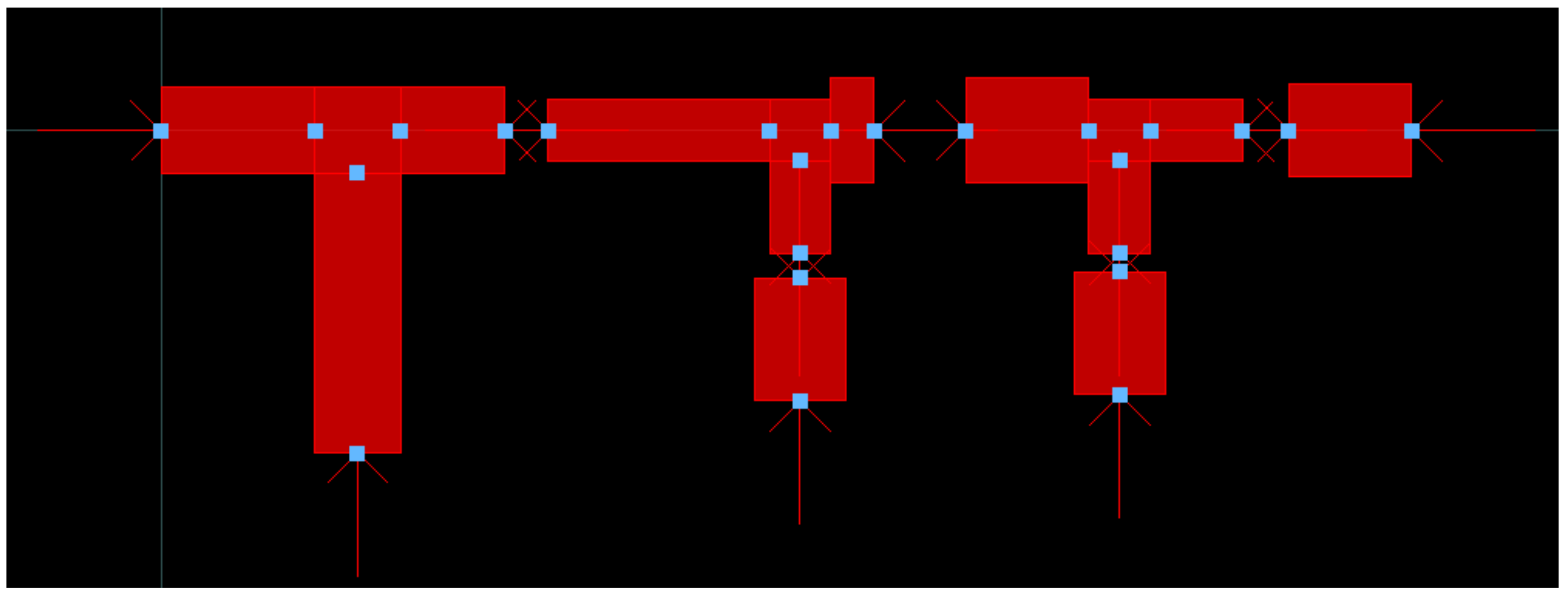
Matching Network Design
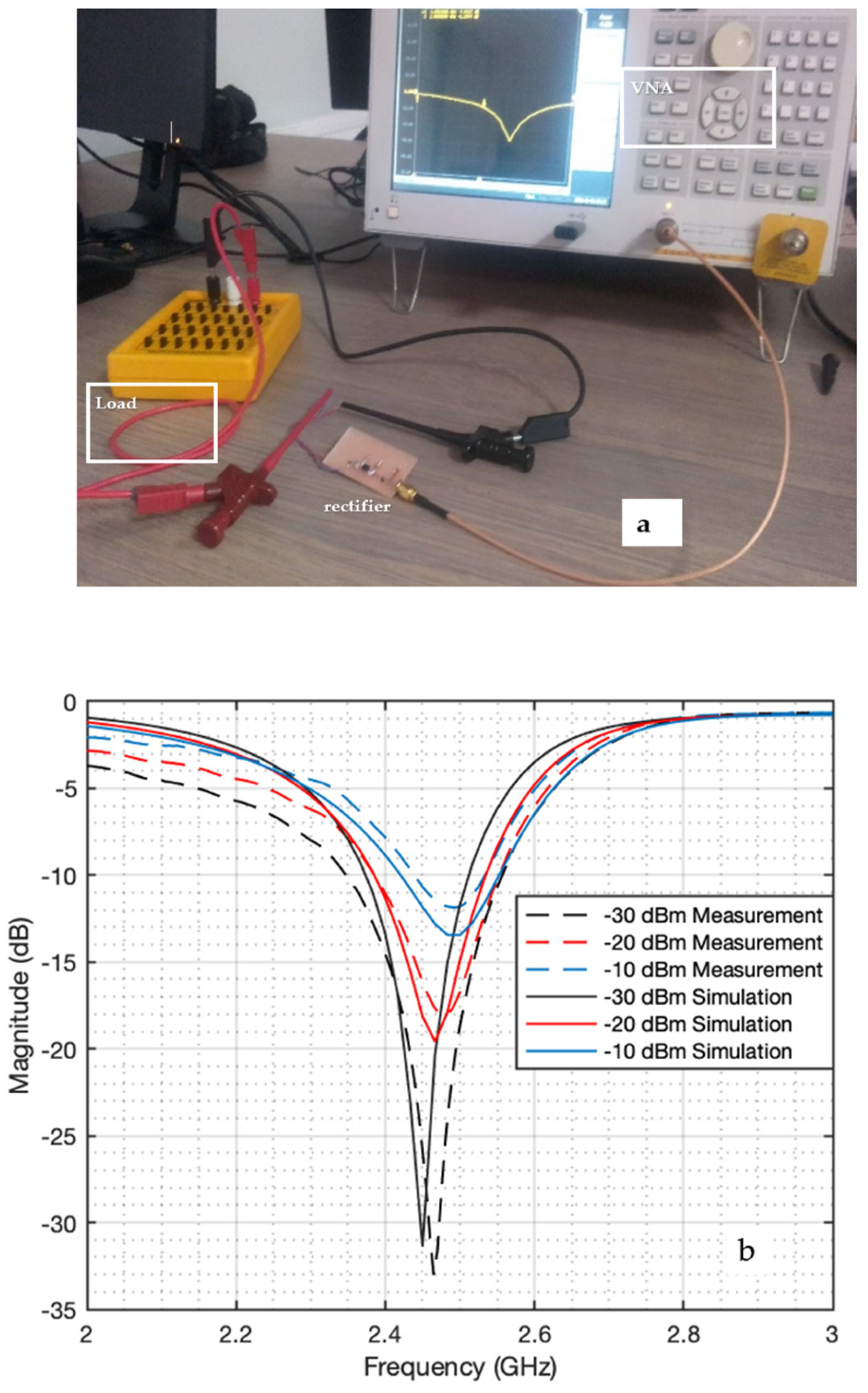
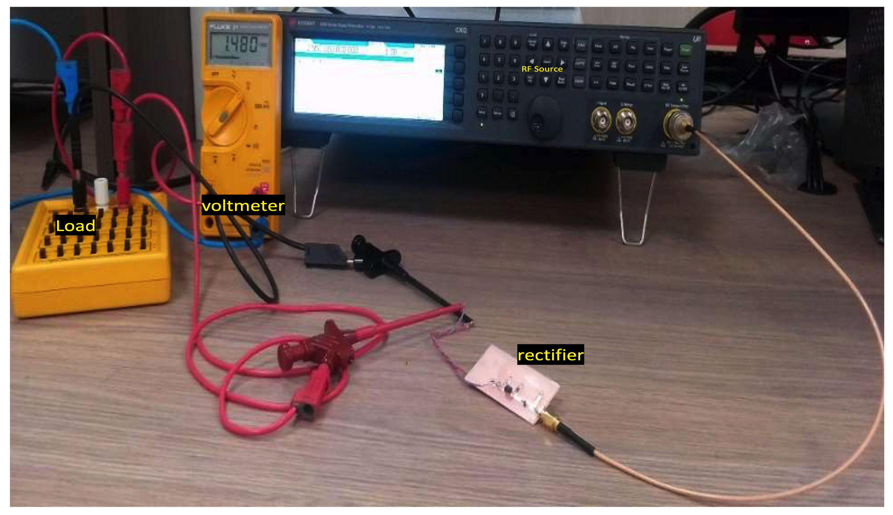
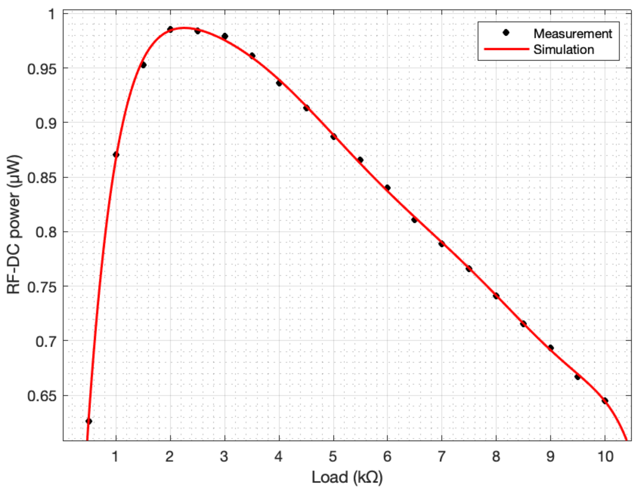
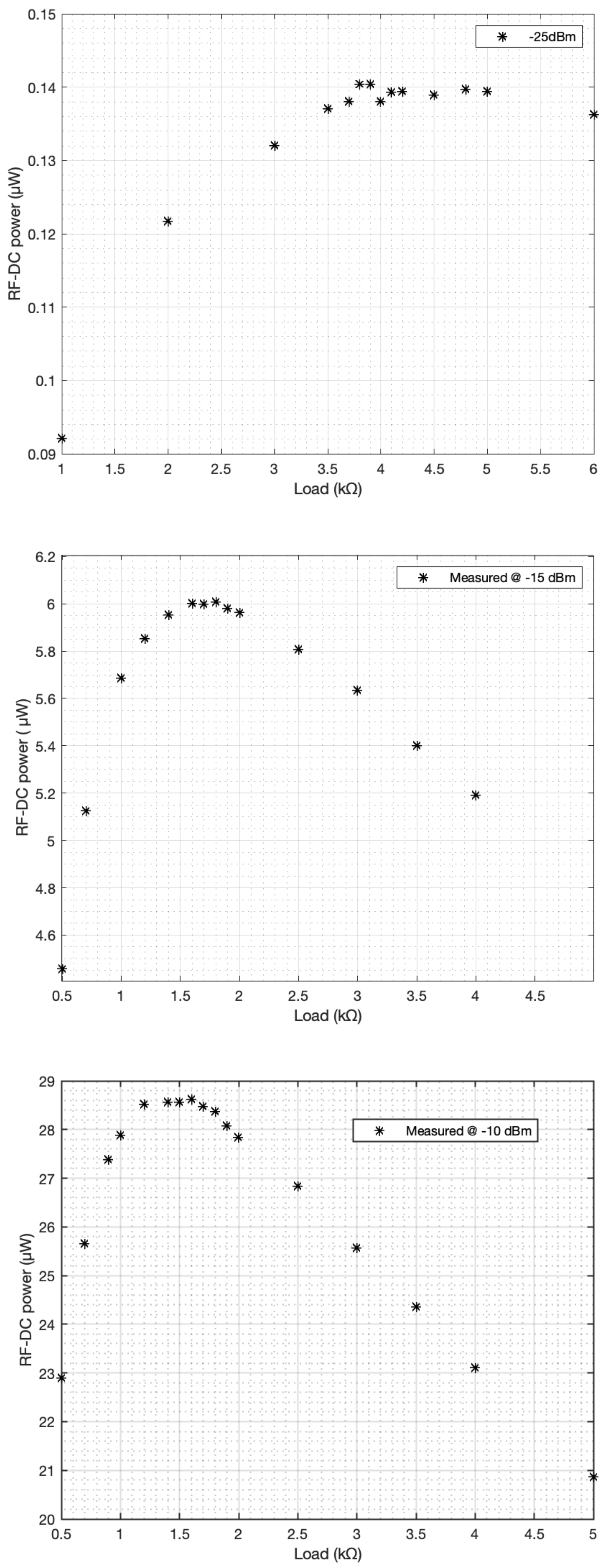
3.3. Measurement and Maximum Power Point
- The simulation layout is generated from the schematic design software. Pins’ effects are added as lump components at the various gaps between ground and input power supply (Figure 13).
- The frequency range is set between 2 GHz to 3 GHz in the momentum co-simulation.
- The lumped components, ground, power supply, via to ground and via to inductor are connected to the schematic in (Figure 10a).
- Parasitics: the existence of parasitic components in the diode may limit the PCE. The diode junction resistor, R, causes losses. At high frequency, the junction capacitance and package inductance also limit the PCE [39].
- Threshold and reverse-breakdown voltage: the diode threshold voltage requires the energy harvester to be supplied with sufficient input RF power. This limits the sensitivity of the RFEH circuit. The effect of diode breakdown voltage occurs when the diode DC bias voltage is half the breakdown voltage. This is why the power curves in Figure 15 and Figure 16 begin to decrease above this point.
- Harmonics at the output: the non-linearity of the diode creates harmonics in the output voltage, responsible for losses.
- Impedance matching: as the diode behavior changes with the input RF power, the input matching deviates and part of the incident energy is reflected to the surroundings. This reflected power causes a reduction in the amount of energy available for rectification. PCE is negatively impacted.
4. Conclusions

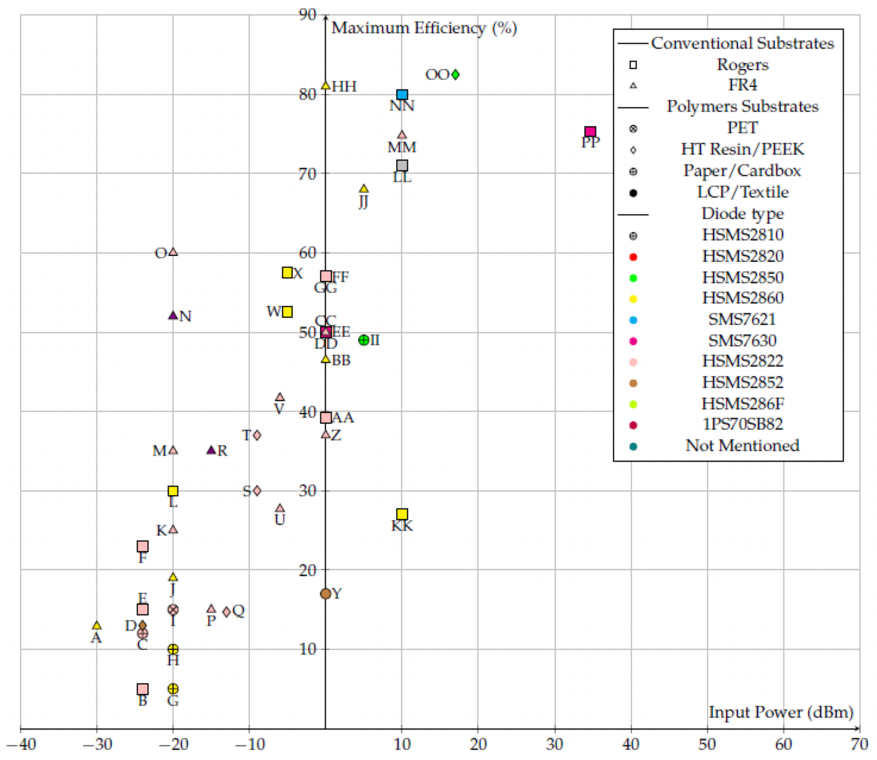
| Frequency (GHz) | Pin(dBm)@ Load (k) | PCE@RF-DC Power | Substrate/Printing Tech | Size (mm × mm × mm) | Ref |
|---|---|---|---|---|---|
| 2.45 | −24@10 | 13%@0.52 W | Resin/Stereolithography 3D printing polymer | 60 × 83 × 1.5 | [8] |
| 2.45 | −20@1 | 5%@0.5 W | LCP/Not mention | 15.1 × 8.15 × 0.18 | [25] |
| 2.45 | −20@1 | 5%@0.5 W | LCP/Not mention | 15.1 × 8.15 × 0.18 | [25] |
| 2.5 | −20@3 | 5%@0.5 W | Flexible paper/copper tape | 11 × 11 × 0.37 | [9] |
| 2.3 | −[email protected] | 5%@0.2 W | Duroid 5880/Conventional deposition (Rectifier)(PCB) | 32 × 32 × 1.575 | [7] |
| 2.4 | −[email protected] | 13%@1.3 W | FR4/printed circuit board | 32.07 × 35.75 × 1.6 | [13] |
| 0.915 | [email protected] | 55%@550 W | flexible printed circuit board (PCB) | Not Mentioned | [47] |
| 2.45 | −24.3@4 | 21%@0.78 W | Duroid 5880/ Conventional deposition (Rectifier)(PCB) | 105 × 87 × 3.7 | [48] |
| 2.45 | −[email protected] | 15%@1.5 W | Duroid 5880/ Conventional deposition (Rectifier)(PCB) | 32 × 32 × 1.575 | [7] |
| 2.1 | −24@11 | 3%@0.12 W | 3D printing substrate/Screen printing (conductive silver paste from DuPont) | 50 × 50 × 50 | [5] |
| 2.45 | −[email protected] | 19%@ 6 W | PLA/Fuse Deposition Modelling 3D printing polymer | 42 × 14 × 1.5 | This Work |
| −20@2 −[email protected] −[email protected] | 9.6%@0.96 W 4.43%@0.14 W 28.75%@ 28.75 |
Author Contributions
Funding
Acknowledgments
Conflicts of Interest
Abbreviations
| DC | Direct Current |
| RFEH | Radio Frequency Energy Harvesting |
| HBS | Harmonic Balance Simulation |
| LSSP | Large Signal Scattering Parameter |
| MPP | Maximum Power Point |
| PCE | Power Conversion Efficiency |
| PLA | Polylactic Acid polymer |
| TTL | Two Transmission Line |
References
- Newell, D. Optimised Energy Management for Energy Harvesting Powered Wireless Sensors; NUI Galway: Galway, Ireland, 2018. [Google Scholar]
- Sezer, N.; Koç, M. A comprehensive review on the state-of-the-art of piezoelectric energy harvesting. Nano Energy 2021, 80, 105567. [Google Scholar] [CrossRef]
- European Comission. Up to 78 Million Batteries Will Be Discarded Daily by 2025, Researchers Warn; European Comission: Brussels, Belgium, 2021.
- Georgiadis, A.; Collado, A.; Via, S.; Meneses, C. Flexible hybrid solar/EM energy harvester for autonomous sensors. In Proceedings of the MTT-S International Microwave Symposium Digest, Baltimore, MD, USA, 4–11 June 2011; pp. 6–9. [Google Scholar] [CrossRef]
- Bakytbekov, A.; Nguyen, T.Q.; Huynh, C.; Salama, K.N.; Shamim, A. Fully Printed 3D Cube-Shaped Multiband Fractal Rectenna for Ambient RF Energy Harvesting. Nano Energy 2018, 53, 587–595. [Google Scholar] [CrossRef]
- Muhammad, S.; Tiang, J.J.; Wong, S.K.; Smida, A.; Ghayoula, R.; Iqbal, A. A Dual-Band Ambient Energy Harvesting Rectenna Design for Wireless Power Communications. IEEE Access 2021, 9, 99944–99953. [Google Scholar] [CrossRef]
- Song, C.; Huang, Y.; Zhou, J.; Zhang, J.; Yuan, S.; Carter, P. A high-efficiency broadband rectenna for ambient wireless energy harvesting. IEEE Trans. Antennas Propag. 2015, 63, 3486–3495. [Google Scholar] [CrossRef]
- Linh Nguyen, X.V.; Gerges, T.; Duchamp, J.M.; Benech, P.; Verdier, J.; Lombard, P.; Cabrera, M.; Allard, B. Stereolithography-Based Rectenna for Wireless Energy Harvesting. In Proceedings of the 34th International System-on-Chip Conference (SOCC), Las Vegas, NV, USA, 14–17 September 2021; pp. 34–39. [Google Scholar] [CrossRef]
- Palazzi, V.; Hester, J.; Bito, J.; Alimenti, F.; Kalialakis, C.; Collado, A.; Mezzanotte, P.; Georgiadis, A.; Roselli, L.; Tentzeris, M.M. A Novel Ultra-Lightweight Multiband Rectenna on Paper for RF Energy Harvesting in the Next Generation LTE Bands. IEEE Trans. Microw. Theory Tech. 2018, 66, 366–379. [Google Scholar] [CrossRef]
- Awais, Q.; Jin, Y.; Chattha, H.T.; Jamil, M.; Qiang, H.; Khawaja, B.A. A Compact Rectenna System With High Conversion Efficiency for Wireless Energy Harvesting. IEEE Access 2018, 6, 35857–35866. [Google Scholar] [CrossRef]
- Roy, S.; Tiang, J.J.; Roslee, M.B.; Ahmed, M.T.; Kouzani, A.Z.; Mahmud, M.P. Quad-band rectenna for ambient radio frequency (RF) energy harvesting. Sensors 2021, 21, 7838. [Google Scholar] [CrossRef]
- Hucheng, S.; Guo, Y.-X.; He, M.; Zhong, Z. A dual-band rectenna using broadband yagi antenna array for ambient rf power harvesting. IEEE Antennas Wirel. Propag. Lett. 2013, 12, 918–921. [Google Scholar] [CrossRef]
- Roy, S.; Tiang, J.J.; Roslee, M.B.; Ahmed, M.T.; Kouzani, A.Z.; Mahmud, M.P. Design of a Highly Efficient Wideband Multi-Frequency Ambient RF Energy Harvester. Sensors 2022, 22, 424. [Google Scholar] [CrossRef]
- Hamidouche, A.M.; Takhedmit, H.; Poulichet, P.; Cirio, L. Efficiency improvement of an UWB rectifier by using optimized pulse modulation signal: Simulation and experiments. In Proceedings of the Wireless Power Week (WPW), Bordeaux, France, 5–8 July 2022; pp. 407–411. [Google Scholar] [CrossRef]
- Nguyen, X.V.L.; Gerges, T.; Duchamp, J.M.; Benech, P.; Verdier, J.; Lombard, P.; Cabrera, M.; Allard, B. 3D Plastronics Radio Frequency Energy Harvester on Stereolithography Parts. In Proceedings of the Wireless Power Week (WPW), Bordeaux, France, 5–8 July 2022; pp. 156–161. [Google Scholar] [CrossRef]
- Niotaki, K.; Kim, S.; Jeong, S.; Collado, A.; Georgiadis, A.; Tentzeris, M.M. A Compact Dual-Band Rectenna Using Slot-Loaded Dual Band Folded Dipole AntennaKyriaki. IEEE Antennas Wirel. Propag. Lett. 2013, 12, 1634–1637. [Google Scholar] [CrossRef]
- Khalid, F.; Saeed, W.; Shoaib, N.; Khan, M.U.; Cheema, H.M. Quad-Band 3D Rectenna Array for Ambient RF Energy Harvesting. Int. J. Antennas Propag. 2020, 2020, 7169846. [Google Scholar] [CrossRef]
- Shen, S.; Chiu, C.Y.; Murch, R.D. A dual-port triple-band L-probe microstrip patch rectenna for ambient RF energy harvesting. IEEE Antennas Wirel. Propag. Lett. 2017, 16, 3071–3074. [Google Scholar] [CrossRef]
- Lin, C.H.; Chiu, C.W.; Gong, J.Y. A Wearable Rectenna to Harvest Low-Power RF Energy for Wireless Healthcare Applications. In Proceedings of the 11th International Congress on Image and Signal Processing, BioMedical Engineering and Informatics (CISP-BMEI), Beijing, China, 13–15 October 2018; pp. 1–5. [Google Scholar] [CrossRef]
- Mansour, M.M.; Kanaya, H. Compact RF rectifier circuit for ambient energy harvesting. In Proceedings of the International Symposium on Radio-Frequency Integration Technology, RFIT 2017, Seoul, Republic of Korea, 30 August–1 September 2017; pp. 220–222. [Google Scholar] [CrossRef]
- Ur Rehman, M.; Ahmad, W.; Khan, W.T. Highly efficient dual band 2.45/5.85 GHz rectifier for RF energy harvesting applications in ISM band. In Proceedings of the Asia-Pacific Microwave Conference, Kuala Lumpur, Malaysia, 13–16 November 2017; pp. 150–153. [Google Scholar] [CrossRef]
- Tafekirt, H.; Pelegri-Sebastia, J.; Bouajaj, A.; Reda, B.M. A Sensitive Triple-Band Rectifier for Energy Harvesting Applications. IEEE Access 2020, 8, 73659–73664. [Google Scholar] [CrossRef]
- Almoneef, T.S. Design of a Rectenna Array without a Matching Network. IEEE Access 2020, 8, 109071–109079. [Google Scholar] [CrossRef]
- Eid, A.; Costantine, J.; Tawk, Y.; Ramadan, A.H.; Abdallah, M.; Elhajj, R.; Awad, R.; Kasbah, I.B. An efficient RF energy harvesting system. In Proceedings of the 11th European Conference on Antennas and Propagation, EUCAP 2017, Paris, France, 19–24 March 2017; pp. 896–899. [Google Scholar] [CrossRef]
- Eid, A.; Hester, J.G.; Costantine, J.; Tawk, Y.; Ramadan, A.H.; Tentzeris, M.M. A Compact Source-Load Agnostic Flexible Rectenna Topology for IoT Devices. IEEE Trans. Antennas Propag. 2020, 68, 2621–2629. [Google Scholar] [CrossRef]
- Papadopoulou, M.S.; Boursianis, A.D.; Volos, C.K.; Stouboulos, I.N.; Nikolaidis, S.; Goudos, S.K. High-Efficiency Triple-Band RF-to-DC Rectifier Primary Design for RF Energy-Harvesting Systems. Telecom 2021, 2, 271–284. [Google Scholar] [CrossRef]
- Khonsari, Z.; Björninen, T.; Tentzeris, M.M.; Sydänheimo, L.; Ukkonen, L. 2.4 GHz inkjet-printed RF energy harvester on bulk cardboard substrate. In Proceedings of the Radio and Wireless Symposium (RWS), San Diego, CA, USA, 25–28 January 2015; pp. 153–155. [Google Scholar] [CrossRef]
- Mouapi, A.; Hakem, N.; Kandil, N.; Kamani, G.V. A Miniature Rectifier Design for Radio Frequency Energy Harvesting Applied at 2.45 GHz. In Proceedings of the International Conference on Environment and Electrical Engineering and Industrial and Commercial Power Systems Europe, EEEIC/I and CPS Europe 2018, Palermo, Italy, 12–15 June 2018; pp. 1–5. [Google Scholar] [CrossRef]
- Asakura, S.; Yamanokuchi, S.; Yoshida, S.; Nishikawa, K. Design and Prototyping of a Single-Shunt Rectifier with 71% Fractional Bandwidth Having Acceptable Matching on 10 dBm LSSP. In Proceedings of the Wireless Power Week (WPW), Bordeaux, France, 5–8 July 2022; pp. 383–387. [Google Scholar] [CrossRef]
- Hoque, M.U.; Kumar, D.; Audet, Y.; Savaria, Y. Design and Analysis of a 35 GHz Rectenna System for Wireless Power Transfer to an Unmanned Air Vehicle. Energies 2022, 15, 320. [Google Scholar] [CrossRef]
- Kawai, K.; Takabayashi, N.; Toyonaga, T.; Suzuki, K.; Shinohara, N. Development of Rectenna for Estimating Received Power Level Using Second Harmonic Wave. In Proceedings of the Wireless Power Week (WPW), Bordeaux, France, 5–8 July 2022; pp. 175–179. [Google Scholar] [CrossRef]
- Ferrari, P.; Flechet, B.; Angenieux, G. Time domain characterization of lossy arbitrary characteristic impedance transmission lines. IEEE Microw. Guid. Wave Lett. 1994, 4, 177–179. [Google Scholar] [CrossRef]
- Mpele, M.P.; Mbango, F.M.; Konditi, D.B.O.; Ndagijimana, F. A novel quadband ultra miniaturized planar antenna with metallic vias and defected ground structure for portable devices. Heliyon 2021, 7, e06373. [Google Scholar] [CrossRef]
- Din, N.M.; Chakrabarty, C.K.; Bin Ismail, A.; Devi, K.K.; Chen, W.Y. Design of RF energy harvesting system for energizing low power devices. Prog. Electromagn. Res. 2012, 132, 49–69. [Google Scholar] [CrossRef]
- Majumder, A. Rectangular Microstrip Patch Antenna Using Coaxial Probe Feeding Technique to Operate in S-Band. Int. J. Eng. Trends Technol. 2013, 4, 1206–1210. [Google Scholar]
- Thakur, A.; Chauhan, M.; Kumar, M. Effect of substrate relative dielectric constant on bandwidth characteristics of line feed rectangular patch antenna. Int. J. Eng. Sci. Invent. Res. Dev. 2015, 1. Available online: https://portal.issn.org/resource/ISSN/2349-6185 (accessed on 30 March 2023).
- Zhou, Y. Contribution to Electromagnetic Energy Harvesting for Wireless Autonomous Devices. Ph.D. Thesis, Université de Nantes, Nantes, France, 2015. [Google Scholar]
- Marc, E.; Goldfarb, R.A.P. Modeling Via Hole Grounds in Microstrip. IEEE Microw. Guid. Wave Lett. 1991, 1, 135–137. [Google Scholar] [CrossRef]
- Valenta, C.R.; Durgin, G.D. Harvesting wireless power: Survey of energy-harvester conversion efficiency in far-field, wireless power transfer systems. IEEE Microw. Mag. 2014, 15, 108–120. [Google Scholar] [CrossRef]
- Munir, A.; Asthan, R.S.; Prananto, H.D.; Oktafiani, F. Design and characterization of PLA-based wideband 3D-printed discone antenna. In Proceedings of the International Symposium on Antennas and Propagation and USNC-URSI Radio Science Meeting (AP-S/URSI), Denver, CO, USA, 10–15 July 2022; pp. 593–594. [Google Scholar]
- Silva, J.S.; Garcia-Vigueras, M.; Debogović, T.; Costa, J.R.; Fernandes, C.A.; Mosig, J.R. Stereolithography-based antennas for satellite communications in Ka-band. Proc. IEEE 2017, 105, 655–667. [Google Scholar] [CrossRef]
- Kimionis, J.; Georgiadis, A.; Isakov, M.; QI, H.; Tentzeris, M. 3D/inkjet-printed origami antennas for multi-direction RF harvesting. In Proceedings of the MTT-S International Microwave Symposium, Phoenix, AZ, USA, 17–22 May 2015. [Google Scholar]
- Wahyudi, A.H.; Sumantyo, J.T.S.; Wijaya, S.; Munir, A. PLA-based 3D printed circularly polarized X-band horn array antenna for CP-SAR sensor. In Proceedings of the International Workshop on Antenna Technology (iWAT), Nanjing, China, 5–7 March 2018; pp. 1–4. [Google Scholar]
- Piekarz, I.; Sorocki, J.; Slomian, I.; Wincza, K.; Gruszczynski, S. Experimental verification of 3D printed low-conductivity graphene-enhanced PLA absorbers for back lobe suppression in aperture-coupled antennas. In Proceedings of the IEEE-APS Topical Conference on Antennas and Propagation in Wireless Communications (APWC), Cartagena, Colombia, 10–14 September 2018; pp. 780–782. [Google Scholar]
- Oktafiani, F.; Hamid, E.Y.; Munir, A. Characterization of PLA-based Quad-Ridged Horn Antenna. In Proceedings of the Region 10 Conference (TENCON), Osaka, Japan, 16–19 November 2020; pp. 897–900. [Google Scholar]
- Munir, A.; Asthan, R.S.; Oktafiani, F. 3D Printing Technology for Rapid Manufacturing Discone Antenna Based on PLA Material. In Proceedings of the 14th International Conference on Computational Intelligence and Communication Networks (CICN), Al-Khobar, Saudi Arabia, 4–6 December 2022; pp. 637–640. [Google Scholar]
- Wagih, M.; Weddell, A.S.; Beeby, S. Powering E-Textiles Using a Single Thread Radio Frequency Energy Harvesting Rectenna. Proceedings 2021, 68, 16. [Google Scholar]
- Adami, S.E.; Proynov, P.; Hilton, G.S.; Yang, G.; Zhang, C.; Zhu, D.; Li, Y.; Beeby, S.P.; Craddock, I.J.; Stark, B.H. A flexible 2.45-GHz power harvesting wristband with net system output from- 24.3 dBm of RF power. IEEE Trans. Microw. Theory Tech. 2017, 66, 380–395. [Google Scholar] [CrossRef]


| Frequency (GHz) | tan | L1/L2(mm) | Method | Ref | |
|---|---|---|---|---|---|
| 0.02–3 | 0.0004–0.04 | 2–4 | 80/100 | TTL | [8] |
| 0.5–5 | 0.015–0.024 | 2.52–2.91 | 10/20 | TTL | [25] |
| 2.4–5.4 | 0.02–0.04 | 2.8–3.2 | 19/30 | TTL | [9] |
| 2.4–5.4 | 0.003–0.04 | 2.05–3.15 | 19/24 | Not Given | [7] |
| 0.5–3 | Not Given | 1.8–2.7 | 10/20 | TTL | [21] |
| 2.2–2.8 | 0.001–0.09 | 2.7–2.9 | 40/70 | TL | This Work |
| Wp | Lp | Wf | Lf | Wx | Wc | Ws | Ls | Li |
|---|---|---|---|---|---|---|---|---|
| 54 | 35.9 | 3.4 | 26.5 | 24.5 | 0.8 | 80 | 70 | 9.5 |
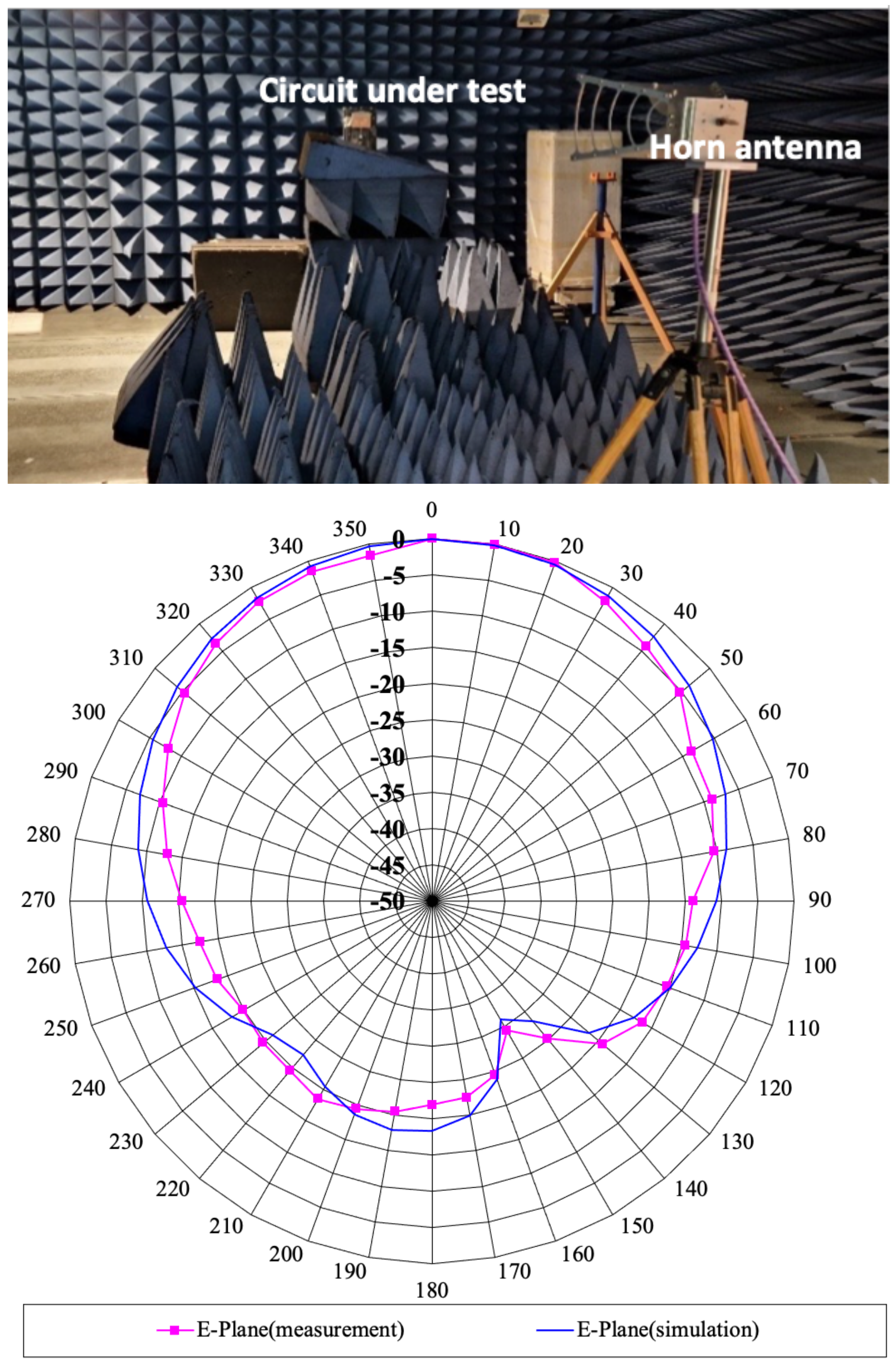
| Material | Gain (dB) | Bandwidth (MHz) | Resonance Frequency (GHz) | S11 (dB) | Size (mm × mm × mm) |
|---|---|---|---|---|---|
| PLA Simulation | 8 | 58 | 2.453 | −24.48 | 70 × 80 × 1.5 |
| PLA Measurement | 7.94 | 60 | 2.446 | −18.45 | 70 × 80 × 1.5 |
| Rogers Simulation | 8.4 | 46.4 | 2.45 | −25.16 | 58 × 70 × 1.5 |
| Rogers Measurement | 8.02 | 46.2 | 2.452 | −21.15 | 58 × 70 × 1.5 |
Disclaimer/Publisher’s Note: The statements, opinions and data contained in all publications are solely those of the individual author(s) and contributor(s) and not of MDPI and/or the editor(s). MDPI and/or the editor(s) disclaim responsibility for any injury to people or property resulting from any ideas, methods, instructions or products referred to in the content. |
© 2023 by the authors. Licensee MDPI, Basel, Switzerland. This article is an open access article distributed under the terms and conditions of the Creative Commons Attribution (CC BY) license (https://creativecommons.org/licenses/by/4.0/).
Share and Cite
Linge, P.U.; Gerges, T.; Bevilacqua, P.; Duchamp, J.-M.; Benech, P.; Verdier, J.; Lombard, P.; Cabrera, M.; Tsafack, P.; Mieyeville, F.; et al. Evaluation of Polylactic Acid Polymer as a Substrate in Rectenna for Ambient Radiofrequency Energy Harvesting. J. Low Power Electron. Appl. 2023, 13, 34. https://doi.org/10.3390/jlpea13020034
Linge PU, Gerges T, Bevilacqua P, Duchamp J-M, Benech P, Verdier J, Lombard P, Cabrera M, Tsafack P, Mieyeville F, et al. Evaluation of Polylactic Acid Polymer as a Substrate in Rectenna for Ambient Radiofrequency Energy Harvesting. Journal of Low Power Electronics and Applications. 2023; 13(2):34. https://doi.org/10.3390/jlpea13020034
Chicago/Turabian StyleLinge, Pangsui Usifu, Tony Gerges, Pascal Bevilacqua, Jean-Marc Duchamp, Philippe Benech, Jacques Verdier, Philippe Lombard, Michel Cabrera, Pierre Tsafack, Fabien Mieyeville, and et al. 2023. "Evaluation of Polylactic Acid Polymer as a Substrate in Rectenna for Ambient Radiofrequency Energy Harvesting" Journal of Low Power Electronics and Applications 13, no. 2: 34. https://doi.org/10.3390/jlpea13020034