Article

Simple Technique to Improve Essentially the Performance of One-Stage Op-Amps in Deep Submicrometer CMOS Technologies

by
Jaime Ramirez-Angulo
1,*,
Alejandra Diaz-Armendariz
2,
Jesus E. Molinar-Solis
3,
Alejandro Diaz-Sanchez
4 and
Jesus Huerta-Chua
1
1
Electronics Dept., Instituto Tecnologico Superior de Poza Rica, Poza Rica 93239, Mexico
2
Intel Guadalajara, Zapopan 45017, Mexico
3
Electronics Dept., Tecnologico Nacional de Mexico/ITCG, Cd Guzman 49100, Mexico
4
Electronics Dept., Instituto Nacional de Astrofisica, Optica y Electronica, Tonantzintla 72840, Mexico
*
Author to whom correspondence should be addressed.
J. Low Power Electron. Appl. 2023, 13(1), 4; https://doi.org/10.3390/jlpea13010004
Submission received: 5 October 2022 / Revised: 27 December 2022 / Accepted: 29 December 2022 / Published: 4 January 2023

Abstract

:
A comparative study of one-stage-amp performance improvement based on simulations in 22 nm, 45 nm, 90 nm, and 180 nm in deep submicrometer CMOS technologies is discussed. Generic SPICE models were used to simulate the circuits. It is shown that in all cases a simple modification using resistive local common mode feedback increases open-loop gain and gain-bandwidth product, peak output currents, and slew rate by close to an order of magnitude. It is shown that this modification is especially appropriate for its utilization in current CMOS technologies since large factor improvements were not available in previous technologies. The OTAs with resistive local common mode feedback require simple phase lead compensation with a very small additional silicon area and keep supply requirements and static power dissipation unchanged.

1. Introduction

Deep submicrometer CMOS technologies use sub-volt supply voltages that do not allow the use of cascode transistors in the output branch of op-amps. This is due to the fact that as feature sizes have decreased threshold voltages have not scaled down at the same rate as the supplies and they are a significant fraction of the supply voltages in current CMOS technologies. For this reason, cascode transistors in the output branches would seriously limit the output signal swing and are avoided. The lack of cascode transistors leads to low open-loop gains Aol in one-stage op-amps (also denoted OTAs) on the order of Aol = gmro/2 = A/2, where gm is the small signal transconductance gain, ro the output resistance and A = gmro the intrinsic gain of a MOS transistor in a given technology. The resulting open-loop gain of a non-cascoded gate-driven one-stage op-amp (Figure 1a) is only typically around 25–30 dB. This results in op-amps with very poor accuracy since the open-loop gain of an op-amp determines its accuracy for closed loop applications. Two-stage Miller op-amps can be used to overcome the problem and to achieve a higher open-loop gain Aol = [(gmro)2]/2 (approximately 50–60 dB) but they require an area-intensive Miller compensation capacitance Cc whose value is typically similar to the load capacitance Cc = CL. Nested Miller compensated multistage op-amps can achieve higher open-loop gains but require complex compensation schemes which limit seriously their gain-bandwidth product or GB [1] and also require several silicon area-intensive capacitances. Assuming a typical design with Cc = CL, both, one- and two-stage op-amps are characterized by a gain-bandwidth product given by the same expression GB = (1/2π)(gm/CL) [2]. In [3], a very simple scheme using resistive local common mode feedback (RLCMFB) was used to increase Aol and GB of a non-cascoded one-stage op-amp and at the same time to provide efficient class AB operation. At the time the RLCMFB technique was introduced, only modest improvement could be achieved due to the relatively large feature sizes that MOS transistors had in those technologies. In this paper, we show that the RLCMFB technique allows essential OTA improvement in current submicrometer CMOS technologies. Section 2 of the paper discusses the basic aspects of the RLCMFB technique. Section 3 shows simulations of conventional and OTAS with RLCMFB in four submicromenter CMOS technologies. These simulations verify essential improvements in all figures of merit of non-cascoded OTAs with RLCMFB. Section 4 shows two comparison tables; one summarizing the simulation results of Section 3 and the second one comparing the OTA with RLCMFB to several recently published OTAs. Section 5 provides conclusions.

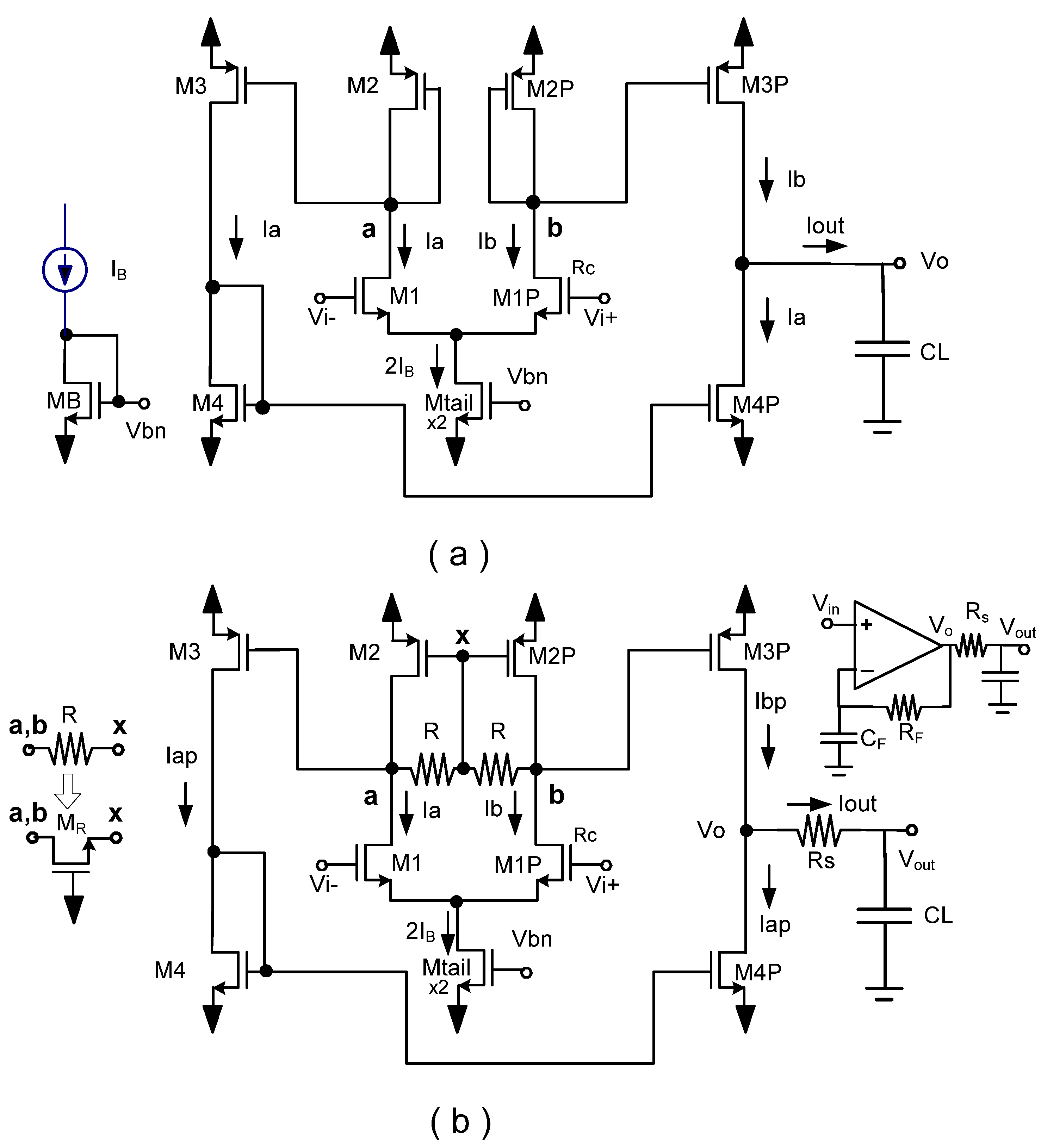
2. OTAs with Resistive Local Common Mode Feedback

The resistive local common mode feedback (RLCMF) technique uses resistors R in the input stage load (Figure 1b). It requires phase lead compensation to mitigate the effect on the OTA phase margin of the phase shift associated with high-frequency poles at nodes a,b introduced by the resistive local common mode feedback elements. Phase lead compensation uses just a resistor Rs in series with the output terminal to generate a zero with value ωz = 1/(RsCL) that approximately cancels the phase shift of poles at nodes a,b. These poles have values ωpa,b = 1/(RCPARa,b) where CPARa,b is the parasitic capacitance at nodes a,b. In this case, the op-amp performs approximately as a one-pole system with a (dominant) pole at the output node ωpout = 1/(RoutCL) = 1/((ro/2)CL). Resistive local common mode feedback with phase lead compensation leads to an open-loop gain enhanced by the factor Kenh = gm(R||ro1||ro2) according to: Aol = Kenhgmro/2 and also to an enhanced gain bandwidth product GB = Aolωpout = (1/2π)[Kenhgm/CL]. This is a factor Kenh higher than for conventional one- and two-stage op-amps. The resistive (and capacitive) local common mode feedback technique has been used extensively [4,5,6,7,8,9] to improve the performance of analog circuits, e.g., in the design of super class AB op-amps [5]. In previous CMOS technologies, the improvement factor Kenh of Aol and GB was limited to a relatively low value (few dB) due to the large minimum transistor feature sizes that introduced relatively large parasitic capacitances CPARa,b at nodes a and b. The large R required to achieve high Kenh values would lead to relatively low pole frequencies ωpa,b < GB that were difficult to cancel using phase lead compensation. In this paper, we show that the approach published in [3] is especially appropriate to enhance by relatively large factors Kenh (>10) the open-loop gain Aol, the gain-bandwidth product GB and the slew-rate SR of op-amps in modern deep submicrometer CMOS technologies. The reason being that with the reduction in feature sizes, parasitic capacitances CPARa,b at nodes a and b have very small values in current CMOS technologies, and even with relatively large R values, (comparable to ro) that lead to large Kenh factors, the poles ωpa,b at nodes a, b remain at relatively high. In this case, their phase shift (that decreases the phase margin) can be easily compensated with a phase lead compensation resistors Rs. This resistor is on chip and introduces a high frequency zero at ωz = 1/(RsCL) whose phase shift improves the phase margin of the OTA as discussed in [3]. No accurate matching of ωz and ωpab is required to achieve sufficient OTA phase margin. Given that ωz and ωpab are both at frequencies higher than GB (factor 1 to 3) the pole-zero doublet does not cause long settling times as explained in [10].
Figure 1. (a) Conventional one-stage op-amp without cascoding transistors. (b) One-stage op-amp with resistive local common mode feedback.
Jlpea 13 00004 g001

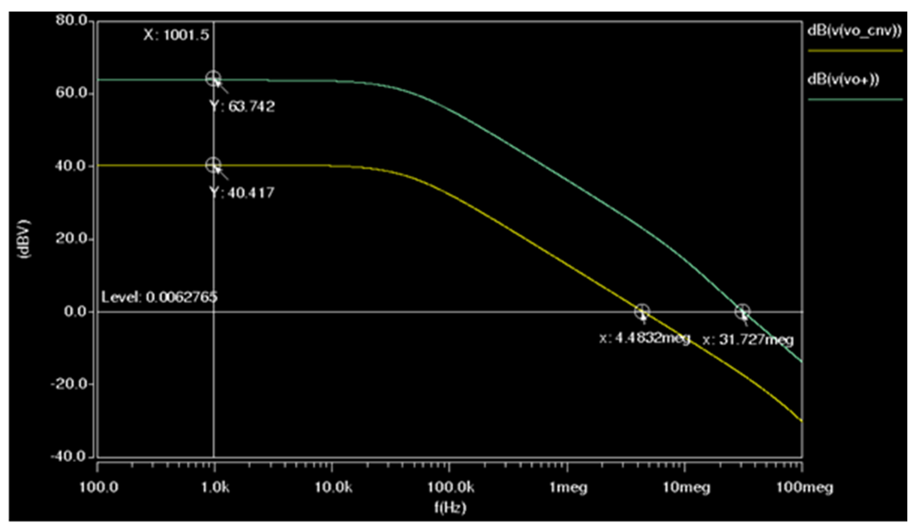
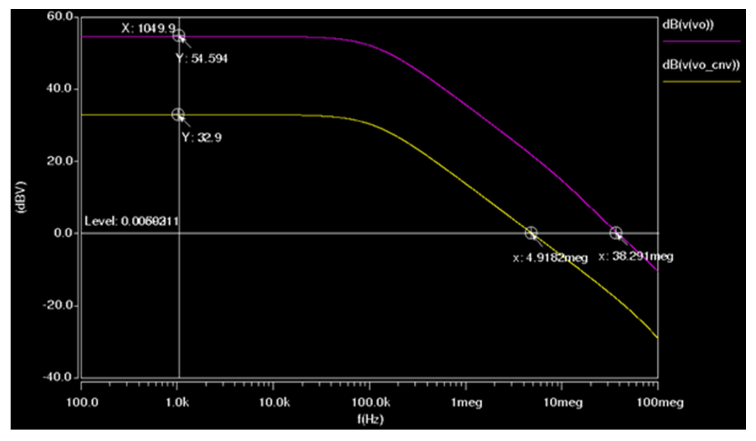
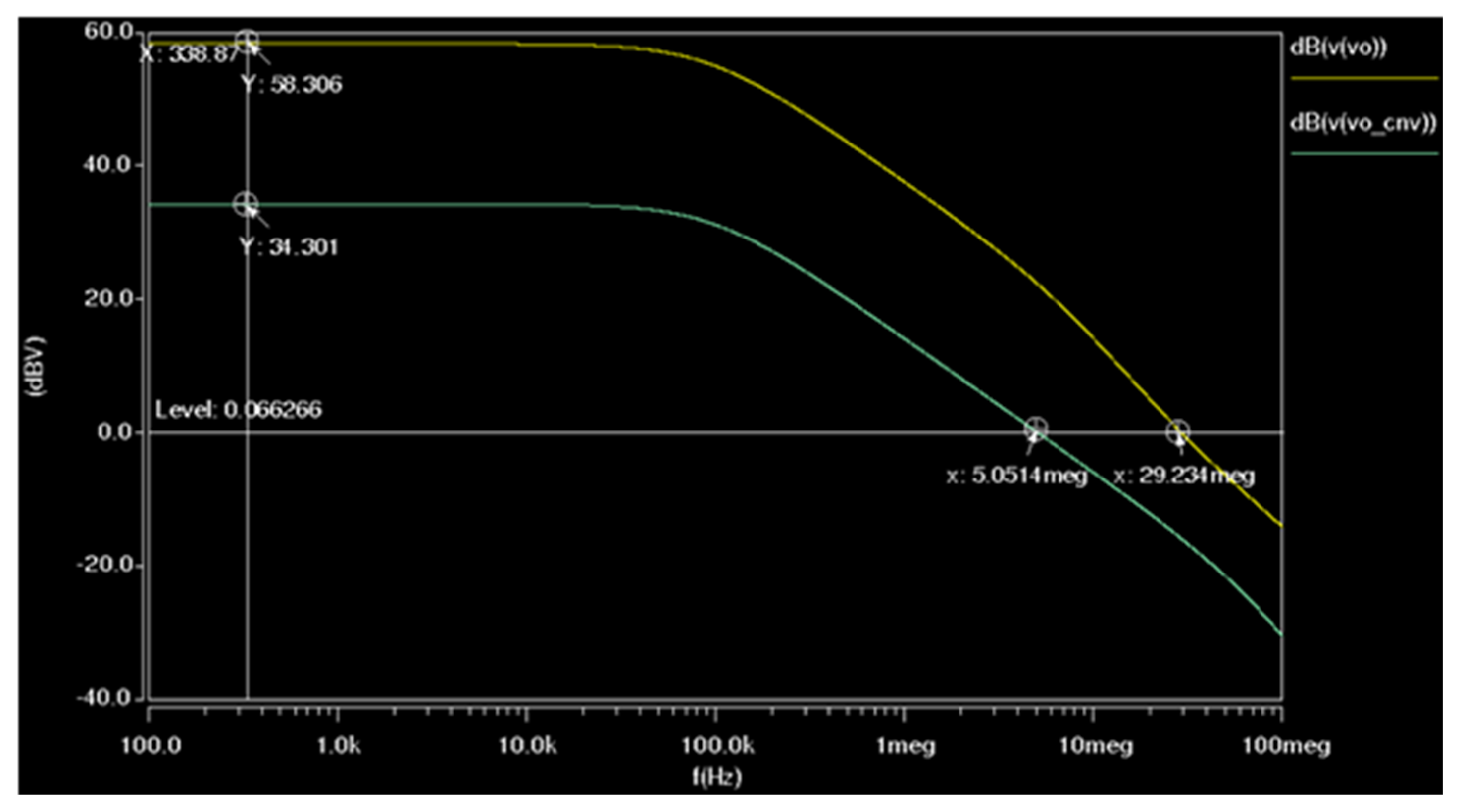
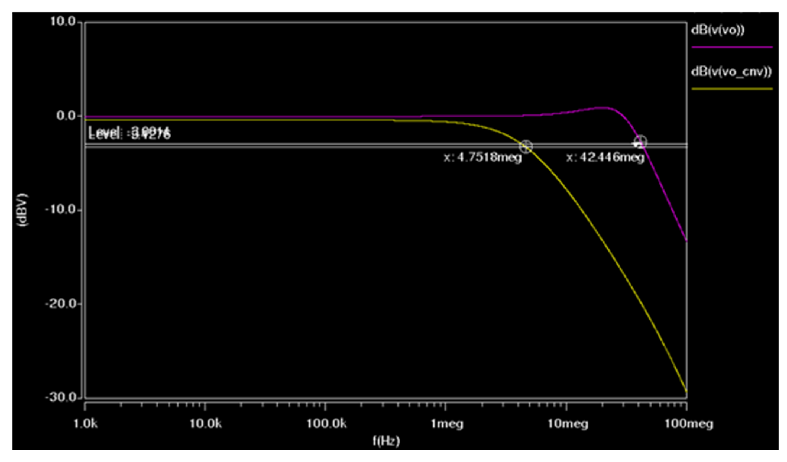
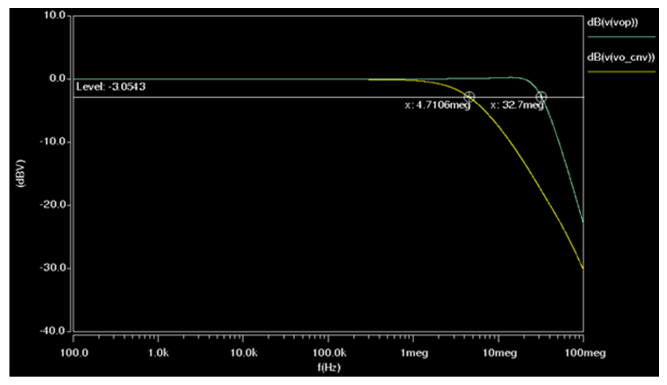
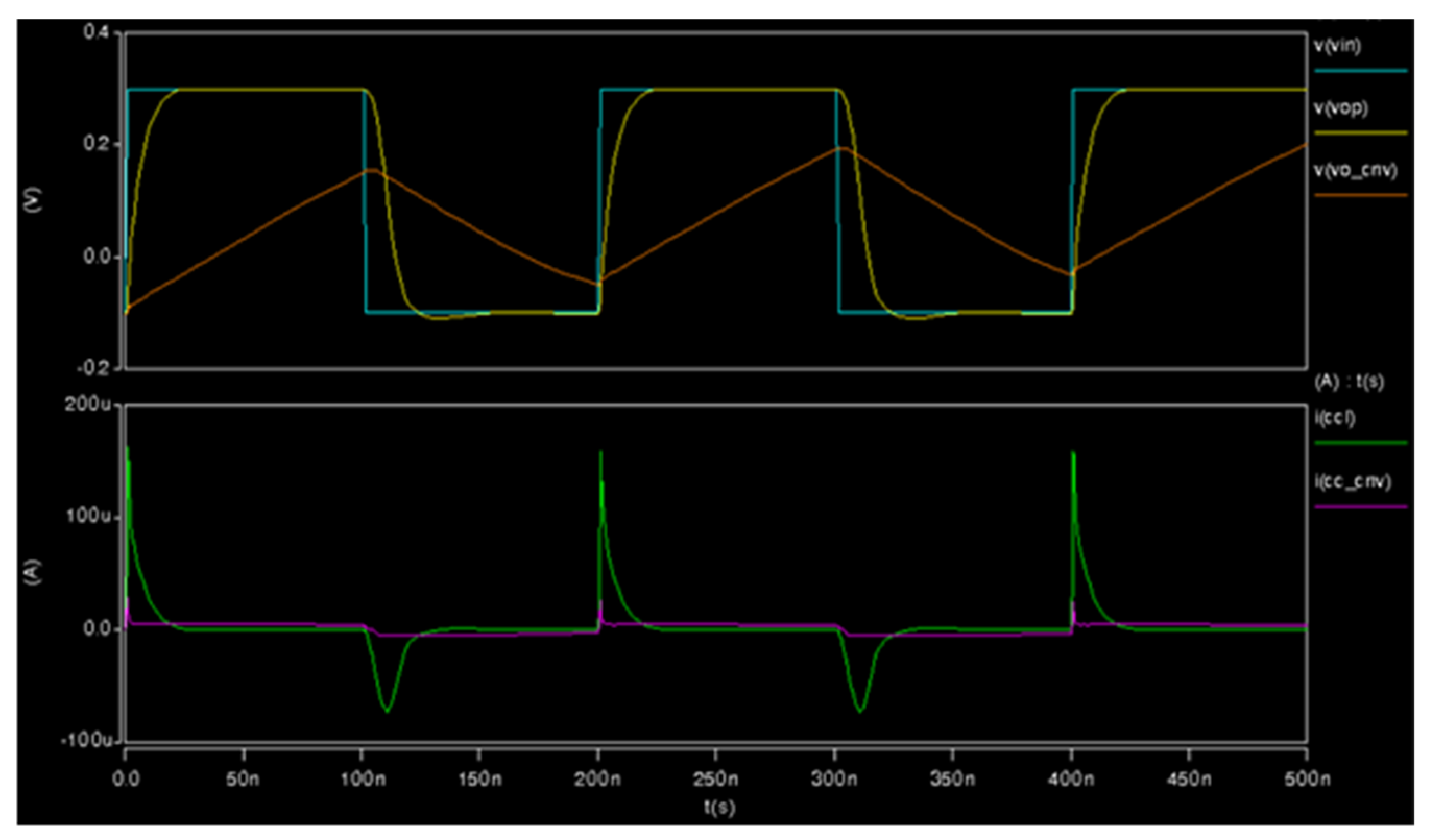
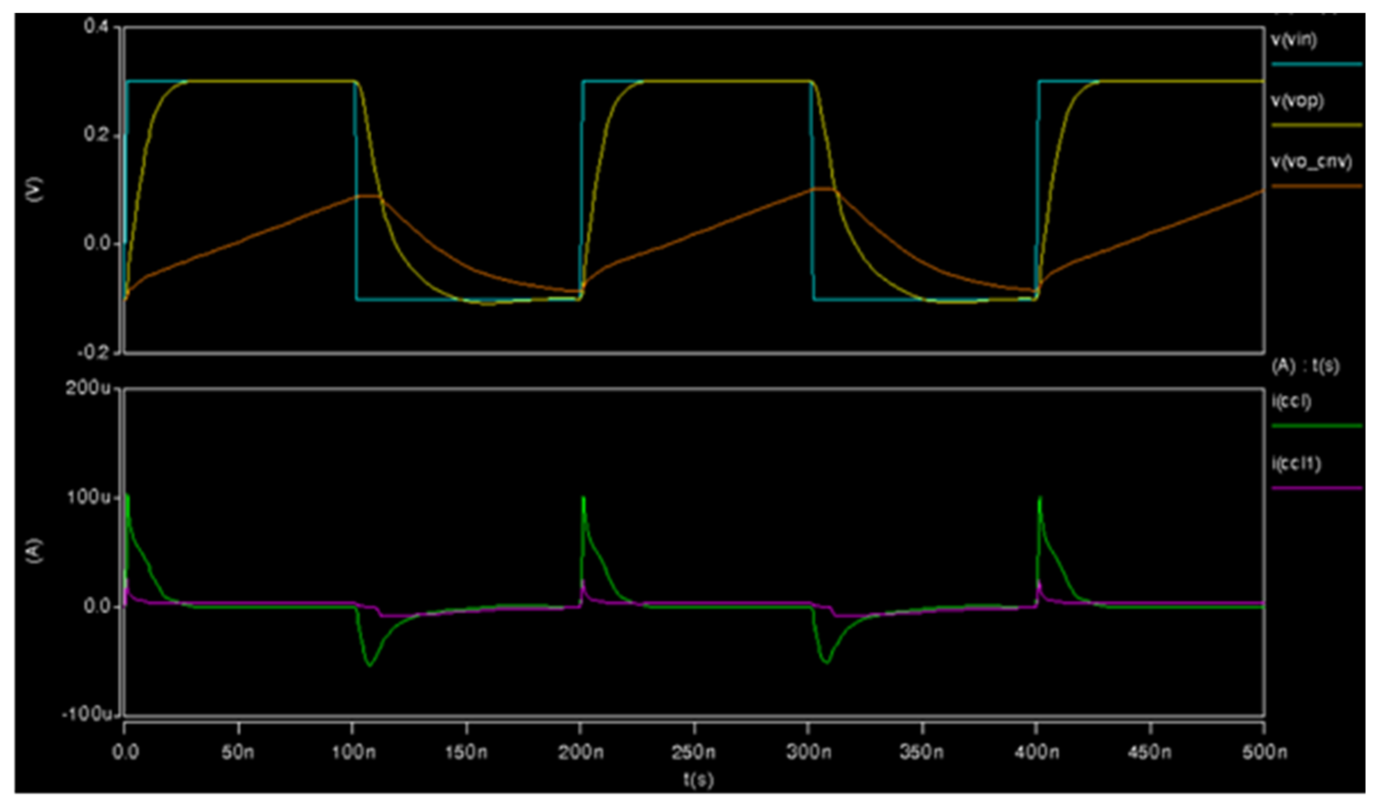
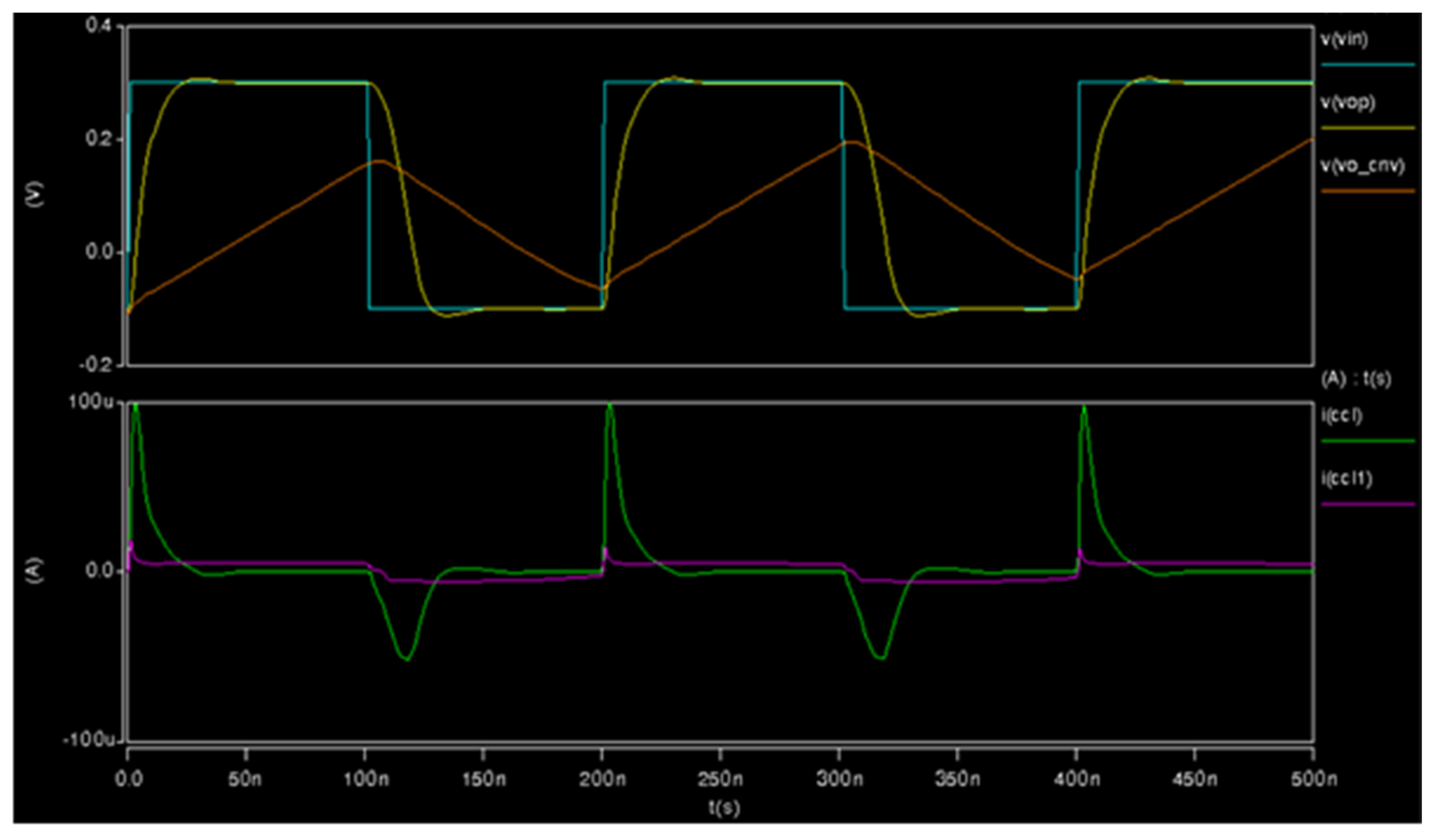
3. Simulation Results

A comparison among several simulations was made using 22 nm, 45 nm, 90 nm, and 180 nm CMOS technologies. The simulations in 22 nm, 45 nm, and 90 nm were performed with generic models available from North Carolina State University [11]. The simulations in 180 nm were performed using parameters of a TSMC commercial technology available through MOSIS [12]. In all cases, the bias current per branch is IB = 2.5 μA; therefore, the total quiescent current per circuit is ItotQ = 10 μA. For all circuits, PMOS and NMOS transistors had dimensions W = 10 µm and L = 2Lmin, where Lmin is the minimum feature size of the technology, also in all cases, the load capacitance was CL = 2pF. The simulated open-loop AC responses are depicted in Figure 2 for 22 nm. In this case, a value R = 500 kΩ was used. The trace v(vo_cnv) refers to the conventional topology of Figure 1a and v(vo) to the enhanced topology with resistive local common mode feedback of Figure 1b. Transistors operate in subthreshold and since they have the same bias currents their transconductance gains are similar. Values of resistors R were selected to obtain similar enhancement factors Kenh in all cases. The values of resistors R are not equal in all technologies since the output conductance of the transistors (which also affects Kenh as discussed in Section 2) are different in each technology. Simulations of the open-loop gain were performed by connecting a large valued feedback element RF (100 MΩ) from the output of the op-amp Vo (at the junction of the drains of M3P, M4P, and Rs) to the negative input as shown in Figure 1b. A grounded large valued grounded capacitance (CF = 1F) was connected to the OTA negative input terminal. The open-loop response displayed corresponds to the magnitude and phase of the voltage at the node labeled Vo in Figure 1.
AC simulations of the op-amp open-loop response for 45 nm, 90 nm, and 180 nm are shown in Figure 3, Figure 4 and Figure 5, respectively. The open-loop gain test setup using a very large resistive element RF = 100 MΩ and capacitor CF = 1F is shown in Figure 1b. Values R = 300 kΩ were used for 45 nm and 90 nm CMOS technologies. Values R = 500 kΩ were used for 180 nm CMOS technologies. In all cases, as it is common practice to save silicon area, resistors were implemented with transistors MR in triode mode as shown in Figure 1b. All of them with noticeable enhancements in Aol and GB for the op-amps with resistive local common mode feedback.
AC simulation results of the op-amps in voltage follower configuration (by connecting directly the output labeled Vo in Figure 1b to the negative op-amp input), are depicted in the same technologies, in Figure 6, Figure 7, Figure 8 and Figure 9. In all cases, the AC response of the voltage at the terminal labeled Vout in the circuits of Figure 1b and Vo in Figure 1a (at the ungrounded terminal of CL) is displayed. As can be noticed, the voltage follower bandwidth is improved by 5 to 10 times w.r.t those without resistive local common mode feedback.
The slew rate (SR) and the peak output current capability were determined by performing transient simulations applying a 5 MHz, 0.4VPP pulse input signal to the op-amps configured as voltage followers. Input and output voltage waveforms (top) as well as the load capacitor currents (bottom) for 22 nm, 45 nm, 90 nm, and 180 nm technologies are depicted in Figure 10, Figure 11, Figure 12 and Figure 13.
It can be seen that in all cases the conventional topology cannot follow the input signal adequately due to SR limitations, the enhanced topology with resistive local common mode feedback brings essentially higher peak output current capability (much higher than the bias current IB) while the conventional op-amps have positive and negative peak output currents limited by the bias current to a value IoutPK = 2IB = 5 µA.

4. Discussion

Table 1 summarizes the performance of the non-cascoded one-stage OTAs with RLCMFB and of the conventional non-cascoded one-stage OTAs (denoted CNV in the table). GB denotes the Gain-Bandwidth product, FOMSS = GB·CL/Pdis (in MHz·pF/μW units) is the small signal figure of merit where Pdis = ItotQVsupply denotes static power dissipation (ItotQ is the total quiescent current of the OTA), FOMLS = SR·CL/Pdis (in (V/μs)pF/μW units) is the large signal figure of merit and FOMGLB = (FOMS·FOML)1/2 is the global figure of merit. The slew rate (SR) used for the calculation of FOMLS is the minimum slew rate SR = min{SR+, SR−} (some authors use the average slew rate to calculate FOMLS instead of the minimum and report higher FOMLS but in practice, the minimum of the two slew rates is what limits the large signal speed of the OTA). The branch bias current IB of all circuits is IB = 2.5 µA, the total bias current of all circuits is ItotQ = 10 µA the power dissipation is Pdis = ItotQ(VDD−VSS), and has values Pdis = 4 µW for 22 nm, 4.5 µW for 45 nm and 90 nm and Pdis = 9 µW for 180 nm. The following facts are noticeable in Table 1:
(A)
The figures of merit in all technologies are a factor higher than 10 in OTAs with RLCMFB.
(B)
All figures of merit of OTAs with resistive local common mode feedback increase as the feature size of a CMOS technology decrease. One of the reasons is that supply voltages and static power dissipation also decrease with decreasing feature sizes and the standard figures of merit are inversely proportional to static power dissipation.
(C)
The main objective of this paper was to show that, even with relatively low CL values, it is possible to achieve significant performance enhancement factors (~1000%) using RLCMFB in current CMOS technologies. It might be possible to achieve even larger performance improvement factors by optimizing the OTA design (W/L values, R, Ibias, Rs) for each technology.
Table 2 shows a comparison of the performance of the OTAs with RLCMFB to OTAs published recently in the literature [13,14,15,16,17,18]. It can be seen that even without optimizing the designs, in all cases the FOMs of the RLCMFB OTAs are much higher than those in [13,14,15,16,17,18].

5. Conclusions

A comparative study of the performance of non-cascoded one-stage OTAs demonstrated that the inclusion of resistive common mode feedback is especially appropriate to increase significantly the OTA performance in current CMOS technologies. It is a very simple technique that improves Aol, GB, and SR and figures of merit by factors greater than 10 (or >1000%) without additional power dissipation or increased supply requirement and with very small additional silicon area and circuit complexity.

Author Contributions

Conceptualization, J.R.-A., A.D.-A., J.E.M.-S., A.D.-S. and J.H.-C.; Methodology, J.R.-A., A.D.-A., J.E.M.-S., A.D.-S. and J.H.-C.; Validation, J.R.-A., A.D.-A., J.E.M.-S., A.D.-S. and J.H.-C.; Formal Analysis, J.R.-A., A.D.-A., J.E.M.-S., A.D.-S. and J.H.-C.; writing—original draft preparation, J.R.-A. and J.E.M.-S.; writing—review and editing, J.R.-A. and J.E.M.-S.; visualization, J.R.-A. and J.E.M.-S.; supervision, J.R.-A. and J.E.M.-S.; project administration, J.R.-A. and J.E.M.-S.; funding acquisition, A.D.-S. All authors have read and agreed to the published version of the manuscript.

Funding

This work was supported in part by the Mexican Consejo Nacional de Ciencia y Tecnologia (CONACYT) by grant number A1-S-43214.

Data Availability Statement

Not applicable.

Conflicts of Interest

The authors declare no conflict of interest.

References

  1. Canizzaro, S.O.; Grasso, A.D.; Mita, R.; Palumbo, G. Design procedures for three-stage CMOS OTAs with nested-Miller compensation. IEEE Trans. Circuits Syst. I Regul. Pap. 2007, 54, 933–940. [Google Scholar] [CrossRef]
  2. Razavi, B. Operational Amplifiers. In Design of Analog CMOS Integrated Circuits, 1st ed.; McGraw-Hill: New York, NY, USA, 2001; pp. 291–324. [Google Scholar]
  3. Ramirez-Angulo, J.; Holmes, M. Simple technique using Local CMFB to enhance Slew Rate and bandwidth of one-Stage CMOS op-amps. Electron. Lett. 2002, 38, 1409–1411. [Google Scholar] [CrossRef]
  4. Harrison, J.; Weste, N. A 500 MHz CMOS anti-alias filter using feed-forward op-amps with local common-mode feedback. In Proceedings of the IEEE International Solid-State Circuits Conference, San Francisco, CA, USA, 13 February 2003. [Google Scholar]
  5. Baswa, S.; Ramirez-Angulo, J.; Lopez-Martin, A.J.; Carvajal, R.G.; Bikumandla, M. Rail-to-Rail super Class AB CMOS Operational Amplifiers. Electron. Lett. 2005, 41, 1–2. [Google Scholar] [CrossRef]
  6. Chawla, R.; Adil, F.; Serrano, G.; Hasler, P.E. Programmable Gm-C filters using floating-gate operational transconductance amplifiers. IEEE Trans. Circuits Syst. I Regul. Pap. 2007, 54, 481–491. [Google Scholar] [CrossRef]
  7. Harrison, J.; Weste, N. 350 MHz Opamp-RC filter in 0.18 µm CMOS. Electron. Lett. 2002, 38, 259–260. [Google Scholar] [CrossRef] [Green Version]
  8. Motlak, H.J.; Ahmad, S.N. A Novel Design Technique of One Stage CMOS OTA For High Frequency Applications. Frequenz 2007, 61, 182–188. [Google Scholar] [CrossRef]
  9. Rakshitdatta, K.S.; Krishnapura, N. On Slew Rate Enhancement in Class-A Opamps Using Local Common-Mode Feedback. In Proceedings of the 28th International Conference on VLSI Design, Bangelore, India, 3–7 January 2015. [Google Scholar]
  10. Schreier, R.E.; Caldwell, T. Amplifier Design. Available online: http://individual.utoronto.ca/schreier/lectures/9-6.pdf (accessed on 10 April 2022).
  11. Generic SPICE Simulation Parameters from North Carolina State University. Available online: https://eda.ncsu.edu/ncsu-cdk/ (accessed on 4 October 2022).
  12. The MOSIS Service. Available online: https://www.mosis.com/university-support (accessed on 5 October 2022).
  13. Ragheb, A.N.; Kim, H. Ultra-low power OTA based on bias recycling and subthreshold operation with phase margin enhancement. Microelectron. J. 2017, 60, 94–101. [Google Scholar] [CrossRef]
  14. Feizbakhsh, S.V.; Yosefi, G. An enhanced fast slew rate recycling folded cascode Op-Amp with general improvement in 180 nm CMOS process. AEU-Int. J. Electron. Commun. 2019, 101, 200–217. [Google Scholar] [CrossRef]
  15. Kuo, P.-Y.; Tsai, S.-D. An Enhanced Scheme of Multi-Stage Amplifier With High-Speed High-Gain Blocks and Recycling Frequency Cascode Circuitry to Improve Gain-Bandwidth and Slew Rate. IEEE Access 2019, 7, 130820–130829. [Google Scholar] [CrossRef]
  16. Kuo, P.-Y.; Liao, H.-W.; Peng, J.-S. An Improved Recycling Folded-Cascode Amplifier with High Unity-Gain Frequency. In Proceedings of the 2020 IEEE International Conference on Consumer Electronics-Taiwan (ICCE-Taiwan), Taoyuan, Taiwan, 28–30 September 2020; pp. 1–2. [Google Scholar]
  17. Kim, J.; Song, S.; Roh, J. A High Slew-Rate Enhancement Class-AB Operational Transconductance Amplifier (OTA) for Switched-Capacitor (SC) Applications. IEEE Access 2020, 8, 226167–226175. [Google Scholar] [CrossRef]
  18. Nandi, G.; Yadav, S.; Kondekar, P. A Fast Settling, High Slew Rate CMOS Recycling Folded Cascode Operational Transconductance Amplifier (OTA) for High Speed Applications. In Proceedings of the 2021 12th International Conference on Computing Communication and Networking Technologies (ICCCNT), Kharagpur, India, 6–8 July 2021; pp. 1–6. [Google Scholar]
Figure 2. AC open-loop response in 22 nm.
Jlpea 13 00004 g002
Figure 3. AC open-loop response in 45 nm.
Jlpea 13 00004 g003
Figure 4. AC open-loop response in 90 nm.
Jlpea 13 00004 g004
Figure 5. AC open-loop response in 180 nm.
Jlpea 13 00004 g005
Figure 6. AC voltage-follower responses in 22 nm.
Jlpea 13 00004 g006
Figure 7. AC voltage-follower responses in 45 nm.
Jlpea 13 00004 g007
Figure 8. AC voltage-follower responses in 90 nm.
Jlpea 13 00004 g008
Figure 9. AC voltage-follower responses in 180 nm.
Jlpea 13 00004 g009
Figure 10. Transient simulation in 22 nm.
Jlpea 13 00004 g010
Figure 11. Transient simulation in 45 nm.
Jlpea 13 00004 g011
Figure 12. Transient simulation in 90 nm.
Jlpea 13 00004 g012
Figure 13. Transient simulation in 180 nm.
Jlpea 13 00004 g013
Table 1. Summary of simulation results and figures of merit for conventional and one-stage OTAs with resistive local common mode feedback in 22 nm, 45 nm, 90 nm, and 180 nm CMOS technologies.
VDD/VSS
(V)
Tech. TopologyAol
(dB)
PM
(°)
GB/fz/fpab
(MHz)
SR+
(V/μs)
SR
(V/μs)
IO+peak
(µA)
IOpeak
(µA)
Rs
(kΩ)
FOMSS/LS/GLB
±0.422RLCMFB46.76130.4/39.8/5366−36.4 159.2 −73 2 15.2/18/16.5
CNV25.3914.32−2.2 5 −5.5 01/0.55/0.75
±0.4545RLCMFB63.75831.7/31.8/4743.1−22 101.8 −51 2.5 14.2/9.8/11.8
CNV50.7884.52.4−2.2 5 −5 01/0.55/0.74
±0.4590RLCMFB60.86838.4/26.5/54.942.1−22.3 105.4 −45.7 3 17/9.8/12.9
CNV32.9894.82.4−2 5 −5 01/0.44/0.66
±0.9180RLCMFB58.35329/26.5/20.443.8−24.9 99.3 −52.1 3 6.5/5.6/6
CNV34.3875 M2.2−2.1 5 −5 00.55/0.24/0.36
Table 2. Comparison of RLCMFB-OTAs to recent published OTAs.
Parameters[13]
2017
[14]
2019
[15]
2019
[16]
2020
[17]
2020
[18]
2021
This WorkThis WorkThis WorkThis Work
CMOS process (nm)180180180180180180180904522
Vsupply (V)0.51.21.81.81.81.81.80.90.90.8
ItotQ (µA)7.9700530260-40010101010
CL (pF)11055.68182222
Aol (dB)5075105.590.16873.458.360.863.746.7
GB (MHz)16.6185231.7157172.52242938.431.730.4
PM (degree)72715362.148.76961566853
SR+/SR− (V/µs)4.259913.26421211044/2542/2243/2266/36
FOMSS
(MHz pF/µW)
4.22.21.211.871.215.66.51714.215.2
FOMLS ((V/µs)pF/µW)1.0761.170.0070.760.342.755.69.89.818
FOMGLB =
(FOMLSFOMSS)1/2
2.121.610.091.190.644612.911.816.5
Disclaimer/Publisher’s Note: The statements, opinions and data contained in all publications are solely those of the individual author(s) and contributor(s) and not of MDPI and/or the editor(s). MDPI and/or the editor(s) disclaim responsibility for any injury to people or property resulting from any ideas, methods, instructions or products referred to in the content.

