Article

A Fully-Differential CMOS Instrumentation Amplifier for Bioimpedance-Based IoT Medical Devices

by
Israel Corbacho
,
Juan M. Carrillo
,
José L. Ausín
,
Miguel Á. Domínguez
,
Raquel Pérez-Aloe
and
J. Francisco Duque-Carrillo
*
Departamento de Ingeniería Eléctrica, Electrónica y Automática, Universidad de Extremadura, Avenida de Elvas s/n, 06006 Badajoz, Spain
*
Author to whom correspondence should be addressed.
J. Low Power Electron. Appl. 2023, 13(1), 3; https://doi.org/10.3390/jlpea13010003
Submission received: 28 October 2022 / Revised: 7 December 2022 / Accepted: 25 December 2022 / Published: 30 December 2022
(This article belongs to the Special Issue Ultra-Low-Power ICs for the Internet of Things)

Abstract

:
The implementation of a fully-differential (FD) instrumentation amplifier (IA), based on indirect current feedback (ICF) and aimed to electrical impedance measurements in an Internet of Things (IoT) biomedical scenario, is presented. The IA consists of two FD transconductors, to process the input signal and feed back the output signal, a summing stage, used to add both contributions and generate the correcting current feedback signal, and a common-mode feedback network, which controls the DC level at the output nodes of the circuit. The transconductors are formed by a voltage-to-current conversion resistor and two voltage buffers, which are based on a super source follower cell in order to improve the overall response of the circuit. As a result, a compact single-stage structure, suitable for achieving a high bandwidth and a low power consumption, is obtained. The FD ICF IA has been designed and fabricated in 180 nm CMOS technology to operate with a 1.8-V supply and provide a nominal gain of 4 V/V. Experimental results show a voltage gain of 3.78 ± 0.06 V/V, a BW of 5.83 MHz, a CMRR at DC around 70 dB, a DC current consumption of 266.4 μ A and a silicon area occupation of 0.0304 mm 2 .

1. Introduction

Currently, an increase of the life expectancy in the population of developed countries is taking place. Therefore, new habits for healthy lifestyles are being adopted, many of them trying to implement preventive health programs and early detection of diseases, as the most effective way to improve the effectiveness of treatments and therapies and ensure, as far as possible, a high quality of life and a healthy aging. The Internet of Things (IoT) that allows data to be collected and analysed at any time and from anywhere, is called to play a fundamental role to offer a solving strategy in healthcare [1]. In IoT-based healthcare, sensors and devices are developed for a variety of objectives, such as monitoring the medical conditions of people, assisting in the treatment of diseases, and providing access to patient information. In this context, wearable devices are seamlessly connected to improve information delivery and the care-giving process in healthcare services [2]. Given the large-scale challenges caused by chronic diseases, very low cost and effective wearable devices for telemedicine have become of higher importance.
Electrical bioimpedance (EBI), or simply bioimpedance, joins the attributes to become a promising sensor technology in the IoT environment. EBI is a well-established physical concept in which an object’s impedance to an applied alternating current over increasing frequencies can be measured, to assess tissue composition [3]. In addition to being economic, lightweight, easy-to-use, and noninvasive, bioimpedance can be used for a wide range of clinical applications, ranging from examine body composition in healthy people to monitoring various types of diseases such as diabetes, hypertension, and others. Therefore, in recent years, a pronounced trend towards the integration of EBI in wearable systems has been observed.
In practice, for detecting some transient physiological events, bioimpedance spectroscopy (BIS) is used. As with any spectroscopy technique, BIS implies the measurement of the bioimpedance spectrum in a determined frequency range, for which a sequential sweep of analysis varying the frequency is carried out. Typical frequencies in BIS are in the range from several hundreds of Hz to 1 MHz, also known as the β -dispersion range. Therefore, the use of such a broad signal spectrum puts several challenges for the full integration of wearable bioimpedance-based devices into the clinical health care system. In particular, a CMOS integrated BIS system in the IoT horizon requires a great circuit optimization not only in size but also in energy consumption.
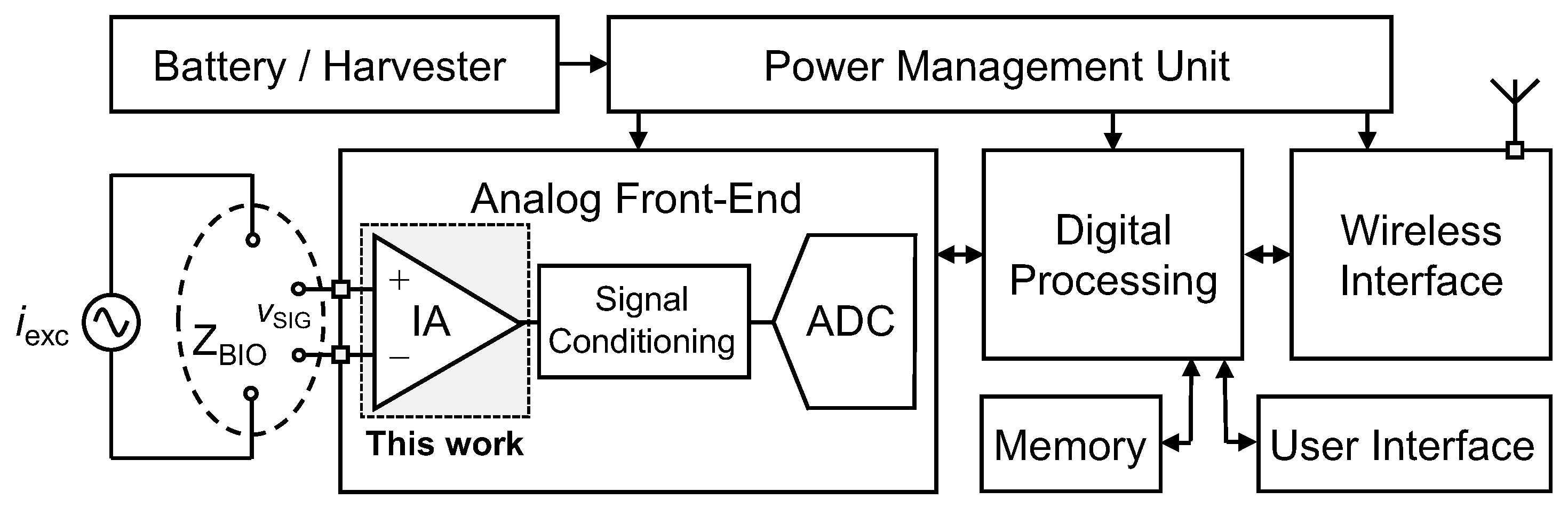
The block diagram of a bioimpedance-based IoT system for medical applications is illustrated in Figure 1. The source of power, which can be a battery or an energy harvester, is controlled by a power management unit (PMU), which optimizes and regulates the signals used to supply the rest of the blocks. The bioimpedance under test, Z B I O , is excited by an AC signal, usually a current in order to avoid any damage on the biological sample, and the resulting voltage is acquired and conditioned by the analog front-end (AFE). Then, signals are efficiently processed in the digital domain, by a digital signal processor (DSP), and can be locally stored or transmitted by means a wireless protocol. The user interface allows control of the operation of the overall system.
The IA is a critical constituent block of the system previously described [4,5,6,7,8,9,10,11,12,13,14,15,16,17,18,19,20,21,22,23,24,25,26,27,28,29]. Indeed, an appropriate signal acquisition is required, which includes a demanding performance in terms of differential-mode (DM) signals amplification, common-mode (CM) signals rejection, and noise, among others, whereas the overall power consumption has to be kept to a minimum extent, which is particularly a challenge in applications that require the processing of signals contained in a wide frequency range and with a relatively large amplitude. The indirect current feedback (ICF) technique results suitable to design a monolithic IA with low-voltage capability [5,22,29]. In addition, a single-stage ICF IA provides compactness and the possibility of achieving operation over a broad frequency range [11,12,22,26,29].
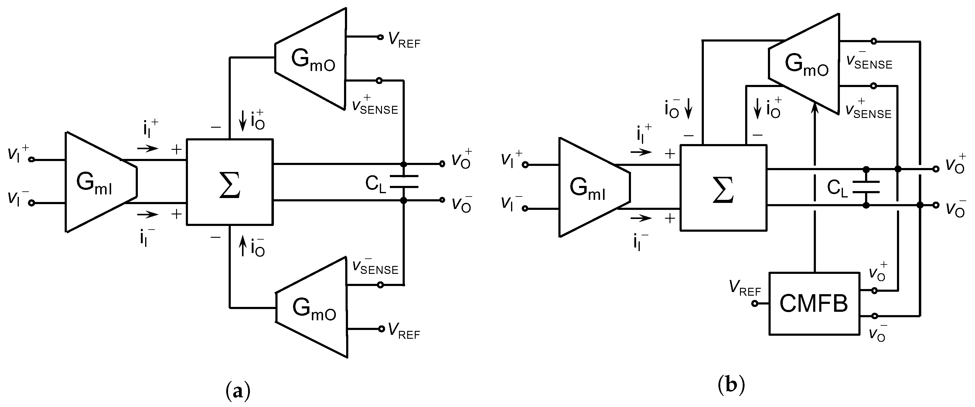
The overall performance of an analog system in general, and of an IA in particular, can be enhanced by adopting a fully differential (FD) implementation [23,25,30]. There are well-known advantages associated to this solution, such as the extension of the signal range, due to the availability of two output terminals, the increase of the linearity, thanks to the ideal cancellation of even-order harmonics, and the decrease of the effects of undesired noises coming from the supply, which can be considered as CM signals. There are also disadvantages related to the use of a FD circuit, such as the increase of the circuitry to obtain a fully symmetrical structure, with the consequent increase in area and power consumption, or the need of a CM feedback (CMFB) network, to control the CM component of the output signal. Therefore, all the pros and cons must be considered and a design tradeoff has to be established.
A FD IA, relying on the ICF technique and suitable for bioimpedance analysis in an IoT biomedical application, is presented in this contribution. An analysis of the main characteristics of the proposed circuit is provided, which is confirmed by means of simulated and experimental results. In addition, the solution is compared in terms of circuit structure to other differential IA previously reported [29], whereas a performance comparison with similar solutions in the literature is also carried out. The circuit has been designed and fabricated in 180 nm CMOS technology to operate with a single-supply voltage of 1.8 V. The experimental characterization illustrates the robustness of the proposed solution. The rest of the manuscript has been organized as follows. Section 2 deals with the block diagram and the transistor level implementation of the IA, whereas different design considerations are discussed in Section 3. Measurement results are reported in Section 4 and conclusions are drawn in Section 5.

2. Principle of Operation

The block diagram of the proposed FD IA is described in order to clearly understand the role of each constitutive section. In addition, the transistor level implementation of both the core of the IA and the CMFB network are also detailed.

2.1. Block Diagram

Different approaches to implement a differential IA have been previously reported [9,17,18,19,20,23,24,25,29]. Among them, there are solutions based on the ICF technique, as the pseudo-differential (PD) IA proposed in [29], the block diagram of which is illustrated in Figure 2a. The sections G m I and G m O are an input and an output (or feedback) transconductor, used, respectively, to process the input signal and establish the current feedback. When the input signal, v I , D M , is applied to the transconductor G m I , a current i I is generated. Similarly, an output current i O is produced when the voltage v S E N S E V R E F is applied to the input terminals of the voltage-to-current (V-to-I) converter G m O . The voltage v S E N S E is used as feedback signal and V R E F is a reference voltage used to set the DC component of v O to the intended level. In the particular case of Figure 2a, a single-stage structure is represented, in which an unitary feedback loop is established. Indeed, the output voltages, v O + and v O , are shorted to the feedback terminals, v S E N S E + and v S E N S E , whereas two copies of the block G m O are required to stablish the differential feedback loop. The feedback action around each output transconductor controls individually the DC level at the two output terminals and; hence, no CMFB is needed.
The block diagram of the proposed FD IA is depicted in Figure 2b. As observed, the feedback network is implemented differentially and, hence, only one output transconductor is required. Nevertheless, it is well known that the establishment of a differential feedback loop relies on the assistance of a CM control network, in order to dynamically set the CM component of the output voltage to the intended level. With this purpose, the CMFB section illustrated in Figure 2b has been included. As observed, the DC component of the output voltage is induced to be equal to V R E F by the CMFB circuit, rather than being applied to the output transconductor, as it is done in the PD structure in Figure 2a. The existence of well-differenced signal paths for the DM and CM components in the FD approach allows the individual optimization of their response, which is not possible in the PD solution, where the control of the output CM voltage is embedded in the implementation of the output section of the circuit.
A hand analysis of the block diagram in Figure 2b led to the following transfer function for the system:
H ( s ) v o ( s ) v i ( s ) = G m I · R o u t 1 s C L 1 + G m O R o u t 1 s C L
where R o u t and C L are the output resistance and the load capacitance, respectively, of the summing stage. Assuming a high gain for the loop around the transconductor G m O , the voltage gain, A v , and the BW of the IA are inferred from (1) and can be expressed as:
A v v o v i , d m = G m I G m O
B W = G m O C L
The voltage gain of the IA is adjusted by means of the ratio of G m I and G m O . In addition, a proper value of C L has to be selected in order to ensure an optimal phase margin and, hence, appropriate frequency and time responses.

2.2. Transistor Level Implementation

The transistor level implementation of the proposed FD IA is illustrated in Figure 3, where the different circuit sections are labelled at the bottom. The V-to-I conversion at the input (output) transconductor is carried out by a resistor and two voltage followers. The input (output) voltage is applied to resistor R I ( R O ) through two super-source-follower (SSF) sections, which act as voltage buffers. The SSF block incorporates an implicit feedback loop, implemented by transistors MDI and MFI (MDO and MFO), that reduces the effective output resistance of the block and makes its voltage gain very close to unity, regardless of the value of the linearization resistor. As a result, the value of R I ( R O ) can be greatly reduced without hardly affecting the operation of the SSF sections, which allows a reduction in the noise contribution of the resistor to be made, as well as the silicon area occupied by this passive component. The SSF structures are biased by means of devices MSUI and MSDI (MSUO and MSDO), which are single-transistor current sources providing tail currents 2 I B and I B , respectively. The gate terminals of these transistors are connected to the corresponding bias voltage, V B N or V B P , in the biasing network represented at the left of Figure 3. Capacitors C C 1 to C C 4 are used to optimize the phase margin of the feedback loop inherent in each SSF cell. The effective transconductance of the input and output V-to-I cells is equal to:
G m , e f f i v D M = 2 R 1 1 + 1 + 2 R 1 g m , M D g o , M D + g o , M S D g m F 2 R
where g m , M i and g o , M i are the transconductance and output conductance, respectively, of transistor Mi, at the input and the output transconductor, R is the linearization, or source degeneration, resistor ( R I or R O ), and g m g o has been assumed. The factor of 2 in (4) indicates that the current signal generated in the input and the output transconductor, i I and i O , respectively, is conveyed to the output terminals of the IA by the two branches of the circuit section. In addition, the second term in (4), multiplying the main contribution 2 / R , represents the load regulation effect of resistor R on the voltage buffers. In first order of approximation, the effective transconductance of each V-to-I converter is approximately equal to two times the inverse of the linearization resistor.
The current signals generated at G m I and G m O are mirrored to the output nodes of the IA by using current mirrors with gains 1 : 1. Cascode transistors are used in the output branches in order to increase the output resistance and, hence, the open-loop voltage gain. In addition, cascode devices MFCI and MFCO are used in G m I and G m O , respectively, to ideally cancel out the systematic offset in the current reflections. Additional design flexibility to adjust the voltage gain and bandwidth of the IA to the intended values can be obtained by sizing the current mirrors with a gain different from unity [29]. The voltage gain and the BW of the proposed IA can be specified by considering the general expressions (2) and (3), along with the equation of the effective transconductance in (4), and can be rewritten as:
A v R O R I
B W 2 C L R O
The input CM voltage of the FD IA in Figure 3 can be adjusted over a reasonably wide range. Indeed, the operation for input signals around the midsupply is ensured by adequately setting the aspect ratio of the input devices, so that the upper current source transistors, MSUI, can operate in saturation. Thus, the maximum level of the input CM voltage that can be achieved close to V D D is constrained by the operation in saturation of transistors MSUI. Furthermore, the operation for v I , C M around ground can be easily achieved by proper sizing of transistors MFI. Indeed, the voltage at the drain of transistors MDI, which could force their operation in the triode region, can be reduced to an appropriate level by increasing the aspect ratio of transistors MFI, thus ensuring the operation of the input drivers in saturation.
The structure of the CMFB network used to control the DC level of the output voltage is depicted in Figure 4. A current-mode approach, based on generating a CM current signal that is a function of the output CM voltage, has been followed. The output voltages of the FD IA are used as input signals in the CMFB section and are applied to the inputs of two cross-coupled differential pairs. The other two input terminals of the CMFB are connected to the reference voltage V R E F . Assuming the voltage difference v O + v O small and, hence, the differential pairs operating within their linear region, a current signal i c m , proportional to the output CM voltage, is generated. This current, superimposed to a DC level nominally equal to 2 I B , is mirrored by a NMOS and a PMOS current mirror and injected into the FD IA through the terminal v C M F B . The CM loop is closed through the output branches of the IA, which are connected to the input of the CMFB network. The action of the feedback loop forces the CM component of the output voltage to be equal to V R E F , setting the DC level of the output voltage to this value. The dominant pole of the feedback loop established for the CM signal is the same to that of the DM loop and is determined by the load capacitor. The secondary poles in both cases, DM and CM signals, are associated to low impedance nodes, that is, the corresponding time constants are the product of a low resistance, in general the inverse of a transconductance, and a parasitic capacitance. As a consequence, the frequency compensation of the DM and CM loops in the FD IA can be easily achieved by properly setting the value of the load capacitor. Indeed, the value of C L must be adjusted to have a phase margin higher than 60° in both the CM and the DM feedback loop.

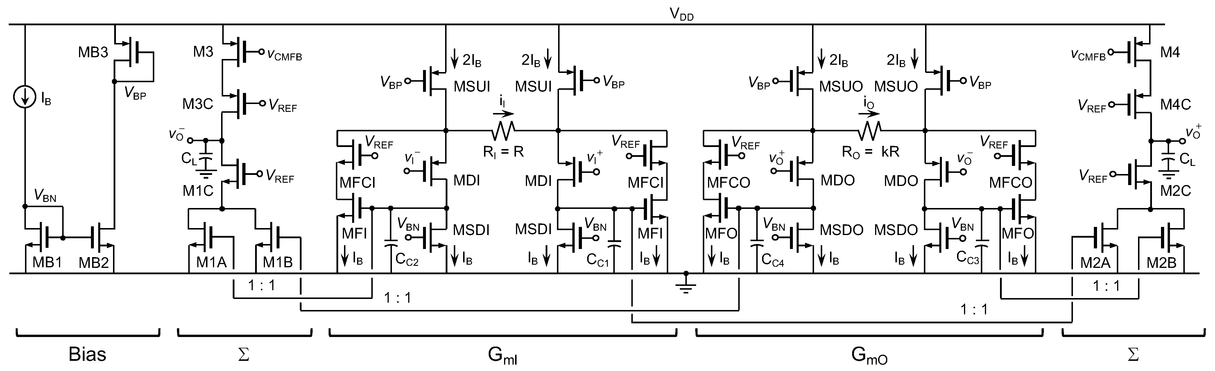
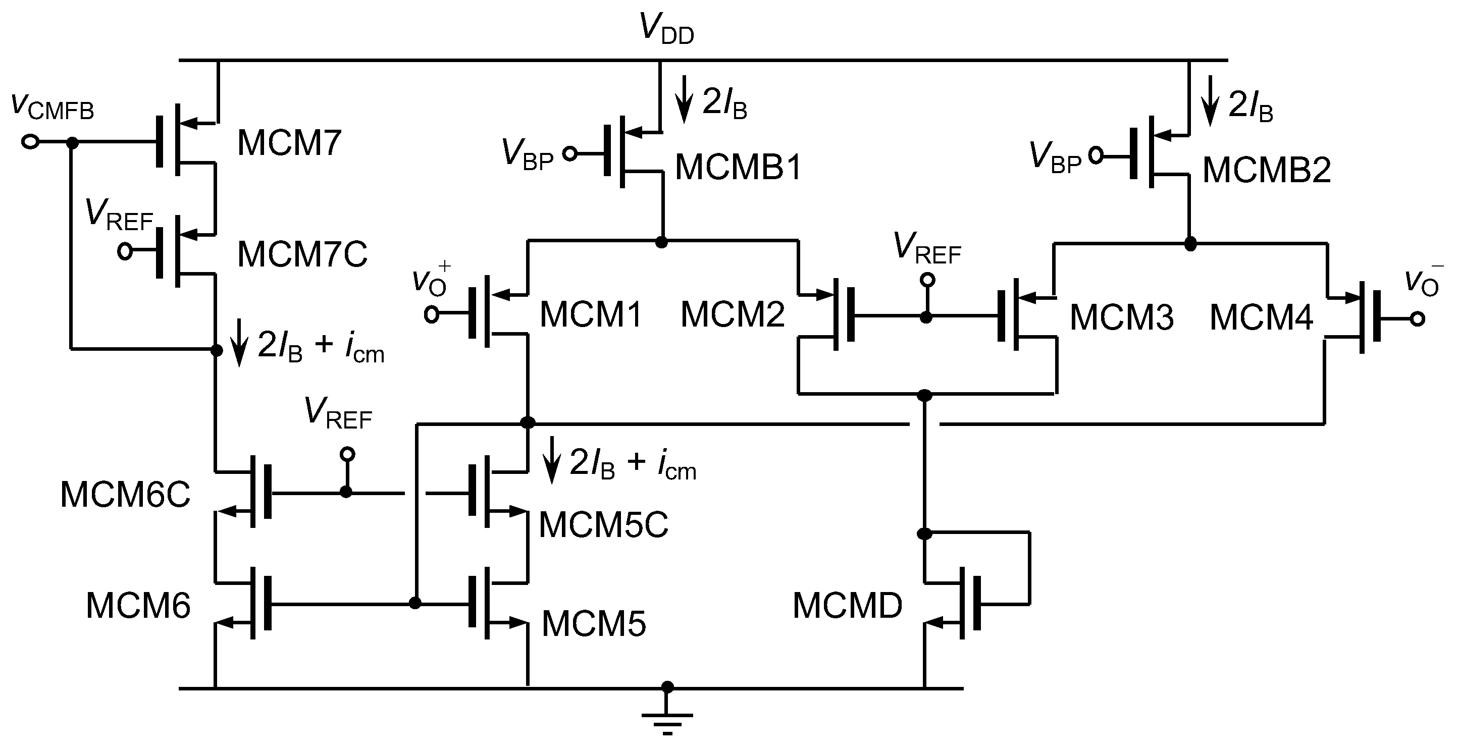
3. Design Considerations

The main features of the FD IA proposed are analysed and discussed in view of the fundamental performance, in order to facilitate the design procedure. In a FD implementation, the CM signal must be processed at least with the same accuracy and speed as the DM signal. Therefore, the CMFB network, in particular, and the CM feedback loop, in general, must be designed so that the open-loop gain (LG) and gain-bandwidth product (LGBW) of both components are similar [30]. This requirement can be analytically expressed as
L G C M L G D M
L G B W C M L G B W D M
Therefore, it is recommendable to provide similar paths to the DM and the CM signal in order to accomplish these requisites. In the case of the IA represented in Figure 3 and Figure 4, the output branch of the core circuit (Figure 3) is common to both the DM and the CM section. Nevertheless, the differential input stage of each loop, and hence the corresponding effective transconductance, is different in every case. Indeed, for the DM signal, the input transconductance is given by (4), whereas for the CM component the transconductance is equal to the individual transconductances of transistors MCM1 to MCM4 in Figure 4. As the linearization carried out in G m I implies a reduction of the transconductance value, it is expected that effective input transconductance of the DM loop is lower as compared to the CM loop. This fact ensures that an appropriate treatment of the DM signal will result in an adequate processing of the CM signal.
Regarding the signal processing of the FD IA, only the DM component gives rise to an output current in the input and output V-to-I converters, being the CM signal rejected by the differential structure of these stages. However, a CM signal can also produce an output current, given that the presence of mismatches is unavoidable in a real implementation. In order to evaluate the impact of the join action of a CM signal and the mismatches on the output current produced, the residual transconductance of the input and the output transconductor in the IA, defined as Δ G m i v C M , has been analytically calculated. With this purpose, each small signal parameter g i has been assumed to have values equal to g i + Δ g i / 2 and g i Δ g i / 2 for a given pair of ideally matched transistors. In addition, the contributions to the residual transconductance, due to considering mismatches in every pair of transistors, have been evaluated individually. The corresponding expressions were obtained by means of a hand analysis and the main terms were determined by simulations, resulting to be dominant the responses associated to mismatches in the transconductance ( Δ g m ) and output conductance ( Δ g o ) of the input driver transistors, MDI and MDO. The corresponding expressions are:
Δ G m | Δ g m , M D 2 R · Δ g m , M D g o , M D g m , M D 2 · 1 1 + 2 R 1 g m , M D g o , M D + g o , M S D g m , M F
Δ G m | Δ g o , M D 2 R · Δ g o , M D g m , M F · 1 1 + 2 R 1 g m , M D g o , M D + g o , M S D g m , M F
where MD represents the driver transistors in G m I and G m O . The impact of the transconductance and output conductance mismatches of other transistors on Δ G m is negligible and, hence, is not reported here for the sake of conciseness.
The use of the CM rejection ratio (CMRR) is a very widespread habit in order to compare the magnitude of the CM gain with respect to the DM gain. As the proposed IA has a single-stage structure, the voltage gain for DM and CM signals will be given by the product of the input transconductance and the output impedance. Assuming the same output impedance for both signal components, the CMRR of the IA can be expressed in terms of the ratio of the effective and the residual transconductance, given respectively by (4) and (8b), as:
C M R R G m I Δ G m I = 1 Δ g m , M D I g o , M D I g m , M D I 2 + Δ g o , M D I g m , M F I · 1 + 2 R I 1 g m , M D I g o , M D I + g o , M S D I g m , M F I 1 + 1 + 2 R I 1 g m , M D I g o , M D I + g o , M S D I g m , M F I
The most-right term in (9) represents the ratio of the load regulation effects of resistor R for the CM and the DM signals, respectively. Thanks to the improved response of the SSF cell, the value of these terms is very close to unity, which allows the expression of the CMRR as a function of the different mismatches in the actual implementation of the circuit. At this point it is worth to mention that, as observed in Figure 2, the structure of the input section of both the PD IA and the FD IA is the same and, hence, both structures present a similar rejection to CM signals form the architecture point of view.
Another key parameter for an IA is the noise, as it indicates the minimum signal level that can be processed. In the case of an IA for bioimpedance spectroscopy, the signal bandwidth required is usually wide and, hence, thermal noise is dominant. The spectral density of the input referred thermal noise has been analytically determined, assuming that the main contributions are due to the input V-to-I converter, and can be expressed as:
v i N , t h 2 Δ f = 1 + 1 + 2 R I 1 g m , M D I g o , M D I + g o , M S D I g m , M F I 2 · 4 k T R I · 1 + 4 3 g m , M D I + g m , M S U I R I
where k and T are Boltzmann’s constant and the absolute temperature, respectively. The first term in (10) represents the conversion factor for referring the noise from the resistor to the input of the circuit, and is the inverse of the load regulation effect of resistor R I on the SSF cell (see Equation (4)), the second factor is the thermal noise of resistor R I , and the last term includes the main thermal noise contributions of the devices involved in the circuit implementation of the input V-to-I converter, G m I . It can be inferred from (10) that the noise of the IA can be decreased by reducing the value of the source degeneration resistor R I , which is possible until a certain limit thanks to the use of SSF sections.
The fact of linearizing the V-to-I converters in the IA by means of a resistor, requires a given level of biasing current to achieve a given input DM voltage range with a determined linearity. In each SSF cell in the input and output transconductors, the bias current 2 I B is split into two branches corresponding to the input and feedback transistors. As the tail current of the driver devices is fixed to I B by the lower current sources, a current equal to I B is steered towards the feedback transistors. Consequently, the maximum input DM signal that can be processed by each V-to-I converter is that leading to a current equal to zero through one of the feedback transistors. This condition can be expressed for G m I as
v I , D M m a x = ± R I · I B
where the voltage gain of the SSF cells has been assumed to be equal to unity. Nevertheless, this is an extreme situation that leads to switching off one of the branches of the input transconductor. Instead, a specific criterion, such as considering a given total harmonic distortion (THD) level, is assumed in a practical case to determine the value of v I , D M m a x in an objective way.

4. Experimental Results

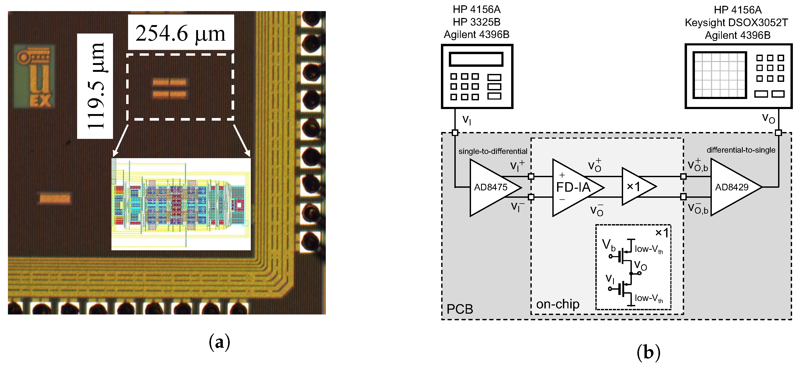
The fully-differential IA illustrated in Figure 3, along with the CMFB section in Figure 4, has been designed and fabricated in 180 nm CMOS technology to operate with a single-supply voltage of 1.8 V. The microphotograph of the chip, including details on the layout, is depicted in Figure 5a, and the aspect ratios of the main transistors in the circuit are reported in Table 1. The measurements have been carried out over 10 samples of the silicon prototype. The testbench implemented for the experimental characterization is represented in Figure 5b, where the on-chip and the PCB levels have been highlighted. An on-chip differential voltage buffer, referred to as ×1, has been included for test purposes in order to isolate the output terminals of the FD IA from heavy loads. The buffer consists of two PMOS source followers including low- V t h transistors, so that operation with the general 1.8-V supply is possible. Auxiliary circuits AD8475 and AD8429 in Figure 5b are used to carry out, respectively, a single-to-differential signal conversion at the input of the IA and a differential-to-single signal conversion at the output in order to facilitate measurements. Even though these commercial components have been selected with a bandwidth higher that the circuit under test, their influence on the measurement procedure is unavoidable. The value of the reference voltage V R E F used to set the DC level of the output voltage was set to 0.9 V. In addition, this voltage is also used to bias the gate terminal of the cascode transistors. The biasing current of each V-to-I converter, i.e., G m I and G m O , was adjusted as I B = 10 μ A. The source degeneration resistors R I and R O were implemented with non-salicided high-resistance polysilicon having values equal to R I = 5 k Ω and R O = 20 k Ω , thus leading to a nominal voltage gain of 4 V/V (12.04 dB).
The load capacitors, C L , were built on-chip as metal-insulator-metal devices to make stable the feedback loop established around the transconductor G m O 
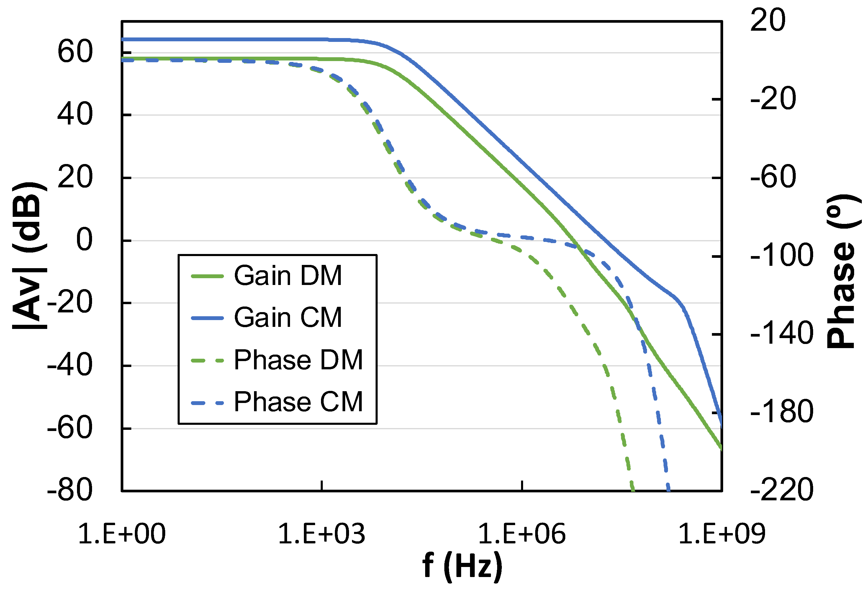
. The design criterion selected was to ensure a phase margin of 60° considering the nominal value of the load capacitors, equal to 1.33 pF each, and the parasitic capacitance also connected to the output terminals due to the test buffer. In addition, it is worth to point out that the effective value of the parasitic capacitance introduced by the test buffer slightly relies on the value of the total external capacitance, associated to the PCB and the test probe used for measurements. This external capacitance has been estimated to be around 30 pF in most of the test configurations followed. Under these conditions, the open-loop frequency response of the DM and CM signal paths has been simulated and is represented in Figure 6. For the DM signal L G D M = 58.0 dB and L G B W D M = 5.9 MHz with a phase margin of 52.8° and a gain margin of 17.6 dB, whereas the CM signal response provides L G C M = 64.2 dB and L G B W D M = 18.1 MHz with a phase margin of 75.5° and a gain margin of 14.3 dB. These results show the stability of both the DM and the CM feedback loop and confirm the requirements imposed in (7a) and (7b) to the CM signal path. The bandwidth of the CM signal is noticeably higher than that of the DM component. This is due to the fact that the linearization carried out in the input differential structure of the IA leads to a lower effective transconductance as compared to the CMFB section, which results in a narrower frequency range.
The DC measurements on the 10 available samples allowed to obtain an average DC supply current for the IA equal to 266.4 μ A, with a standard deviation of 2.6 μ A. The DC voltage level shift introduced by the on-chip buffer did not allow characterizing the actual output voltage of the IA, expected to be very close to V R E F 
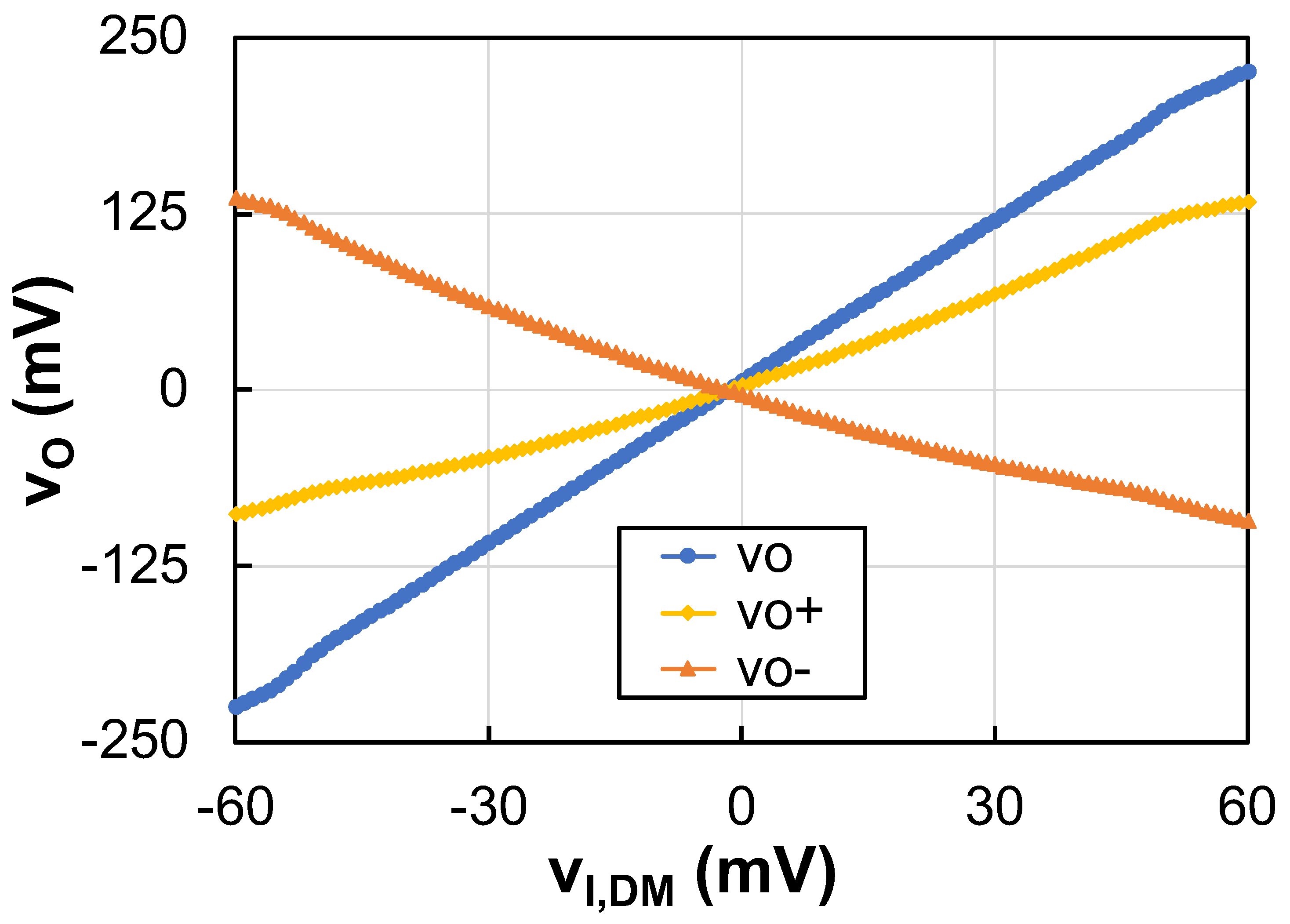
. Hence, only the standard deviation of the buffered output voltage, equal to 3.63 mV, is reported in order to determine the variability of the output voltage among the different samples. The experimental v I v O DC transfer characteristic of the IA is represented in Figure 7. The CM level of the output voltage, defined as ( v O + + v O ) / 2 , has been used to shift all plots from their original DC level down to zero, so that results can be more easily interpreted. A linear voltage range at DC larger than ±50 mV can be inferred for the differential output response. As observed in Figure 7, the non-linearity appreciable in v O + and v O is cancelled out when the overall output signal is obtained as the difference of the individual responses, i.e., v O = v O + v O .
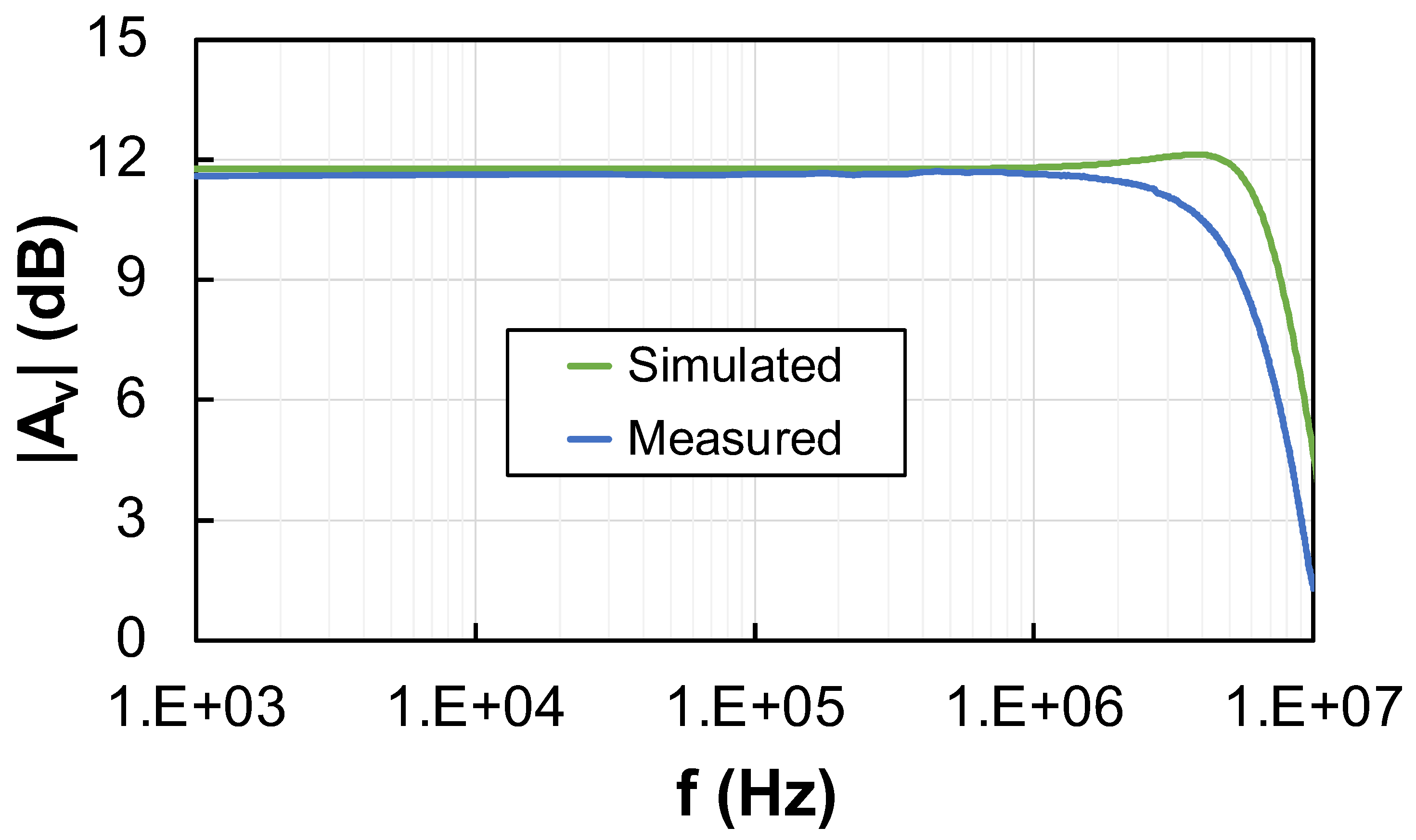
The simulated and experimental frequency response of the IA is illustrated in Figure 8, where the magnitude of the DM voltage gain is depicted. From the experimental response the voltage gain in the passband, A v , and the BW of the IA can be extracted, obtaining values equal to 3.78 V/V (11.4 dB) and 5.83 MHz, respectively. The gain value is in close agreement with the design value of 4 V/V or 12.4 dB (relative error of 5.0%) and with the simulated value of 3.69 V/V or 11.34 dB (relative error of 2.4%), whereas the measured BW deviates from the corresponding simulated value, equal to 7.76 MHz (relative error of 24.8%). The difference between the simulated and the experimental responses in Figure 8 has two possible reasons. On the one hand, it has been found that the on-chip voltage buffer is more sensible to external load capacitors than expected from simulations. On the other hand, the BW of the IA is determined by the on-chip load capacitors illustrated in Figure 3, the value of which can suffer important absolute variations during the fabrication process. The nominal simulated value of the BW has been complemented with the result extracted from a 1000-run Montecarlo analysis, considering mismatch and process variations, which has been found to be equal to 10.27 ± 4.70 MHz. Considering the standard deviation as a suitable error margin, the lower bound of the statistically simulated BW encloses the values of both the nominally simulated and the measured BW. The time response of the proposed IA, depicted in 
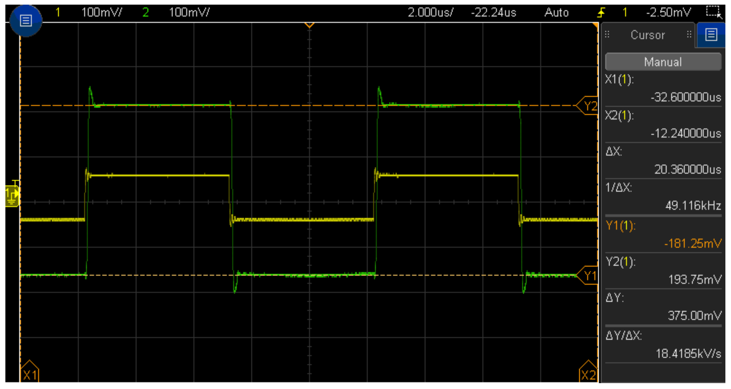
Figure 9, has been used to confirm its stability. In particular, a 100-mV p p input signal (yellow plot) is applied and an appropriate establishment of the output voltage (green plot) can be observed.
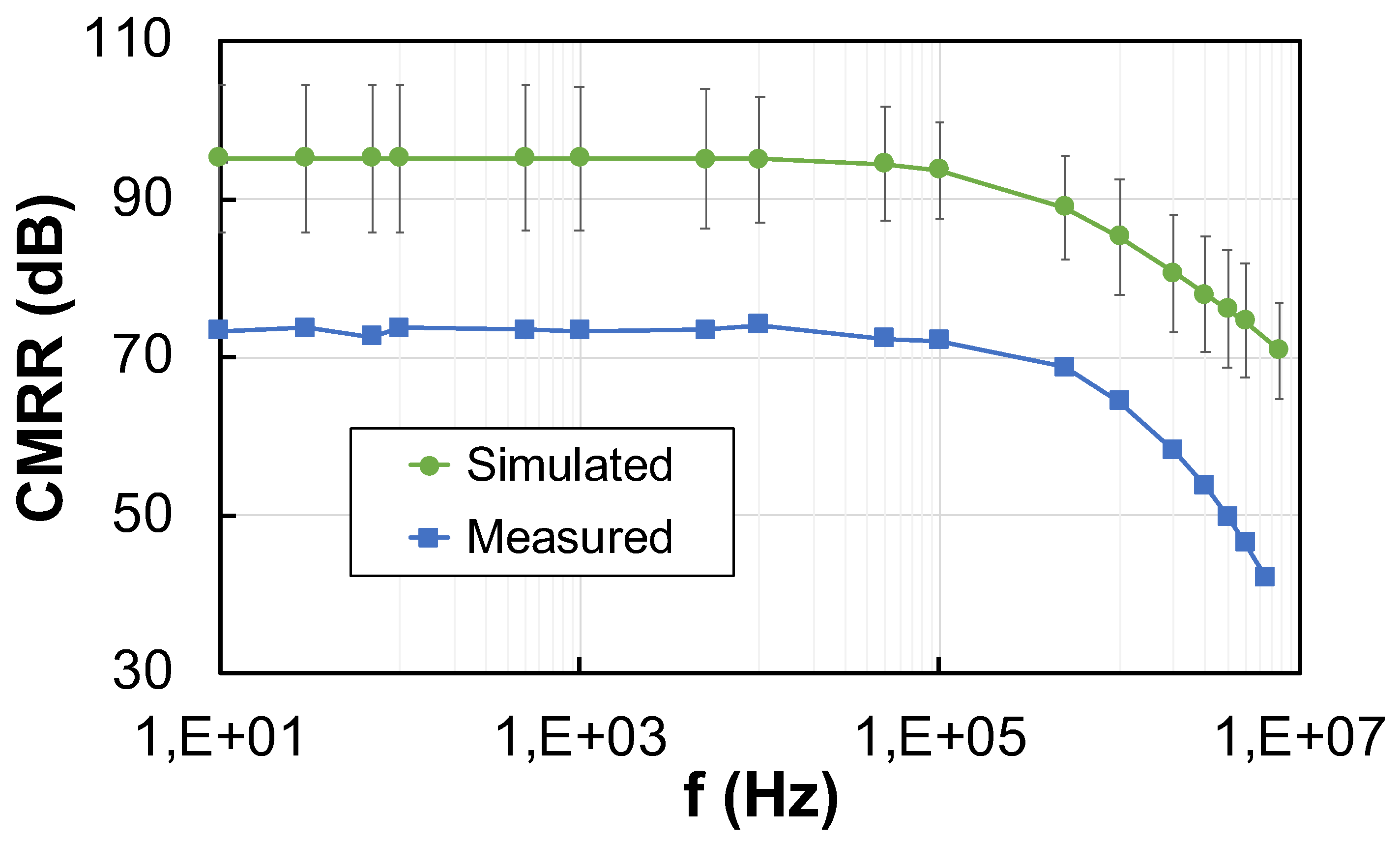
The response to CM signals has also been obtained. The CMRR has been simulated and measured as a function of the frequency of the input signal and is shown in Figure 10. In the simulated plot (in green color), the average value, extracted from a 1000-run Montecarlo analysis including mismatch and process variations, is represented, whereas the error bars indicate the standard deviation, σ . As observed, the experimental CMRR lays below the error margin when the standard deviation is considered, but it has been proved that is enclosed by a 3- σ 
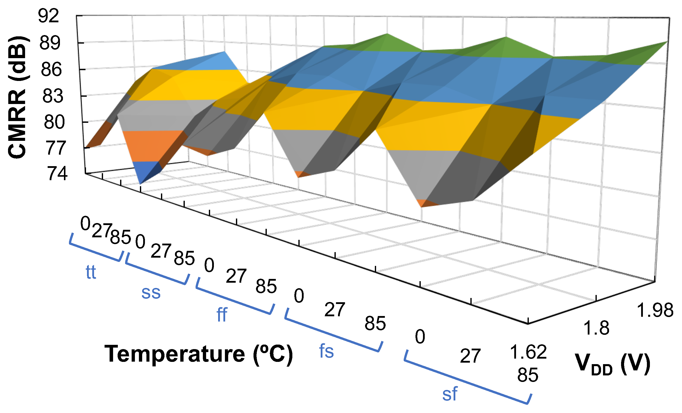
error region. The measured CMRR at low frequencies and at the frequency of the BW is equal to 73.3 dB and 42.0 dB, respectively. Furthermore, the impact of process, voltage, and temperature (PVT) variations on the CMRR at DC has been determined by nesting a 100-run Montecarlo analysis and a corner analysis. In particular, typical-typical (tt), slow-slow (ss), fast-fast (ff), fast-n-slow-p (fs), and slow-n-fast-p (sf) corners were considered for the active devices, whereas the temperature was set to values (0,27,80) °C and the supply voltage was adjusted to (1.62,1.8,1.98) V, i.e., a variation equal to ±10% was assumed. The corresponding results are summarized in Figure 11, where in the axis corresponding to the temperature the considered range has been replicated for each corner of the active devices. As observed, the CMRR varies between 74.8 dB and 90.5 dB.
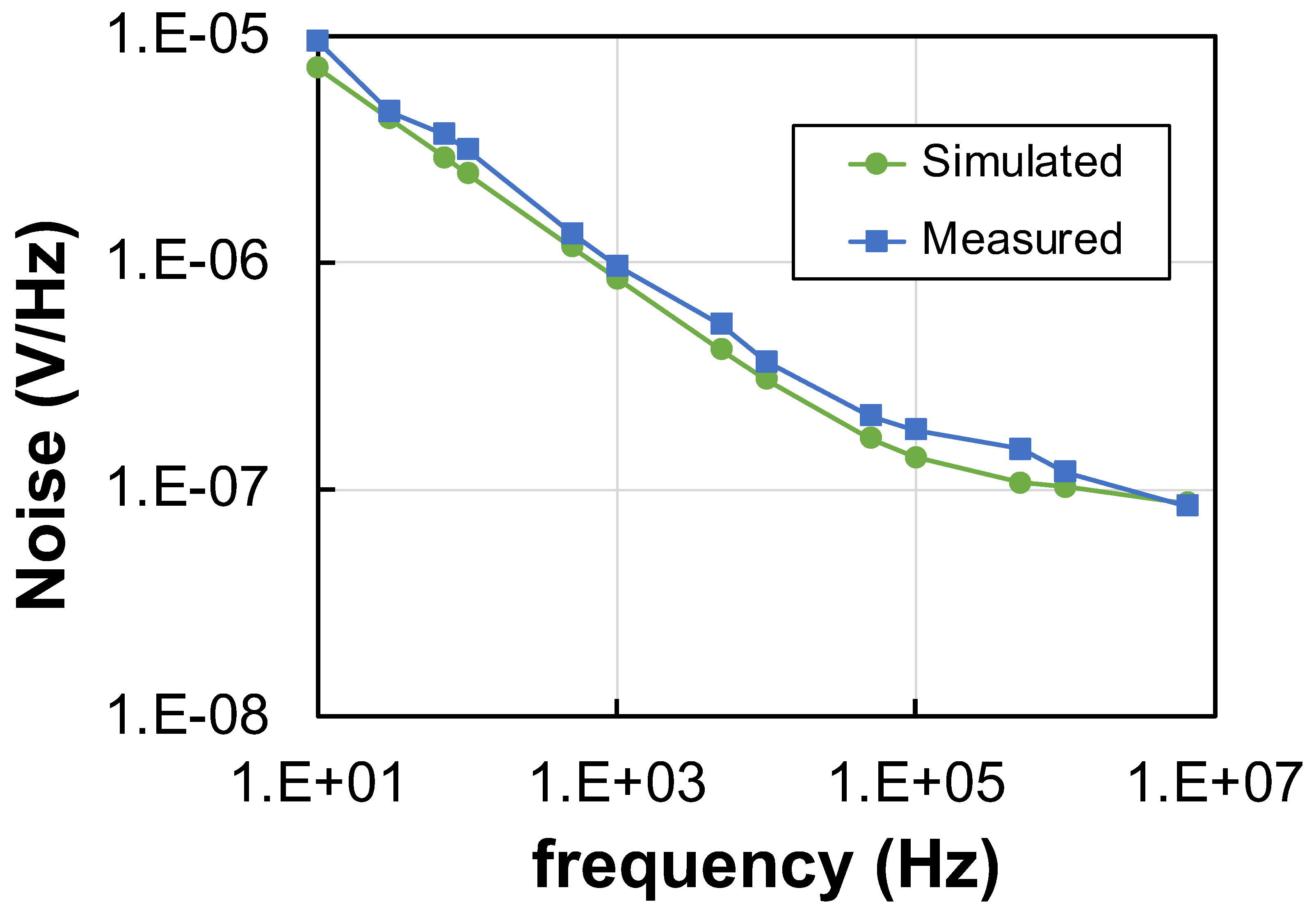
The noise response of the FD IA has also been characterized. In particular, the spectral density of noise has been simulated and measured and is depicted in Figure 12. In addition, the noise has been integrated over a frequency band between 100 Hz and the frequency of the BW, obtaining a value equal to 86.4 μ V r m s . The calculated experimental noise is slightly higher than the actual value, due to the finite approximation followed to integrate the noise. In any case, the simulated noise, equal to 74.7 μ V r m s (relative error of 15.7%), is much lower. The reason of the noise increase in measurements is ascribed to the experimental setup and to the contributions of the different auxiliary circuits used for the test, as illustrated in Figure 5b and already indicated at the beginning of this section. The THD has been used to asses the linearity of the dynamic response of the FD IA. In Figure 13 the simulated and experimental THD of the output voltage is represented as a function of the input DM signal amplitude for frequencies of 1 kHz and 10 kHz. The simulated THD is reduced as compared to the experimental response for small values of the input signal due to the lower noise floor level in simulations. Nevertheless, for high input signals the measured response results even more linear. Using the widespread criterion of considering the 1%-THD as a limit to determine the maximum input signal that can be processed with reasonable linearity, experimental values of 59.6 mV and 57.6 mV were obtained for input frequencies of 1 kHz and 10 kHz, respectively.
The performance of the designed and fabricated FD IA is summarized in Table 2, where simulated and measured results are reported. The data expressed as the mean value plus/minus the standard deviation were obtained from a 1000-run Montecarlo analysis with mismatch and process variations in the case of simulations and from the measurements on 10 samples in the case of experimental results. In general, there is a good agreement between the simulated and the measured metrics, being the corresponding differences due to the variations of the process parameters during fabrication. One exception is the case of the noise, which, as discussed previously, greatly increases in measurements with respect to simulations.
The comparison of the previous metrics for different IAs is done usually in terms of a widespread figure-of-merit (FoM) known as noise efficiency factor (NEF) [4]. This parameter indicates how large is the noise of a system as compared to the white noise of a single MOS transistor with the same drain current and bandwidth, and is defined as:
N E F = V i N , r m s 2 I D D π V T 4 k T B W
where I D D and V T are the supply current of the IA and the thermal voltage, respectively. Nevertheless, this parameter does not take into account the amplitude of the signals to be processed. Indeed, when large input signals must be handled, a high biasing current is required, thus resulting in a penalty in therms of NEF. In this case, the dynamic range (DR), defined as
D R = 20 · log v I , D M m a x V i N , r m s
can be used as a complementary FoM for performance comparison.
The FD IA presented is compared in Table 3 to other works previously reported and with similar characteristics, i.e., based on current feedback and presenting a wide bandwidth. The work by Worapishet et al. [11] presents very good values of NEF and DR, especially considering that measured results are given, but the BW is more limited than in the other solutions. The IAs in [12,22] have a good response in general, even tough they are solutions supported by simulated results. In [26] a very high bandwidth is achieved but no data regarding the size of the processed signals and the noise are reported. The IA proposed in [29] has also a differential structure and achieves a higher BW than the IA proposed here, but the signal processed are smaller and the noise is higher, thus resulting in a higher NEF and a lower DR. The proposed IA has a BW suitable for electrical bioimpedance analysis and is able to process the largest input differential signals for similar supply currents. In addition, it is a compact solution in terms of silicon area as compared to most of the other solutions, especially considering that it has a FD structure. Finally, it is worth to point out that the increase of the experimental noise, previously indicated, leads to a noticeable reduction of the measured DR and to an increase of the experimental value of the NEF. Indeed, the simulated characterization of the IA reported values for the NEF and the DR equal to 14.6 and 57.1, respectively.

5. Conclusions

An IA suitable for bioimpedance-based IoT applications and based on the ICF technique has been presented. The SSF structure has been incorporated in the design of the IA in order to reduce input referred noise and silicon area. In addition, a FD implementation has been selected to enhance the overall performance of the circuit. The proposed ICF FD IA been designed and fabricated in 180 nm CMOS technology to operate with a supply voltage of 1.8 V and provide a voltage gain of 4 V/V. Measurements on 10 different samples of the silicon prototype showed wide bandwidth, high CMRR and linear signal processing, thus confirming the suitability of the proposed solution for the intended application.

Author Contributions

Conceptualization, I.C., J.M.C. and J.L.A.; methodology, I.C., J.M.C. and J.L.A.; software, I.C. and J.M.C.; formal analysis, J.M.C. and R.P.-A.; investigation, I.C., J.M.C. and J.L.A.; resources, I.C., J.M.C. and M.Á.D.; data curation, I.C., J.M.C., M.Á.D. and R.P.-A.; writing—original draft preparation, I.C., J.M.C. and J.L.A.; writing—review and editing, I.C., J.M.C., J.L.A., M.Á.D., R.P.-A. and J.F.D.-C.; visualization, I.C. and J.M.C.; supervision, J.M.C. and J.L.A.; project administration, J.F.D.-C.; funding acquisition, J.L.A. and J.F.D.-C. All authors have read and agreed to the published version of the manuscript.

Funding

Work funded by projects RTI2018-095994-B-I00, from MCIN/AEI/10.13039/501100011033, and IB18079, from Junta de Extremadura R&D Plan, and by Fondo Europeo de Desarrollo Regional (FEDER) Una manera de hacer Europa. Silicon samples granted by EUROPRACTICE MPW and design tool support.

Conflicts of Interest

The authors declare no conflict of interests.

References

  1. Minhee, K.; Eunkyoung, P.; Hwan, C.B.; Kyu-Sung, L. Recent Patient Health Monitoring Platforms Incorporating Internet of Things-Enabled Smart Devices. Int. Neurourol. J. 2018, 22, S76–S82. [Google Scholar]
  2. Gope, P.; Gheraibia, Y.; Kabir, S.; Sikdar, B. A Secure IoT-Based Modern Healthcare System With Fault-Tolerant Decision Making Process. IEEE J. Biomed. Health Inf. 2021, 25, 862–873. [Google Scholar] [CrossRef] [PubMed]
  3. Grimnes, S.; Martinsen, V.G. Bioimpedance and Bioelectricity Basics, 3rd ed.; Academic Press: Cambridge, MA, USA, 2015. [Google Scholar]
  4. Steyaert, M.S.J.; Sansen, W.M.C. A micropower low-noise monolithic instrumentation amplifier for medical purposes. IEEE J. Solid-State Circuits 1987, 22, 1163–1168. [Google Scholar] [CrossRef]
  5. van den Dool, B.J.; Huijsing, J.K. Indirect current feedback instrumentation amplifier with a common-mode input range that includes the negative rail. IEEE J. Solid-State Circuits 1993, 28, 743–749. [Google Scholar] [CrossRef] [Green Version]
  6. Martins, R.; Selberherr, S.; Vaz, F.A. A CMOS IC for portable EEG acquisition systems. IEEE Trans. Instrum. Meas. 1998, 47, 1191–1196. [Google Scholar] [CrossRef]
  7. Harrison, R.R.; Charles, C. A low-power low-noise CMOS amplifier for neural recording applications. IEEE J. Solid-State Circuits 2003, 38, 958–965. [Google Scholar] [CrossRef]
  8. Zhao, Y.Q.; Demosthenous, A.; Bayford, R.H. A CMOS instrumentation amplifier for wideband bioimpedance spectroscopy systems. In Proceedings of the 2006 IEEE International Symposium on Circuits and Systems, Kos, Greece, 21–24 May 2006; pp. 5079–5082. [Google Scholar]
  9. Yazicioglu, R.F.; Merken, P.; Puers, R.; Van Hoof, C. A 60 μW 60 nV/√Hz readout front-end for portable biopotential acquisition systems. IEEE J. Solid-State Circuits 2007, 42, 1100–1110. [Google Scholar] [CrossRef]
  10. Denison, T.; Consoer, K.; Santa, W.; Avestruz, A.; Cooley, J.; Kelly, A. A 2 μW 100 nV/√Hz chopper-stabilized instrumentation amplifier for chronic measurement of neural field potentials. IEEE J. Solid-State Circuits 2007, 42, 2934–2945. [Google Scholar] [CrossRef]
  11. Worapishet, A.; Demosthenous, A.; Liu, X. A CMOS instrumentation amplifier with 90-dB CMRR at 2-MHz using capacitive neutralization: Analysis, design considerations, and implementation. IEEE Trans. Circuits Syst. I Regul. Pap. 2011, 58, 699–710. [Google Scholar] [CrossRef]
  12. Ramos, J.; Ausín, J.L.; Duque-Carrillo, J.F.; Torelli, G. Wideband low-power current-feedback instrumentation amplifiers for bioelectrical signals. In Proceedings of the International Multi-Conference on Systems, Signals and Devices, Chemnitz, Germany, 20–23 March 2012; pp. 1–5. [Google Scholar]
  13. Abdelhalim, K.; Jafari, H.M.; Kokarovtseva, L.; Velazquez, J.L.P.; Genov, R. 64-channel UWB wireless neural vector analyzer SOC with a closed-loop phase synchrony-triggered neurostimulator. IEEE J. Solid-State Circuits 2013, 48, 2494–2510. [Google Scholar] [CrossRef]
  14. Ong, G.T.; Chan, P.K. A power-aware chopper-stabilized instrumentation amplifier for resistive Wheatstone bridge sensors. IEEE Trans. Instrum. Meas. 2014, 63, 2253–2263. [Google Scholar] [CrossRef]
  15. Van Helleputte, N.; Konijnenburg, M.; Pettine, J.; Jee, D.; Kim, H.; Morgado, A.; Van Wegberg, R.; Torfs, T.; Mohan, R.; Breeschoten, A.; et al. A 345 μW multi-sensor biomedical SoC with bio-impedance, 3-channel ECG, motion artifact reduction, and integrated DSP. IEEE J. Solid-State Circuits 2015, 50, 230–244. [Google Scholar] [CrossRef]
  16. Worapishet, A.; Demosthenous, A. Generalized analysis of random common-mode rejection performance of CMOS current feedback instrumentation amplifiers. IEEE Trans. Circuits Syst. I Regul. Pap. 2015, 62, 2137–2146. [Google Scholar] [CrossRef]
  17. Chang, C.; Zahrai, S.A.; Wang, K.; Xu, L.; Farah, I.; Onabajo, M. An analog front-end chip with self-calibrated input impedance for monitoring of biosignals via dry electrode-skin interfaces. IEEE Trans. Circuits Syst. I Regul. Pap. 2017, 64, 2666–2678. [Google Scholar] [CrossRef]
  18. Rezaeiyan, Y.; Zamani, M.; Shoaei, O.; Serdjin, W.A. A 0.5 μA/channel front-end for implantable and external ambulatory ECG recorders. Microelectron. J. 2018, 74, 79–85. [Google Scholar] [CrossRef] [Green Version]
  19. Nasserian, M.; Peiravi, A.; Moradi, F. A fully-integrated 16-channel EEG readout front-end for neural recording applications. AEU–Int. J. Electron. Commun. 2018, 94, 109–121. [Google Scholar] [CrossRef]
  20. Lee, C.; Song, J. A chopper stabilized current-feedback instrumentation amplifier for EEG acquisition applications. IEEE Access 2019, 7, 11565–11569. [Google Scholar] [CrossRef]
  21. Psychalinos, C.; Minaei, S.; Safari, L. Ultra low-power electronically tunable current-mode instrumentation amplifier for biomedical applications. AEU–Int. J. Electron. Commun. 2020, 117, 153120. [Google Scholar] [CrossRef]
  22. Carrillo, J.M.; Domínguez, M.A.; Pérez-Aloe, R.; de la Cruz Blas, C.A.; Duque-Carrillo, J.F. Low-power wide-bandwidth CMOS indirect current feedback instrumentation amplifier. AEÜ–Int. J. Electron. Commun. 2020, 123, 153299. [Google Scholar] [CrossRef]
  23. Kwon, Y.; Kim, H.; Kim, J.; Han, K.; You, D.; Heo, H.; Cho, D.i.; Ko, H. Fully differential chopper-stabilized multipath current-feedback instrumentation amplifier with R-2R DAC offset adjustment for resistive bridge sensors. Appl. Sci. 2020, 10, 63. [Google Scholar] [CrossRef] [Green Version]
  24. Han, K.; Kim, H.; Kim, J.; You, D.; Heo, H.; Kwon, Y.; Lee, J.; Ko, H. A 24.88 nV/√Hz Wheatstone bridge readout integrated circuit with chopper-stabilized multipath operational amplifier. Appl. Sci. 2020, 10, 399. [Google Scholar] [CrossRef]
  25. Matthus, C.D.; Buhr, S.; Kreißig, M.; Ellinger, F. High gain and high bandwidth fully differential difference amplifier as current sense amplifier. IEEE Trans. Instrum. Meas. 2021, 70, 1–11. [Google Scholar] [CrossRef]
  26. Pérez-Bailón, J.; Sanz-Pascual, M.T.; Calvo, B.; Medrano, N. Wide-band compact 1.8 V-0.18 μm CMOS analog front-end for impedance spectroscopy. IEEE Trans. Circuits Syst. II Express Briefs 2022, 69, 764–768. [Google Scholar] [CrossRef]
  27. Pérez-Bailón, J.; Calvo, B.; Medrano, N. 1.0 V-0.18 μm CMOS tunable low pass filters with 73 dB DR for on-chip sensing acquisition systems. Electronics 2021, 10, 563. [Google Scholar] [CrossRef]
  28. Ashayeri, M.; Yavari, M. A front-end amplifier with tunable bandwidth and high value pseudo resistor for neural recording implants. Microelectron. J. 2022, 119, 105333. [Google Scholar] [CrossRef]
  29. Corbacho, I.; Carrillo, J.M.; Ausín, J.L.; Domínguez, M.A.; Pérez-Aloe, R.; Duque-Carrillo, J.F. Compact CMOS wideband instrumentation amplifiers for multi-frequency bioimpedance measurement: A design procedure. Electronics 2022, 11, 1668. [Google Scholar] [CrossRef]
  30. Banu, M.; Khoury, J.; Tsividis, Y. Fully differential operational amplifiers with accurate output balancing. IEEE J. Solid-State Circuits 1988, 23, 1410–1414. [Google Scholar] [CrossRef]
Figure 1. Conceptual block diagram of a bioimpedance-based IoT system for biomedical applications.
Jlpea 13 00003 g001
Figure 2. Block diagram of (a) a pseudo-differential and (b) a fully-differential ICF IA.
Jlpea 13 00003 g002
Figure 3. Transistor level implementation of the proposed fully-differential IA.
Jlpea 13 00003 g003
Figure 4. Transistor level implementation of the CMFB network.
Jlpea 13 00003 g004
Figure 5. (a) Chip microphotograph and (b) measurement setup.
Jlpea 13 00003 g005
Figure 6. Simulated open-loop frequency response of the DM and CM signal paths in the proposed IA.
Jlpea 13 00003 g006
Figure 7. Input−output DC transfer characteristic.
Jlpea 13 00003 g007
Figure 8. Simulated and measured frequency response of the proposed IA.
Jlpea 13 00003 g008
Figure 9. Transient response of the IA output voltage (green) to a 100-mV p p input square wave (yellow).
Jlpea 13 00003 g009
Figure 10. Simulated and measured CMRR vs. frequency.
Jlpea 13 00003 g010
Figure 11. CMRR extracted from a Montecarlo analysis for the different corners.
Jlpea 13 00003 g011
Figure 12. Spectral density of noise vs. frequency: simulated (green) and measured (blue) responses.
Jlpea 13 00003 g012
Figure 13. Simulated and experimental THD vs. v I , D M for f I equal to 1 kHz and 10 kHz.
Jlpea 13 00003 g013
Table 1. Transistor aspect ratios ( μ m/ μ m) for the FD IA (Figure 3).
DeviceW/L ( μ m/ μ m)DeviceW/L ( μ m/ μ m)
MDI200/1MDO200/1
MFI80/0.5MFO80/0.5
MFCI20/0.5MFCO20/0.5
MSDI16/1MSDO16/1
MSUI48/1MSUO48/1
M1A, M2A80/0.5M1B, M2B80/0.5
M1C20/0.5M2C20/0.5
M3, M430/0.5M3C, M4C60/0.5
Table 2. Simulated vs. experimental performance of the FD IA (Technology: 180 nm CMOS, V D D = 1.8 V, A v , n o m = 4 V/V).
ParameterSimulatedMeasured
Voltage gain (V/V)3.69 ± 0.073.78 ± 0.06
Voltage gain error (%)−7.7−5.5
BW (MHz)10.27 ± 4.705.83
σ ( v O ) (mV)5.143.63
v I T H D = 40   d B @ 1 kHz (mV)53.559.6
v I T H D = 40   d B @ 10 kHz (mV)53.557.6
v I T H D = 40   d B @ 100 kHz (mV)53.259.0
v I T H D = 40   d B @ 1 MHz (mV)44.838.0
S R + / S R (V/ μ s )10.4/10.48.3/8.3
CMRR @ DC (dB)95.1 ± 9.273.3
CMRR @ BW (dB)70.8 ± 6.242.0
V i N , r m s [100 Hz-BW] ( μ V r m s )74.786.4
I D D ( μ A)199.1266.4
Table 3. Performance comparison of the proposed IA with other works previously reported.
Parameter[11]
TCAS-I’11
[12]
IMCSSD’12
[22]
IJEC’20
[26]
TCAS-II’21
[29]
Electronics’22
This Work
Technology0.35- μ m
CMOS
0.35- μ m
CMOS
0.35- μ m
CMOS
0.18- μ m
CMOS
0.18- μ m
CMOS
0.18 μ m
CMOS
Technique ( ) LCFLCFICF G m -TIICFICF
ResultsMeas.Sim.Sim.Sim.Meas.Meas.
V D D (V)3231.81.81.8
I D D ( μ A)285240250.6162219.3266.4
Gain (dB)348340/4011.411.4
BW (MHz)2.04.07.66.7 × 10 6 /87.08.05.83
CMRR (dB)>90
@ DC
80
@ 1 MHz
99.5
@ DC
164.4
@ 100 kHz
80.6
@ DC
73.3
@ DC
THD (dB)
@ v I (m V p p )
−56.2
@ 10
N.A.−57.4
@ 10
N.A.−61.6
@ 20
−64.9
@ 20
v I , m a x (mV)30N.A.8N.A.5359.6
V i N , r m s ( μ V r m s )163632.4N.A.92.086.4
Area (mm 2 )0.0680.0370.05690.02910.0304
NEF5.910.87.2N.A.26.321.3
DR65.5N.A.47.9N.A.52.256.8
(∗) LCF: local current feedback; ICF: indirect current feedback; Gm-TI: transconductance-transimpedance.
Disclaimer/Publisher’s Note: The statements, opinions and data contained in all publications are solely those of the individual author(s) and contributor(s) and not of MDPI and/or the editor(s). MDPI and/or the editor(s) disclaim responsibility for any injury to people or property resulting from any ideas, methods, instructions or products referred to in the content.

