Article

DycSe: A Low-Power, Dynamic Reconfiguration Column Streaming-Based Convolution Engine for Resource-Aware Edge AI Accelerators

Institute for Integrated Micro and Nano Systems, University of Edinburgh, Edinburgh EH9 3FF, UK
*
Author to whom correspondence should be addressed.
J. Low Power Electron. Appl. 2023, 13(1), 21; https://doi.org/10.3390/jlpea13010021
Submission received: 9 January 2023 / Revised: 7 March 2023 / Accepted: 9 March 2023 / Published: 16 March 2023
(This article belongs to the Special Issue Low-Power Computation at the Edge)

Abstract

:
Edge AI accelerators are utilized to accelerate the computation in edge AI devices such as image recognition sensors on robotics, door lockers, drones, and remote sensing satellites. Instead of using a general-purpose processor (GPP) or graphic processing unit (GPU), an edge AI accelerator brings a customized design to meet the requirements of the edge environment. The requirements include real-time processing, low-power consumption, and resource-awareness, including resources on field programmable gate array (FPGA) or limited application-specific integrated circuit (ASIC) area. The system’s reliability (e.g., permanent fault tolerance) is essential if the devices target radiation fields such as space and nuclear power stations. This paper proposes a dynamic reconfigurable column streaming-based convolution engine (DycSe) with programmable adder modules for low-power and resource-aware edge AI accelerators to meet the requirements. The proposed DycSe design does not target the FPGA platform only. Instead, it is an intellectual property (IP) core design. The FPGA platform used in this paper is for prototyping the design evaluation. This paper uses the Vivado synthesis tool to evaluate the power consumption and resource usage of DycSe. Since the synthesis tool is limited to giving the final complete system result in the designing stage, we compare DycSe to a commercial edge AI accelerator for cross-reference with other state-of-the-art works. The commercial architecture shares the competitive performance within the low-power ultra-small (LPUS) edge AI scopes. The result shows that DycSe contains 3.56% less power consumption and slight resources (1%) overhead with reconfigurable flexibility.

1. Introduction

Artificial Intelligence (AI) has been used commonly to achieve tasks by mimicking human problem-solving skills, learning from given data, and utilizing the learned skills to process future missions. Artificial neural network (ANN) is a sub-category of AI, which is used to solve applications that are difficult to be reached by the traditional problem-solving algorithm by leveraging approximation theorem. Thanks to the development of VLSI and Moore’s law, the hardware resources make ANN possible to develop and become more complicated and powerful. This intricate, multiple-layered ANN is called deep learning neural network (DNN). DNN utilizes big data as the training source to generate a complex model for individual applications. Convolution neural network (CNN), a kind of DNN that mainly targets image-related processing, has shown its capability as it outperformed human ability regarding image object recognition [1].
CNN is commonly used by AI frameworks such as TensorFlow and Caffe in data center platforms. The platform typically runs on the central processing unit (CPU) and graphic processing unit (GPU) to train the big data for future inference. The applications utilizing CNN, such as autonomous vehicles, image recognition door locks, wearable devices, robotics, and remote sensing satellites, are seeking to be addressed in the edge scenario. The requirements for edge scenarios are real-time processing, power consumption awareness, and device size limitation. These applications are not suitable to be covered by the general-purpose processor (GPP) and GPU. GPP and GPU are general-purpose designs for sequential works and graphic processing due to their non-size, non-energy, and non-computation efficiency.
Hence, edge-cloud coordination is proposed, which utilizes connections (e.g., the internet) to connect the cloud server and edge sensors to distribute the processing load and balance the system size. In this technique, the sensors collect and transfer the data to the cloud server for inference, which cleverly eliminates the computing load from the edge device. However, edge-cloud coordination technology has its downside for real-time applications. The edge-cloud coordination system, which utilizes the protocol that transfers the collected data back to the cloud server and gets the inference result back for a response, demands an internet connection and cannot run in areas without network coverage. Furthermore, while data privacy and security are an issue to be reckoned with (e.g., applying to face door locker), the edge-cloud coordination system shows the disadvantages. The edge-cloud coordination system might pay the penalty for the real-time computation due to the communication latency, which is not ideal for real-time devices (e.g., surveillance drones).
As a result, edge AI accelerators are proposed to target edge AI devices to meet the unique edge scenario’s requirements. Edge AI systems can be generally divided into two categories, power-size sensitive (PSS) and non-power-size sensitive (NPSS). Non-power-size sensitive edge AI systems include unmanned shops, surveillance systems, etc. These systems acquire power through fixed power supply facilities with a relatively extensive area to locate. Hence, NPSS systems do not urgently care about power consumption and system size but tend to be aware of data privacy. As a result, some NPSS systems also avoid using edge-cloud coordination platforms.
This paper mainly targets PSS edge AI systems, but the proposed design can also be used on NPSS edge AI systems. Edge AI technology has the following advantages to deal with PSS and NPSS systems’ demands. The benefits of the edge AI technology are:
  • Edge AI can improve the user experience regarding real-time data processing when AI technology is applied near customers.
  • Edge AI utilizes customized dataflow to pursue the compact size and manages power consumption to meet the mobility and limited power source.
  • Edge AI can run without internet coverage to offer privacy using local processing.
Furthermore, numerous natural hazards applications have adopted and applied the edge AI system in several hard-to-reach fields, such as space or nuclear power stations. These deployment scenarios are more critical than usual consumer products. It has been seen that the usage of robotics deals with the radiation leakage of nuclear power stations [2] and remote sensing satellites in space [3]. Devices that work in these fields should have the self-fault elimination ability to tolerate the radiation since these critical environments can cause a system failure. As a result, edge AI devices targeting hard-to-reach environments should meet the abovementioned requirements and demonstrate fault tolerance to guarantee reliability.
Regarding fault tolerance, a technique called dynamic reconfiguration plays a vital role, and is leveraged in the design to bypass the faulty modules. Overall, the PSS edge AI systems targeting hard-to-reach fields require the following conditions: (I) Size limitation, (II) Power source limitation, (III) Real-time and no internet coverage, and (IV) Fault tolerance. Conditions (I) to (III) are the three key features of edge AI accelerators.
This paper mainly targets designing a competitive convolution engine module for edge AI accelerators to meet conditions (I) to (IV). A convolution engine is an essential module in an edge AI accelerator system and contains control units, convolution engines, memories, etc. In order to provide a convolution engine architecture for a PSS edge AI accelerator to meet the designing trend, we did an investigation [4], an algorithm pilot study [5], and a trial study [6]. The introduction of the three preliminary studies is described in three paragraphs below. The paragraphs clarify what has been done and the contribution of this paper.
The refine content of [4] added two recent state-of-the-art works, which will be disclosed in Section 2, design trend of edge AI accelerators. The investigation shows that the low-power ultra-small (LPUS) edge AI accelerators fall into the same scope regarding the three key features, which are said to be hundreds of Giga operation per second (GOPs) ability, with less than 10 mm2, and below a watt power consumption. This LPUS scope is the scenario for this paper. Several state-of-the-art works [7,8,9] show that an efficient dataflow architecture can reduce an accelerator’s area size and power consumption. Du et al. [7] use dataflow-aware architecture in the convolution engine to meet the area and power consumption limitation for the PSS edge AI accelerators. Since a convolution engine plays a primary role in an edge accelerator, we decided to design a dataflow-aware oriental architecture. Because the work [7] stands out in the PSS edge AI scope (LPUS scope) and has been commercialized [4], this paper uses [7] as a cross-reference to evaluate the proposed convolution engine architecture within the LPUS scope containing [7,8,10,11]. The detail of why this work chose [7] as a ‘targeting reference’ among state-of-the-art works will be refined in the trend of the design chapter.
After a scenario scope and reference target have been set, the following task is the dataflow of the mapping algorithm pilot study [5], which has shown a competitive result. A convolution engine should be able to process the images or data with different CNN algorithm variables, such as filter size or stride.
After the algorithm has been designed, a preliminary showing the idea of the hardware, the trial study [6] implements a 48-processing element array of the convolution engine, a smaller scale of a complete size design in this paper without an adder module. The trial study mainly evaluates the reconfiguration bus within the PE array and shows the potential ability to compete with a scale-down PE array of [7] in terms of power and area size. However, they do not include the adder module, an essential component in a convolution engine, and do not set any clock constraints, which makes the synthesis result different from this paper.
As a result, to give a full size of the convolution engine architecture, this paper completes the full-sized dynamic reconfigurable column streaming-based convolution engine (DycSe) with a reconfigurable adder module. It shows its competitive resource usage and power consumption results with fault tolerance ability on the field programmable gate array (FPGA) tool for prototyping. Due to the fast implementation feature of FPGA in the earlier stage of an application-specific integrated circuit (ASIC) or intelligent property core (IP core) design, FPGA is an excellent platform for structure evaluation. As a result, this paper utilizes FPGA for prototyping our IP core but does not intend to design a pure FPGA-based product. To meet the scope of the PSS edge AI accelerators, we put DycSe and the targeting reference [7]’s convolution engine architecture on the FPGA synthesis tool Xilinx Vivado for a fair comparison as a cross-reference within the LPUS scope.
The detail of this paper is organized as follows. Section 2 introduces the design trend of edge AI accelerators and describes why the work [7] is chosen as a targeting reference in competitive state-of-the-art works. Section 3 gives essential background knowledge of convolution neural networks. Section 4 explains the column streaming-based mapping algorithm. The subsections contain convolution computation mapping strategy, mapping strategy comparison, and mapping methods/varieties for flexibility. Section 5 releases the architecture design, which includes the processing elements, programmable Bus, reconfigurable adder module, and their connections. System verification and experiment results are analyzed in Section 6. Finally, Section 7 summarizes the conclusion and gives out future work.

2. Design Trend of Edge AI Accelerators

Several recently released academic/commercial edge AI accelerators, such as [7,8,9,10,11,12,13,14,15,16,17,18,19,20,21,22], are proposed to meet the compact size, low-power consumption, and high computation ability for edge devices. According to [4], LPUS edge AI accelerators should consume power in the order of hundreds of mWs, operate with hundreds of GOPs, and occupy under unit-mm2 area size. The state-of-the-art edge AI accelerators in this scope are [7,8,10,11], as shown in Table 1, which refines from [7,8,9,10,11,12,13,14,15,16,17,18,19,20,21,22]. 
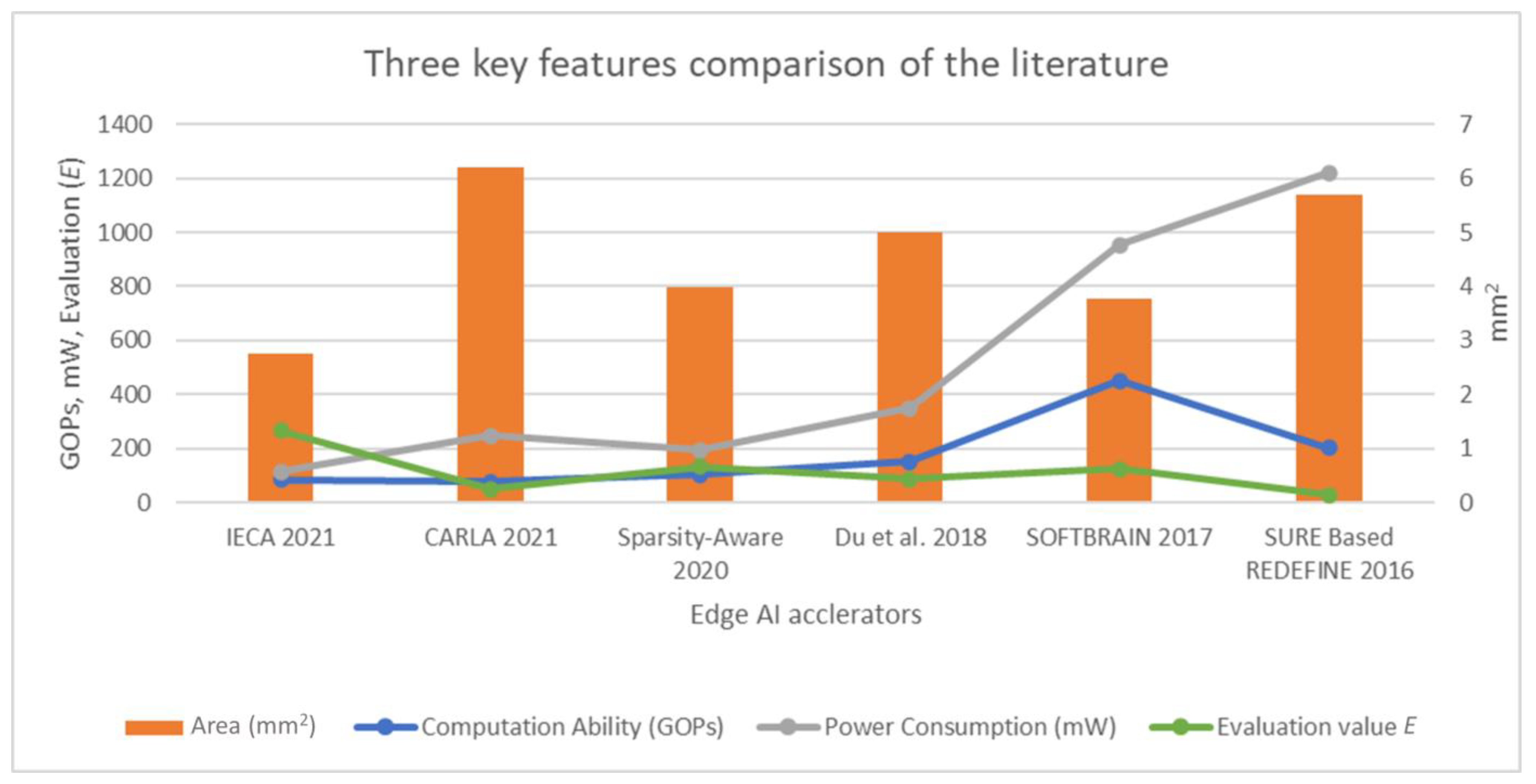
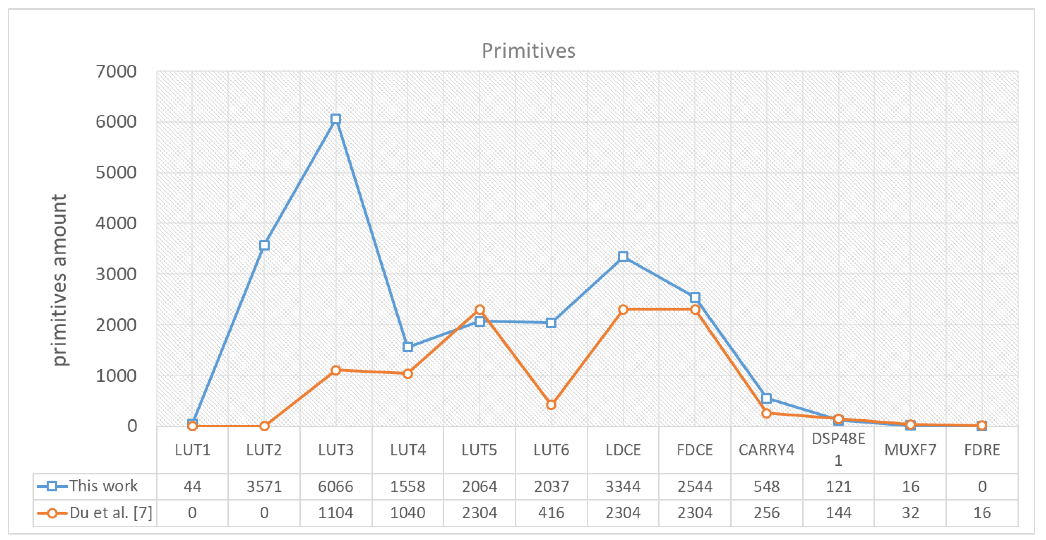
Table 1 introduces the three features: computation ability, power consumption, and the area size of the edge AI accelerators. Although the computation abilities of the accelerators [9,22] are under hundreds of GOPs, they contain relatively lower power consumption. As a result, they are worth to be mentioned in the LPUS edge AI accelerator category in a broad sense. Evaluation value E was introduced by [4] and can be defined as (1). In (1), cFixed16 represents the computation ability of an edge AI accelerator with 16 fixed-point precision, and its unit is Giga operation per second (GOPs). On the other hand, the p and s represent power consumption in W and area size in mm2, respectively.
Evaluation value (E) = cFixed16∕(p × s)
As mentioned, state-of-the-art works [7,8,10,11] fall in the LPUS consumption scope, and three of them [7,8,9] use the streaming/systolic technique, which shows that streaming/systolic architecture in implementing edge AI accelerators proves its efficiency regarding the three features. Furthermore, Du et al. [7] have been commercialized and utilized in a face recognition door lock system powered by batteries; this proves that the streaming dataflow technique is competitive for a convolution engine. Inspired by the streaming approach of [7] and the coarse-grain reconfigurable array design of [8], DycSe is designed to tolerate a certain degree of permanent faults.
To make the comparison in the specifications of the collected edge AI accelerators falling in the LPUS consumption scope clearer, Figure 1 illustrates the three key features with the evaluation E in a line-column chart. Figure 1 shows that [8,10] contain relatively higher power consumption than others, while the design computation of [9,22] is relatively lower. Hence, Sparsity-Aware [11] and Du et al. [7] are the two edge AI accelerators performing more balance in terms of the three key features within the LPUS scope. Furthermore, we also need to be aware that although Sparsity-Aware [11] seems to have the best general performance in the scope, its ASIC design technology is also the smallest, making the general performance better beyond just the architecture design. Since the design in this work targets the convolution engine, which is a component in the whole edge AI system, it is hard to release the three key features in the final ASIC encapsulation form of an IP core. Hence, this work uses a cross-reference [7] to prove that the proposed convolution engine architecture can potentially be integrated into an edge AI accelerator without making the whole system’s performance worse than [7], which has a similar standard with all the arts [7,8,10,11] listed in the scope.

3. Convolution Neural Networks Layers

The convolution function is applied in the convolution layer to calculate the inner product of the input features and weight filters. This process can be understood as mapping the input or previous layer’s features to the next layer according to the emphasized features. At the beginning of the convolution computation, the feature detectors (a set of weight filters) generate the output features of a 2D input image. The output features become the following layer’s input features. Each layer can have multiple input feature channels, such as the RGB color channel, so that the convolution features can be realized as 3D data sets. The convolution output data is obtained by computing the inner product of the filter weight and the part of the input feature masked by the filter.
Figure 2 shows an example of a convolution layer. In Figure 2, k represents a weight filter’s height and width, known as the kernel size. Variable n represents the input layer’s height and width, and m represents the output layer’s height and width. We set a Cartesian coordinate system on the input features to clearly show them. Let O 0 , 0 be the origin, and each input feature’s height and width are n, so point B locates at n , n . At the beginning of the convolution computation, the weight filter’s point ν0,0 is located at O(0,0), so ν0,0 is mapped to 
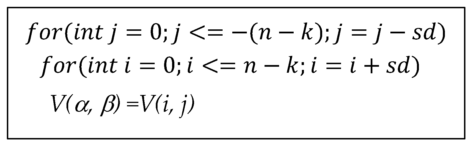
V(α, β), α = β = 0, in the input feature’s coordinate system. Stride sd means the distance that a weight filter would move from the last location V(α, β) to its new location V(α′, β′), which can be realized in Figure 3. When it comes to the output layer, its height and width are m, which can be obtained by (2).
M = ⌊(nk)/sd + 1⌋
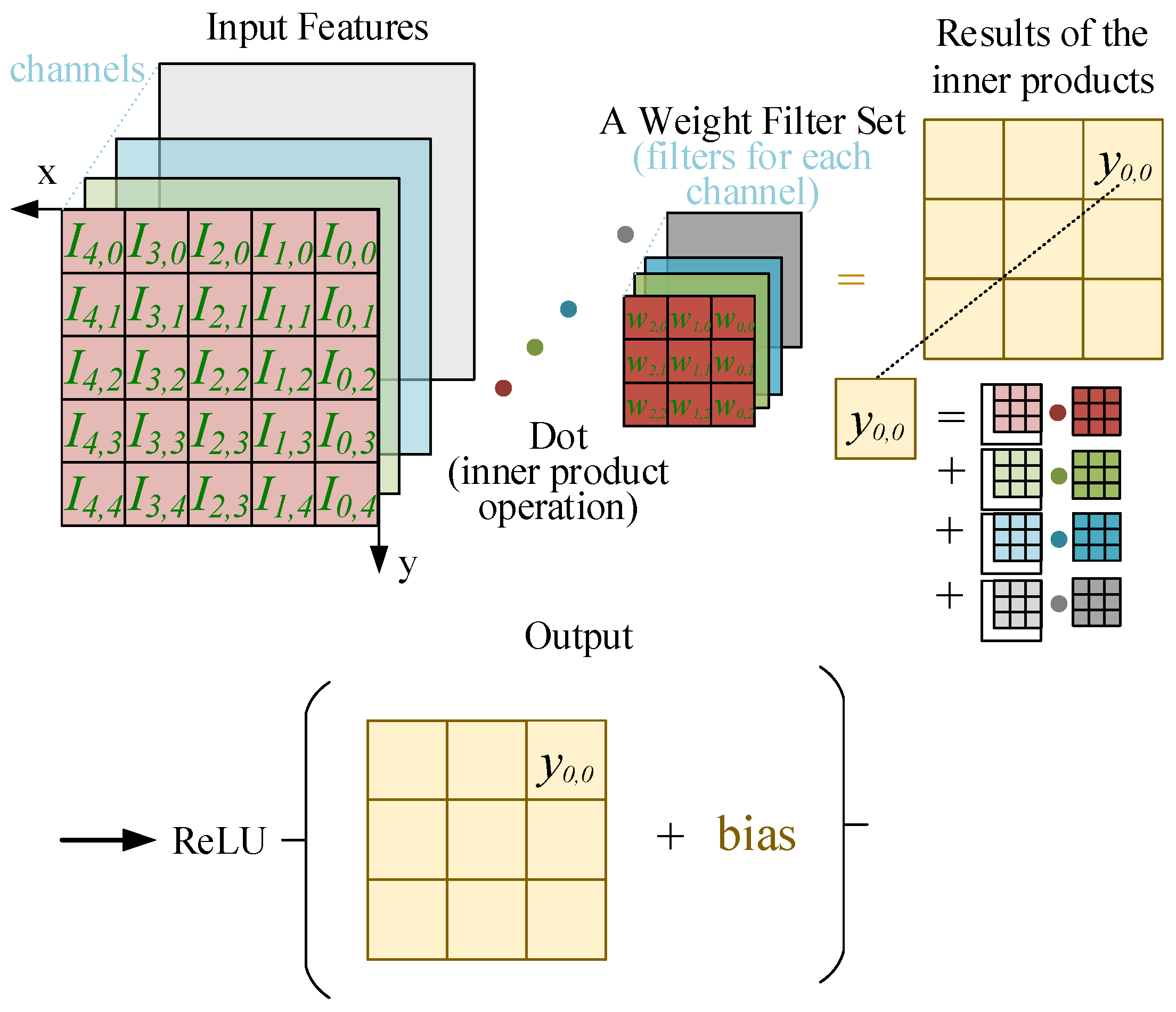
After specifying the variables and their relationships in a convolution layer, we can discuss how a convolution layer can be achieved in computing. The convolution computation of input features and weights obtains an output feature in an output layer. Figure 4 shows the detail of a convolution computation. In Figure 4, we flip the x- and y-axis (x increases to the west; y increases to the south) compared to Figure 3, without the loss of generality. The rest of the paper uses the reversed axes system to represent the convolution computation.
Convolution computation can be seen as a filter scanning through an input layer according to the stride size to generate and direct the result to an activation function with an extra bias. The overlapping input feature’s pixel and weights in the weight filter during the scanning should do the inner product, as shown in Figure 4. Each output feature is obtained by summating the inner products produced by each input feature and weight filter. After the sum is received, an additional bias weight is added to each summed result, followed by applying the final result to an activation function ReLU.

4. Column Streaming-Based Mapping Algorithm

According to our investigation and [23], several kinds of reconfigurable strategies are used in these state-of-the-art accelerators [7,8,11,24,25]. Among these accelerators, the reconfiguration of [7,11] is limited to dataflow, while Jiao et al. [24] and Ryu et al. [25] target word size type reconfiguration. SOFTBRAIN [8] utilized a coarse-grained cell array to compute the stream-dataflow DNN. Except for [7,11,24,25], only SOFTBRAIN [8] falls into components or module reconfiguration (i.e., structure-wise reconfiguration). Du et al. [7] and SOFTBRAIN [8] adopt the competitive streaming architecture, as in Table 1 and Figure 1.
Hence, streaming architecture is chosen for DycSe to provide a convolution engine for edge AI accelerators. An edge AI accelerator requires processing AI algorithms (i.e., CNN in this paper). Since CNN algorithm is a general term for different CNN nets, which contain many different convolution layers, a convolution engine in an edge AI accelerator with the ability to adapt arbitrary weight filters is becoming essential. Structure-wise reconfiguration is proposed to offer the ability to process arbitrary weight filter size and the fault tolerance requirement (i.e., condition IV in chapter 1). Structure-wise reconfiguration includes hardware rearrangement through programmable connections, such as muxes or demuxes. Hence, it differs from a dataflow-wise reconfiguration such as the weight filter decomposition technique proposed by [7]. The detail of the structure-wise reconfiguration is described in chapter 5.
Before designing a convolution engine structure, a hardware mapping algorithm should be created first, deciding the structure’s developing flexibility. Hence, a proper mapping algorithm for weight filters and input features to be mapped to the convolution engine architecture is discussed in this chapter. Section 4.1 introduces the strategy, while Section 4.2 examines the concept. Finally, Section 4.3 releases all the mapping varieties categorized by mapping methods, which are represented by the notation method, equal to 1 or 2.

4.1. Convolution Computation Mapping Strategy

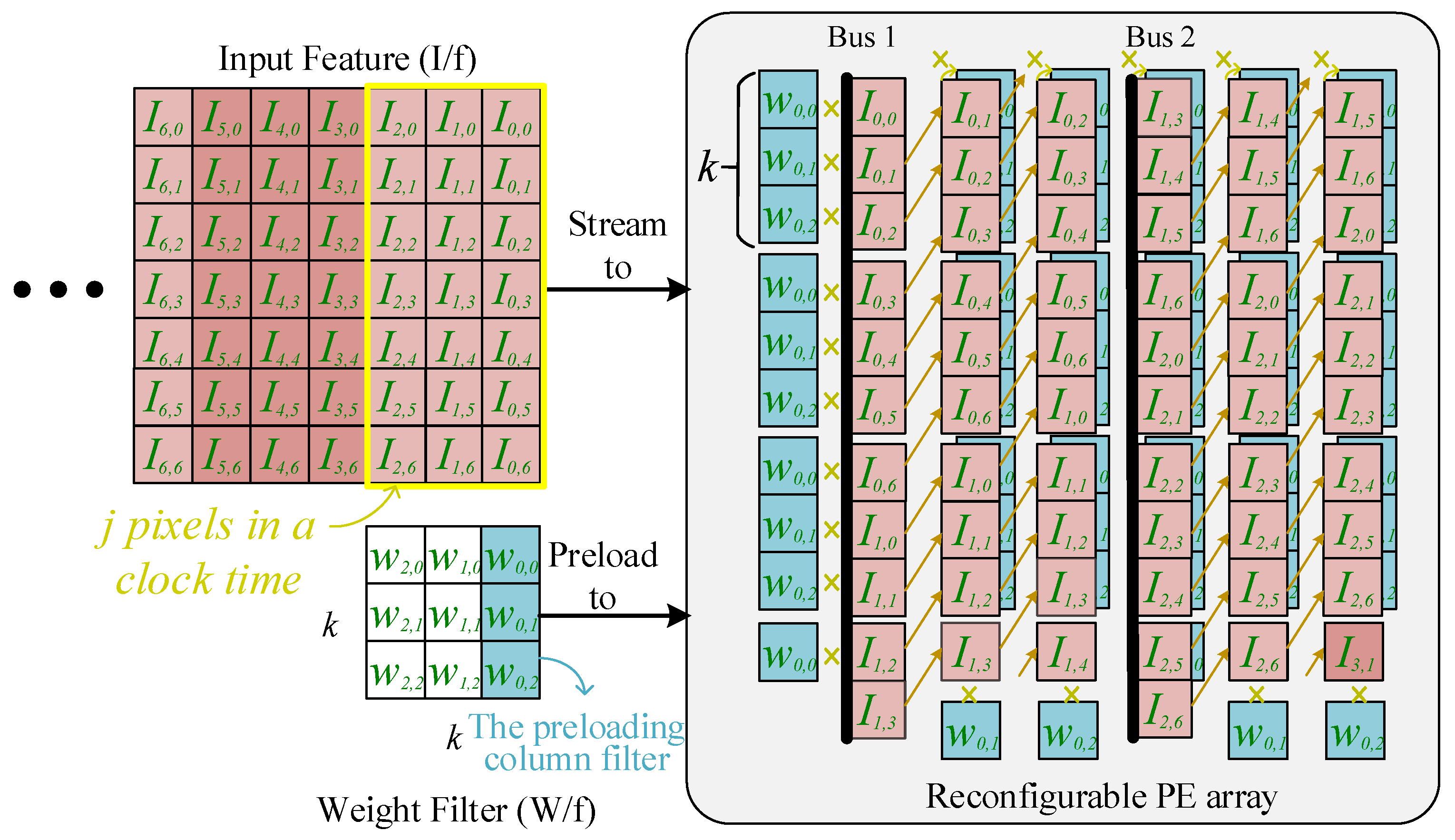
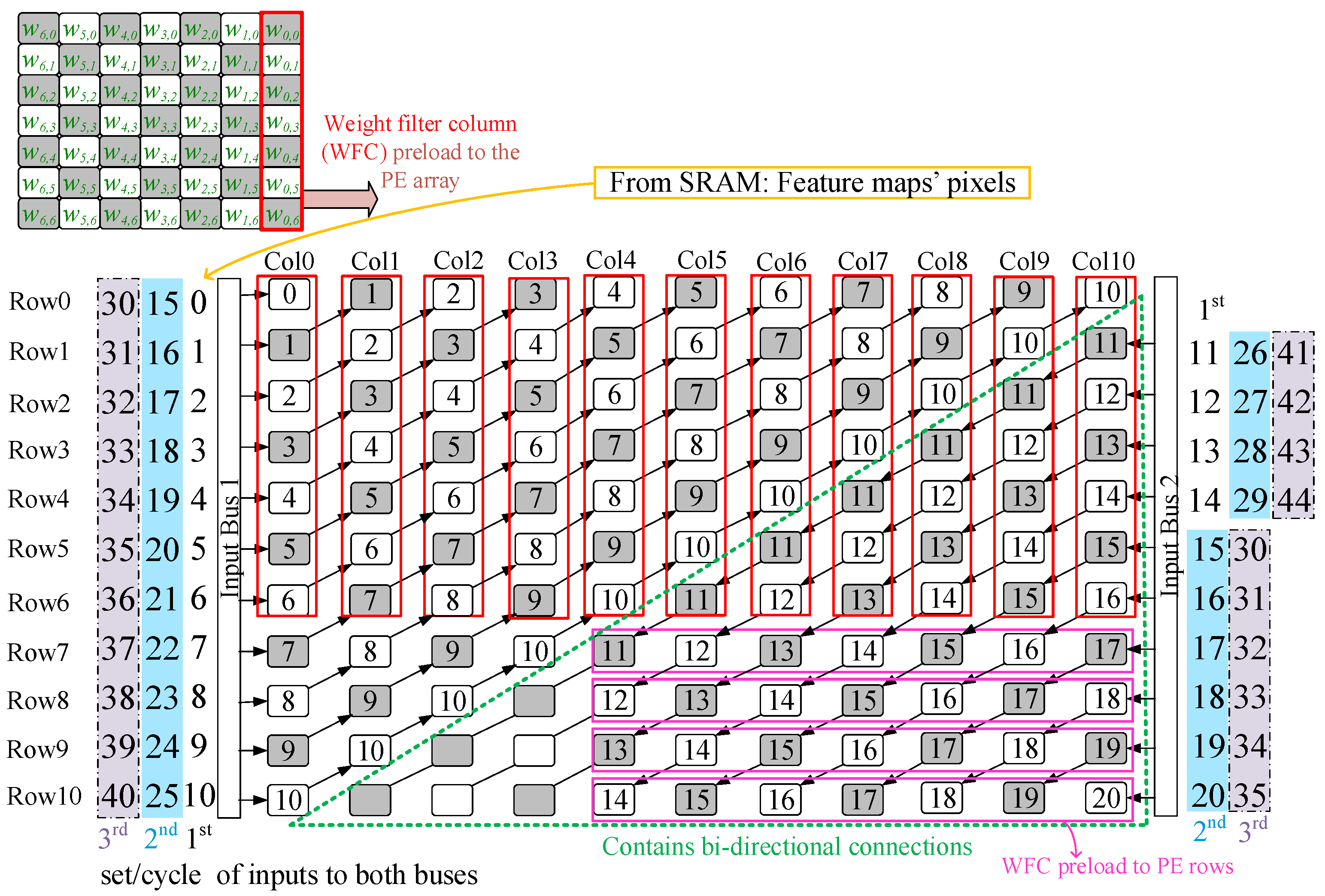
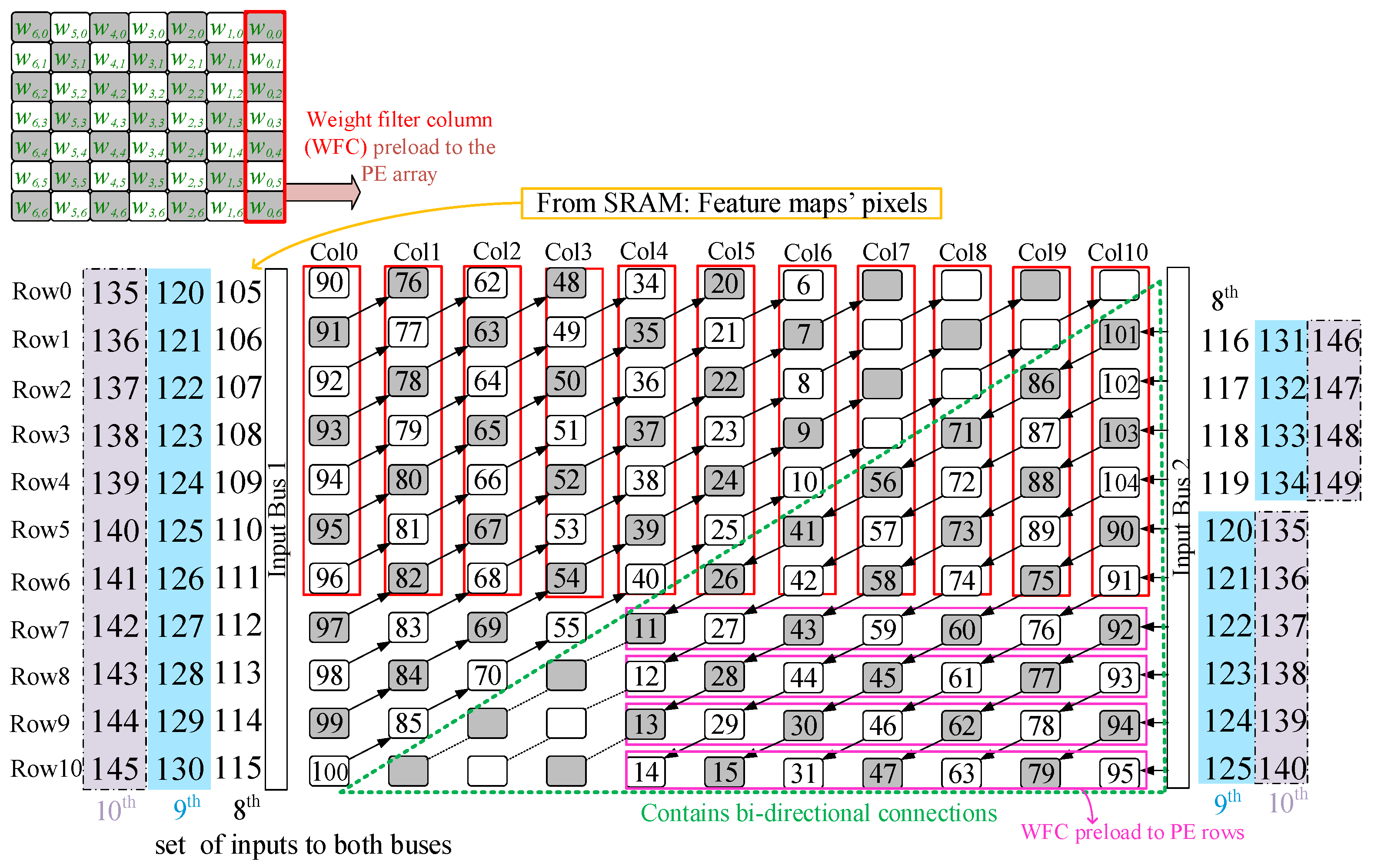
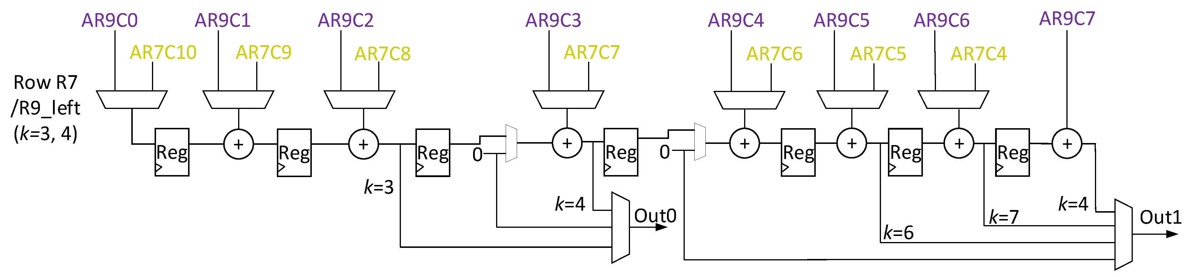
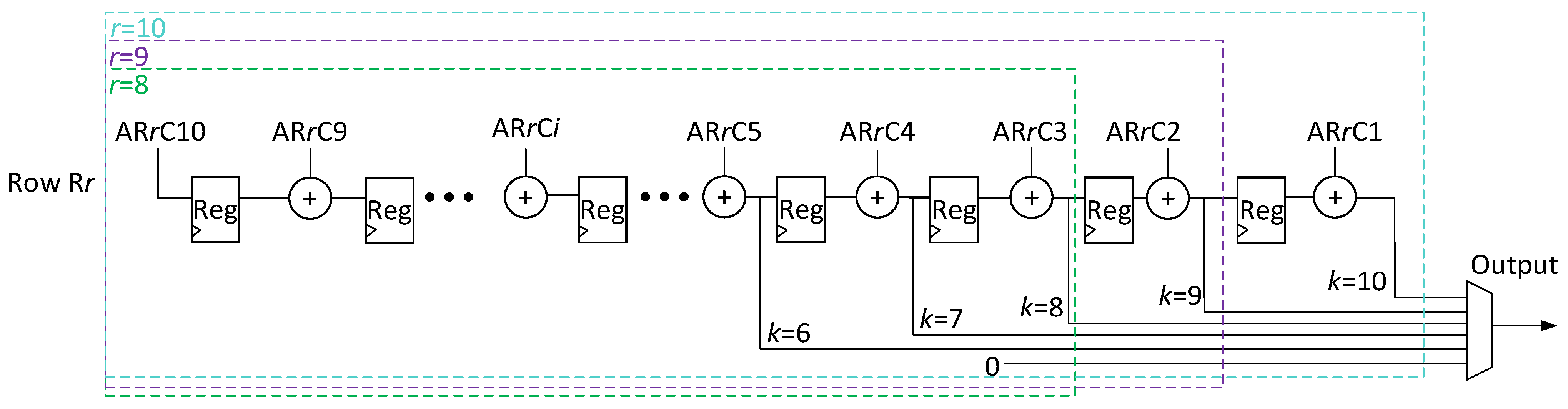
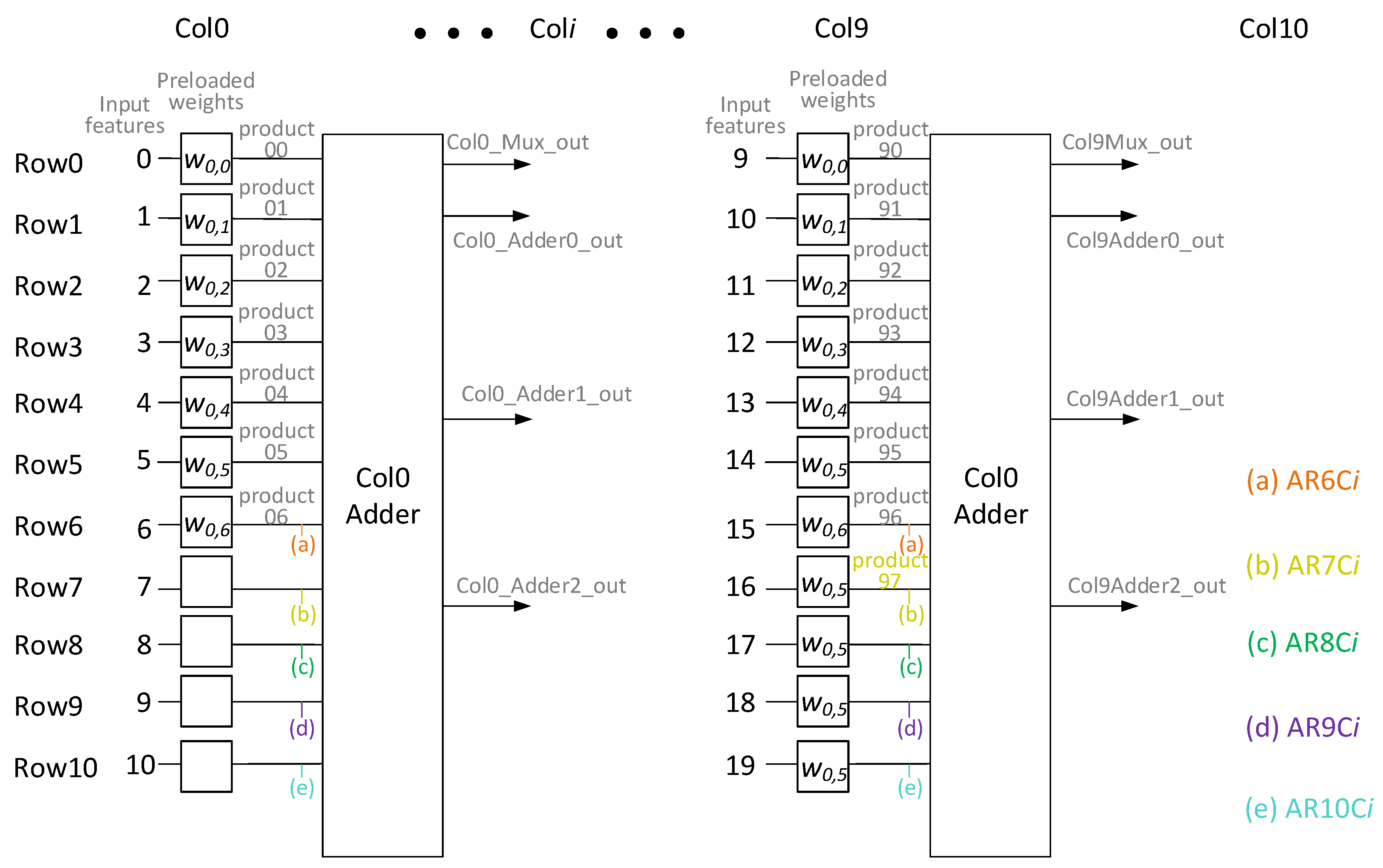
Figure 5 shows DycSe’s data mapping strategy for convolution computation, achieved by the column streaming methods. Figure 5 is composed of three blocks, input features (I/f), weight filters (W/f), and the PE array (module), where the convolution computation executes; the weight values in the W/f block preload to the PE array in column form. The filter size decides the weight-mapped position and how the PE module is configured.
A k × k-sized W/f is decomposed into k columns. When k = 3 in Figure 5’s case, the first column, {w0,0, w0,1, w0,2} in blue, preloads into the array, and the weight column stays in the PE array until the input feature data finishes the multiplication.
The input feature is decomposed into j data (pixel) sets, and a data set is steamed into the PE array at each clock cycle. The variable j is also decided by the mapping method that, according to the PE module reconfiguration, 𝑗 in Figure 5 is 21. The 21 inputs of data are streamed into the PE array in two subsets, through Bus1 and Bus2. Variable j can be obtained by using (3). In (3), variable k represents the kernel size, variable c represents the streaming data set, and variable method represents the mapping methods. Variable AH means PE array heights.
j k , c , m = A H × 2 1 ,     k 5 ,   c = 0 ,   m e t h o d = 1 j k , c , m = A H × 2 2 ,     k 5 ,   c > 0 ,   m e t h o d = 1 j k , c , m = A H × 2 k ,     k 5 ,   c 0 ,   m e t h o d = 2   j k , c , 2 = A H × 2 1 k ,     k > 5 ,   c 0 ,   m e t h o d 2

4.2. Mapping Strategy Comparison

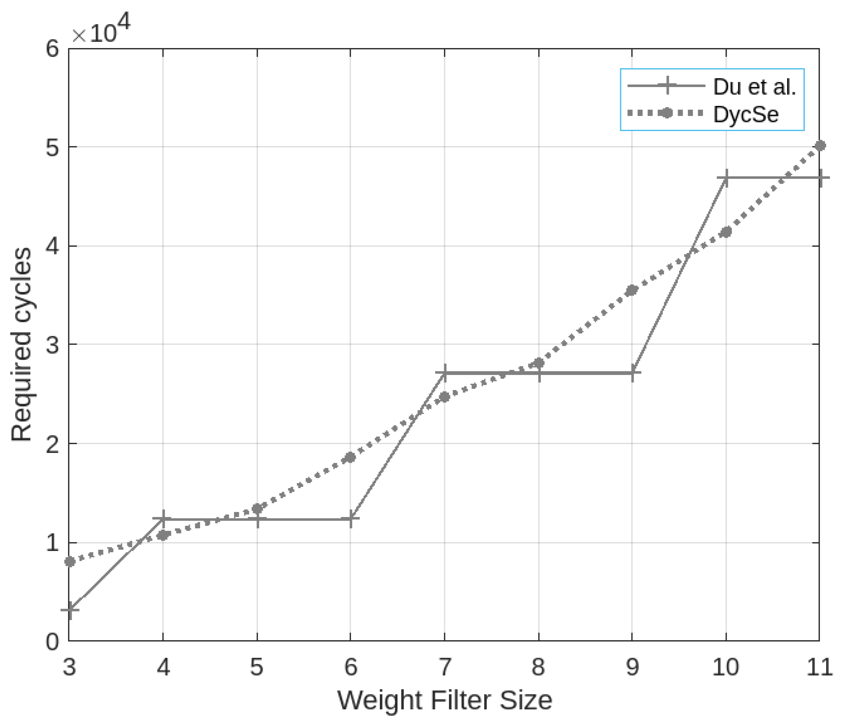
For evaluating the column streaming-based convolution engine, we use MATLAB to count the execution cycles needed for DycSe and [7] to compute a 227 × 227 size feature map in the pilot study [5]. A 227 × 227 size feature map is the input size of AlexNet, one of the famous CNN.
As shown in Figure 6, the calculation result shows that the proposed convolution engine requires fewer cycles to compute the feature map when the weight filter size is equal to four, seven, and 10. When the weight filter size equals five and eight, the proposed convolution engine shares similar execution cycles. The proposed convolution engine needs more cycles to compute the operations when the weight filter size equals three, six, nine, and 11. Figure 6 shows that the dash line, indicating the result of the algorithm adopted by DycSe, goes through the solid line Du et al. [7]. The dash line looks like the regression line of the solid line because the column streaming algorithm [5] tries to avoid the zero-padding boundary penalty of [7].
After the LPUS scope has been decided, an efficient convolution engine structure is expected to be proposed by following the LPUS scope’s standard. The dataflow oriental structure is the DycSe’s core design idea, indicating that the input data, such as I/f and W/f, demand an algorithm to be mapped on the hardware. Since Du et al. [7] share similar performance in the three key features within the LPUS scope accelerators, retaining the data processing cycles not worse than [7] is the goal, making DycSe stand at the same level as the other architectures in the scope.
The column streaming algorithm [5] tries to eliminate the zero-padding [7] to reduce the cycles, which are only for passing through the data but are not used for computing the multiplication under specific filter sizes. The filter sizes require zero-paddings, which do not equal a multiple of three. When zero-padding is used, although the multiplier in the unused PE is turned off to avoid power consumption, the flip-flop in the PE is still working for streaming the data. The result also indicates that the worst penalties happen at the filter size, which equals 3 k + 1 ,   { k | k + a n d   1 k < 4 } , which can be observed in Figure 6.

4.3. Mapping Methods and Varieties for Flexibility

This section introduces the input feature and weight mapping strategy according to the different mapping varieties. In this section, there are two mapping methods (i.e., method = 1 and 2) introduced. Mapping method = 1 contains several mapping varieties, while method = 2 only has one. In Section 4.3.1, we present how the input feature is streamed into the PE array and defines the Bus’s location. According to the input feature’s mapped location in the PE, Section 4.3.2 introduces the preloaded weight’s mapping destinations.

4.3.1. Input Feature Mapping

Providing different mapping varieties (v) for particular-sized filters is the featured function of the proposed convolution engine. The mapping varieties (v) of filter size (k × k), 3 k 11 ,   and   k 0 can be found in (4). Each mapping variety is equivalent and can be regarded as each other’s substitution when some PEs fail. The upper bound of k in a w × h PE array is h (in this paper, w = 11, h = 11), but the array can be flexibly enlarged and customized. Table 2 lists all the possible mapping varieties and compares them to [7].
v   for   filter   size   k 2 ,   i f   k w 2 h = 1 ,   i f   w 2 < k h
According to the Bus2 location, we define two mapping methods, 
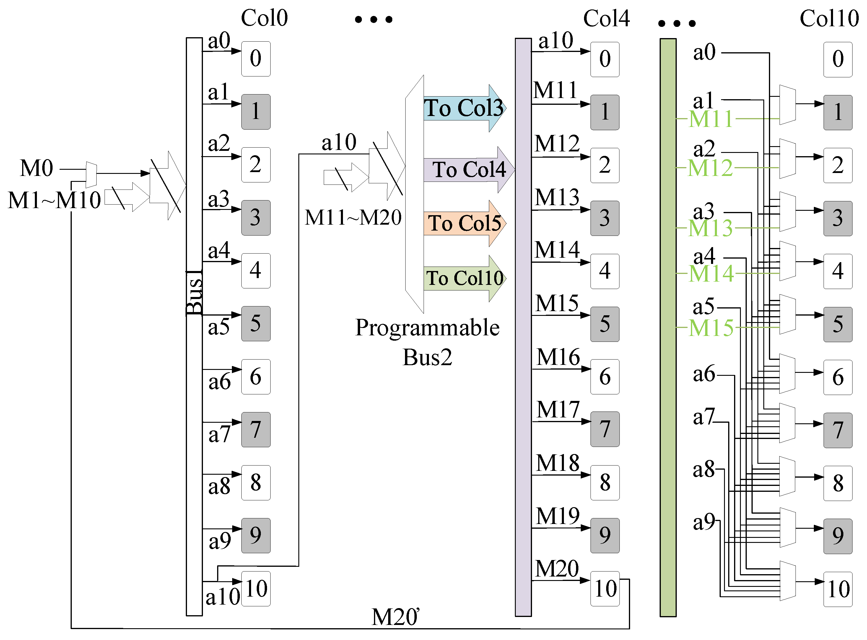
method = 1 and 2. When method = 1, Bus2 can locate at Coli ( k i w 2 ), by default i = k . Mapping method = 1 can only be adopted when the filter k w 2 . Different from the case, method = 1, generally for k > w 2 , the case method = 2 is also available for k w 2 when providing the PE array flexibility and reliability. Bus2 streams data to the rightest column, Col(w − 1), when in 
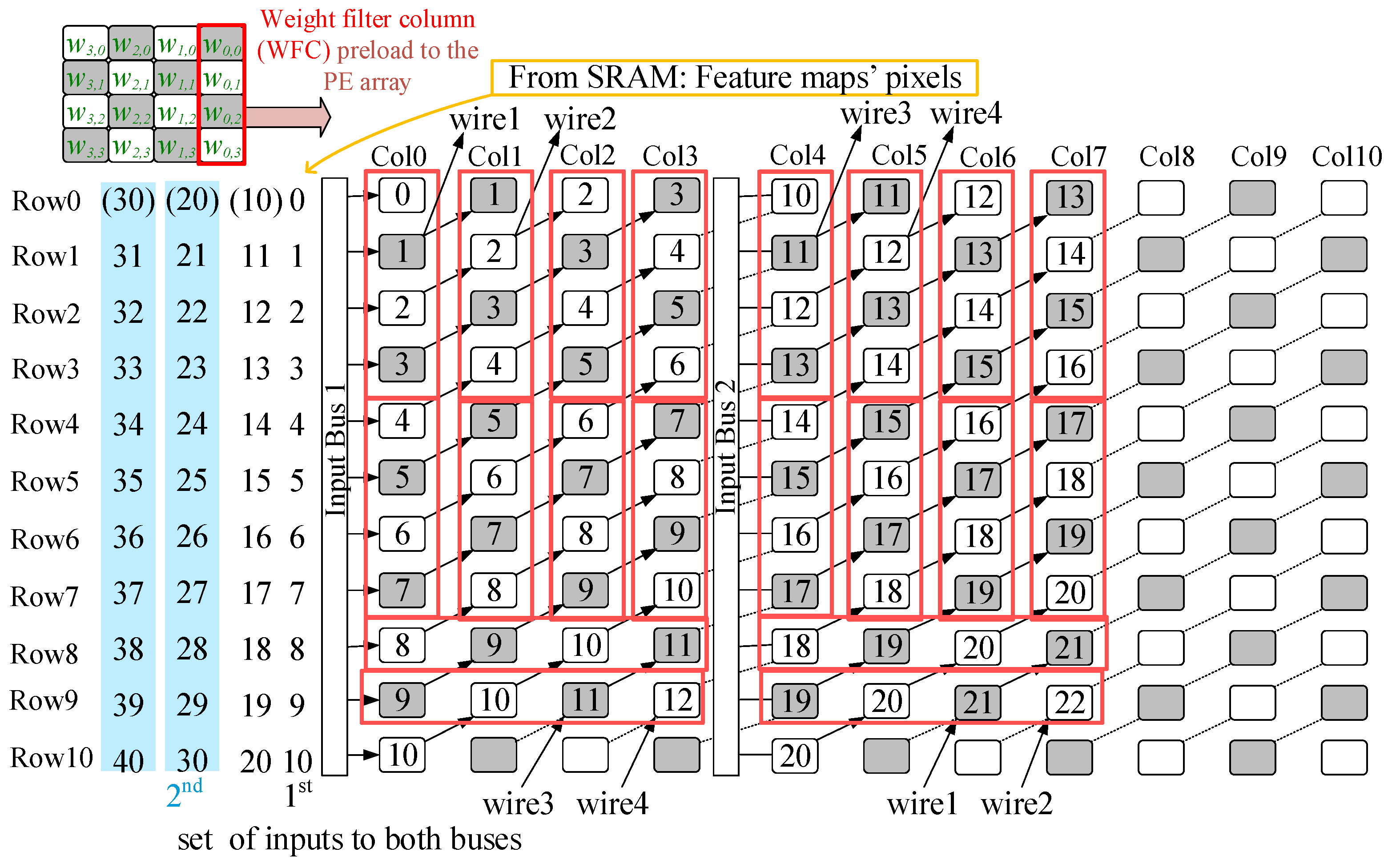
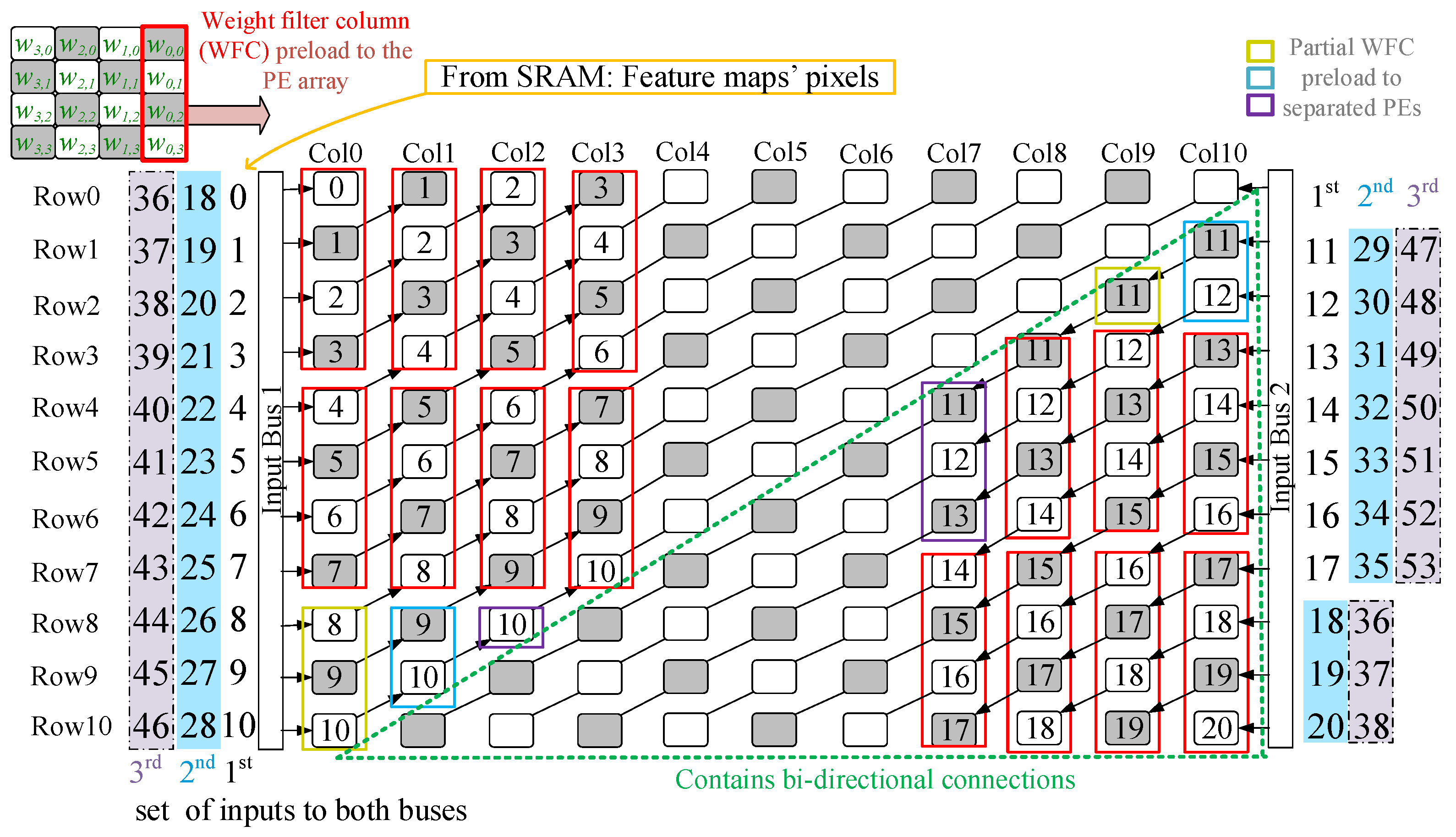
method = 2. For example, 
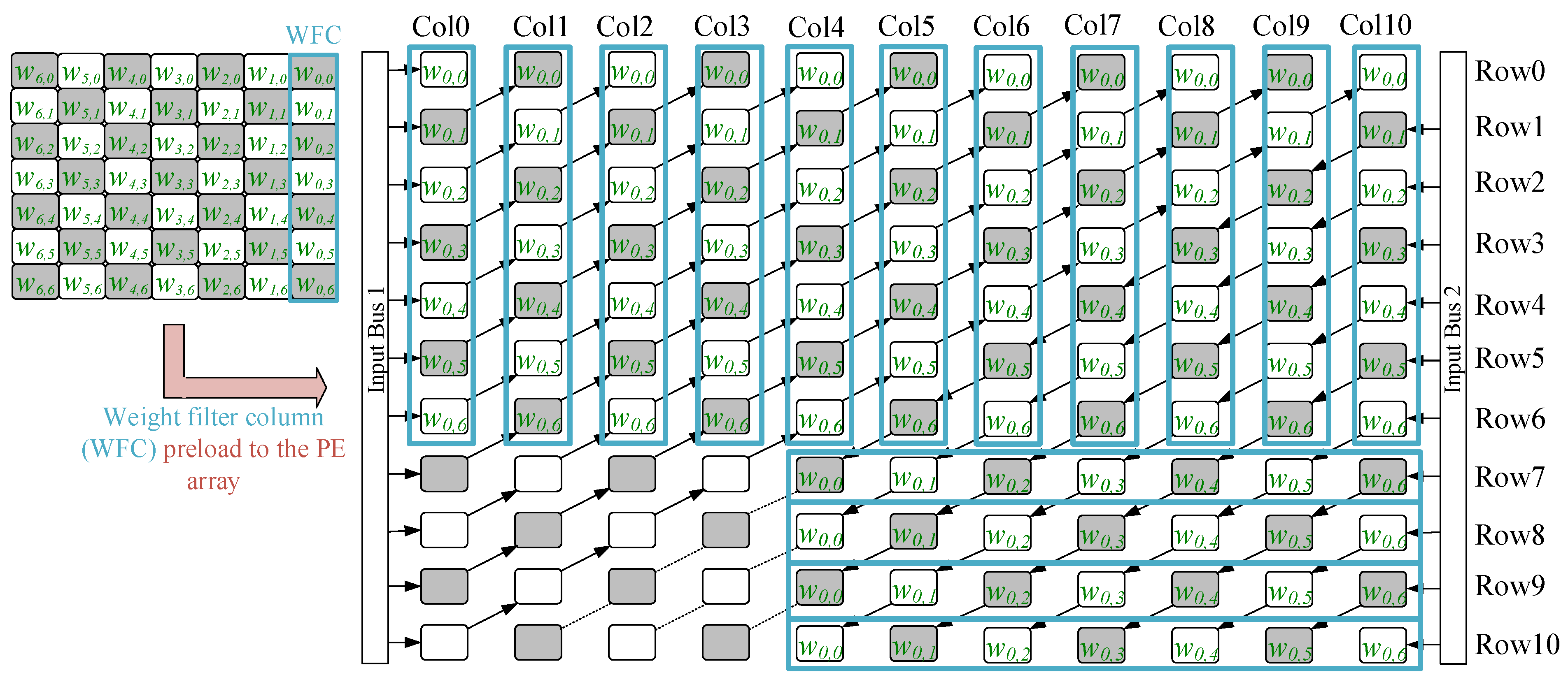
Figure 7 shows a 4 × 4-sized filter method = 1, and Bus2 streams the data into Col4 (i = 4). Bus2 can also pour data into Col5 (i = 5) when a 4 × 4-sized filter uses the other mapping variety with method = 1. On the other hand, Figure 8 shows a 4 × 4-sized filter method = 2, and Bus2 streams data into Col10 (i = 10). The data from Coli, i = 10, is streamed to Colj (0 < j < 10) cycle by cycle. Overall, there are three mapping varieties (two types when method = 1 and 1 type when method = 2) for a 4 × 4-sized filter.
In the k > w 2 cases, the mapping method is limited to one variety, method = 2, as shown in (4). Figure 9 and Figure 10 show the case a 7 × 7-sized filter case. Since the k in the case is 7 and is bigger than w 2 so that method = 2 is adopted. Table 2 concludes the mapping varieties for the filters 3 × 3 to 11 × 11, indicating that one-third of the filters contain at least two mapping methods to provide flexibility. For increasing the flexibility and providing more mapping methods for the filters k > w 2 , the array can be flexibly enlarged and customized to increase w and h.

4.3.2. Weight Mapping

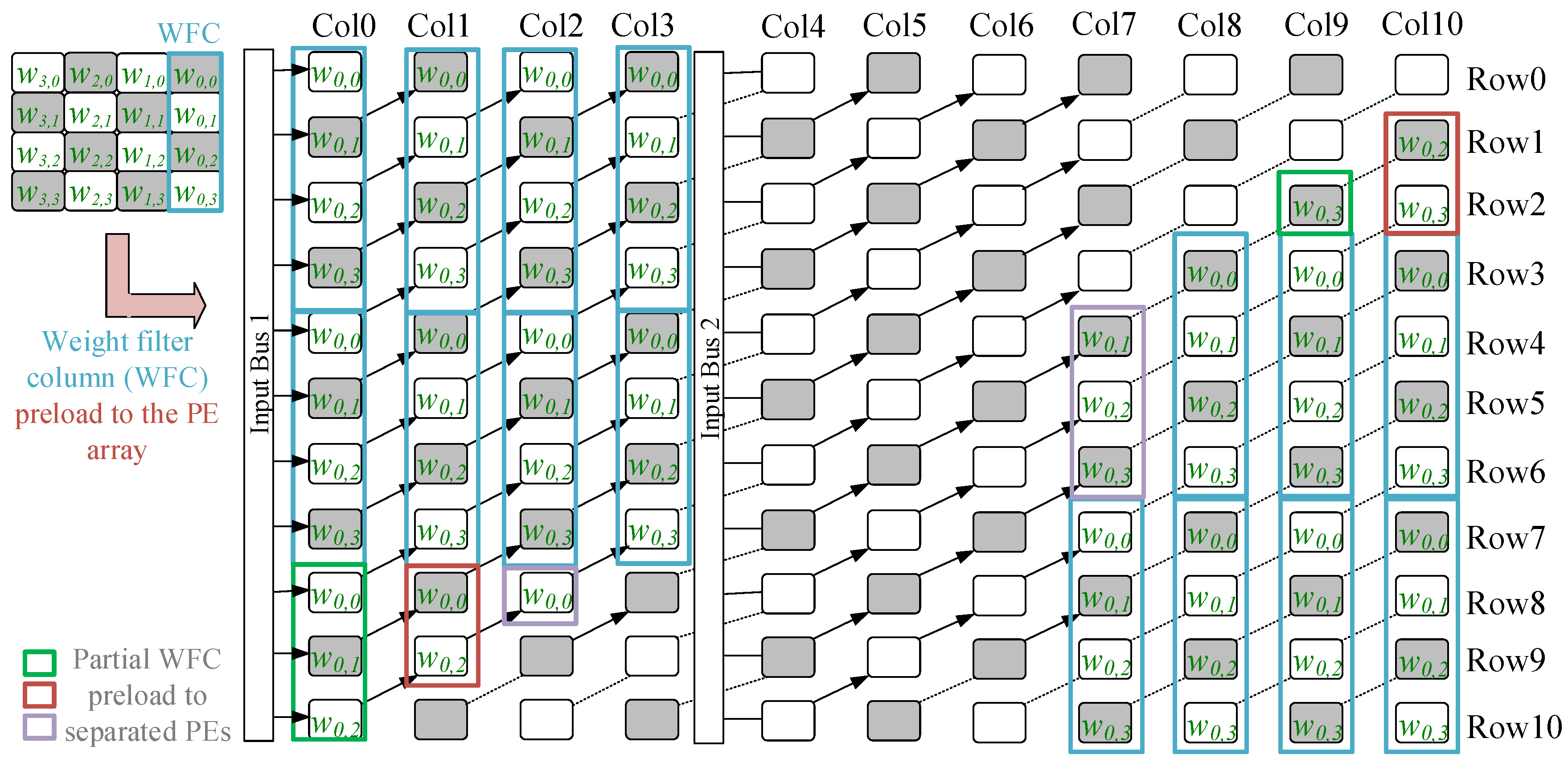
Weight mapping varieties follow the mapping varieties of input features. Bus2 is set to a different position in different mapping varieties to let the input features stream into the PE array. Before streaming, the weights are preloaded to the array according to the required variety. The following examples show the weight mapping location when using the 4 × 4-sized and 7 × 7-sized filters with method = 1 and 2.
Figure 11 and Figure 12 illustrate the weight filters map to the required location according to the different mapping varieties. Without loss of generality, Figure 11 uses a 4 × 4-sized filter to show the mapping method, method = 1 (Coli = Col4), while Figure 12 uses a 7 × 7-sized filter to demonstrate the mapping method, method = 2. In Figure 11, the 4 × 4-sized filters preload their first column, circled by the blue squire, to the PE array. Hence, the first column {w0,0, w0,1, w0,2, w0,3} loads to the required positions and waits for streaming input feature data. Then, the multiplication action happens in the circled PEs shown in Figure 7. On the other hand, Figure 12 shows the mapping method, method = 2, using a 7 × 7-sized filter as an example. Figure 13 shows the other case, k w 2 , of using mapping method, method = 2, for the flexible purpose of utilizing a 4 × 4-sized filter as an example.

5. Column Streaming-Based Convolution Engine Architecture

This section introduces the hardware structures that implement the mapping algorithm [5]. The hardware structures comprise several modules, processing elements (PE), programmable Bus2, and an adder module. Unlike prior trial work [6] that only implements a small PE array for primary evaluation, the work in this section contains a full-size convolution engine structure.
The detail of the structure is organized below. Section 5.1 introduces PEs with connections, including the bi-directional design. The programmable Bus and connection for data reusing are explained in Section 5.2. Finally, the adder module is shown in Section 5.3.

5.1. Processing Elements and Their Connections

Each PE comprises a D flip-flop-based register and a multiplier, as shown in Figure 14a. The data width of the components and connections are set to be 16-bits fixed as the trend of the edge AI accelerators [7,9,11,13,14,22], already proving that DNN can be represented with 16-bit fixed-point numbers with fewer logic gates.
The PEs shown in the green dashed lines in the above data mapping figures, such as Figure 9, are designed to be bi-directional. For selecting the input data from the required direction, a two-to-one multiplexer (mux) is added ahead of the input of the D flip-flop in the bi-directional PEs. Figure 14b shows how the bi-directional PEs broadcast their output to the two adjacent PEs by programming wire selection. If a PE’s location locates at column x and row y, it can be represented as PE(Colx, Rowy), { 0 x 10 ,   0 y 10 ,   and   x , y 0 } . The coordination system can be found in Figure 7, Figure 8, Figure 9, Figure 10, Figure 11, Figure 12 and Figure 13. PE_outL represents the data that comes from the left side PE( Col x 1 ,   Row y + 1 ) output. For example, in Figure 7, the PE(Col6, Row5) is programmed in the left-to-right direction and accepts the input from PE(Col5, Row6).
On the other hand, the bi-directional PEs are programmed to accept data from PE_outR coming out of PE(Col(x + 1), Row(y − 1)) when the method equals 2. For example, PE(Col6, Row5) is programmed to propagate data from the right-to-left direction and stream the data to PE(Col5, Row6) when accepting the input from PE(Col7, Row4), as shown in Figure 9. If a PE does not need a bi-directional connection but only left-to-right propagation (from Colx to Coly { 0 x < y 10 ,   and   x , y 0 } ), the mux in front of the PE input is removed to save the FPGA resource.

5.2. Programmable Bus and Its Connection

A flexible programmable bus structure is proposed, connecting to the PEs to form a column streaming array. Bus2 is designed with the demultiplexers (demuxes) for being programmed to stream the input data to the required column, as shown in Figure 15. Depending on the mapping methods and varieties, the selected demux output can be Col3, Col4, Col5, or Col10. The details of the demuxes set up in the programmable Bus2 can be observed in Figure 16.
Regarding data reusing, the connections in programmable buses have been designed to reduce repeated external memory accessing, such as SRAM out of DycSe, and maximize data reusing, such as a10 and M20’ in Figure 15. For example, a10 is utilized in Figure 7’s case, and two data subsets {20i, 20i + 1,…, 20i + 10)} and {20i + 10, 20i + 11,…, 20i + 20} are streaming the same data ‘20i + 10’ (e.g., data ‘10’ in the first set) to Bus1 and Bus2, {i|0 i ,   i 0 } . Wire M20’ is another example of data reusing in Figure 15. The ith and (i + 1)th data set are {20i, 20i + 1,…, 20i + 20} and {20(i + 1), 20(i + 1) + 1,…, 20(i + 1) + 20}, respectively. The data 20i + 20 and 20(i + 1) are duplicated and appear in both data sets, such as data ‘20’ in the first and second sets.

5.3. Reconfiguration Adder Module

The adder module should be able to handle multiplication products generated by different PE groups, whose result requires adding up according to the algorithm. As shown in Section 4.3, different mapping varieties make each group of multiplications happen at the different PEs groups (e.g., Figure 7’s PEs in the red rectangles), which generates a partial sum. If the products of a group of PEs are added together, we call this group a partial sum group. The examples can be observed in Figure 7, Figure 8, Figure 9 and Figure 10, and their partial sum group can be grouped vertically or horizontally.
To identify partial sum groups, we defined a notation system (5)–(8) to represent how the partial sum was obtained from different PEs. If the partial sum means to generate vertically, the partial sum group can be defined as Psum { PE ( Col x , Row y ~ Row y + k 1 } , of which the definition is shown in (6). If the partial sum generates horizontally, the partial sum group can be represented as Psum { PE ( Col x ~ Col x + k 1 ,   Row y } , defined in (7).
Psum { PE Col x , Row y ,   PE Col x , Row y ) } = PE Col x , Row y + + PE Col x , Row y
Psum { PE ( Col x , Row y ~ Row y + k 1 } = i = 0 k 1 Product   generated   by   PE Col x , Row y + i
Psum { PE ( Col x ~ Col x + k 1 , Row y } = i = 0 k 1 Product   generated   by   PE Col x + i , Row y
Psum Psum , , PE Col x , Rowy = Psum + + PE ( Col x , Row y )
The other partial sum group cases are the multiplication input data mapped to nonadjacent PEs. As shown in Figure 8, Psum{PE(Col0,Col8-9), PE(Col9, Row2)} are generated by the PEs(Col0, Row8~Row10), containing the output data {8·w00,9·w01,10·w02}, and the PE(Col9, Row2), containing data {11·w02}. To easily present the partial sum groups composed of nonadjacent PEs, the same color of rectangles is used, such as in Figure 8, to indicate the same partial group.
For implementing the different summation demands, the adder module is designed to have the ability to add up the multiplication products vertically and horizontally. The adder module comprises two submodules: a column and a row adder submodule.
The column adder submodule is shown in Figure 17, which is used to handle the vertical products adding up cases according to different filter sizes k, Psum { PE ( Col x , Row y ~ Row y + k 1 } . There are 11 columns of adders in the column adder submodule. Each column in the column adder submodule consists of three seven-input adders and a set of programmable components, such as demuxes and muxes, responsible for remapping the result from the PE array. Each sub-column adder module generates the partial sum and sends the result to the accumulator module.
On the other hand, partial sums from the PEs are required to be added horizontally. However, the horizontally adjacent PEs stream the input data in the different clock cycles. There is a cycle delay in some cases, such as between PE(Col4, Row7) and PE(Col5, Row7). As a result, the column adder module requires delay buffers to adjust the addition operation timing. The delay chain design in the row adder module can be observed in Figure 18 and Figure 19.
There is a total of five adder rows in the row adder submodule. When k = 3, the seventh row of the adder (row R7) shown in Figure 18 is utilized. When k = 4, the sixth and seventh rows of the adder (rows R6 and R7) shown in Figure 19 are utilized. The other name of adder row R7 is R9_left, which indicates that when k = 3 and 4, in the PE array’s point of view, R7 is their row 9 and uses the left inputs AR9Ci in Figure 7, Figure 17 and Figure 19. In the same way, the other name of adder row R6 is R8_left, which means it is also utilized by PE array row 8 in the k = 4 case. In Figure 7, the four partial sum groups, Psum{PE(Col0~3, Row8)}, Psum{PE(Col0~3, Row9)}, Psum{PE(Col4~7, Row8)}, and Psum{PE(Col4~7, Row8)}, are required to be added up horizontally. Hence, in this case, R8_left and R9_left are used.
Row adders R8~10 are shown in Figure 20, which are utilized by the cases of k = 6~10. Figure 20 is a condensed version of all three adder rows R8~10, which uses the dash line rectangles to represent the three different adder rows’ structure, r = 8~10. The input amount of the output mux in the figure is a variable according to how many wires are circled by the individual dash line rectangle. For example, there is a five-to-one mux utilized when r = 9. Figure 9 is an example of k = 7. In the example, it can be noticed that there are four partial sum groups, rows 7~10, required to be added. To implement the Psum{ PE ( Col 4 ~ Col 10 ,   Row y }, y = 7~10, adder row R7~10 is utilized.

6. System Verification and Experiment Results

This section summarizes the hardware verifications and simulation results by using the Xilinx Vivado high-level synthesis tool. This section is divided into two subsections: structure verification and synthesis results. In the structure verification subsection, we preload the weights into DycSe, and the weight mapping method is according to the weight filter size. Then, we stream the input data to the PE array and collect the partial sum results from the output of the adder module to verify the structural correctness. The experiment results are shown in the subsections containing the synthesis result comparisons between DycSe and Du et al. [7], since it has proven its advantage in the LPUS scope. The result lets DycSe show its potential to be integrated into the edge AI accelerators to increase flexibility without using too many resources.

6.1. System Verification

We load the testing data to the buses to verify the convolution engine and extract the output from the adder module. Due to the limitation of the pages, we only show a few testing data, which may not comprehensively represent the whole convolution engine, but it does not lose the generality. Figure 21 shows how the data is imported to Bus1 and streamed to other PEs. First, the weights are preloaded to the PE array, and in this case, the weights {w0,0, w0,1, w0,2, w0,3} are {weight00, weight01, weight02, weight03} in Figure 21, which equal to {1, 0, −1, 1}. We extract four sets of data as an example to show the waveform. The data that comes into Bus1 are Bus1_in0, Bus1_in1, Bus1_in2, and Bus1_in3, which multiply the weights and generate the products. The products are product00, product01, product02, and product03. As shown in Section 4.3.1, the PE(Col0, Row0), accepting the data from BUS1_in0, streams the data to PE(Col1, Row0) and PE10_in in Figure 20, in the next clock cycle.
For verifying the adders, the filter cases k = 7 are used as an example, which contain the utilization of both column adder and row adder. Figure 22 and Figure 23 show the column adder Col0 and Col9’s operations for summing up the products from the PE array. All the data signals in Figure 22 and Figure 23 are illustrated in the schematic view in Figure 24.
Figure 9 shows that rows 7~10 in the PE array are also used to map the input features and weights. To present the signals in the row adder module, we use PE array row 7 as an example. The example uses the row adder, R7, to summarize the products. In Figure 25, the signals, product47, product57, product67, product77, product87, product97, and product107, are the products generated by the PE(Col4, Row7), PE(Col5, Row7), PE(Col6, Row7), PE(Col7, Row7), PE(Col8, Row7), PE(Col9, Row7), and PE(Col10, Row7), respectively. The signal product97 locates at Col9 wire (b) in Figure 24 and is redirected to wire AR7C9 in Figure 19. Similarly, all the other products, such as product47, product57, product67, product77, product87, and product107, are also redirected to R7 for generating the partial sum.
It is worth mentioning that the test data are created on our own to verify the structure. The testing data are 16 binary bits for input features and weights. In future work, the testing will use actual picture pixel data and pre-trained weights for performance specification collection.

6.2. Experiment Results

To evaluate the benefit of the trade-off between the flexibility provided and the resource used by DycSe, we implement the convolution engine structures of both DycSe and [7] on the Xilinx Vivado synthesis tool. Both structures contain a PE array, an adder module, registers, and programmable connections. Since under similar processing cycles, the PE amount used in DycSe was 121, and the PE amount of [7] requires 144, this indicates that the column streaming mapping algorithm for the PE array can reduce the PE amount by eliminating the paddings [5]. Hence, DycSe gains the spare resources for the reconfigurable connections in terms of flexibility.
To move forward and form the full-size multiply-Add (MAD) modules in a complete convolution engine, an adder module is also integrated into DycSe and [7] for a fair comparison. The convolution engine implementation result of DycSe and [7] is released in this subsection. By a cross-reference from [7], we can see the DycSe’s potential for integrating into a complete system of an edge AI accelerator in terms of LPUS scope.
Table 3 releases the primitive usages consumed by DycSe and [7] when choosing Virtex-7 XC7VX485T as the targeting product. To clearly show the comparison, we direct the data in Table 3 to a line chart, shown in Figure 26. In the line chart, the blue line illustrates the primitives used by DycSe, while the orange line shows the resource utilized by [7]. The result indicates that DycSe contains more resources at LUT2, LUT3, LUT6 (Look-up tables), and LDCE (Latch). Due to the demuxes utilized in the adder module to provide flexibility for the PE array in DycSe, LUT2 and LUT3 amounts of DycSe are more than [7]. Similarly, the quantity LUT6 is also larger, mainly utilized by adders. Since the adder module requires some delay chains, LDCEs are also more than [7]. Although the primitive number shows that DycSe contains more LUTs than [7], there is only a 1% overhead of utilization in DycSe compared to [7] in the total FPGA resource, as shown in Figure 27.
Regarding power consumption, since not every work utilizes the same chip technology, we use the following methods to present Table 4, which contains the separated convolution engine’s power consumption along with the whole system. (I) Re-construct the cross-reference [7]’s convolution engine on the Xilinx FPGA tool as DycSe does. (II) Compare their power consumption ratio while both are on the same FPGA platform. (III) Disclose the power consumption of other reference works in convolution engine form along with the whole system form. (IV) Normalize all the ASIC work to 40 nm technology according to the datasheets and references [8,26,27,28]. (V) The result also shows the power consumption of each work at the same computation ability, normalized.
The results of (I) and (II) show that DycSe contains 0.421 w, nearly 3.6% less power than [7]. According to the observation, the muxes and demuxes’ power consumption is relatively lower than PEs’. From the primitive’s point of view, Du et al. [7] contain more DSP resources, which consume more power. As shown in Table 4, an individual single-direction PE in DycSe and [7] consumes 0.001 w, while a bi-directional PE’s power consumption is between 0.001 and 0.002 w. Although DycSe contains bi-directional PEs requiring more power, DycSe’s total PE amount is less and balances the PEs and reconfiguration circuits well. Although DycSe has extra reconfigurable circuits, such as muxes, demuxes, and adder modules, the total on-chip power consumption is still less. Furthermore, thanks to the column streaming architecture, fewer PEs do not affect the processing cycles significantly. However, Table 4 also shows DycSe’s bottleneck of power consumption, which is at the adder module and should progress in the future.
The result of (III) shows each work’s convolution engine (PEs and adders) and whole accelerator system power consumption under their package technology. For a fair comparison, (IV) discloses each ASIC works’ equivalent system power consumption to 40 nm. Finally, (V) gives out the power consumption of all the ASIC works at 150 GOPs. From the result, we observe that the power consumption of each work is consistent, which is between 100–200 s mW. Hence, cross-reference [7], also utilizing streaming architecture, is convincible and qualified to represent the low-power edge AI accelerators for being compared to DycSe on the FPGA platform.

7. Conclusions

This paper presents a dynamically reconfigurable column streaming-based convolution (DycSe) engine containing a reconfigurable adder module. The result shows that (DycSe) consumes 3.56% less power than [7], as a cross-reference to the research works [8,9,22] in the LPUS scope. The result also shows that DycSe has the potential to integrate into LPUS edge AI accelerators without increasing power consumption by the reconfigurable mechanism. Although DycSe utilizes more FPGA resources, such as lookup tables and latches, as a trade-off it increases the data mapping flexibility. Furthermore, the overhead of the resource used by DycSe only occupies 1% more of the total FPGA resources than the cross-reference [7] in the LPUS scope.
To increase flexibility and control, the resource overhead, look tables, and latches should be the resources that are reduced. The penalty in the adder module that contains many muxes, demuxes, and delay chains will be addressed to make DycSe provide more mapping flexibility with a reasonable resource amount and power consumption in future work.

Author Contributions

Conceptualization, W.L.; methodology, W.L.; software, W.L. and Y.Z.; validation, W.L. and Y.Z.; formal analysis, W.L.; investigation, W.L.; resources, W.L.; data curation, W.L. and Y.Z.; writing—original draft preparation, W.L.; writing—review and editing, W.L., Y.Z. and T.A.; visualization, W.L.; supervision, T.A. All authors have read and agreed to the published version of the manuscript.

Funding

This research received no external funding.

Institutional Review Board Statement

Not applicable.

Informed Consent Statement

Not applicable.

Data Availability Statement

The original contributions presented in the study are included in the article, and further inquiries can be directed to the corresponding author.

Acknowledgments

We would like to thank our IMNS (Institute for Integrated Micro and Nano Systems) colleagues, Stefan Brennsteiner for Vivado software technical support, and Minghui Zhao for proofreading advice.

Conflicts of Interest

The authors declare no conflict of interest.

References

  1. Russakovsky, O.; Deng, J.; Su, H.; Krause, J.; Satheesh, S.; Ma, S.; Huang, Z.; Karpathy, A.; Khosla, A.; Bernstein, M.; et al. ImageNet Large Scale Visual Recognition Challenge. Int. J. Comput. Vis. 2015, 115, 211–252. [Google Scholar] [CrossRef] [Green Version]
  2. Strickland, E. Meet the Robots of Fukushima Daiichi > A Cleanup Crew of Automatons Will Go Where Humans Fear to Tread. IEEE Spectrum. 2014. Available online: https://spectrum.ieee.org/meet-the-robots-of-fukushima-daiichi (accessed on 23 December 2022).
  3. GIM International News, Combining Satellite Data and AI to Detect Plastic in the Oceans, Geomares. 2020. Available online: https://www.gim-international.com/content/news/combining-satellite-data-and-ai-for-detecting-plastic-in-the-oceans (accessed on 23 December 2022).
  4. Lin, W.; Adetomi, A.; Arslan, T. Low-Power Ultra-Small Edge AI Accelerators for Image Recognition with Convolution Neural Networks: Analysis and Future Directions. Electronics 2021, 10, 2048. [Google Scholar] [CrossRef]
  5. Lin, W.; Arslan, T. A Column Streaming-Based Convolution Engine and Mapping Algorithm for CNN-based Edge AI Accelerators. In Proceedings of the 2021 28th IEEE International Conference on Electronics, Circuits, and Systems (ICECS), Dubai, United Arab Emirates, 28 November–1 December 2021. [Google Scholar]
  6. Lin, W.; Zhu, Y.; Arslan, T. A Dynamically Reconfigurable Column Streaming-based Convolution Engine for Edge AI Accelerators. In Proceedings of the 2022 29th IEEE International Conference on Electronics, Circuits and Systems (ICECS), Glasgow, UK, 24–26 October 2022. [Google Scholar]
  7. Du, L.; Du, Y.; Li, Y.; Su, J.; Kua, Y.-C.; Liu, C.-C.; Chang, M.C.F. A Reconfigurable Streaming Deep Convolutional Neural Network Accelerator for Internet of Things. IEEE Trans. Circuits Syst. 2018, 65, 198–208. [Google Scholar] [CrossRef] [Green Version]
  8. Nowatzki, T.; Gangadhar, V.; Ardalani, N.; Sankaralingam, K. Stream-Dataflow Acceleration. In Proceedings of the 2017 ACM/IEEE 44th Annual International Symposium on Computer Architecture (ISCA), Toronto, ON, Canada, 24–28 June 2017. [Google Scholar]
  9. Huang, B.; Huan, Y.; Chu, H.; Xu, J.; Liu, L.; Zheng, L.; Zou, Z. IECA: An In-Execution Configuration CNN Accelerator with 30.55 GOPS/mm² Area Efficiency. IEEE Trans. Circuits Syst. I Reg. Pap. 2021, 68, 4672–4685. [Google Scholar] [CrossRef]
  10. Mahale, G.; Mahale, H.; Nandy, S.K.; Narayan, R. REFRESH: REDEFINE for Face Recognition Using SURE Homogeneous Cores. IEEE Trans. Parallel Distrib. Syst. 2016, 27, 3602–3616. [Google Scholar] [CrossRef]
  11. Hsiao, S.-F.; Chen, K.-C.; Lin, C.-C.; Chang, H.-J.; Tsai, B.-C. Design of a Sparsity-Aware Reconfigurable Deep Learning Accelerator Supporting Various Types of Operations. IEEE J. Emerg. Sel. Top. Circuits Syst. 2020, 10, 376–387. [Google Scholar] [CrossRef]
  12. Gyrfalcon Technology Inc. (GTI). Lightspeeur® 2801S. Available online: https://www.gyrfalcontech.ai/solutions/2801s/ (accessed on 23 December 2022).
  13. Sim, J.; Park, J.-S.; Kim, M.; Bae, D.; Choi, Y.; Kim, L.-S. A 1.42TOPS/W deep convolution neural network recognition processor for intelligent IoE systems. In Proceedings of the 2016 IEEE International Solid-State Circuits Conference, San Francisco, CA, USA, 31 January–4 February 2016. [Google Scholar]
  14. Oh, N. Intel Announces Movidius Myriad X VPU, Featuring ‘Neural Compute Engine’, AnandTech 2017. Available online: https://www.anandtech.com/show/11771/intel-announces-movidius-myriad-x-vpu (accessed on 23 December 2022).
  15. Coral. USB Accelerator. Available online: https://coral.ai/products/accelerator/ (accessed on 23 December 2022).
  16. Karunaratne, M.; Mohite, A.K.; Mitra, T.; Peh, L.-S. HyCUBE: A CGRA with Reconfigurable Single-cycle Multi-hop Interconnect. In Proceedings of the 2017 54th ACM/EDAC/IEEE Design Automation Conference (DAC), Austin, TX, USA, 18–22 June 2017. [Google Scholar]
  17. Lopes, J.D.; de Sousa, J.T. Versat, a Minimal Coarse-Grain Reconfigurable Array. In Proceedings of the International Conference on Vector and Parallel Processing, Porto, Portugal, 28–30 June 2016. [Google Scholar]
  18. Fan, X.; Li, H.; Cao, W.; Wang, L. DT-CGRA: Dual-Track Coarse Grained Reconfigurable Architecture for Stream Applications. In Proceedings of the 2016 26th International Conference on Field Programmable Logic and Applications (FPL), Lausanne, Switzerland, 29 August–2 September 2016. [Google Scholar]
  19. Chen, Y.-H.; Yang, T.-J.; Emer, J.; Sze, V. Eyeriss v2: A Flexible Accelerator for Emerging Deep Neural Networks on Mobile Devices. IEEE Trans. Emerg. Sel. Top. Circuits Syst. 2019, 9, 292–308. [Google Scholar] [CrossRef] [Green Version]
  20. Das, S.; Martin, K.J.; Coussy, P.; Rossi, D. A Heterogeneous Cluster with Reconfigurable Accelerator for Energy Efficient Near-Sensor Data Analytics. In Proceedings of the 2018 IEEE International Symposium on Circuits and Systems (ISCAS), Florence, Italy, 27–30 May 2018. [Google Scholar]
  21. Ardakani, A.; Condo, C.; Gross, W.J. Fast and efficient convolutional accelerator for edge computing. IEEE Trans. Comput. 2020, 69, 138–152. [Google Scholar] [CrossRef]
  22. Ahmadi, M.; Vakili, S.; Langlois, J.M.P. CARLA: A convolution accelerator with a reconfigurable and low-energy architecture. IEEE Trans. Circuits Syst. I Reg. Pap. 2021, 68, 3184–3196. [Google Scholar] [CrossRef]
  23. Juracy, L.R. A Framework for Fast Architecture Exploration of Convolutional Neural Network Accelerators. Ph.D. Thesis, Pontifical Catholic University of Rio Grande do Sul, Rio Grande do Sul, Brazil, 5 August 2022. [Google Scholar]
  24. Jiao, Y.; Han, L.; Jin, R.; Su, Y.J.; Ho, C.; Yin, L.; Li, Y.; Chen, L.; Chen, Z.; Liu, L.; et al. 7.2 A 12nm Programmable Convolution-Efficient Neural-Processing-Unit Chip Achieving 825TOPS. In Proceedings of the 2020 IEEE International Solid-State Circuits Conference-(ISSCC), San Francisco, CA, USA, 16–20 February 2020. [Google Scholar]
  25. Ryu, S.; Kim, H.; Yi, W.; Kim, E.; Kim, Y.; Kim, T.; Kim, J.J. BitBlade: Energy-Efficient Variable Bit-Precision Hardware Accelerator for Quantized Neural Networks. IEEE J. Solid-State Circuits 2022, 57, 1924–1935. [Google Scholar] [CrossRef]
  26. TSMC, 40nm Technology. Available online: https://www.tsmc.com/english/dedicatedFoundry/technology/logic/l_40nm (accessed on 6 March 2023).
  27. UMC, 55/65/90nm. Available online: https://www.umc.com/en/Product/technologies/Detail/55_65_90nm (accessed on 6 March 2023).
  28. ARM, ARM and UMC Target New 55nm ULP Physical IP Solution for Energy-Efficient Applications. Available online: https://www.arm.com/zh-TW/company/news/2015/05/arm-and-umc-target-new-55nm-ulp-physical-ip-solution-for-energy-efficient-applications (accessed on 6 March 2023).
Figure 1. Three key features comparison of the literature [7,8,9,10,11,22].
Jlpea 13 00021 g001
Figure 2. A convolution layer.
Jlpea 13 00021 g002
Figure 3. Weight filter’s movement.
Jlpea 13 00021 g003
Figure 4. Convolution computation.
Jlpea 13 00021 g004
Figure 5. Convolution computation mapping strategy.
Jlpea 13 00021 g005
Figure 6. Comparison: Required Cycles for a 227 × 227 feature map between DycSe and Du et al. [7].
Jlpea 13 00021 g006
Figure 7. The data mapping in the convolution engine for a 4 × 4-sized filter (method = 1, Coli = Col4), data {0, 1, 2,…, 22} propagates 4 cycles.
Jlpea 13 00021 g007
Figure 8. The data mapping in the convolution engine for a 6 × 6-sized filter (method = 2), data {0, 1, 2,…, 20} propagates 4 cycles.
Jlpea 13 00021 g008
Figure 9. The data mapping in the convolution engine for a 7 × 7-sized filter (method = 2), data {0, 1, 2,…, 10} propagates 11 cycles from Bus1, data{11, 12, 13,…, 20} propagates 7 cycles from Bus2.
Jlpea 13 00021 g009
Figure 10. The data mapping in the convolution engine for a 7 × 7-sized filter (method = 2), the 7th cycle of the whole dataflow.
Jlpea 13 00021 g010
Figure 11. The preloaded filter columns of a 4 × 4-sized filter in the PE (method = 1, Coli = Col4).
Jlpea 13 00021 g011
Figure 12. The preloaded filter columns of a 7 × 7-sized filter in the PE (method = 2, Coli = Col10).
Jlpea 13 00021 g012
Figure 13. The preloaded filter columns of a 4 × 4-sized filter in the PE (method = 2, Coli = Col10).
Jlpea 13 00021 g013
Figure 14. Processing element and its connection. (a) A processing element; (b) Programmable bi-directional connections.
Jlpea 13 00021 g014
Figure 15. Programmable Bus2 and the connections.
Jlpea 13 00021 g015
Figure 16. Demuxes in programmable Bus2.
Jlpea 13 00021 g016
Figure 17. Programmable column adder submodule.
Jlpea 13 00021 g017
Figure 18. Programmable adder R6 (R8_left) in the row adder submodule.
Jlpea 13 00021 g018
Figure 19. Programmable adder R7 (R9_left) in the row adder submodule.
Jlpea 13 00021 g019
Figure 20. Programmable adder rows 8~10 in the row adder submodule.
Jlpea 13 00021 g020
Figure 21. Example of the input feature data loading into Bus1 and streaming to Col1.
Jlpea 13 00021 g021
Figure 22. Partial sums generated by Col0_Adder.
Jlpea 13 00021 g022
Figure 23. Partial sums generated by Col9_Adder.
Jlpea 13 00021 g023
Figure 24. Input features and weights data among the column adder submodule.
Jlpea 13 00021 g024
Figure 25. Partial sums generated by row adder R9_left (R7).
Jlpea 13 00021 g025
Figure 26. Primitives amounts of DycSe and Du et al. [7].
Jlpea 13 00021 g026
Figure 27. Resource utilization of the targeted FPGA. (a) The utilization of DycSe; (b) The utilization of Du et al. [7].
Jlpea 13 00021 g027
Table 1. List of low-power ultra-small edge AI accelerators.
Three Key Features and the Evaluation ValueEdge AI Accelerators
IECA 2021 [9]CARLA 2021 [22]Du et al. 2018 [7]Softbrain 2017 [8]SURE-Based REDEFINE 2016 [10]Sparsity-Aware 2020 [11]
Computation ability84 GOPs75.4 GOPs152 GOPs452 GOPs
(test under 16-bit)
450 Faces/s
≈201.6 GOPs (ref.)
102.4 GOPs
Precision16-bit Fixed16-bit Fixed16-bit Fixed64-bit Fixed
(DianNao)
32-bit Fixed16-bit Fixed
Power consumption114.6 mW247 mW350 mW954.4 mW1.22 W194 mW
Size2.75 mm26.2 mm25 mm3.76 mm25.7 mm23.98 mm2
Evaluation value E266.5349.2486.86 (core)125.9629.48132.62
ImplementationUMC 55 nm65 nmTSMC 65 nm55 nm 65 nm TSMC 40 nm
Commercial product example----Jlpea 13 00021 i001
Packaged in a USB stick
------
Table 2. Mapping varieties of different weight filters.
Du et al. [7]DycSeDifferential
Filter SizeDecomposition *method = 1method = 2TotalMapping Method Counts
3 × 31314+3
4 × 41213+2
5 × 51112+1
6 × 61011+0
7 × 71011+0
8 × 81011+0
9 × 91011+0
10 × 101011+0
11 × 111011+0
* The mapping method name of Du et al. [7].
Table 3. Report Primitives Usage, using Xilinx Vivado to Synthesize.
PrimitivesFunctional CategoryPrimitive Count
DycSeDu et al. [7]
LUT1LUT (Look-up table)440
LUT2LUT35710
LUT3LUT60661104
LUT4LUT15581040
LUT5LUT20642304
LUT6LUT2037416
CARRY4Carry Logic548256
LDCEFlop & Latch33442304
FDCEFlop & Latch25442304
FDREFlop & Latch016
DSP48E1Block Arithmetic121144
MUXF7Multiplexer1632
Table 4. Power consumption comparisons.
Comparison Works
Power CategoriesDycSe (This Paper)Du et al. [7]Sparsity-Aware [11]SOFTBRAIN [8]CARLA [22]IECA [9]
Power evaluation technologyFPGAFPGAASIC @ 65 nmASIC @ 40 nmASIC @ 55 nmASIC @ 65 nmASIC @ 55 nm
A PE (W)Single direction:
0.001
Bi-directional:
[0.001, 0.002]
0.001----------
Adder module (W)0.008<0.001----------
PE amounts121144144128160196168
Bus2 (W)0.001----------
Total PE and adder module (W)0.1800.195--Sparsity: 0.017
No-Sparsity: 0.041
0.445--0.074
Total on-chip power (W)Logic0.027 (6.45%)0.011 (2.70%)0.35 @ 65 nm[0.124, 0.154] @ 40 nm0.954 @ 55 nm0.247 @ 65 nm0.115 @ 55 nm
DSP0.111 (26.67%)0.138 (31.95%)
Total0.421 (100%)0.436 (100%)
Ratio (FPGA)−3.56%1----------
Power (W) @ 40 nm * [8,26,27,28]----0.175[0.124, 0.154]0.5530.1240.067
Power (W) @ 150GOPs ----0.1730.182, 0.2260.1840.2470.120
* Normalize the technology to 40 nm according to the reference. Each accelerator’s power consumption when normalizing the computation ability to 150 GOPs.
Disclaimer/Publisher’s Note: The statements, opinions and data contained in all publications are solely those of the individual author(s) and contributor(s) and not of MDPI and/or the editor(s). MDPI and/or the editor(s) disclaim responsibility for any injury to people or property resulting from any ideas, methods, instructions or products referred to in the content.

