

Efficient Dual Output Regulating Rectifier and Adiabatic Charge Pump for Biomedical Applications Employing Wireless Power Transfer †

Abstract
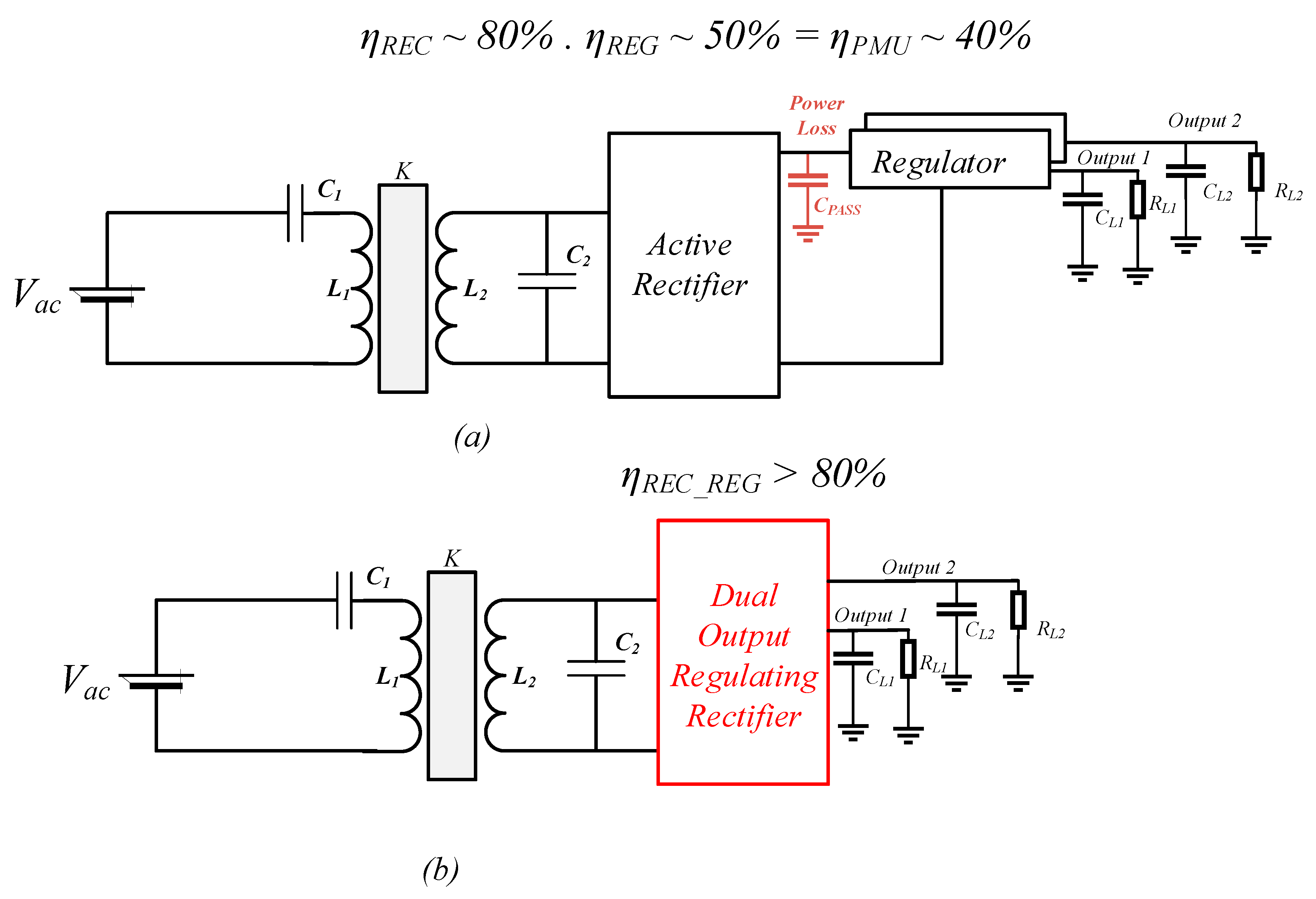
:1. Introduction
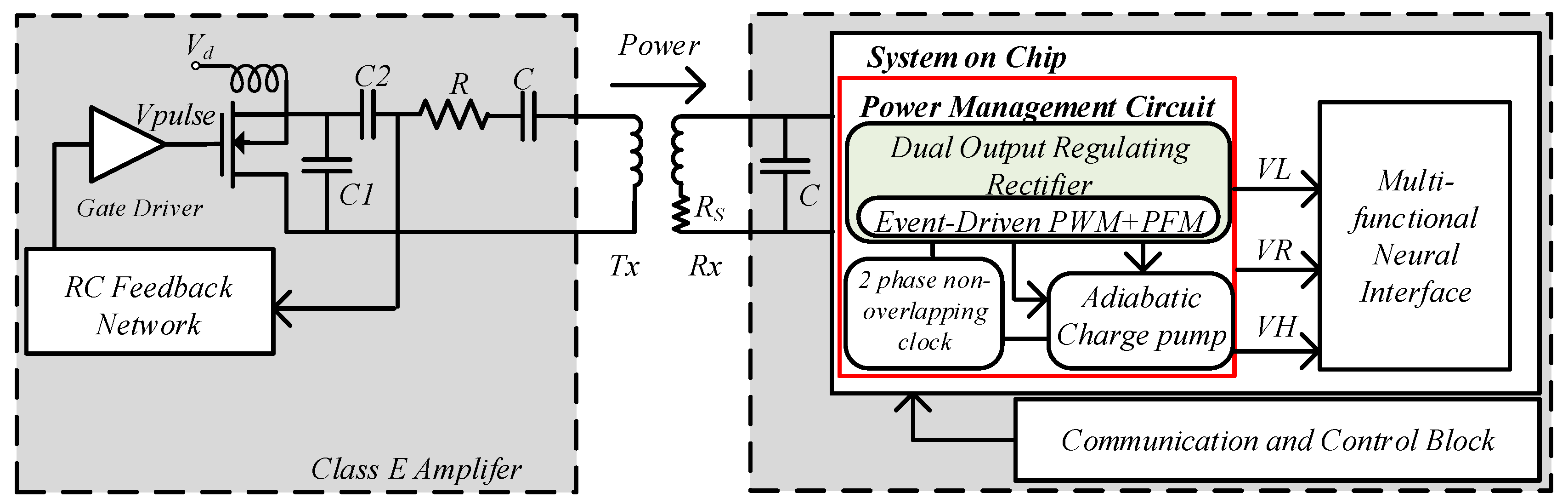
2. System Architecture and Working Principle
2.1. System Architecture
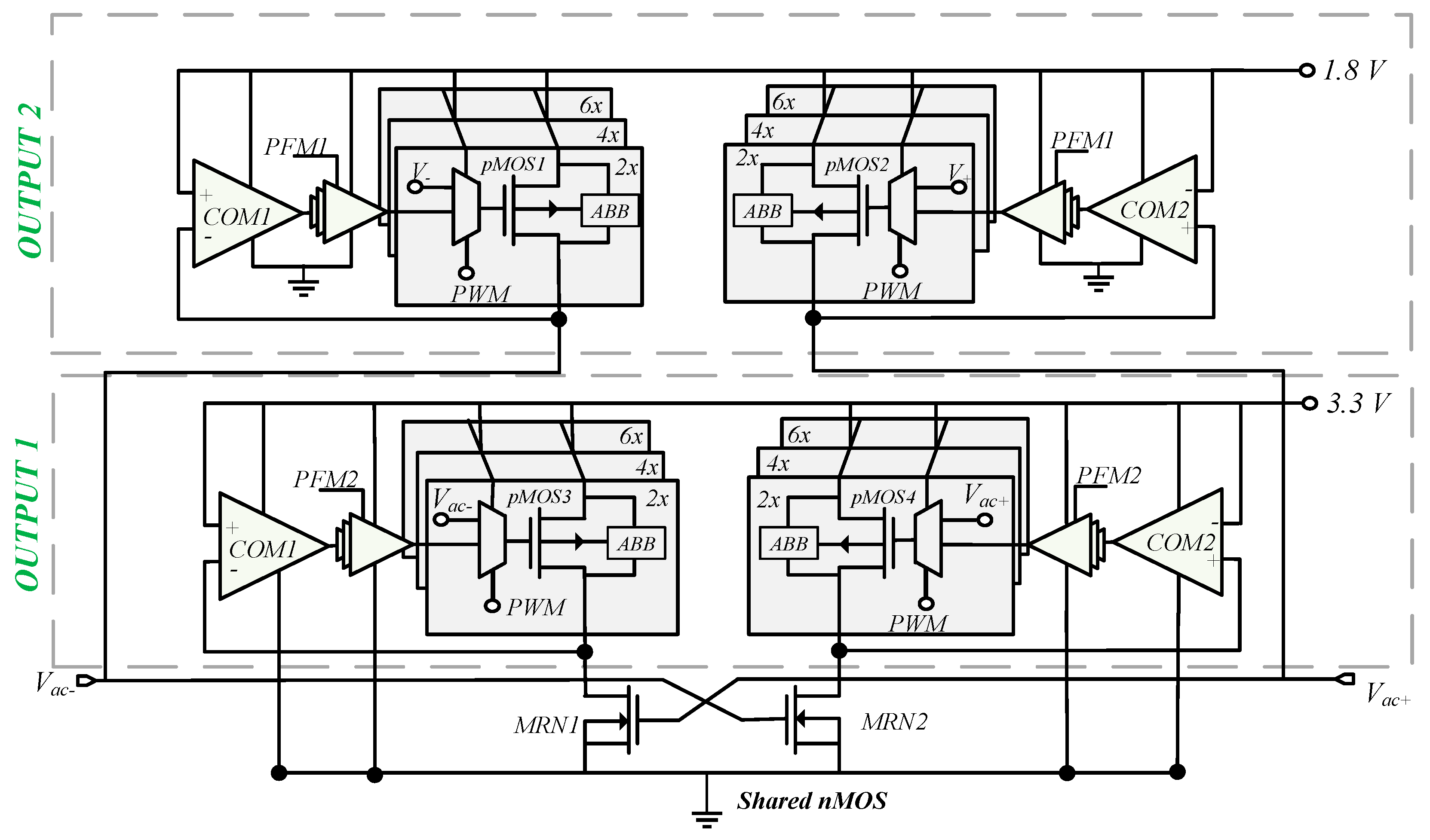
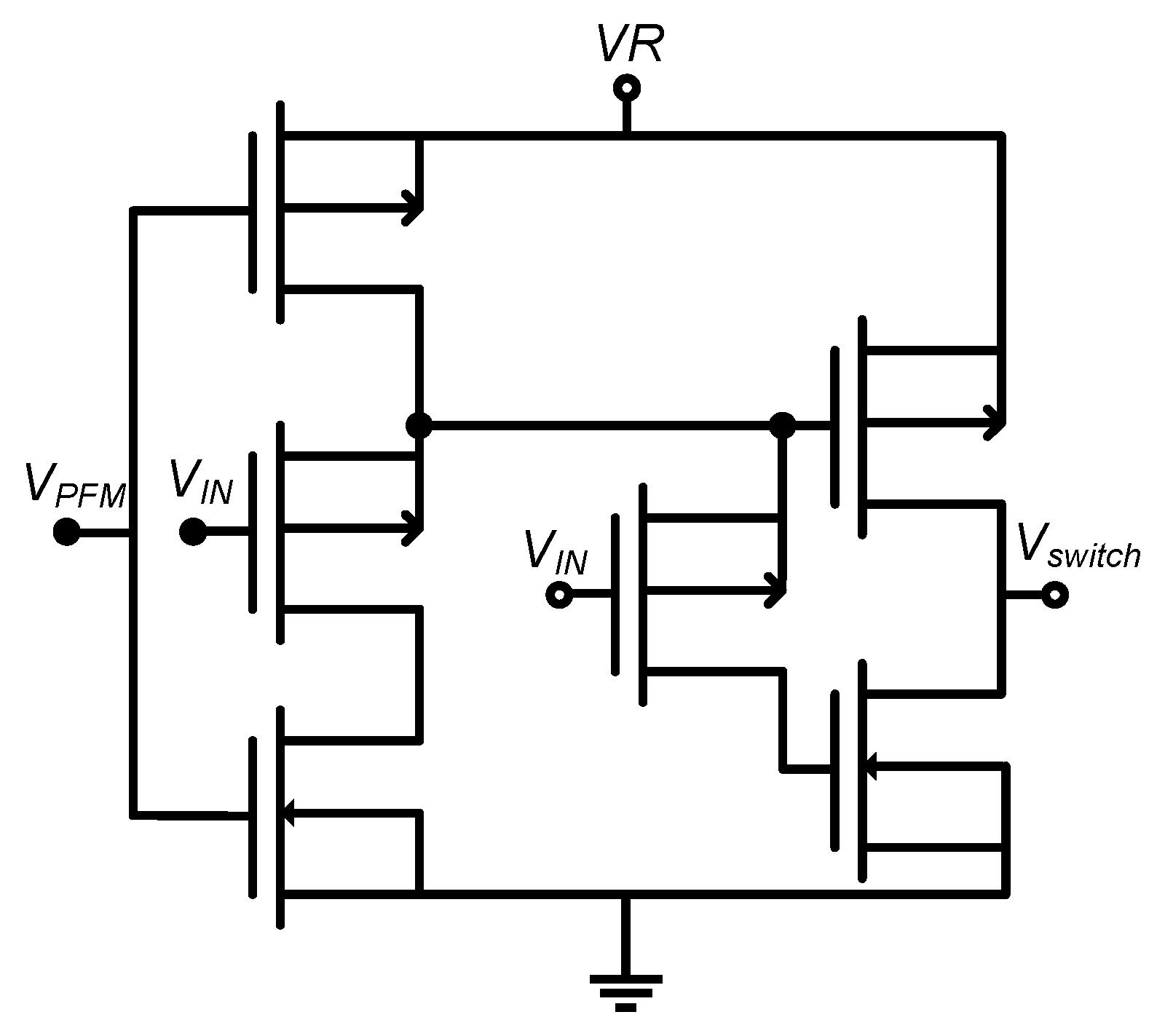
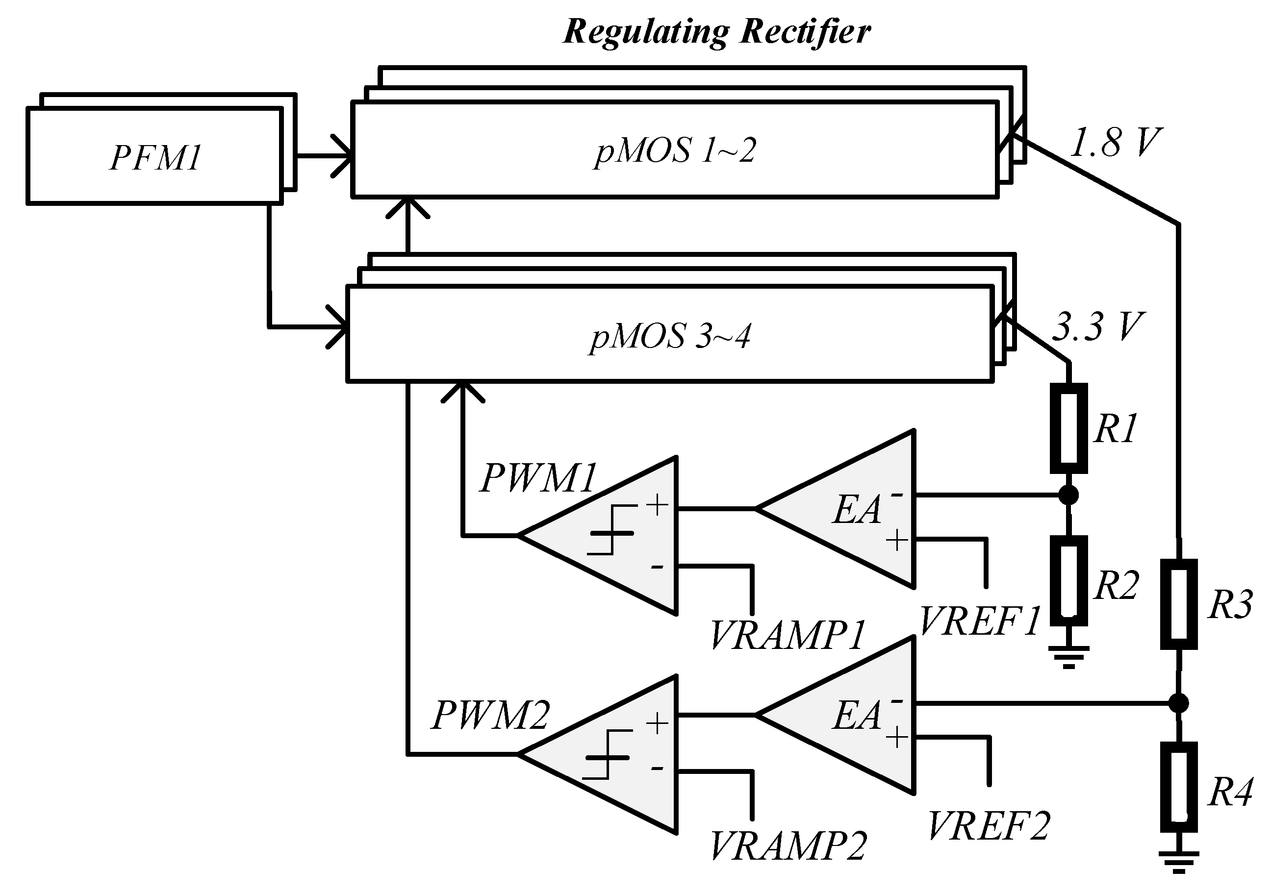
2.2. Dual Output Regulating Rectifier Architecture
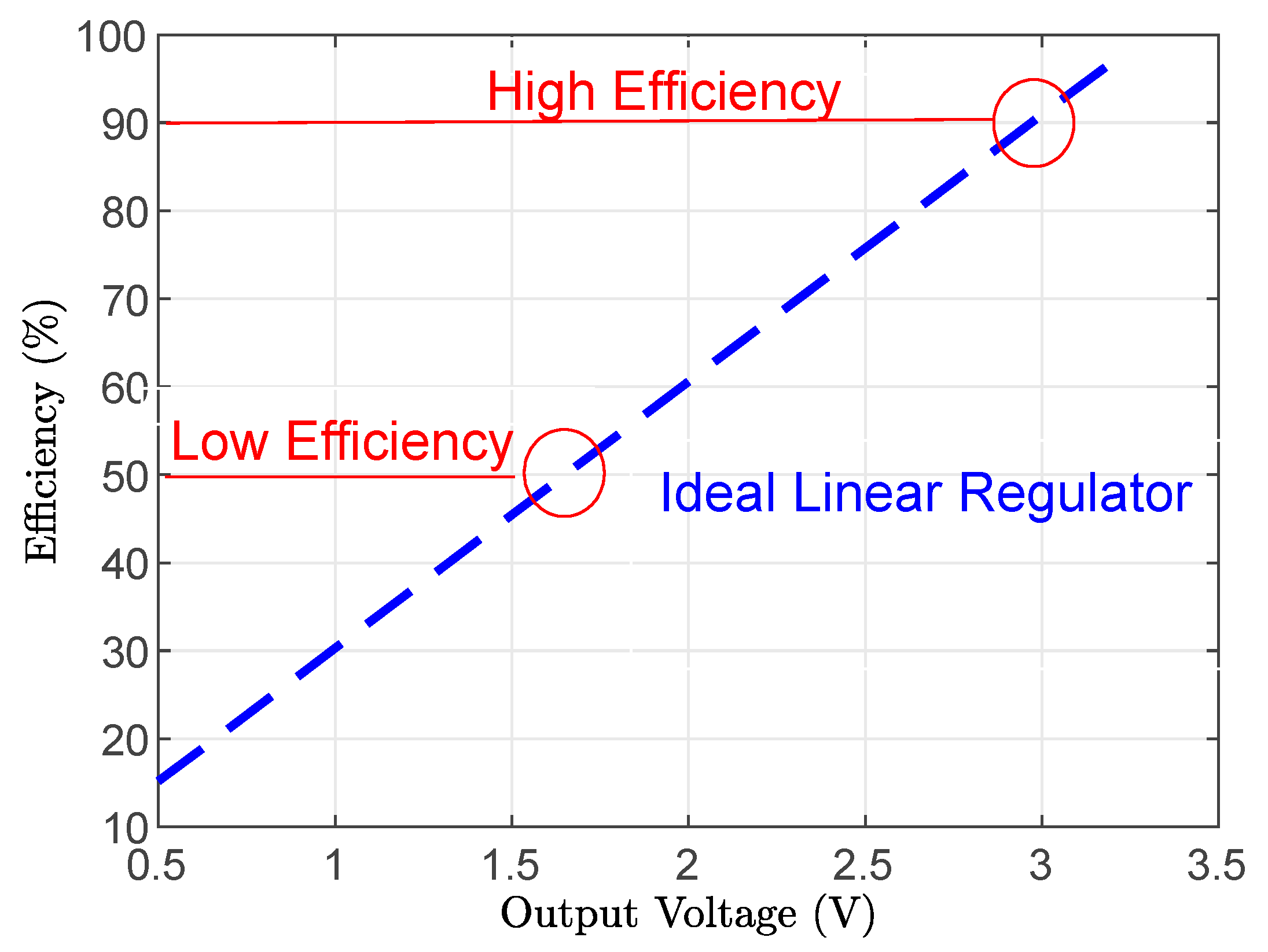
2.3. Feedback Control Analysis and Design Considerations
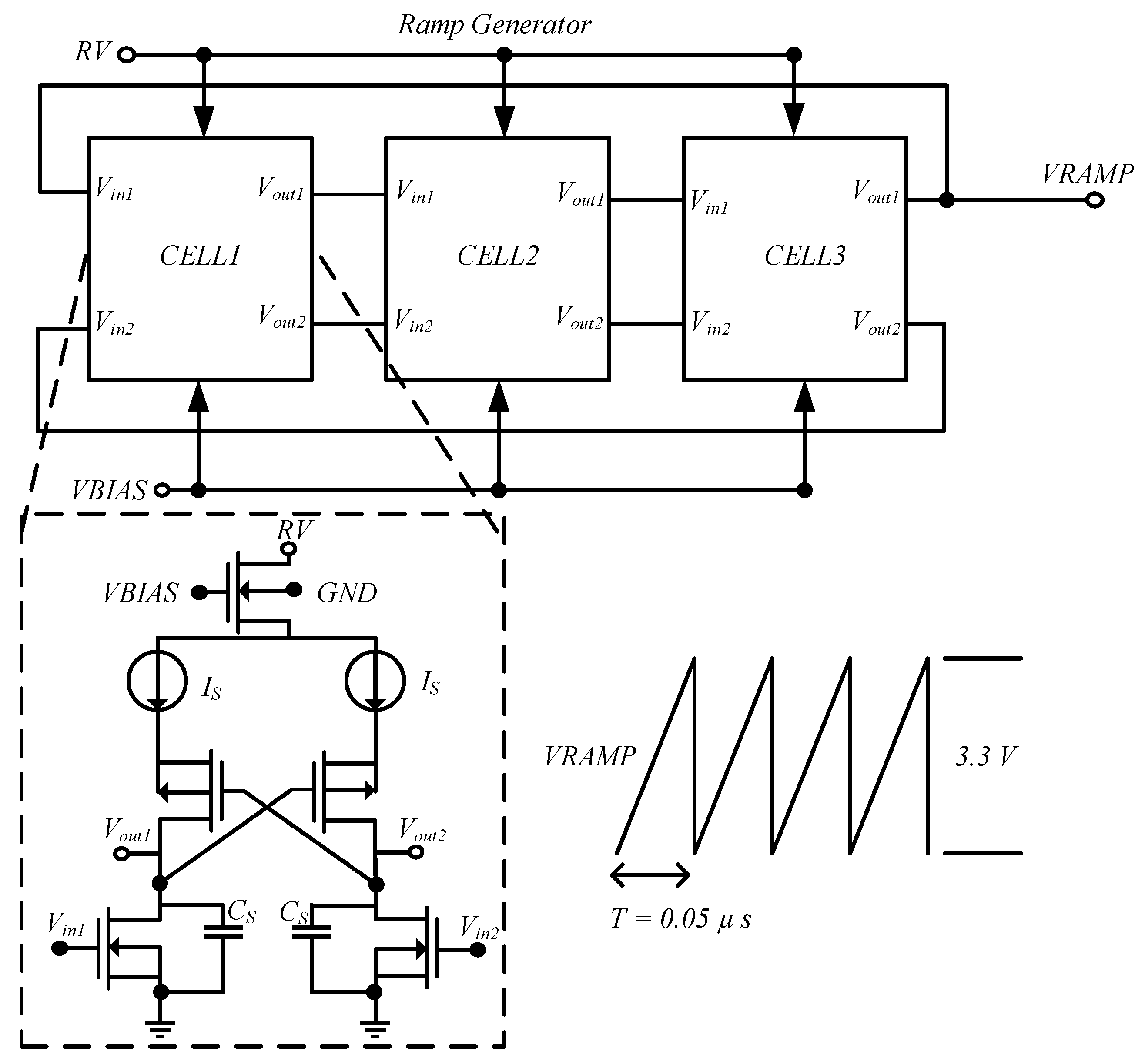
2.3.1. Pulse Width Modulation (PWM) Control
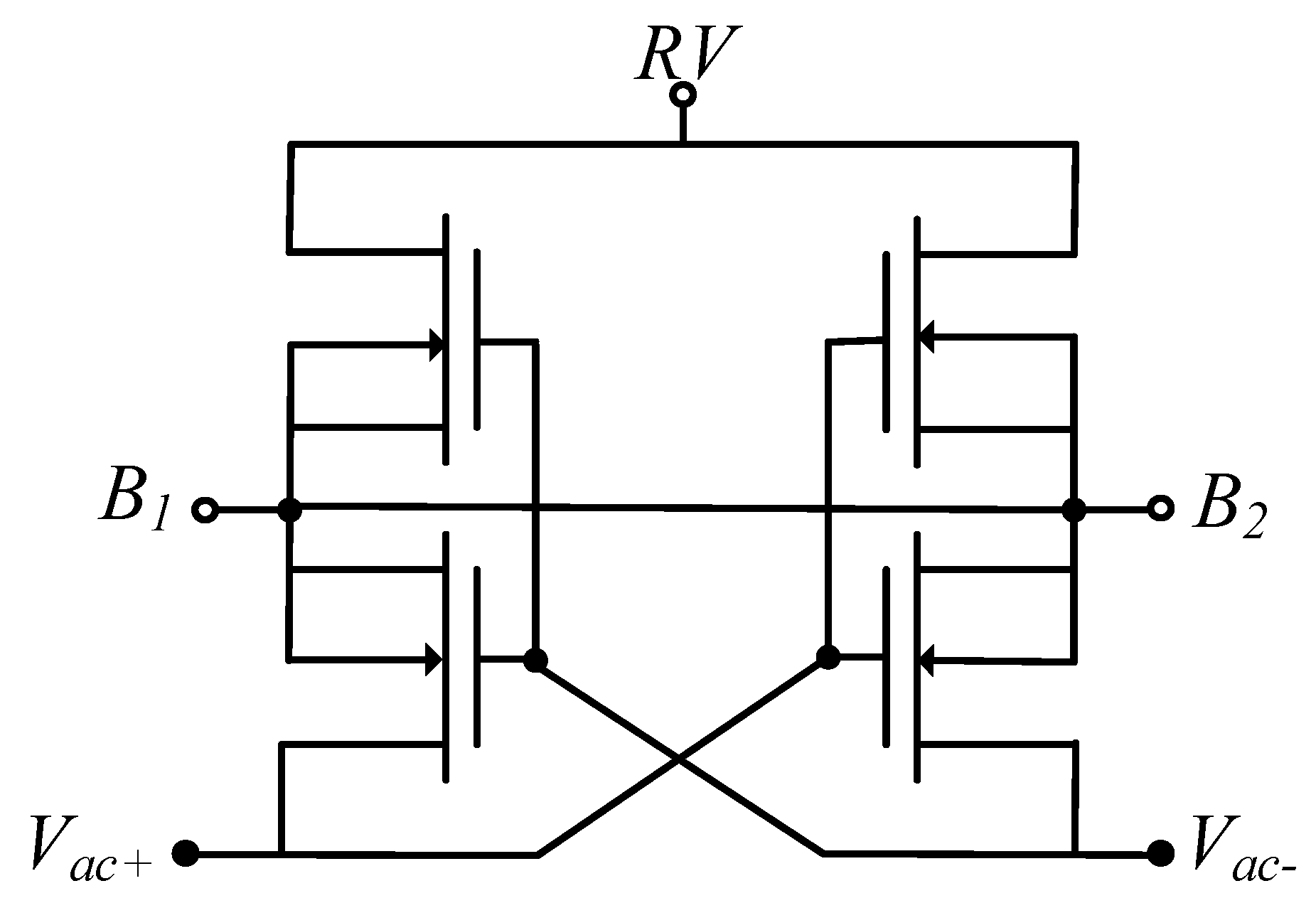
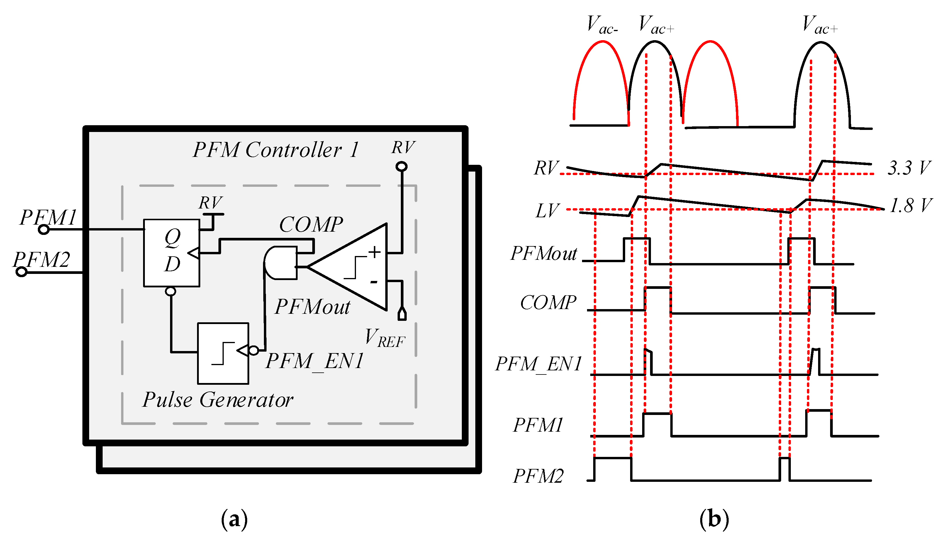
2.3.2. Pulse Frequency Modulation (PFM) Control
2.4. Charge Pump Design and Analysis
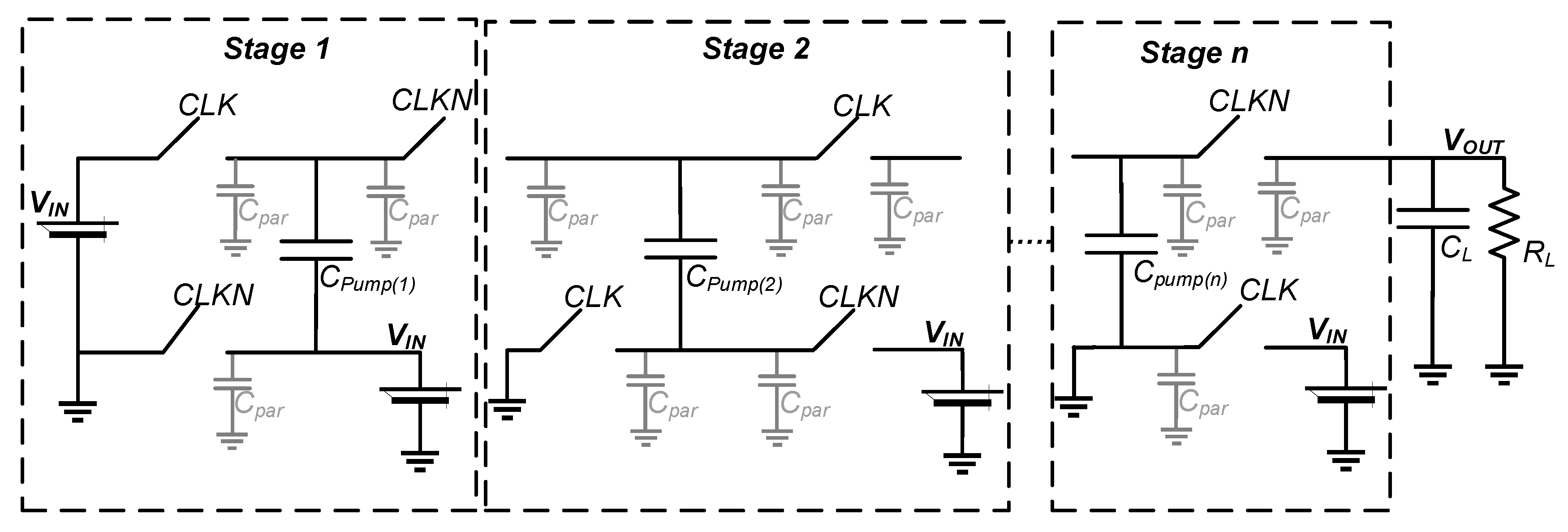
2.4.1. Charge Pump Principals
- (1)
- Slow switching limits (SSL) when all the switches and other conductive interconnects are assumed to be ideal, and the currents flowing between the input and output source and the comparators are ideal pulses, the SSL impedance is inversely proportional to the switching frequency, and the capacitors provide charge transfers without loss.
- (2)
- Fast switching limits (FSL) when the resistance of the switches, capacitors and interconnects dominate. Capacitors act as voltage sources. In such a system, the current flow occurs in a frequency-independent piecewise constant pattern.
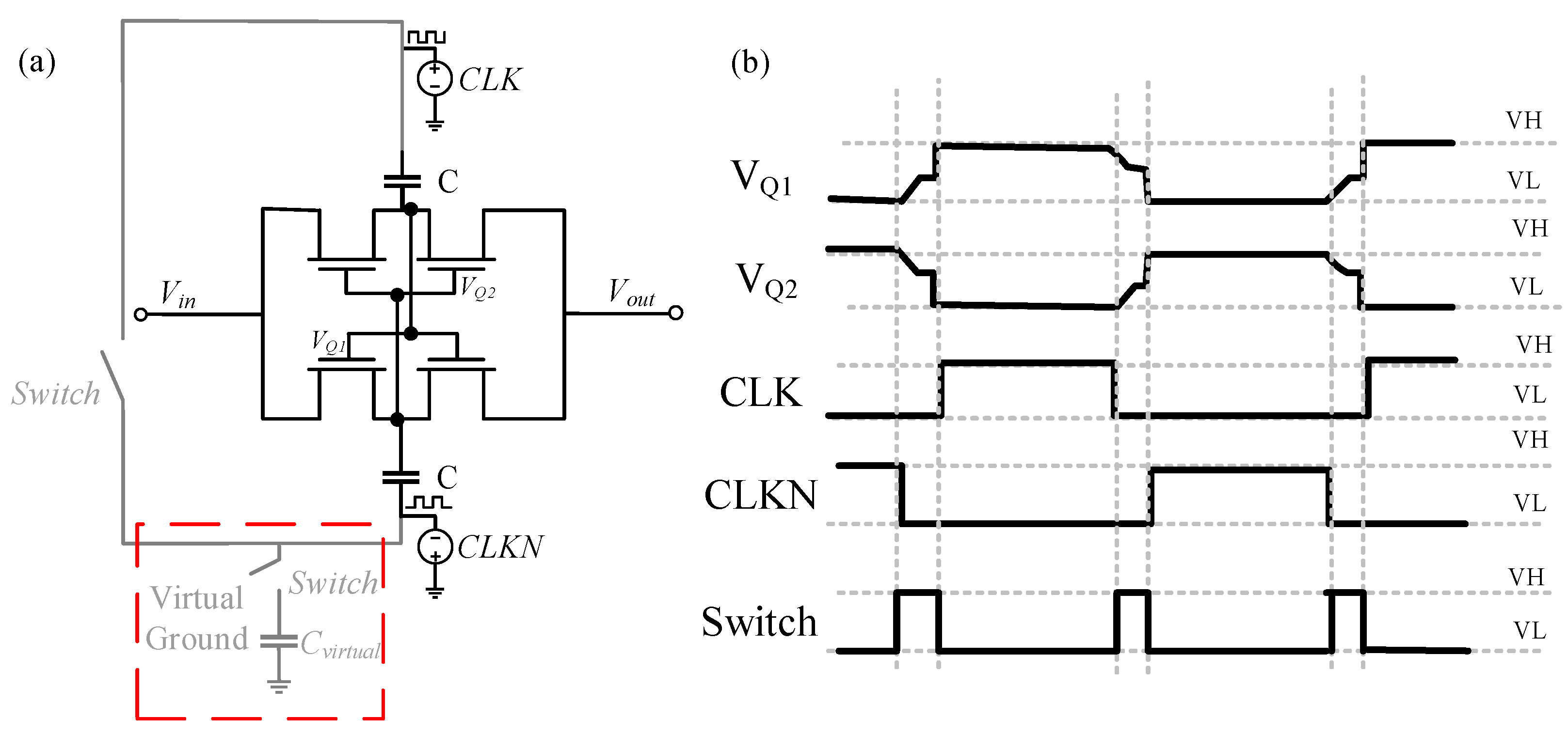
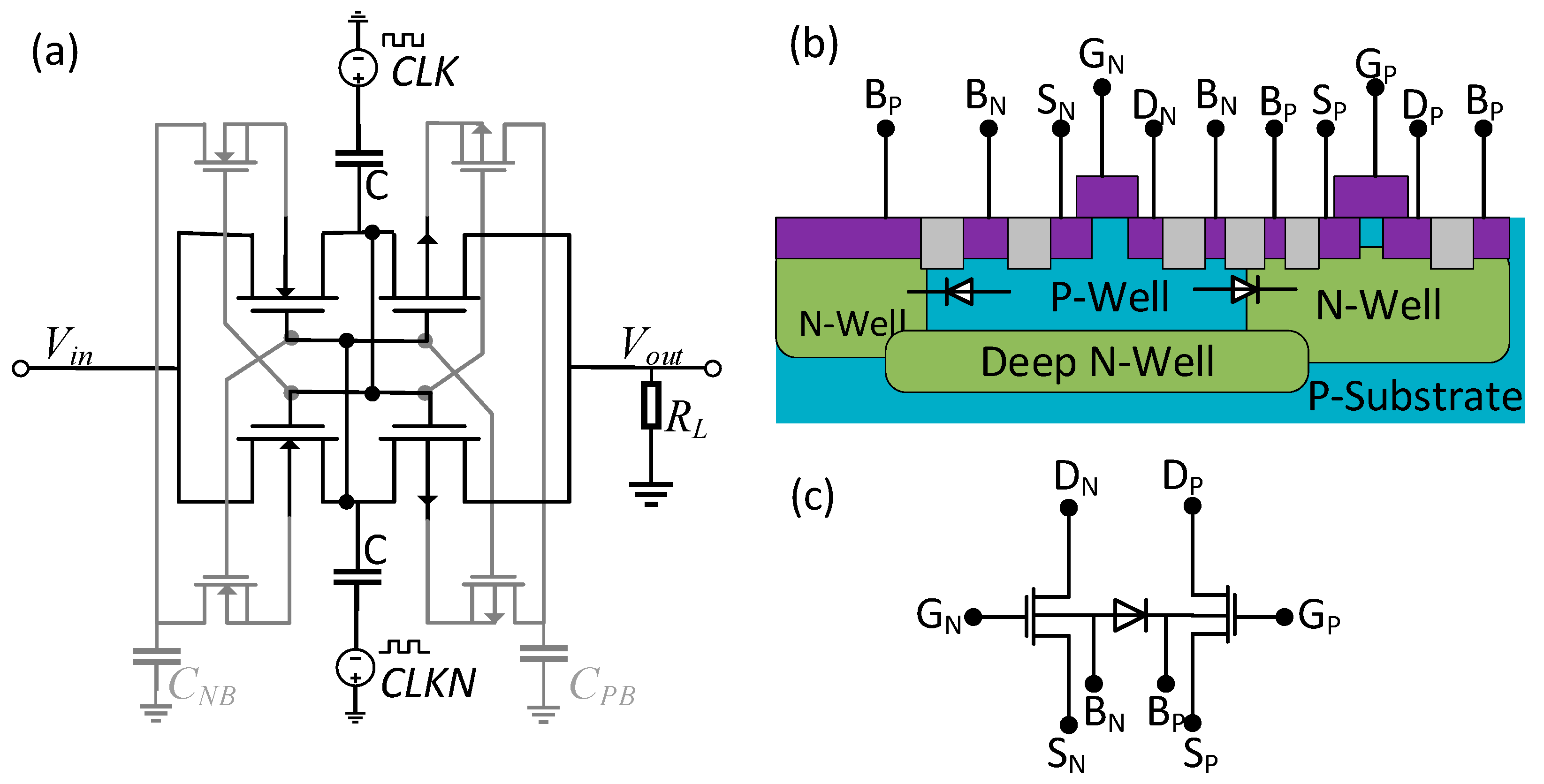
2.4.2. Adiabatic Charge Pump
3. Simulated Results
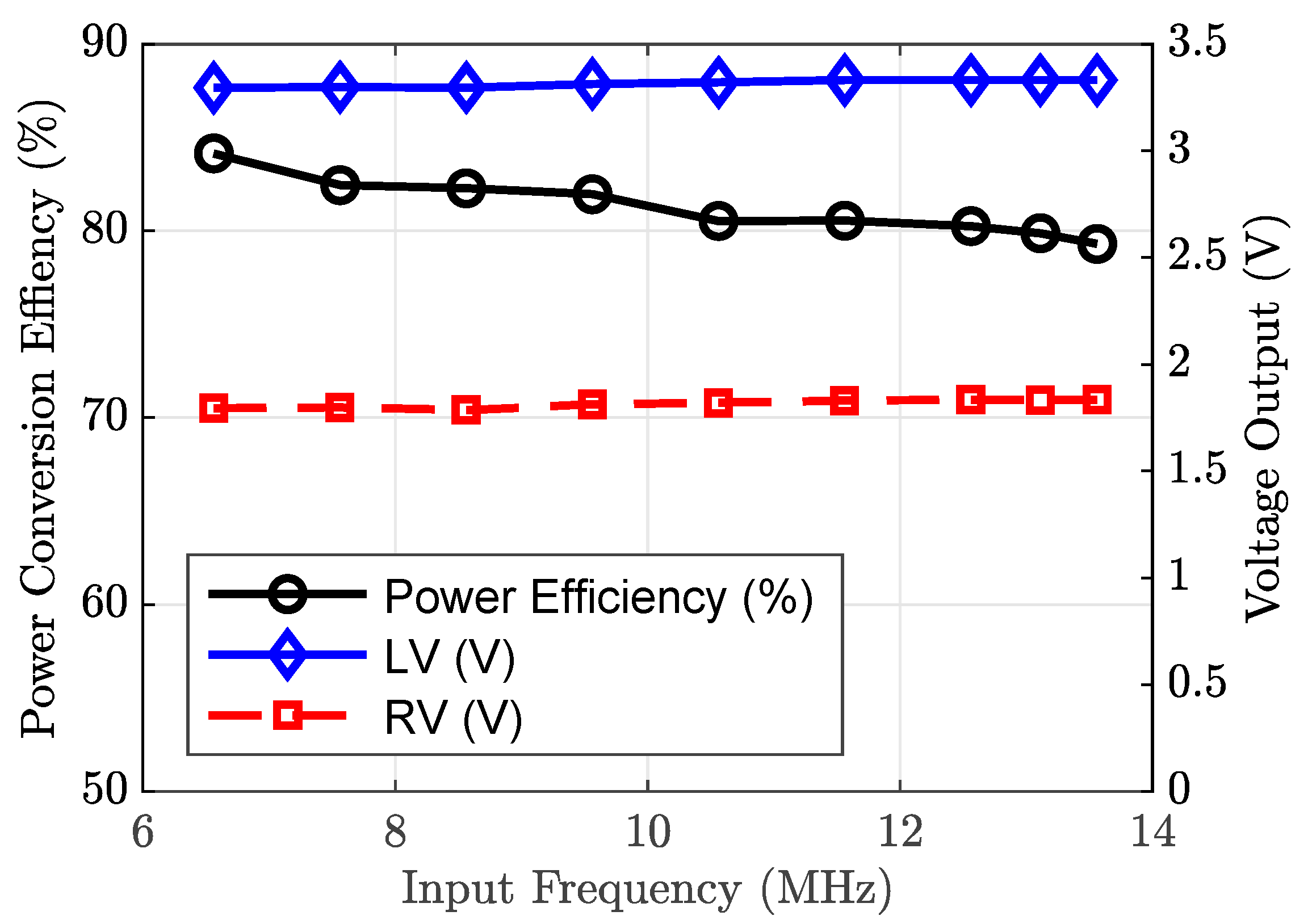
3.1. Dual Output Regulating Rectifier
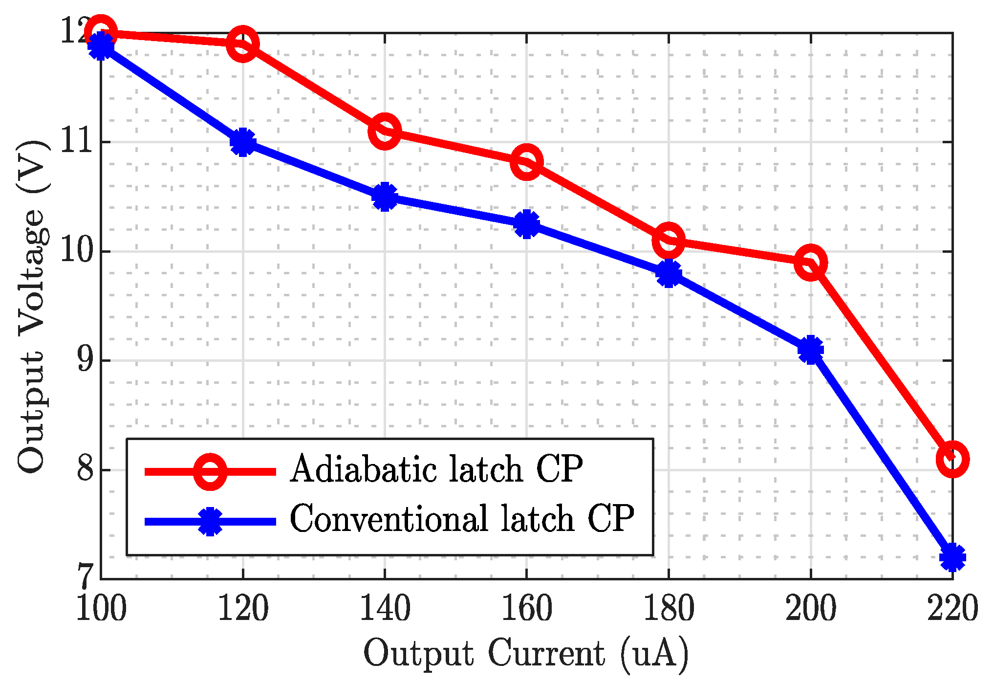
3.2. Three-Stage Adiabatic Charge Pump
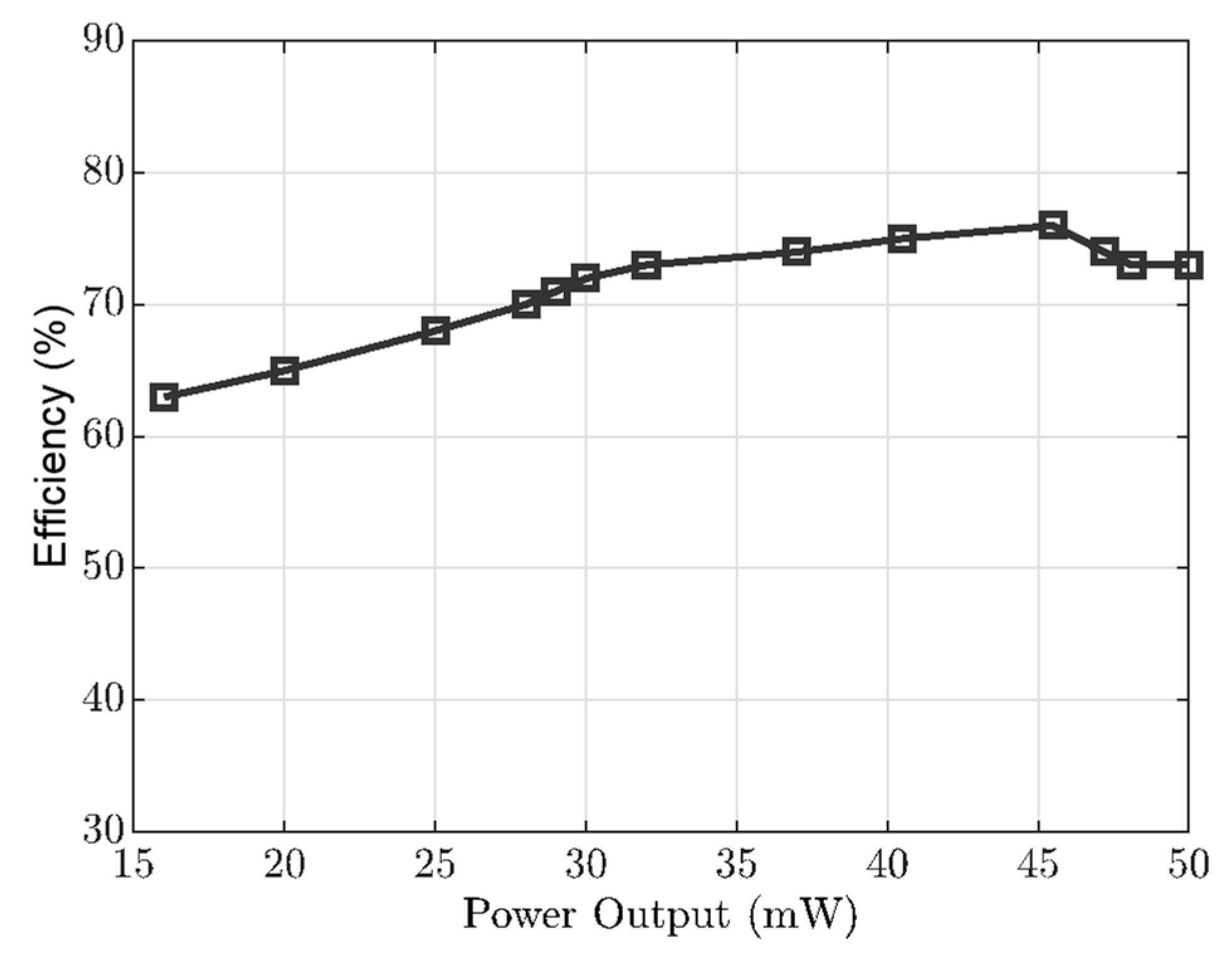
3.3. Overall System Performance and Analysis
4. Discussion
5. Conclusions
Author Contributions
Funding
Institutional Review Board Statement
Informed Consent Statement
Data Availability Statement
Conflicts of Interest
References
- Jang, J.; Habibagahi, I.; Rahmani, H.; Babakhani, A. Wirelessly powered, batteryless closed-loop biopotential recording IC for implantable leadless cardiac monitoring applications. In Proceedings of the IEEE Biomedical Circuits and Systems Conference Proceedings, Berlin, Germany, 7–9 October 2021; pp. 6–9. [Google Scholar]
- Schormans, M.; Valente, V.; Demosthenous, A. Practical inductive link design for biomedical wireless power transfer: A tutorial. IEEE Trans. Biomed. Circuits Syst. 2018, 12, 1112–1130. [Google Scholar] [CrossRef] [PubMed] [Green Version]
- Barbruni, G.L.; Motto Ros, P.; Demarchi, D.; Carrara, S.; Ghezzi, D. Miniaturised wireless power transfer systems for neurostimulation: A review. IEEE Trans. Biomed. Circuits Syst. 2020, 14, 1160–1178. [Google Scholar] [CrossRef] [PubMed]
- Pahlavan, S.; Shooshtari, M.; Jafarabadi Ashtiani, S. Star-Shaped Coils in the Transmitter Array for Receiver Rotation Tolerance in Free-Moving Wireless Power Transfer Applications. Energies 2022, 15, 8643. [Google Scholar] [CrossRef]
- Lee, B.; Jia, Y. Wirelessly-Powered Cage Designs for Supporting Long-Term Experiments on Small Freely Behaving Animals in a Large Experimental Arena. Electronics 2020, 9, 1999. [Google Scholar] [CrossRef]
- Carreon-Bautista, S.; Huang, L.; Sanchez-Sinencio, E. An autonomous energy harvesting power management unit with digital regulation for IoT applications. IEEE J. Solid-State Circuits 2016, 51, 1457–1474. [Google Scholar] [CrossRef]
- Lin, L.; Jain, S.; Alioto, M. Integrated power management for battery-indifferent systems with ultra-wide adaptation down to NW. IEEE J. Solid-State Circuits 2020, 55, 967–976. [Google Scholar] [CrossRef]
- Amin, S.S.; Mercier, P.P. MISIMO: A multi-input single-inductor multi-output energy harvester employing event-driven MPPT control to achieve 89% peak efficiency and a 60,000x dynamic range in 28 nm FDSOI. In Proceedings of the IEEE International Solid-State Circuits Conference, San Francisco, CA, USA, 11–15 February 2018; pp. 144–146. [Google Scholar]
- Lin, Y.P.; Tang, K.T. An inductive power and data telemetry subsystem with fast transient low dropout regulator for biomedical implants. IEEE Trans. Biomed. Circuits Syst. 2016, 10, 435–444. [Google Scholar] [CrossRef] [PubMed]
- Charthad, J.; Chang, T.C.; Liu, Z.; Sawaby, A.; Weber, M.J.; Baker, S.; Gore, F.; Felt, S.A.; Arbabian, A. A mm-sized wireless implantable device for electrical stimulation of peripheral nerves. IEEE Trans. Biomed. Circuits Syst. 2018, 12, 257–270. [Google Scholar] [CrossRef] [PubMed]
- Liu, F.; Wu, Y.; Almarri, N.; Habibollahi, M.; Lancashire, H.T.; Bryson, B.; Greensmith, L.; Jiang, D.; Demosthenous, A. A fully implantable opto-electro closed-loop neural interface for motor neuron disease studies. IEEE Trans. Biomed. Circuits Syst. 2022, 16, 752–765. [Google Scholar] [CrossRef]
- Jiang, D.; Wu, Y.; Almarri, N.; Habibollahi, M.; Lancashire, H.T.; Bryson, B.; Greensmith, L.; Liu, F. Demosthenous An integrated bidirectional multi-channel opto-electro arbitrary waveform stimulator for treating motor neurone disease. In Proceedings of the 2021 IEEE International Symposium on Circuits and Systems (ISCAS), Daegu, Republic of Korea, 22–28 May 2021; pp. 1–4. [Google Scholar]
- Almarri, N.; Jiang, D.; Langlois, P.; Rahal, D.M.; Demosthenous, A. High Efficiency Power Management Unit for Implantable Optical-Electrical Stimulators. In IEEE Open Journal of Circuits and Systems; IEEE: New York, NY, USA, 2023. [Google Scholar]
- Ha, S.; Gert, C.; Patrick, M.; Chul, K. High-Density Integrated Electrocortical Neural Interfaces; Academic Press: Cambridge, MA, USA, 2019. [Google Scholar]
- Almarri, N.; Jiang, D.; Demosthenous, A. Dual output regulating rectifier for an implantable neural interface. In Proceedings of the IEEE International Conference on Electronics, Circuits, and Systems (ICECS), Dubai, United Arab Emirates, 28 November–1 December 2021; pp. 7–10. [Google Scholar]
- Cheng, L.; Ki, W.H.; Lu, Y.; Yim, T.S. Adaptive on/off delay-compensated active rectifiers for wireless power transfer systems. IEEE J. Solid-State Circuits 2016, 51, 712–723. [Google Scholar]
- Talla, V.; Smith, J.R. Design and analysis of a high bandwidth rectifying regulator with PWM and PFM modes. IEEE Trans. Circuits Syst. II Express Briefs 2016, 63, 1121–1125. [Google Scholar] [CrossRef]
- Sun, Z.; Siek, L. A novel ripple controlled modulation for high efficiency dc-dc converters. In Proceedings of the International Symposum of Integrated Circuits, (ISIC), Singapore, 12–14 December 2011; pp. 238–241. [Google Scholar]
- Tanzawa, T.; Tanaka, T. A dynamic analysis of the dickson charge pump circuit. IEEE J. Solid-State Circuits 1997, 32, 1231–1240. [Google Scholar] [CrossRef]
- Cabrini, A.; Gobbi, L.; Torelli, G. Voltage gain analysis of integrated fibonacci-like charge pumps for low power applications. IEEE Trans. Circuits Syst. II Express Briefs 2007, 54, 929–933. [Google Scholar] [CrossRef]
- Chang, L.K.; Hu, C.H. High efficiency MOS charge pumps based on exponential-gain structure with pumping gain increase circuits. IEEE Trans. Power Electron 2006, 21, 826–831. [Google Scholar] [CrossRef]
- Lauterbach, C.; Weber, W.; Römer, D. Charge sharing concept and new clocking scheme for power efficiency and electromagnetic emission improvement of boosted charge pumps. IEEE J. Solid-State Circuits 2000, 35, 719–723. [Google Scholar] [CrossRef]
- Ker, M.D.; Chen, S.L.; Tsai, C.S. Design of charge pump circuit with consideration of gate-oxide reliability in low-voltage CMOS processes. IEEE J. Solid-State Circuits 2006, 41, 1100–1107. [Google Scholar] [CrossRef] [Green Version]
- Ballo, A.; Grasso, A.D.; Palumbo, G. A high-performance charge pump topology for very-low-voltage applications. IEEE Trans. Circuits Syst. II Express Briefs 2020, 67, 1304–1308. [Google Scholar] [CrossRef]
- Palumbo, G.; Pappalardo, D. Charge Pump Circuits: An overview on design strategies and topologies. IEEE Circuits Syst. Mag. 2010, 10, 31–45. [Google Scholar] [CrossRef]
- Abdi, A.; Kim, H.S.; Cha, H.K. A high-voltage generation charge-pump IC using input voltage modulated regulation for neural implant devices. IEEE Trans. Circuits Syst. II Express Briefs 2018, 66, 342–346. [Google Scholar] [CrossRef]
- Lenstra, A.K.; Shamir, A. Analysis and optimization of switched-capacitor dc-dc converters. IEEE Trans. Power Electron. 2008, 23, 841–851. [Google Scholar]
- Ulaganathan, C.; Blalock, B.J.; Holleman, J.; Britton, C.L. An ultra-low voltage self-startup charge pump for energy harvesting applications. In Proceedings of the International Midwest Symposium on Circuits and Systems (MWSCAS), Boise, ID, USA, 5–8 August 2012; pp. 206–209. [Google Scholar]
- Xue, Z.; Fan, S.; Zhang, L.; Guo, Z.; Dong, L.; Li, D.; Geng, L. Single-stage dual-output ac-dc converter for wireless power transmission. In Proceedings of the IEEE Custom Integrated Circuits Conference (CICC), San Diego, CA, USA, 8–11 April 2018; pp. 1–4. [Google Scholar]
- Low, Q.W.; Siek, L. A single-stage dual-output tri-mode ac-dc regulator for inductively powered application. IEEE Trans. Circuits Syst. I Regul. Pap. 2019, 66, 3620–3630. [Google Scholar] [CrossRef]
- Gougheri, H.S.; Graybill, P.; Kiani, M. A dual-output reconfigurable shared-inductor boost-converter/current-mode inductive power management ASIC with 750% extended output-power range, adaptive switching control, and voltage-power regulation. IEEE Trans. Biomed. Circuits Syst. 2019, 13, 1075–1086. [Google Scholar] [CrossRef]
- Erfani, R.; Marefat, F.; Mohseni, P. A dual-output single-stage regulating rectifier with PWM and dual-mode PFM control for wireless powering of biomedical implants. IEEE Trans. Biomed. Circuits Syst. 2020, 14, 1195–1206. [Google Scholar] [CrossRef] [PubMed]
- Goeppert, J.; Manoli, Y. Fully integrated startup at 70 MV of boost converters for thermoelectric energy harvesting. IEEE J. Solid-State Circuits 2016, 51, 1716–1726. [Google Scholar] [CrossRef]
- Yi, H.; Yin, J.; Mak, P.I.; Martins, R.P. A 0.032-Mm2 0.15-V Three-stage charge-pump scheme using a differential bootstrapped ring-VCO for energy-harvesting applications. IEEE Trans. Circuits Syst. II Express Brief 2018, 65, 146–150. [Google Scholar] [CrossRef]
- Fuketa, H.; O’Uchi, S.I.; Matsukawa, T. Fully integrated, 100-Mv minimum input voltage converter with gate-boosted charge pump kick-started by LC oscillator for energy harvesting. IEEE Trans. Circuits Syst. II Express Briefs 2017, 64, 392–396. [Google Scholar] [CrossRef]
- Mahmoud, A.; Alhawari, M.; Mohammad, B.; Saleh, H.; Ismail, M. A charge pump based power management unit with 66%-efficiency in 65 Nm CMOS. In Proceedings of the IEEE International Symposium of Circuits Systems (ISCAS), Florence, Italy, 27–30 May 2018; pp. 1–4. [Google Scholar]
- With, H.; Shih, Y.; Member, S.; Otis, B.P.; Member, S. An inductorless dc–dc converter for energy output controller. In IEEE Transactions on Circuits and Systems II: Express Briefs; IEEE: New York, NY, USA, 2011; pp. 832–836. [Google Scholar]
- Luo, Z.; Ker, M.; Cheng, W.; Yen, T. Regulated Charge Pump With New Clocking Scheme for Smoothing the Charging Current in Low Voltage CMOS Process. IEEE Trans. Circuits Syst. I Regul. Pap. 2017, 64, 528–536. [Google Scholar] [CrossRef]


| PWM | PFM | Operation Mode |
|---|---|---|
| OFF | OFF | Diode connected |
| ON | OFF | Comparators connected |
| OFF | ON | Frequency decreased. Power saving mode |
| ON | ON | Frequency decreased |
| [29] | [30] | [31] | [32] | This Work | |
|---|---|---|---|---|---|
| Process (nm) | 180 | 180 | 180 | 180 | 180 |
| Freq. (MHz) | 13.56 | 0.0125 | 1 | 1–10 | 13.56 |
| Vin_ac (V) | 1.35~1.8, 2.15~2.8 | 1.6~2 | NA | 1.5~2.5 | 1.5–3.5 |
| Regulation Topology | Delay-based Rectifier | SSDO Tri-mode | Voltage power Reg. | Regulating Rectifier | Regulating Rectifier |
| Vdc (V) | 3.12 | 3.6 | 1 | 1.5–2.5 | 1.8–3.3 |
| RL1,2 (kΩ) | 0.5 | 0.2,1 | 8 | 0.1 | 0.33–1 |
| Pout, Max (mW) | 10 | 114 | 4.7 | 65 | 40.5 |
| VCE (%) | 82.2 | NA | 92 | 75.8 | 94.3 |
| PCE Peak (%) | 79 | 91.7 | 75.3 | 90.75 | 82.3 |
| [33] | [34] | [35] | [36] | [37] | [38] | [22] | This Work | |
|---|---|---|---|---|---|---|---|---|
| Process (nm) | 130 | 65 | 65 | 65 | 130 | 180 | 130 | 180 |
| Topology | Linear | Linear | Boot- Strap | Dickson | Bootstrap | Bootstrap | Adiabatic | Adiabatic |
| No. of Stages | 6 | 3 | 10 | 4 | 3 | 3 | 7 | 3 |
| Clock Freq (MHz) | 0.040 | 15.2 | 10 | 1.8 | 0.8 | 86.1 | 0.36 | 10 |
| Total Cap. (pF) | 46.08 | 22.5 | 1001 | 160 | 150 | 400 | 100 | 60 |
| Load current (μA) | 12 | 1.74 | 0.76 | 10 | 5 | 500 | 0.1 | 100 |
| Max power (μW) | 15 | 1.5 | 6.6 | 4.7 | 7 | 3675 | 0.035 | 1200 |
| PCE (%) | 58 | 38.8 | 33 | 66 | 58 | 69 | 59–62 | 82.9 |
Disclaimer/Publisher’s Note: The statements, opinions and data contained in all publications are solely those of the individual author(s) and contributor(s) and not of MDPI and/or the editor(s). MDPI and/or the editor(s) disclaim responsibility for any injury to people or property resulting from any ideas, methods, instructions or products referred to in the content. |
© 2023 by the authors. Licensee MDPI, Basel, Switzerland. This article is an open access article distributed under the terms and conditions of the Creative Commons Attribution (CC BY) license (https://creativecommons.org/licenses/by/4.0/).
Share and Cite
Almarri, N.; Langlois, P.; Jiang, D.; Demosthenous, A. Efficient Dual Output Regulating Rectifier and Adiabatic Charge Pump for Biomedical Applications Employing Wireless Power Transfer. J. Low Power Electron. Appl. 2023, 13, 20. https://doi.org/10.3390/jlpea13010020
Almarri N, Langlois P, Jiang D, Demosthenous A. Efficient Dual Output Regulating Rectifier and Adiabatic Charge Pump for Biomedical Applications Employing Wireless Power Transfer. Journal of Low Power Electronics and Applications. 2023; 13(1):20. https://doi.org/10.3390/jlpea13010020
Chicago/Turabian StyleAlmarri, Noora, Peter Langlois, Dai Jiang, and Andreas Demosthenous. 2023. "Efficient Dual Output Regulating Rectifier and Adiabatic Charge Pump for Biomedical Applications Employing Wireless Power Transfer" Journal of Low Power Electronics and Applications 13, no. 1: 20. https://doi.org/10.3390/jlpea13010020