1. Introduction
The dissemination of Internet-of-Things (IoTs)-like wireless sensors or other tiny computing machines is facing a serious issue regarding the power supply. Batteries are no longer a suitable choice, or at least the effective lifespan must be enlarged as much as possible. Harvesting energy in the IoT environment is investigated. Among the possible sources of ambient energy, the electromagnetic field yields a weaker potential but is still significant. An electromagnetic field harvester comprises four blocks to convert radio-frequency (RF) energy to direct-current (DC) energy, namely an antenna, a matching network, a rectifier and a voltage converter. Shape of antenna, topology of matching network, rectifier or voltage converter, or combination of functions have been studied to create simple to complex systems.
A review of radio-frequency energy harvester (RFEH) design is given in [
1]. Most RFEHs have been considered for a frequency range below 5 GHz, though microwave applications have been reported recently [
2]. The major metrics of performances are the minimum input RF power that can start-up the EH system, the open-voltage at the targeted input RF power level and the effective efficiency when the rectenna is loaded with an impedance equal to its internal impedance (optimal load condition) [
3].
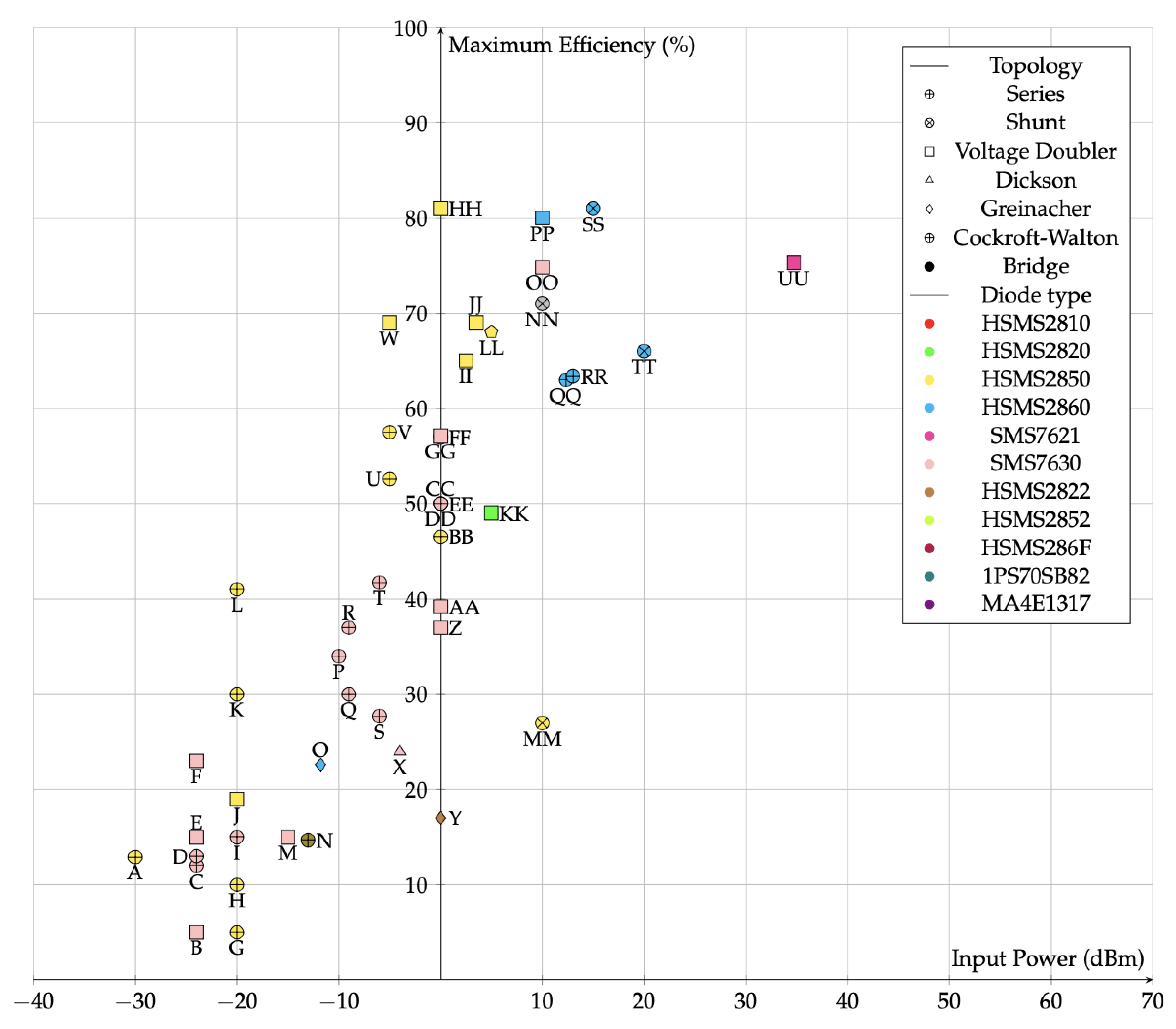
Figure 1 pictures a landscape of representative results of the rectenna from the literature, where the maximum efficiency is mentioned along with the related input RF power level [
4,
5]. The results are related to demonstrators obtained through a traditional 2D process. The results are discriminated depending on the rectifier topology and the selected diode. Colors and symbols identify the various results in
Figure 1. At low input RF power (<−20 dBm), one-diode topology (symbols ⊕ and ⊗ in
Figure 1) is mostly preferred among the well-known topologies (single series, single shunt, voltage doubler, Dickson topology, Cockcroft-Walton topology, Diode bridge topology, Villard charge pump topology, etc). The two-diode topology is proposed at medium input RF power (0 dBm) for implementing voltage doubling effect. The maximum efficiency is in direct relation with the input RF power: more input voltage enables to better bias the diodes (or even MOSFET transistors in the case of integrated circuit implementations). Complex rectifier topologies are considered for input RF power levels well above 0 dBm. The selection of diode is spread among the different results. However, the references HSMS2850 and SMS7621 dominate at low input RF power.
Ambient RF energy harvesting is related to a case of low RF power. In this condition, the expected DC voltage at the rectenna output is quite low and supplying a (low-power) circuit requires at least 1 V as an order of magnitude with respect to CMOS electronics. Multi-level topologies have been experimented, but due to diode forward voltage drop, a quite high level of input RF power is necessary [
6].
Most papers consider 50
rectenna for ease of design and characterization. It was already demonstrated that a different value of characteristic impedance would be beneficial in the case of very low ambient RF energy [
7]. The situation is more complex with respect to design and test and it is not considered here.
The matching network between the antenna and the rectifier relies on micro-strip implementation as it reduces the bill-of-material. Demonstrators in the literature are fabricated on substrates for which dielectric performances (losses) are quite optimal, i.e., close to Rogers’ substrates ones. Some exploratory studies are carried out on FR4 for the sake of cost, but it is not a game-changer yet. Other substrates such as paper [
8] have also been experimented and the losses of the dielectric impact the rectenna performances in quite the same way as the one reported in this paper.
Antenna geometries benefit from constant improvement with original shapes in 2D or 3D. The literature covers few proposals of antenna or rectennas [
5,
9] obtained from a combination of additive manufacturing to create the device substrate and through metallization to obtain the conductive traces. Otherwise, adding an RFEH capability to an existing IoT object is not simple if it should be obtained seamlessly [
1]. Besides, IoT objects may offer a package with a sufficient external surface for implementing an antenna and receiving additional devices related to the RFEH. It is an issue of selective metallization. This idea is already investigated with wearable IoTs [
10]. In this context, the prototypes are fabricated using additive manufacturing, namely 3D printing and deposition of conductive inks. The conductivity of ink is pointed to as a limitation.
The literature covers few proposals of antennas obtained from additive manufacturing. Moreover, additive manufacturing [
11] is preferred for the manufacturing of low-count series of IoTs or when prototyping an IoT object. Additive manufacturing is in use regarding cellphone antennas or 5G-related antennas [
12,
13]. In the same perspective, the paper focuses on the capability of adding an RFEH capability to an existing object package or housing using 3D plastronic prototyping of the objects. Indeed, the polymer material involved in the additive manufacturing as well as the added conductor have a major impact on the RFEH performances and it is one of the main issues of the paper to quantify the impact and discuss the pertinence of the manufacturing process proposal in this context.
Figure 1.
Recent State of the art on rectifier: Maximum Efficiency vs Input Power depending on topology and diode reference. A-[
14], B-[
15], C-[
16], D-[
17], E-[
15], F-[
15], G-[
8], H-[
8], I-[
18], J-[
19], K-[
20], L-[
21], M-[
22], N-[
4], O-[
23], P-[
24], Q-[
25], R-[
25], S-[
26], T-[
26], U-[
27], V-[
27], W-[
28], X-[
29], Y-[
30], Z-[
31], AA-[
32], BB-[
33], CC-[
33], DD-[
34], EE-[
9], FF-[
35], GG-[
32], HH-[
36], II-[
28], JJ-[
37], KK-[
5], LL-[
19], MM-[
38], NN-[
39], OO-[
31], PP-[
40], QQ-[
41], RR-[
42], SS-[
43], TT-[
44], UU-[
45].
3D Plastronics allows integrating electronic functions at the surface of the polymer housing of an object by selective metallization of conductive traces and placement of Surface Mount Devices (SMD) [
46,
47]. 3D Plastronics is the terminology now accepted by the IPC organization [
48], but it is also known as Molded Interconnect Devices or Mechatronic Integrated Devices (MID) [
47]. It plays an important role in different application domains, such as miniaturization of electronic devices [
49], thermal management [
50], medical equipment’s [
46], automotive [
51] or telecommunications [
52]. Rapid 3D Plastronics is a new method in the field of additive manufacturing. The strategy is based on the manufacturing of the polymer support by 3D printing (often Stereolithography) and selective metallization by electroless copper (Cu).
This paper details the design and measurement of an RFEH vehicle fabricated on a substrate using a 3D stereolithography printing method (SLA) associated to electroless copper deposition (EDL) as a rapid prototyping process. SLA resin is not recyclable yet, including the one considered in the case study but on the one hand printing is inexpensive and straightforward, and on the other hand treatment toward recyclability is progressing.
This paper discusses gradually the main aspects of a rectenna (antenna, rectifier, voltage conversion), given a material and a manufacturing process that are not supposed to be suitable for RF applications. The sections cover the aspects sequentially with results for a partial conclusion. The paper content is organized as follows.
Section 2 details the two-transmission-line method introduced to evaluate the electromagnetic properties of the printed substrate. A simple patch antenna supports a comparison between Rogers substrate and the printed one to confirm the applicability to RF applications.
Section 3 details a modified patch antenna and the array of four-antenna.
Section 4 covers the series, one diode rectifier with a particular focus on the internal impedance of the rectifier as it is a major parameter for the power management unit.
Section 5 summarizes the design of the power management circuit deduced from the literature.
Section 6 details important system-level measurements and comparison to the state of the art. The principal knowledge deduced from the case study is discussed prior to the conclusion.
3. Modified Patch Antenna and Array of Four Antennas
A circularly polarized antenna is considered to capture the electromagnetic field around the IoT object. The package of the IoT object at hand will define the available surface. In the ideal case of a regular 3D package outside surface, such an antenna may be synthesized as an array of four antennas, regularly disposed around the object package. Arrays of multiple but small antennas have been covered but the limit in manufacturing accuracy should be considered first. This issue is clearly discussed in [
58]. The design methodology takes care of the antenna design, the isolation factor between antennas but does not consider the complexity of manufacturing. Moreover, Table IV in [
58] indicates that the combined DC power from the antennas in the array tends to decrease when the number of antennas is larger than 4.
The square patch is selected for ease of design. However, the complexity of the antenna design is not a limitation in terms of manufacturing here. Thus, all the geometries considered in [
58] could be fabricated without specific issues. A similar cylindrical arrangement of square patches is fabricated on a flexible RO5880 substrate with thickness of 0.72 mm and relative permittivity of 2.2 in [
59].
The same Schottky diode (SMS7630) will be selected later on in
Section 4, and the rectenna load is chosen to be 5.1 k
, close to the junction resistance of the diode [
60]. A measurement detailed in
Section 4 shows that a different choice of resistor value should be considered.
3.1. Modified Patch Antenna for Circular Polarization
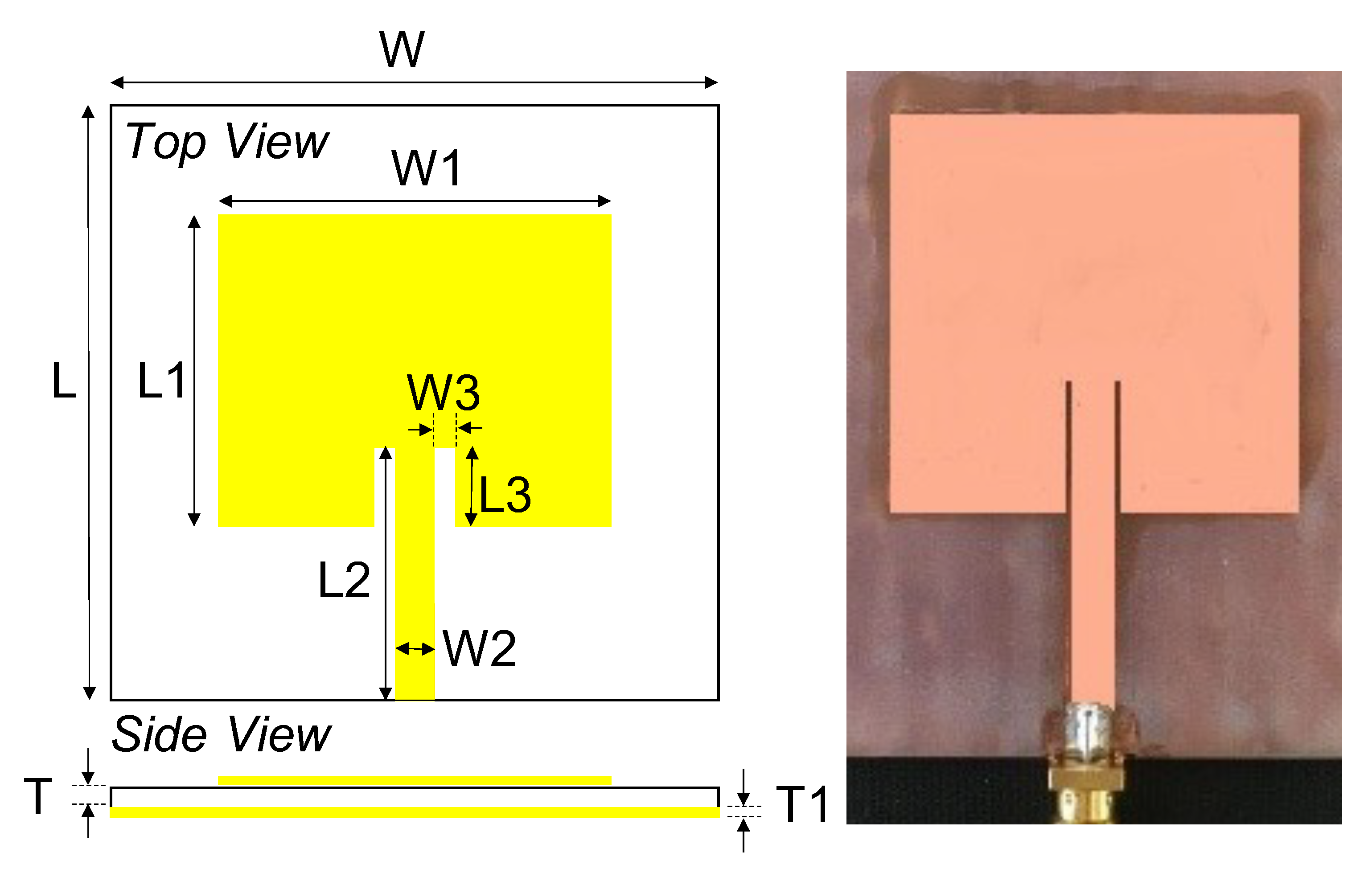
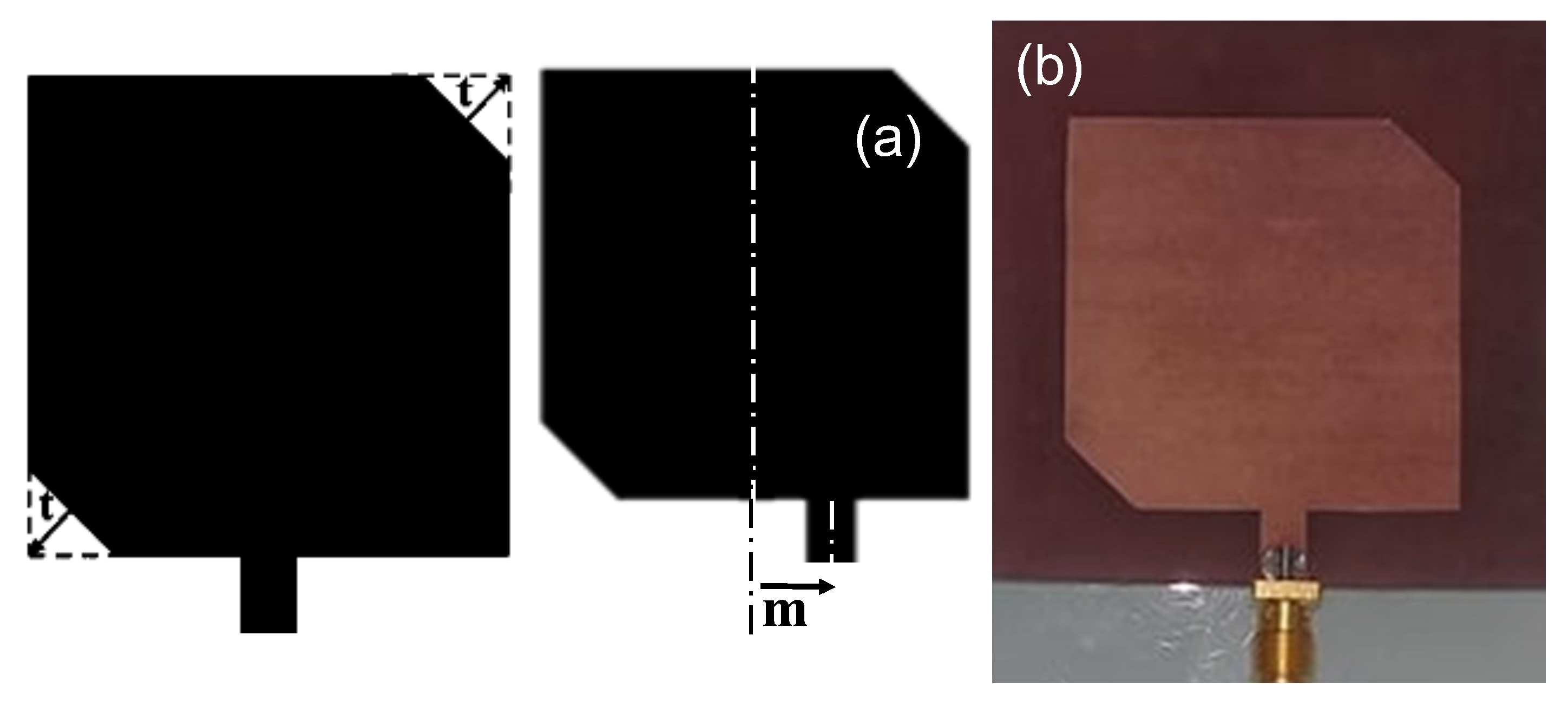
Elementary square patch antennas are designed for fabrication using the HT Resin v2 (at one point, the resin v1 was replaced by the grade v2 by the supplier). The length of the antenna is 36 mm for a resonant frequency of 2.45 GHz. A 50 micro-strip transmission line is placed on one side of the antenna, but not necessarily centered for feeding the antenna. The length of this feeding line is shortened to attenuate its effect on the radiation pattern of the antenna (consequently, the gain of the antenna).
The corners are truncated from a height, t (
Figure 3a). The feeding line is decentered of a distance, m. The gain and the axial ratio of the patch antenna are optimized through simulation to evaluate the dimension t. The reflection coefficient is affected by the feeding line position. A trade-off is defined, yielding the corner dimension, t (4.7 mm) and decentering parameter, m (+2 mm). The dimensions of the antenna in
Figure 3 are listed in
Table 4. The simulated axial ratio is 0.7 dB at 2.45 GHz. In addition, the simulated and measured realized gain of the antenna is 2.03 dB and 1.70 dB, respectively.
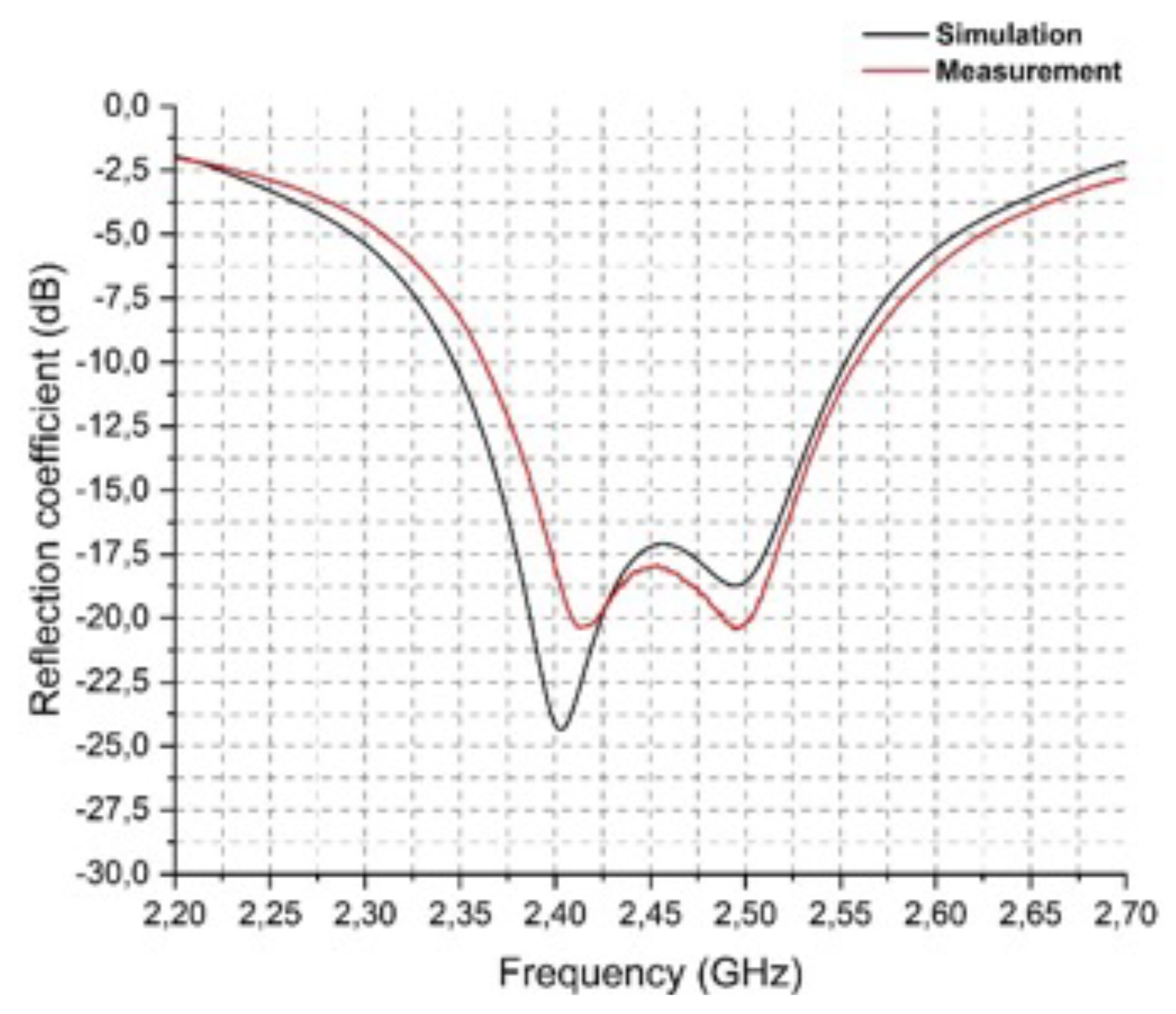
The simulated and measured reflection coefficient of the antenna in
Figure 3b is pictured in
Figure 4. The reflection coefficient is limited to −17.4 dB. It is nonetheless a satisfying value for considering an array of antennas.
The Half-Power Beam Width (HPBW) of the antenna is mentioned in
Table 5. For the previous 2D design of elementary patch antennas, the measured HPBW is around 85° in the vertical plane and 80° in the horizontal plane along the the feeding line of the antenna. The idea is then to curve the antennas with a radius in the order of
to broaden the HPBW in both planes [
61,
62]. However, the back-lobe of the radiation pattern is smaller with a larger curving radius. The author in [
63] studied the impacts of the curving radius on the performance of the circular polarization nearly-square patch antenna at 2.3 GHz. When the curving radius is approximately higher than 3
, the curvature does not affect the axial ratio of the patch antenna. The flexibility of manufacturing (advantage of rapid prototyping) easily gives access to any geometry, such as a four, curved elementary patch antenna array, as discussed below.
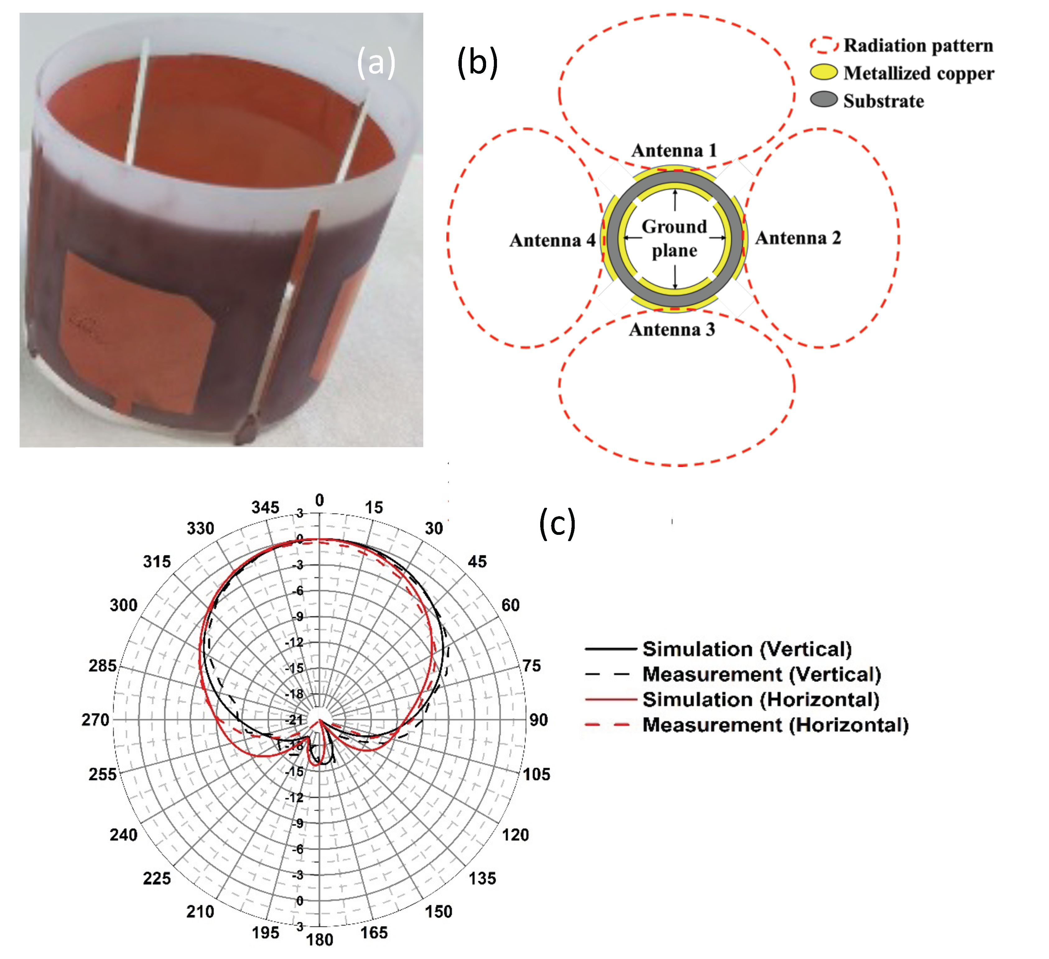
3.2. Four-Sector Antenna
A simple four-sector antenna is fabricated as a cylinder
Figure 5a with four circularly-shaped patches. The isolation between each elementary patch antenna has been simulated and measured. In
Figure 5a, the ground plane is segmented and a plane unique ground plane has also been considered. The latter option impacts negatively the isolation with −38 dB compared to −45 dB with the former option. The radiating parameters of the antennas in both considered options of the ground plane are listed in
Table 6. The matching network and the rectifier topology are then designed for the proposed antenna vehicle.
Figure 5.
Four curved elementary patch antenna array. (a) manufactured sample in HT resin V2. (b) Expected radiation pattern. (c) Radiation pattern in vertical and horizontal planes of each elementary antenna in the array.
Figure 5.
Four curved elementary patch antenna array. (a) manufactured sample in HT resin V2. (b) Expected radiation pattern. (c) Radiation pattern in vertical and horizontal planes of each elementary antenna in the array.
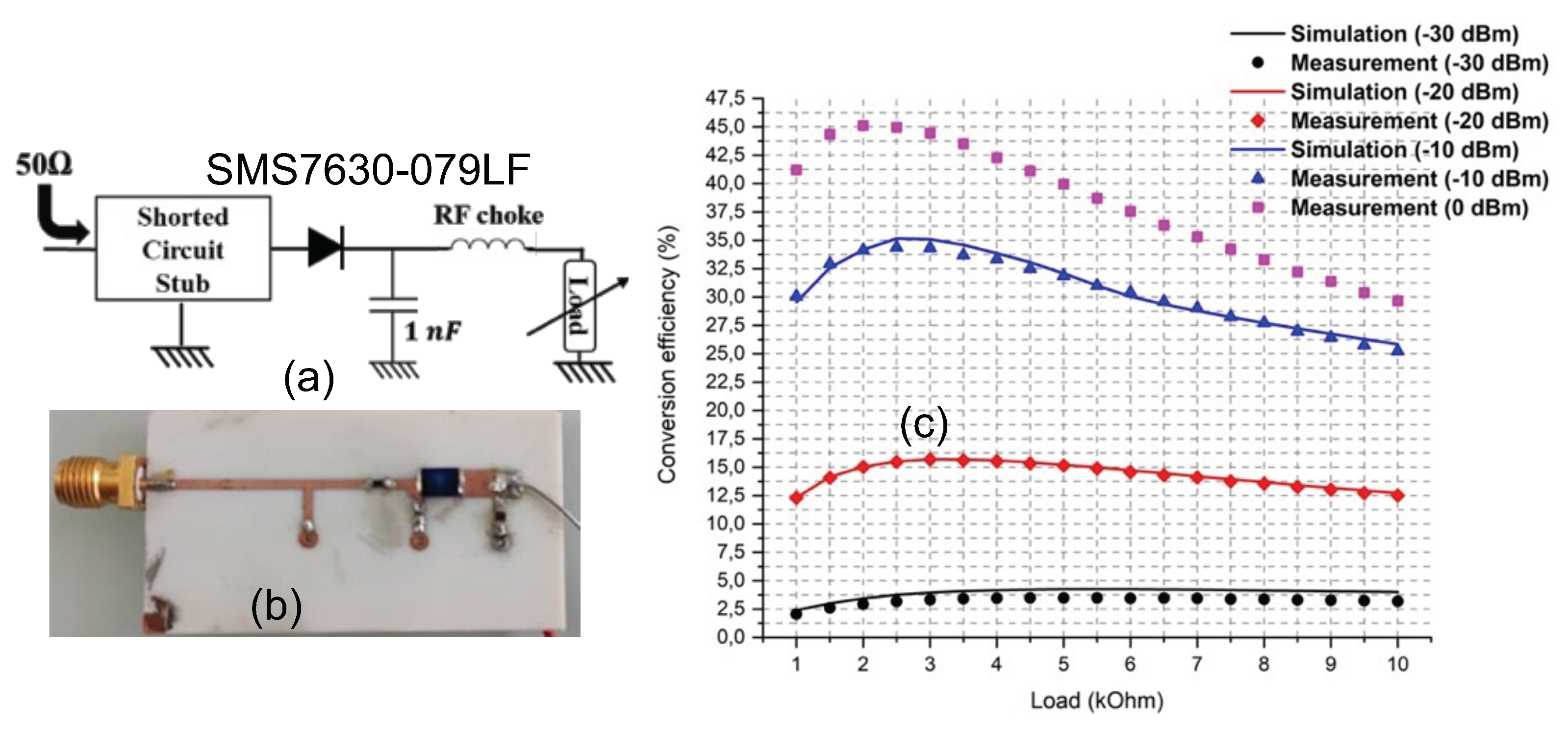
4. Rectifier and Rectenna Internal Impedance
This paper focuses on the harvesting of ambient electromagnetic energy that is very low by essence. A one-diode, series topology is selected. As mentioned in [
1] and detailed also in [
59], the diode SMS7630-079LF is a good candidate. It is worth noticing that the diode SMS7630-079LF is not as accurately modeled as the diode HSMS2850 in Keysight ADS software. The latter diode is then preferred for design purpose, but the two offered very close performances (threshold voltage, losses, reverse-bias capability).
The matching network uses micro-strip components as they are compatible with the metalization of the printed substrate and a minimal number of SMDs are then brazed on top of the conductive lines.
Figure 6b pictures a sample rectifier. The printed substrate is influencing the RF part (matching network) but not the DC-electrical part. The S
parameter of the rectifier is minimal (−28 dB) for an RF excitation of −24 dBm. The conversion efficiency is pictured in
Figure 6c for low input RF power levels. At −30 dBm input power, the conversion efficiency is 3.5% under 5 k
optimal load. This means that 350 nW are available to supply a payload, but under a voltage of 12 mV, it requires a voltage conversion to match the need of a standard CMOS circuit. This necessary circuit is detailed in
Section 5.
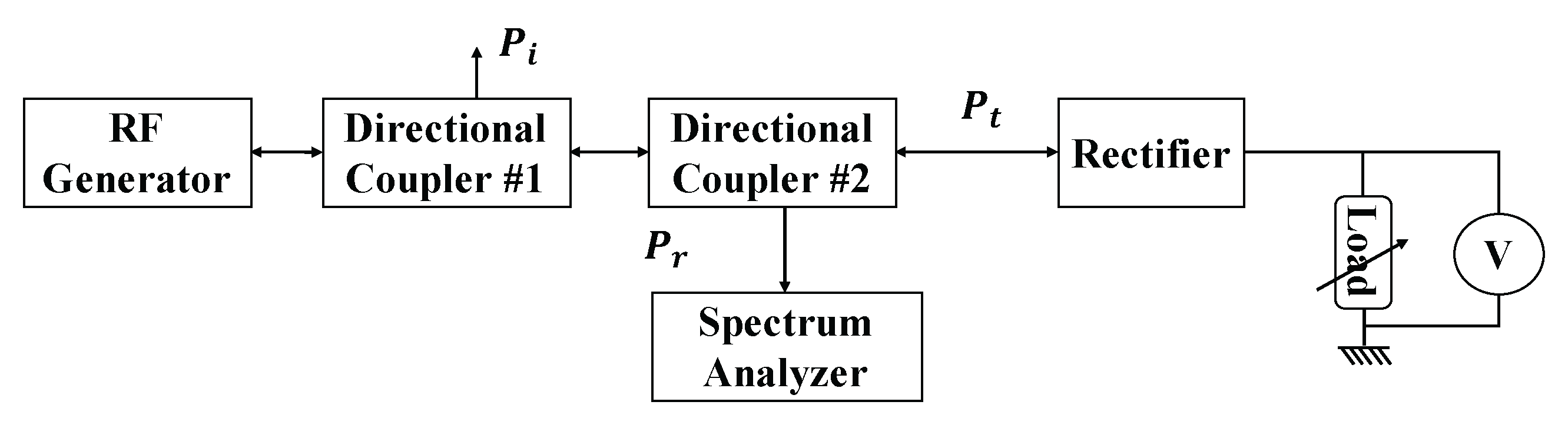
The measurements in
Figure 6c are based on a method to insure a specific input RF power level at the rectifier input, independently of the matching network adequacy with respect to the operating conditions. The setup in
Figure 7 is used for the measurements and comprises directional couplers, connectors and cables, where power losses, P
, must be identified prior to the application to the rectifier. The reflected power, P
at the rectifier input is measured to deduce the power absorbed by the rectifier input, P
. The RF generator power level, P
, is adjusted to set P
to a given and known level (namely, 0, −10, −20 and −30 dBm, respectively, in
Figure 6c). The rectifier output voltage is measured in open-circuit conditions, which implies a certain RF generator power level to obtain the targeted rectifier input RF power. The tuning is repeated for each value of the load at the output of the rectifier. The determination of the rectifier near optimal load benefits from this measurement approach, when the output voltage reaches half the open-circuit voltage value for a same input RF power level.
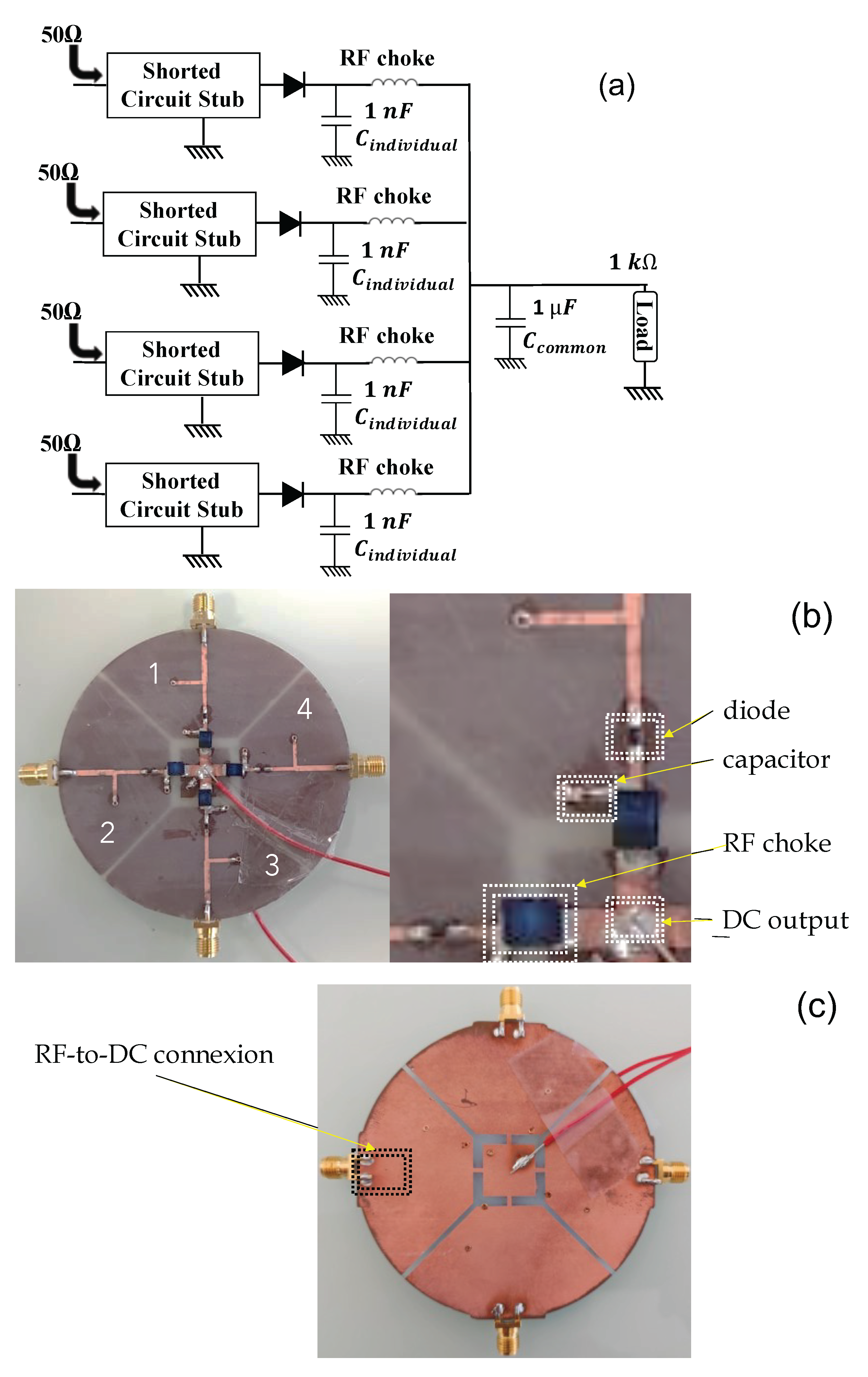
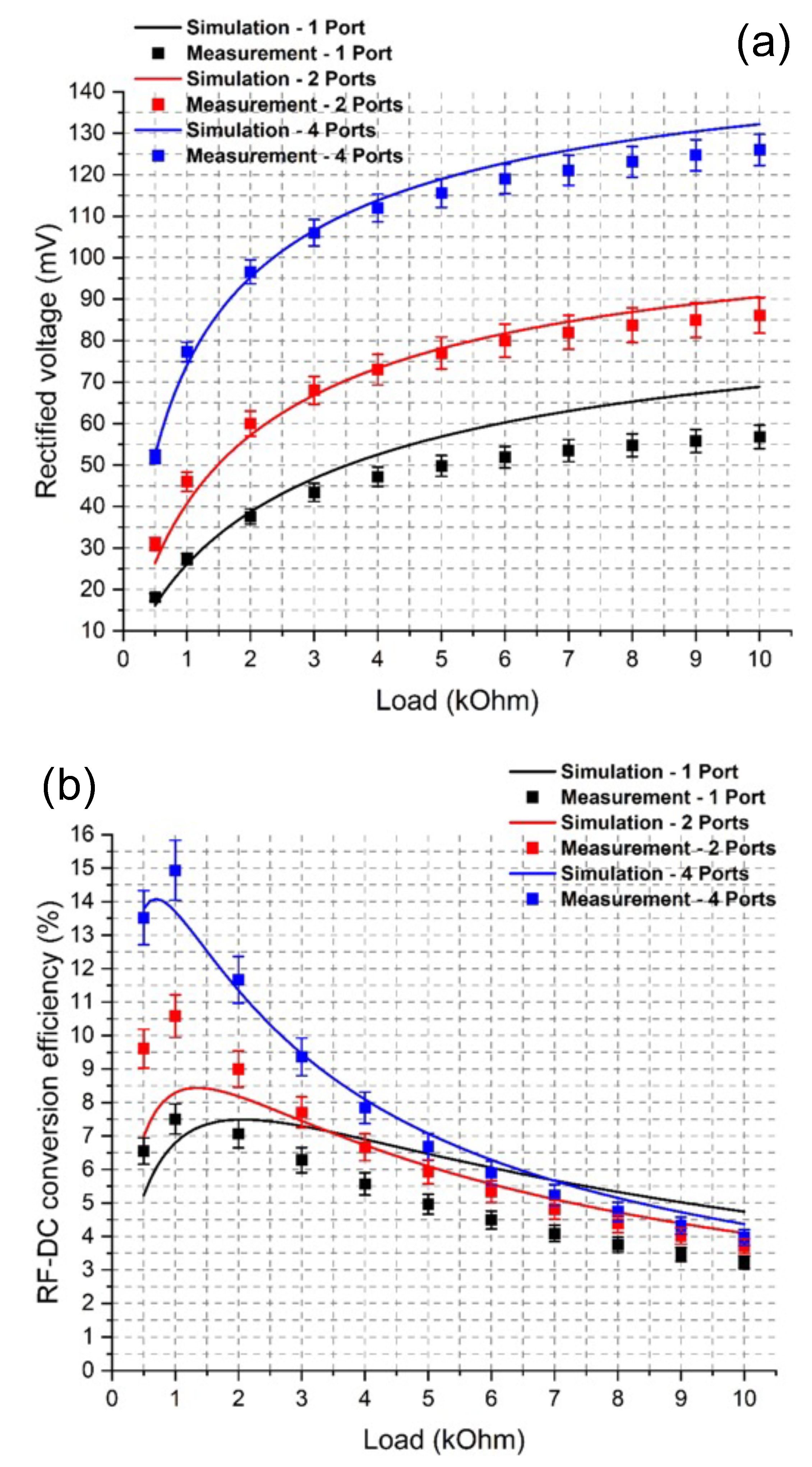
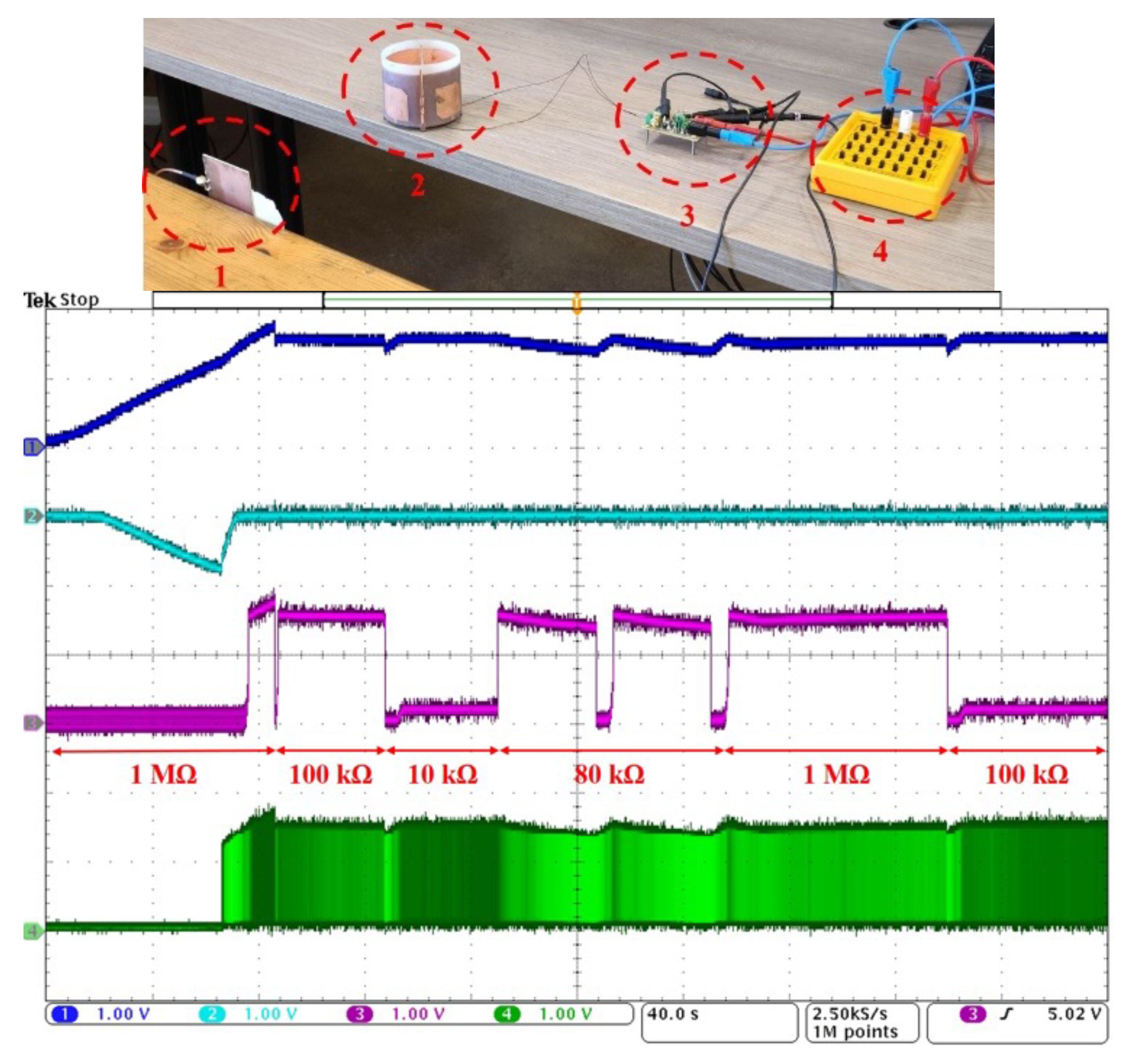
The concept of a circularly polarized patch antenna developed in the previous Section should increase the capturing of the ambient electromagnetic field and boost the conversion efficiency. One option is related to the ground plane, which can be unique or segmented by sector. The segmented ground option is preferred for the purpose of the isolation of the antennas. So, four complementary rectifiers are naturally adopted with a unique DC output (
Figure 8). It may be noted that 3D plastronic prototyping enables to fabricate exact similar portions of the rectenna circuit.
The approach in
Figure 7 is applied to characterize the open-circuit voltage and the conversion efficiency at −10 dBm input RF power and for various rectenna configurations (namely the number of antenna stimulated at the same time or the output load value). The rectifier substrate is printed in HT resin V2. In the case where two rectifier inputs are supplied simultaneously with −10 dBm and the other ports short-circuited on 50
(
Figure 9), the conversion efficiency is over 10% at an optimal load of 1.2 k
. In [
58] it appears that the internal impedance of a sector-rectenna is nearly 2010
. Unfortunately the authors do not detail how the DC paths are combined to supply a unique load. The available DC power is then 10 mW under 65 mV. A voltage conversion circuit is necessary, but the available power becomes highly compatible with IoT object power consumption.
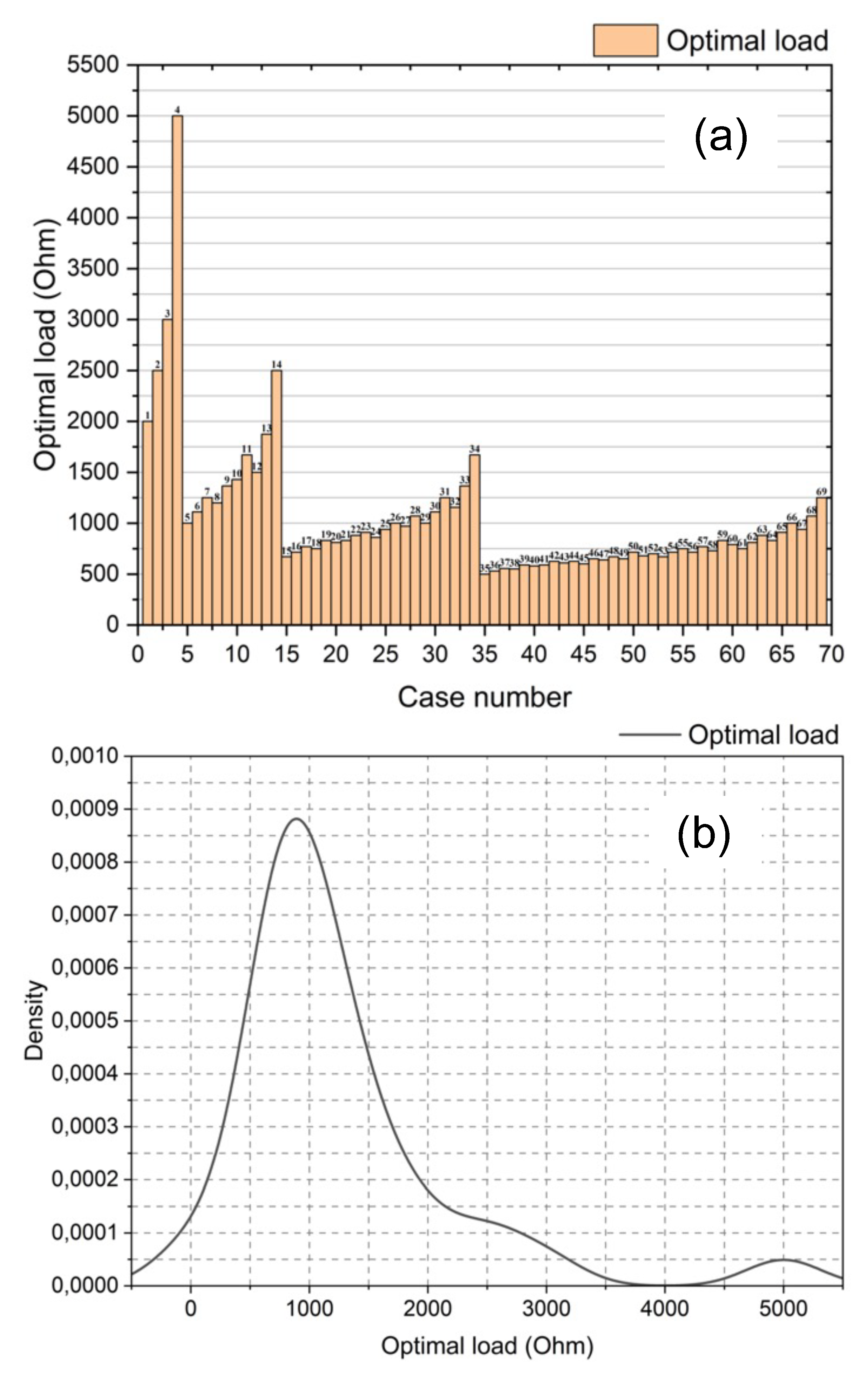
One important detail is that the excitation of the circularly polarized patch antenna by the ambient electromagnetic field is generally unknown and is varying in time. It is not reasonable to install a circuit to sense individually the DC output of each rectenna in
Figure 8 to correct the instantaneous optimal load of the system. Hence, a constant value of near-optimal load must be identified. The near-optimal load is identified in the conversion efficiency curve of the rectenna system for a given configuration of ambient electromagnetic field (i.e., which antenna is polarized and which input RF power level is applied at the related rectifier input). A Design-of-Experiment (DoE) with 69 cases is considered: the total input RF power level at the rectifier input is [−30 dBm; −20 dBm; −10 dBm and 0 dBm] and each of the 4 possible rectifier ports are considered independently (i.e., leading to cases where ports are not receiving the same input power).
The near-optimal load identification is pictured in
Figure 10. The DoE indicates that 1 k
will act as a near-optimal or closely-optimal load value in a number of cases. This value is selected as a specification for the voltage conversion block. It is clear that over time the operation of the rectenna will not be optimal in the perspective of maximum power point. There is a trade-off regarding the load value and regarding the maximum harvested energy over a time horizon.
5. Voltage Conversion Circuit
This Section details a lab-scale voltage conversion circuit that should load the rectenna with a near-optimal load of 1 k and supply an output DC load between 1.5 V and 1.9 V. As the RF power density at the antenna surface is low and lower than the energy required by an IoT sensor over an operating cycle, it is necessary to store the electrical energy.
Several commercial circuits exist to deal with the voltage conversion from energy harvesting (
Table 7). These circuits do not answer to the critical trade-off of accepting a micro-voltage source with a high internal impedance (1 k
), starting-up at the lowest possible voltage, and consuming a low bias current.
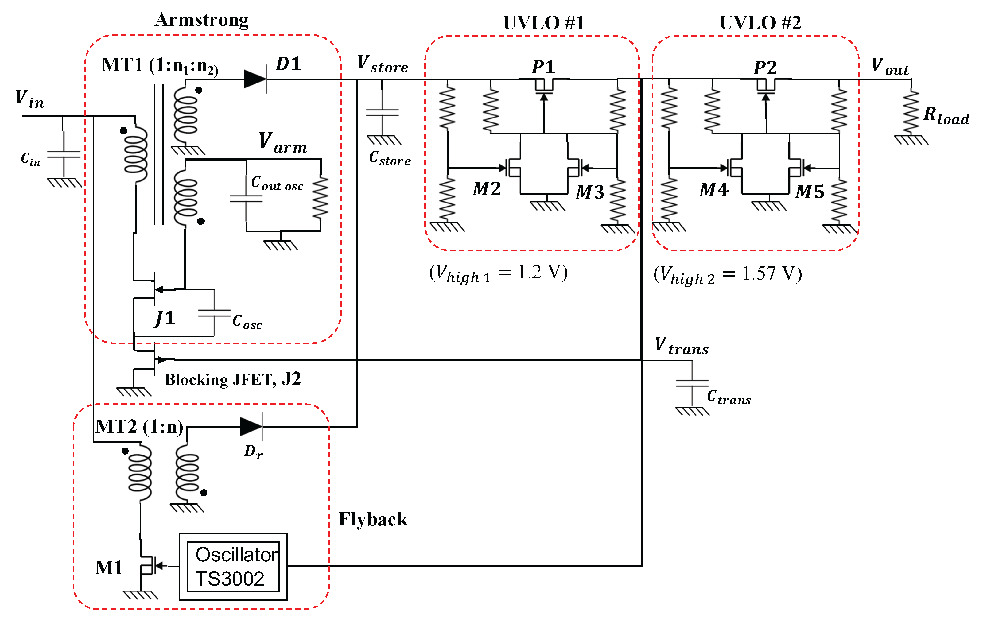
A voltage conversion circuit was proposed in [
70] to deal with the large internal impedance of the rectenna and cold-starting at the minimum voltage of 180 mV (
Figure 11). The circuit was improved in [
71] to deal with a 100
W micro-voltage source. The main converter in
Figure 11 is a Flyback DC-DC converter operating in discontinuous conduction mode (DCM). It was demonstrated in [
71] that the input impedance, R
, of the Flyback is defined in a straight-forward manner as follows:
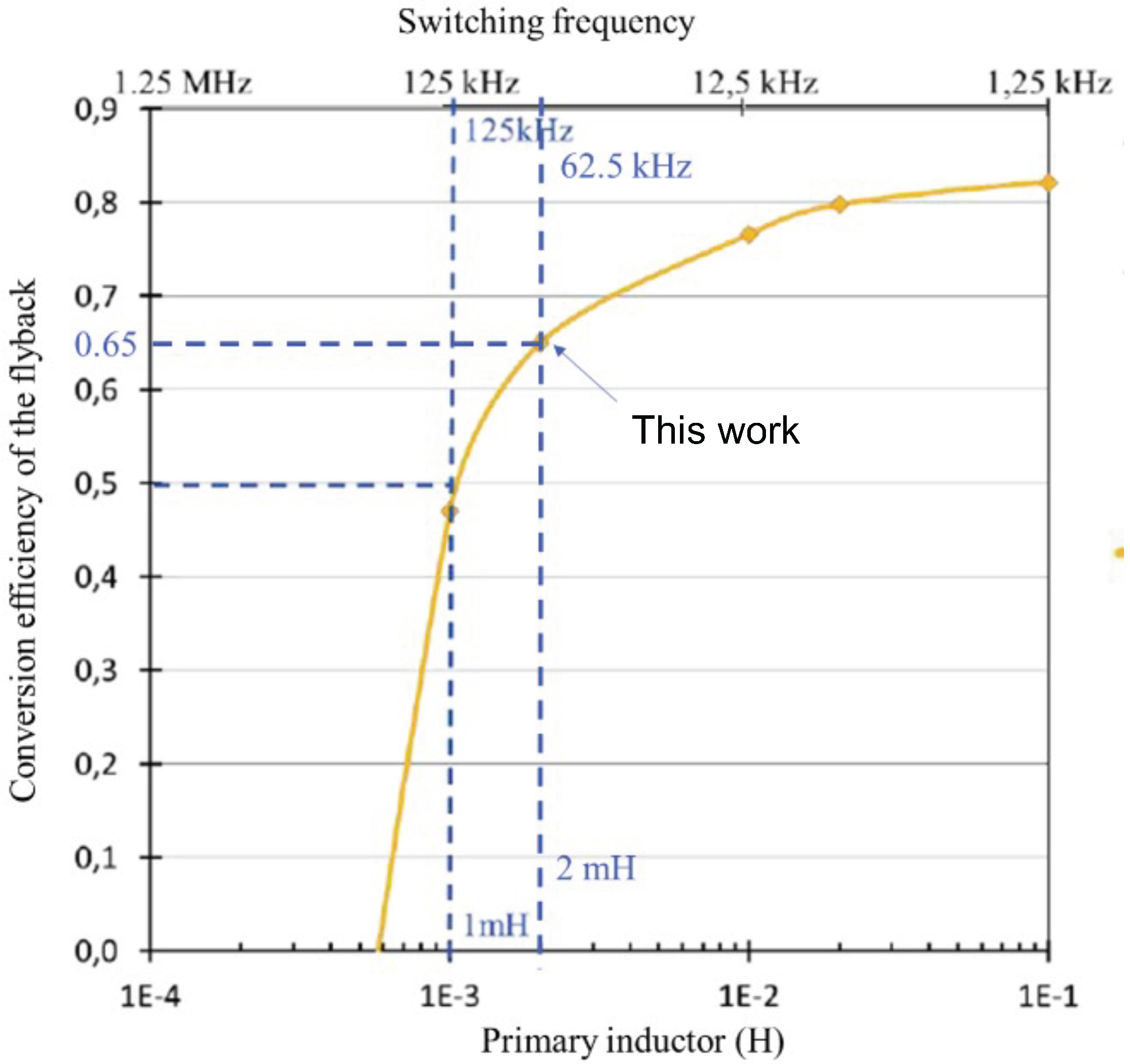
where
L is the magnetizing inductance of the coupled-inductance device,
f is the switching frequency and
d is the duty cycle (50% in most cases). Given component references and considering an ideal coupled-inductance magnetic device, it is possible to build the abacus in
Figure 12 to show the trade-off between the efficiency and the size of the magnetic device. When crossing this abacus with the commercial magnetic device offer, the designer sets the efficiency of the Flyback converter as well as its size. The size may be bulky if a large magnetizing inductance is selected with a low series resistance, i.e., a large number of winding turns with a large section conductor. Besides, popular integrated circuits in
Table 7 offer a better trade-off in terms of size, but the cold start-up voltage must be higher than the one of the lab-scale converter or the integrated maximum power-point tracking algorithm will definitely not be adapted to a RFEH. The emerging commercial circuit [
65] is one of the most appropriate offers as of today to the best knowledge of the authors, if a high integration factor is sought.
The circuit in
Figure 11 is implemented with the list of devices in
Table 8. It is verified experimentally that the Amstrong part is capable of starting-up for an input DC voltage of 180 mV. The integrated circuit LTC3108 [
66] in
Table 7 is capable of wake-up under 20 mV, but only for a low internal voltage source. This is not applicable to a RFEH.
Under −20 dBm input RF power, the rectifier delivers nearly 0.5 V in open-circuit condition. The Amstrong converter efficiency is 40.2%. It takes less than 3 s to charge a 47 F under 1.4 V. The Flyback efficiency is measured at 73% for a load of 100 k, excluding the bias current of the oscillator (TS3002). The TS3002 oscillator draws 4 J in normal operating conditions. The UVLO blocks consume a negligible energy. The net output power of the voltage conversion circuit is more than 7.2 W at −20 dBm input RF power. It will then take nearly 14 s to store 100 J in the output capacitive buffer. As will be discussed later on, supplying an IoT sensor will lead to a sporadic operation if the IoT’s consumption is too high or the input RF power drops in level and the Flyback cannot operate any further. The Flyback is able to operate with an input DC voltage as low as 100 mV, i.e., 10 W.


 ,
, 


