Article

Decoding Algorithms and HW Strategies to Mitigate Uncertainties in a PCM-Based Analog Encoder for Compressed Sensing

1
Department of Electronics and Telecommunications, Politecnico di Torino, 10129 Torino, Italy
2
“Ercole De Castro” Research Centre on Electronic Systems for Information and Communication Technologies, University of Bologna, 40126 Bologna, Italy
3
Department of Electrical, Electronic, and Information Engineering “Guglielmo Marconi”, University of Bologna, 40126 Bologna, Italy
4
Computer, Electrical and Mathematical Sciences and Engineering (CEMSE), King Abdullah University of Science and Technology (KAUST), Thuwal 23955-6900, Saudi Arabia
5
STMicroelectronics, 20864 Agrate Brianza, Italy
*
Authors to whom correspondence should be addressed.
J. Low Power Electron. Appl. 2023, 13(1), 17; https://doi.org/10.3390/jlpea13010017
Submission received: 30 November 2022 / Revised: 6 February 2023 / Accepted: 9 February 2023 / Published: 13 February 2023

Abstract

:
Analog In-Memory computing (AIMC) is a novel paradigm looking for solutions to prevent the unnecessary transfer of data by distributing computation within memory elements. One such operation is matrix-vector multiplication (MVM), a workhorse of many fields ranging from linear regression to Deep Learning. The same concept can be readily applied to the encoding stage in Compressed Sensing (CS) systems, where an MVM operation maps input signals into compressed measurements. With a focus on an encoder built on top of a Phase-Change Memory (PCM) AIMC platform, the effects of device non-idealities, namely programming spread and drift over time, are observed in terms of the reconstruction quality obtained for synthetic signals, sparse in the Discrete Cosine Transform (DCT) domain. PCM devices are simulated using statistical models summarizing the properties experimentally observed in an AIMC prototype, designed in a 90 nm STMicroelectronics technology. Different families of decoders are tested, and tradeoffs in terms of encoding energy are analyzed. Furthermore, the benefits of a hardware drift compensation strategy are also observed, highlighting its necessity to prevent the need for a complete reprogramming of the entire analog array. The results show >30 dB average reconstruction quality for mid-range conductances and a suitably selected decoder right after programming. Additionally, the hardware drift compensation strategy enables robust performance even when different drift conditions are tested.

1. Introduction

Computations must be performed as close as possible to where data are located. This is a request emerging nowadays from all those fields characterized by the processing of a large amount of data, especially if low latency and low power consumption are required. All these needs could make the performance of classical von Neumann architectures insufficient. The main limitation of such systems is the communication bottleneck, i.e., data must be moved to the processing unit and the computed output must be moved back to the memory [1,2].
Overcoming this limitation is the main goal of the novel computational approach, commonly named In-Memory Computing (IMC). A widely investigated approach for IMC is represented by the Analog In-Memory Computing (AIMC) in which resistive memory devices act as a non-von Neumann architecture performing matrix-vector multiplication (MVM) where the matrix coefficients are stored [3]. Embedding MVMs in memory devices could be a revolutionary innovation in several fields ranging from machine learning applications [3,4,5] to data compression [6,7]. The idea underlying the computation of MVMs in AIMC is to leverage Ohm’s and Kirchhoff’s laws [2,8,9]. However, care must be taken as the results are affected by the non-idealities of these families of devices.
Among the most employed technologies for NVMs, Static Random Access Memory (SRAM), Phase-Change Memory (PCM) and Resistive Random Access Memory (RRAM) represent valid candidates to be employed in the AIMC framework. In SRAM, the information is stored in the form of electric charge, with almost unlimited cycling endurance and sub-nanosecond reading and writing access times [10,11]. PCM technology, which exploits the resistivity transition of phase-change materials, is a solution that promises multi-level programming and long-term storage capabilities [12,13]. High speed, high scalability, low power consumption and CMOS compatibility are also granted by RRAM and MRAM devices [14,15]. AIMC features have also been implemented using non-volatile Spin–Orbit Torque (SOT) memory devices [16] and Dynamic Random Access Memory (DRAM) cells [17]. The effects of the non-idealities affecting each device technology directly impact the performance of AIMC architectures. Indeed, a transversal research effort was directed to the solution of such challenges across several abstraction levels.
This work focuses on the applicability of PCM technology. For this class of devices, the non-idealities affecting the output of MVMs are: (i) a nonlinear dependency between the input voltage and the output current of a PCM cell, i.e., a nonlinear I-V characteristic; (ii) a degradation over time of the conductance value stored in each cell, i.e., the conductance drift; and (iii) variability in the programmed conductance value, i.e., the programming variability [18]. For what concerns the nonlinear I-V characteristic, a common solution has been proposed in the literature [4,19,20,21]: instead of representing input values as voltage levels, a constant voltage is applied across each cell for a time that is proportional to the desired input value. Conversely, conductance drift can be partially compensated by post-processing approaches modeling the average behavior [4] or by means of HW-aware training solutions [22] in case of neural network applications or having dedicated architectures [21]. To reduce the impact of the programming variability, the effort is in the identification of program-and-verify algorithms [5,23]. A detailed analysis of memory array non-idealities was conducted in [24,25]. At the same time, significant progress has been made in the development of compact models of PCM device behavior [26]. As a final remark, let us stress that all presented solutions for the conductance drift and the programming variability only mitigate these non-idealities.
Having a target application, systems embedding PCM devices must be properly designed with the goal of preserving their intrinsic advantages and reducing the effects of their non-idealities to the greatest extent. In this work, we focus on the design of a low-power data compression system adopting the Compressed Sensing (CS) framework [27]. In this paradigm, the encoder only requires a matrix multiplication between the vector containing the data to be compressed and a properly designed wide matrix named sensing matrix. The multiplication between the two produces a vector, named measurement vector, with less entries than the original one. This light compression mechanism includes a decoder that, knowing the adopted sensing matrix, recovers the original vector by only accessing the measurement vector and solving an optimization problem [28]. A large variety of decoding approaches have been presented in the literature [29,30,31,32,33], operating within different theoretical frameworks. In any case, the nonlinear decoding stage represents the largest drawback for a CS-based signal chain and leads to sub-par performance in real applications if compared with more traditional acquisition and compression schemes. Its use is only justified in practice if encoding energy efficiency is a concern.
Here, we analyze hardware and software solutions that could make the adoption of PCM cells in the design of a CS encoder more effective. Results are supported by tests carried out on an AIMC unit testchip [21]. This prototype was implemented in a 90 nm STMicroelectronics CMOS technology and includes a circuit-level solution to reduce the PCM cells conductance drift. The effect of programming variability and the residual drift are analyzed by comparing the performances of different families of CS decoders.
The analysis will identify, among others, a trade-off between encoding energy and reconstructed signal quality. Indeed, different works have focused on the exploration of the design space for CS acquisition chains, associating the system parameters with the desired quality for a specific application. As an example in the context of ECG signal acquisition, a dual-mode ECG monitor is presented in [34], where an appropriate compression level is selected based on the different quality requirements (heart-rate detection vs. medical grade ECG traces). A more general analysis is performed in [35], identifying 21 dB and 34 dB as thresholds for a “good” and “very good” ECG trace, respectively. The present analysis involves synthetic signals in the Discrete Cosine Transform (DCT) domain, and considers an encoding-energy/reconstruction quality trade-off, simultaneously observing the robustness against conductance drift introduced by a hardware compensation strategy.
The paper is organized as follows. In Section 2, the architecture of the employed testchip is recalled, and numerical models are presented describing the statistical features of programming variability and conductance drift. The theoretical framework of Compressed Sensing is introduced in Section 3, and the experimental results are analyzed in Section 4. Finally, the conclusions are drawn.

2. AIMC Testchip and Conductance Models

This section summarizes the features of the AIMC testchip used to perform one-step signed Multiply-and-Accumulate (MAC) operations (which implement MVMs), and presents the PCM devices’ conductance variability model exploited in simulations.

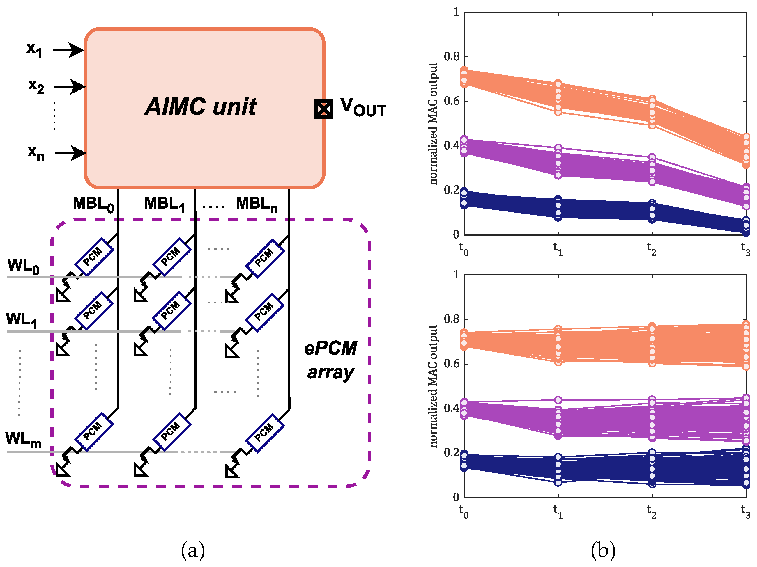
2.1. AIMC Testchip Structure

The AIMC testchip includes a peripheral AIMC unit interfaced with an embedded PCM (ePCM) IP [36]. While the ePCM stores the MAC coefficients, the AIMC unit performs the whole operation in an analog fashion reading the ePCM cells currents. A more detailed description of the architecture, as well as the interface between AIMC unit and ePCM, can be found in [21]. The entire testchip is manufactured in a 90 nm STMicroelectronics CMOS technology, which features a specifically optimized Ge-rich GeSbTe (GST) alloy for PCM cells. The testchip is conceived to extend the ePCM IP functionalities by adding MAC execution features to the standard binary use. Furthermore, the AIMC unit architecture is designed to mitigate the effect of the conductance drift of the PCM cells to the accuracy of the operation.
The MAC execution feature is obtained by exploiting the AIMC peripheral unit which is connected to the main bit lines (MBLs) of the ePCM IP, as depicted in Figure 1a. The AIMC unit takes as input a vector  x = [ x 1 , , x n ]  and executes the MAC operation  x · g j , where  g j = [ g j 1 , , g j n ]  are the conductances stored in the j-th word line (WL). To this purpose, the AIMC unit applies a read voltage  V REF  on each MBL and reads the currents of the cells for the selected WL. The result of the operation is mapped on a voltage value by integrating the sum of the cells’ currents for an interval  T MAC . Each single cell current  I i = g i V REF  is integrated for a time window  T ON i  which is proportional to the corresponding input  x i . Accordingly, the expression of the output  V OUT j  at the end of the integration window is:
V OUT j = k i = 1 n ± g j i g REF V i ,
where  g j , i  is the conductance of the PCM cell representing an element of the vector stored in the j-th row of the array,  g R E F  is the conductance of the reference PCM cell,  V i  is the analog voltage level of the input vector element  x i , and k is a dimensionless constant value accounting for the effects of circuit parameters. The drift compensation technique adopted in this prototype exploits the proportionality of the MAC result to the conductance ratio  g j i / g R E F . Indeed, the drift of a generic cell conductance has been proven to follow the power law [37]:
g ( t ) = g 0 t t 0 α ,
where  g 0  is the conductance at an arbitrary initial time  t 0 , and  α  is the device drift coefficient, which is positive and cell-to-cell variable. The drift coefficient of the ratio  g j i / g REF  is therefore reduced to  ( α j i α R E F ) , so that its drift is partially compensated. At the circuit level, to compensate the drop in value of the stored conductances, the  g REF  conductance modulates the value of each  T ON i  according to its own drift [21].
The performance of the drift compensation technique adopted in this prototype can be observed in the experimental results shown in Figure 1b, where a set of 450 cells has been programmed with a dedicated iterative algorithm [23] with three different target conductance levels  g T  with a normalized tolerance  Δ = 0.05 . Then, the single weights  g j i / g REF  have been observed setting all but the i-th inputs to 0, whereas  x i  was chosen equal to its maximum value. This operation was repeated for all 450 cells after 2 and 18 h from the programming time. Then, the prototype was baked for 24 h at 90  C  in a controlled climate chamber to accelerate the cells’ drift phenomena [38] and measurements were repeated at room temperature. The selected setups enable the testing of the compensation strategy under the effect of severe drift, highlighting how circuit performance can be preserved by its use. In the top plot of Figure 1b, a constant test conductance was employed as  g REF  (i.e., no drift compensation was adopted), whereas the bottom plot shows the effect of using a drifting PCM device as a reference cell, highlighting its beneficial effect on the cell set evolution.

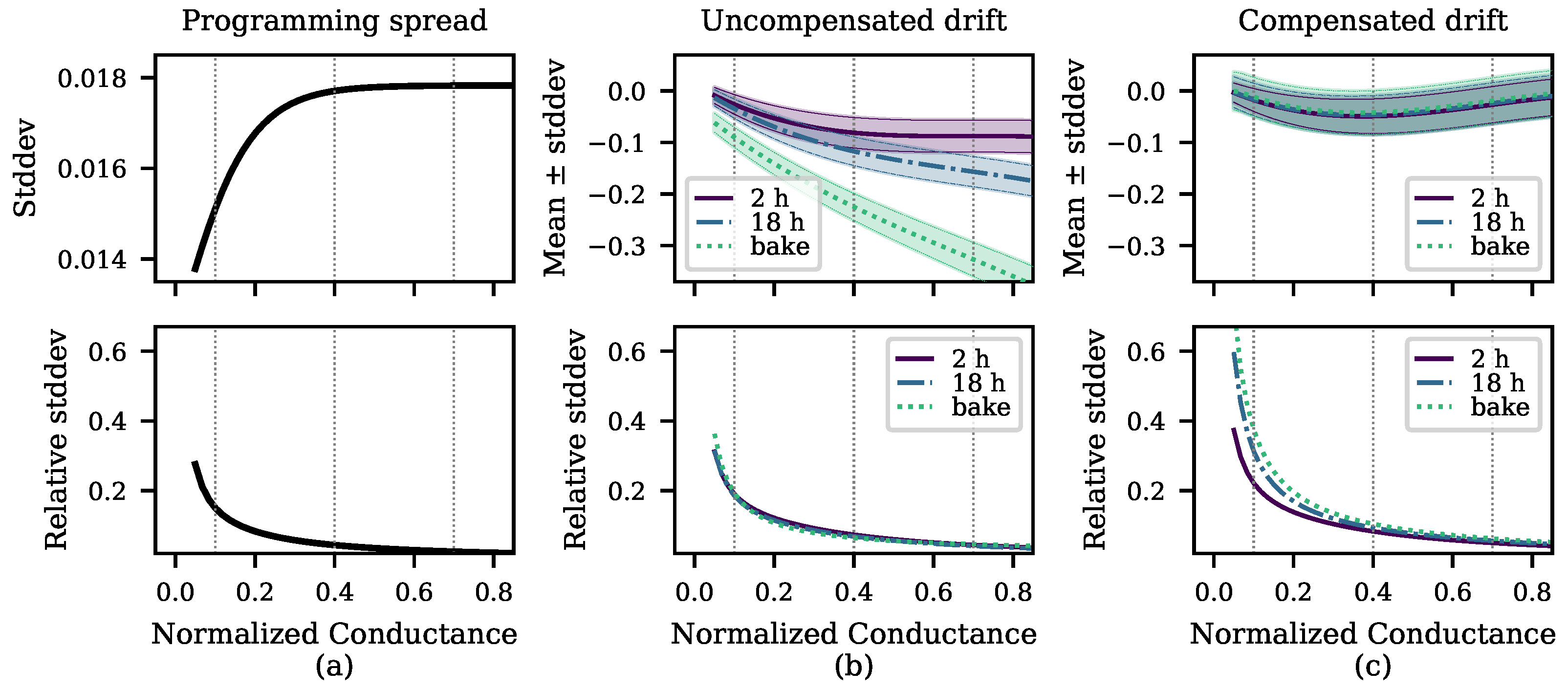
2.2. Modeling the Conductance Variability

Using the approach proposed in [39] as a reference, numerical models describing both the programming variability and the conductance drift over time have been constructed from a larger set of measurements, collected for 32 different target conductances. The algorithm employed to program each PCM cell has been proposed in [23], and it is conceived to grant a large number of programmable values with a SET-Staircase (SSC) pulse sequence, as well as reduce the effect of drift through the application of appropriate high-amplitude SET and RESET pulses at the beginning of the programming procedure. The batches of devices, programmed to different target conductances, have been characterized immediately after programming and then following the drift-induced variations. Statistical summaries of the relevant quantities were been computed, namely the standard deviation of the programming spread and both the mean and standard deviations for the drift-induced conductance difference  g ( t ) g ( t 0 ) .
Figure 2 shows numerical fits of the statistical summaries, over the available (normalized) conductance range. Standard deviations, both for the programmed conductances and the drift-induced spread, are described by
σ ( g ) = σ 0 + σ 1 tanh ( g / γ 0 ) .
Conversely, the mean drift  μ ( g )  trend was described by polynomials of degree 3. A least squares fit using the Levenberg–Marquardt algorithm was used to find the parameters  σ 0 σ 1  and  γ 0  and the polynomial coefficients for each one of the four setups (after programming, and after 2, 18 h and after additional 24 h bake) being considered (as in [39]).
The programming spread shows an initial growth trend, saturating in the right-half of the domain. The upper bound on the spread is implicitly enforced by the programming algorithm, which ensures that the conductances will lie within the specified distance  Δ  from the target value  g T , and hence, the saturated behavior observed in Figure 2a. Conversely, the bottom plot of Figure 2a highlights how the decrease in standard deviation does not balance the decrease in nominal target conductance leading to an increase in their ratio.
The drift data in Figure 2b,c show how the hardware compensation obtained by the introduction of the conductance ratio  g j i / g REF  is able to significantly reduce the mean component of the drift by up to one order of magnitude, at the cost of a wider spread. For the models to be truly reliable and representative of the properties of the technology, the characterization should be extended across different chips, temperatures and operating conditions. The limited data currently available give hints towards the performance obtainable under the considered test setup.

3. Compressed Sensing Reconstruction

Compressed Sensing [40,41] is a technique that combines both signal acquisition and compression through low-complexity linear encoding that can be represented by a matrix-vector product. The incurred cost is a complex decoding phase, which requires the solution of minimization problem to recover the original signal. For it to be applicable, CS requires the n-dimensional signal  x R n  to be sparse in a suitable vector space, with basis  D R n × n . The representation of x under D ξ R n , with  ξ = D T x , is k-sparse if only  k n  of its values are significantly non-null. The acquisition procedure requires the computation of m measurements,  y 1 , , y m , with  m n , such that:
y j = i = 1 n a j i x j ( j = 1 , , m ) ,
with  a j i  suitable weights. In matrix form, the encoding operation becomes:
y = A x ,
where  A = [ a j i ]  is called the sensing or acquisition matrix.
General results exist with the possibility of exact signal recovery [28,40], prescribing the solution of a non-convex minimization problem that looks for the sparsest  x ^  that generates the observed measurements y:
x ^ = D · argmin ξ | ξ | 0 s . t . A D ξ = y .
where  | · | 0  is the  0  pseudonorm counting the number of nonzero elements in its argument. Although the general theory of CS was developed for sensing matrices with Gaussian i.i.d. entries, it has been shown [42] that negligible performance degradation incurs when sub-Gaussian distributions are applied, having only few discrete levels.

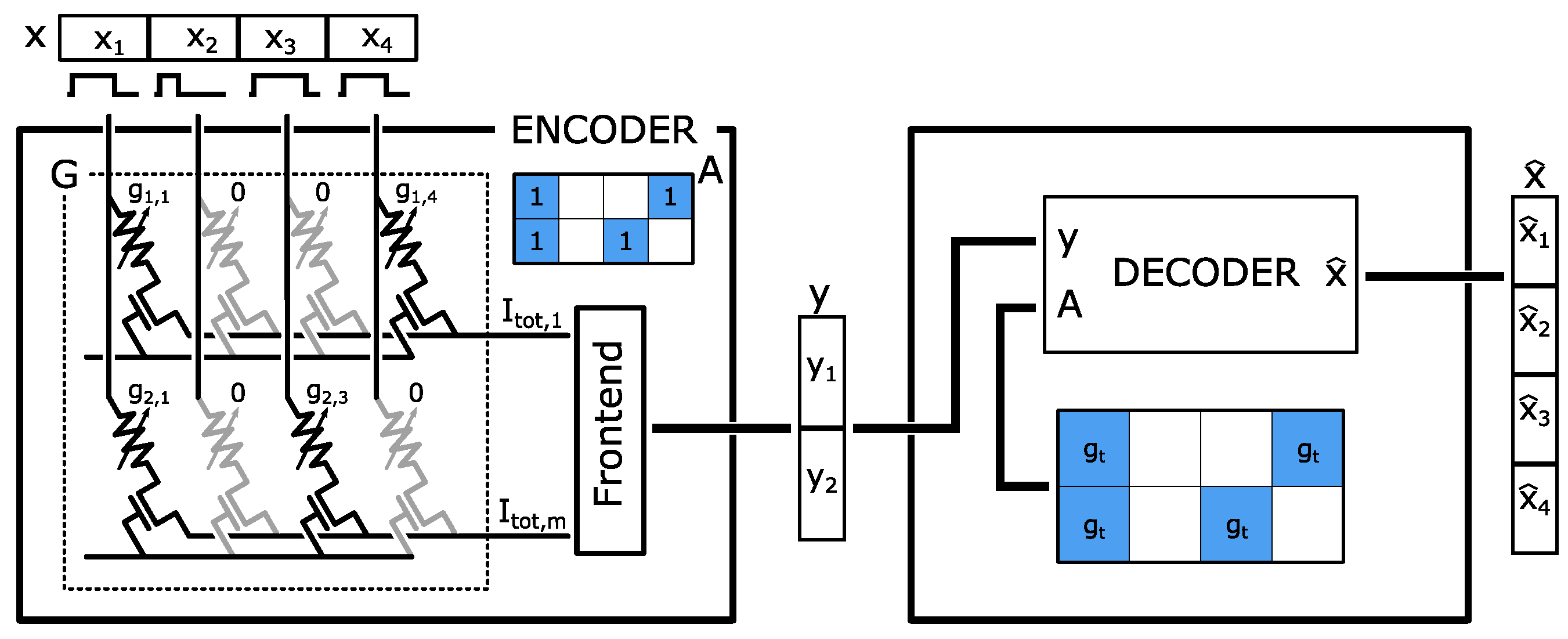
3.1. Acquisition Matrix Implementation

In general, the correct reconstruction of the original signal requires the exact knowledge of y and A. In reality, however, y will be corrupted by noise, so that the encoder output will be  y + ϵ . Moreover, the sensing matrix weights, as implemented in a PCM-based encoder, will show both programming variability and conductance drift. In the following, we will mainly be concerned with the issues caused by an uncertain A, neglecting additional noise terms on the signals. In this work only binary matrices will be used, whose entries are either 0 or 1. The two states are mapped to the low conductivity (RESET) and the high conductivity (SET) states of the PCM cells, respectively, so that a direct relationship between the PCM implementation of the sensing matrix and reconstruction accuracy obtained by the different decoder algorithms can be investigated.
Let us refer to the physical implementation of the ideal sensing matrix A as  G = [ g j i ] , as shown in Figure 3. Zeroes in A will be implemented by PCM cells in the RESET state (i.e., the most resistive state), for which it is reasonable to assume that  g j i = 0 , (i.e., an ideal zero). This assumption is motivated by the ability to program cells in RESET state, whose conductance can be several orders of magnitude below the SET state [19]. Conversely, the nonzero values in A are represented by PCMs in a properly selected SET state, such that
g j i = g T + Δ g p + Δ g d ( Δ t ) ,
where  Δ g p  and  Δ g d  are the programming and drift-induced variabilities, respectively, and  g T  is the nominal target conductance. The programming variability is a zero-mean normal distribution whose standard deviation  σ p ( g )  is the one depicted in Figure 2a and described by (3). The drift term is instead a Gaussian with a mean value  μ d ( g , Δ t )  and a standard deviation of  σ d ( g , Δ t ) , as shown in Figure 2b for the solution without drift compensation, and in Figure 2c when using drift compensation. The mean component is a degree-3 polynomial function of the input, while the standard deviation is still described by (3), although using a different set of parameters. In accordance with the experimental behavior of the employed PCM cells of Figure 2b,c, both the mean value and standard deviation of  Δ g d  depend on the cell initial conductance g and on the considered time interval  Δ t  after the programming procedure.

3.2. Reconstruction Algorithms

A wide variety of techniques have been proposed for the solution of the optimization problem in (6). A brief introduction on the algorithms employed in this work is given here.
SPGL1 [29] solves the basis pursuit denoising problem by recasting it as a root-finding for an equivalent nonlinear equation. In doing so, it administers the trade-off between the least-squares fit characterizing the constraints in (6) and the  | ξ | 1  as an alternative objective function representing a good proxy of the sparsity-level of  ξ .
The Orthogonal Matching Pursuit (OMP) is a greedy, iterative algorithm for sparse approximation. At each iteration, it looks for the component of the product  A D  which best explains the measurements. Given a sparsity-level k for the family of input signals being acquired, it completes at most k iterations, making it extremely fast. The variant used in this work is the generalized OMP (GOMP), which selects more than one vector in each iteration, thus reducing the computational complexity and making the decoder more robust to measurement non-idealities [31].
Generalized Approximate Message Passing (GAMP) is based on the concept of Belief Propagation, whereby the posterior distribution for each  ξ i  is updated based on the observations. This allows flexibility in the selection of prior models on both x and the measurement process. In the case of the uniform standard deviation of the sensing matrix weights A, it performs at a level comparable to its variants specifically designed to manage sensing matrix uncertainties [33], and hence relies on its non-specialized implementation.
Although, SPGL1 is designed to find the optimal solution for (6), we expect lower performances if compared with those that could be obtained by means of both GOMP and GAMP since they possess the capabilities to manage the sources of non-idealities in the computation of y.

4. Experimental Validation

A simulated performance evaluation, based on the experimental results of Section 2, was run on 1000 signal instances, sparse in the Discrete Cosine Transform basis, with  n = 256 k = 26  and a high-pass spectral profile, and 1000 binary sensing matrices, with  20 %  nonzero elements. A compression ratio equal to 2 was selected, consequently,  m = 128 . The performance metric considered is the Reconstruction SNR (RSNR), defined as:
RSNR = SNR ( x , x ^ ) = 20 log x 2 x x ^ 2
Each decoder requires knowledge of the sensing matrix being applied to the input at the encoder. However, in accordance with (7), the only information truly available is the target conductances  g T  used to implement the nonzero elements of A. Here, we consider also having reliable information on the mean component of the drift  μ d ( g , Δ t ) , as a result of the application of the hardware compensation scheme presented in Section 2. This additional information is provided to the decoder to explore the performance obtained after some time from the original programming of the analog array. A more general characterization of the drift effect (i.e., without considering any compensation technique) would require the inclusion of additional information to be provided to the decoder, such as PCM device technology, chip-to-chip variations and real-time working temperature, whose effects can be attenuated through the implementation of the compensation scheme. The hardware compensation is therefore expected to provide a more robust and extensive model of the drift phenomena.
Conversely, the reconstructor is unaware of the individual spread introduced by both the programming procedure and drift-induced spreads. As a consequence, each element in a given realization of the sensing matrix used at the decoder is identical, being either a true zero or a conductance  g T  whose value has drifted over time by means of an estimation of  μ d ( g T , Δ t ) .
All algorithms were tested in a Python environment, using the spgl1 (https://spgl1.readthedocs.io/en/latest/ (accessed on 30 November 2022)), and magni [43] libraries, the latter including an implementation of the GAMP decoder. The GOMP algorithm was constructed from an existing implementation of OMP (https://github.com/davebiagioni/pyomp (accessed on 30 November 2022)). The SPGL1 decoder requires a parameter  σ  representing the expected measurement error. For each target conductance being tested,  σ  was computed by encoding a batch of inputs with the perturbed and ideal sensing matrices, computing the norm of the difference and then averaging across the batch. The GAMP decoder instead requires an estimate of the input channel properties, namely the mean and variance of the nonzero components in the sparse representation of the inputs. Moreover, an estimate of the variance of the measurement noise is needed for the output channel model.
To explore the trade-offs involved in a PCM-based CS system, both in terms of performance and energy consumption, three normalized target conductances were selected, namely 0.1, 0.4 and 0.7, to represent the nonzero values in the binary matrix. These values, which are highlighted in Figure 2 as vertical dotted lines, have been identified to highlight the different behavior of low-, medium- or high-conductances, observing the trade-off to be managed in the entirety of the available conductance range. At the lowest conductance, one observes the smallest programming spread, as well as small variability induced by the drift. However, in relative terms, this represents the worst case scenario. Conversely, at the highest conductance, PCM devices show the best properties, in terms of relative spread, at the cost of an increased energy consumption, both in the programming phase and in the computation procedure.

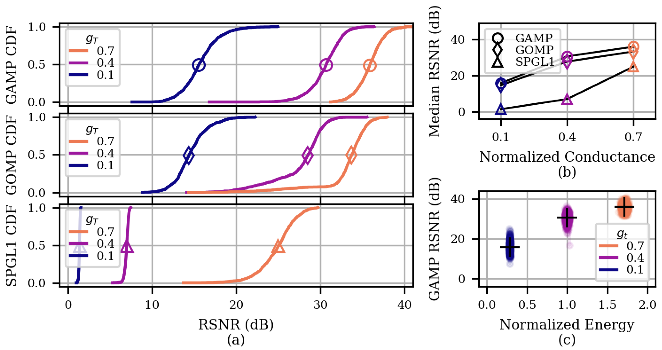
4.1. Effects of the Programming Variability

Firstly, the reconstruction performance is evaluated considering the programmed PCM cells in  t 0 . Hence, the nonzero elements in G are implemented by
g j i = g T + Δ g p ( g T ) ,
with the decoder only being aware of the nominal value  g T .
The behavior of the relative standard deviation of the programming spread immediately maps to the reconstruction performance observed in Figure 4a for the three target conductances being tested. Increasing  g T  decreases the spread in relative terms and leads to better performance, although with increasingly less benefits, as summarized in Figure 4b.
From the standpoint of the reconstruction algorithms, GAMP is the most suitable decoder under any circumstance. Strikingly, the performance of GOMP, which is unaware of the properties of the input or output channels, is extremely close, with <2 dB degradation compared to GAMP which, however, requires a much lower computational complexity and faster decoding times.
In relation to the encoding energy, Figure 4c shows that the additional energy cost incurred with larger conductances does not result in a proportional gain in performance, even when using the best performing decoder being tested, i.e., GAMP. This leads to a trade-off between the desired average reconstruction accuracy, which is already >30 dB for  g T = 0.4  and the energy expenditure at the encoder. Indeed, the energy consumption associated with a specific choice of target conductance is proportional to the whole current absorbed by the AIMC unit. Accordingly, considering the contribution of PCM cells only, the total current  I TOT j  required in the j-th MAC computation of (4) can be described using the well-known Ohm’s law:
I TOT j = V REF i = 1 n g j i = V REF N ON j g T ( j = 1 , , m ) ,
where  g j i  has been assumed equal to  g T , according to (9), and  N ON j  is the number of cells in the SET state of the j-th computation. Therefore, the total energy required to execute a single MAC operation, involved in the encoding phase of the CS algorithm, can be assumed proportional to the target conductance. Figure 4c confirms that the energy scales linearly with conductance, as the point clouds are equispaced along the energy axis for equidistant conductance values  g T . At the same time, the figure highlights the decreasing benefits in terms of reconstruction quality obtained by higher values of target conductance.

4.2. Effects of Drift

Let us now include the drift of the conductance for PCM devices when the hardware compensation scheme is employed. In this setup, the nonzero elements in G are implemented by
g j i = g p j i + Δ g d ( g p j i , Δ t ) ,
where  g p j i = g T + Δ g p ( g T )  represents the perturbed conductance after programming. The decoder knows  g T  and an approximation of the mean component of  Δ g d , i.e., its mean value  μ d ( g T , Δ t ) , assumed to be well characterized and therefore predictable. Note that the drift at the decoder is evaluated at  g T  instead of  g p j i , leading to a residual mismatch in the representation of the sensing matrix due to the finite (but tunable) precision of the programming algorithm. In case uncompensated PCM devices were employed, whose conductance drop would be up to one order of magnitude larger, as shown in Figure 2, the CS reconstruction performance would dramatically decrease, along with considerable modeling-related issues. In any case, the only significant effect being evaluated here is provided by the spread components of programming and drift.
The simulation results are observed in Figure 5, where only the results for the GAMP and GOMP decoders are shown, which are the most relevant. Notice how the curves associated with different drift setups have very limited degradation, notwithstanding the extreme conditions being tested. Indeed, the loss in median performance observed with the GAMP decoder, from 2 h to the end of the bake, is limited to 2.3 dB for both the  g T = 0.7  and  g T = 0.4  setups.
As a reference example, the application in [35] identifies 21 dB and 34 dB RSNR levels as the reference thresholds for signal reconstruction quality. Considering the results obtained after the programming procedure of Figure 4a, the lowest threshold is achieved by both the GAMP and GOMP decoders with  g T = 0.4  or  0.7 , whereas the highest threshold is only reached by GAMP when using  g T = 0.7 . Including then the drift effects, as depicted in Figure 5, the GAMP algorithm is able to preserve a 21 dB RSNR only for  g T = 0.7 .

5. Conclusions

The paper analyzed the robustness of current Compressed Sensing decoders against the variability observed on an Analog In-Memory Computing prototype based on a Phase Change Memory (PCM) IP. Computational models of the programming variability and drift-induced spread, based on experimental characterization of PCM-based Multiply-and-Accumulate (MAC) operations, have been used to test the robustness of CS reconstruction and the effectiveness of a hardware drift compensation solution. Simulations on synthetic signals, sparse in the DCT domain, show the need for decoding algorithms aware of the variability of the encoding sensing matrix. Its implementation with higher conductance values results in better performance, by limiting the relative effect of the programming and drift-induced spread, though at the cost of an increased energy consumption. The average Reconstruction Signal-to-Noise Ratio (RSNR) achieved with mid-range conductances is >30 dB after programming when using the GAMP decoder. Under the effects of drift, the hardware compensation proves beneficial by stabilizing the performance within 2.3 dB, from 2 h after programming, even under the extremely unfavorable conditions of a 24 h bake.

Author Contributions

Conceptualization, C.P. and M.M.; methodology, C.P.; software, C.P., A.A., F.Z. and M.L.T.; validation, C.P.; formal analysis, C.P. and M.M.; investigation, C.P.; data curation, A.A., F.Z. and A.L.; writing—original draft preparation, C.P. and A.A.; writing—review and editing, E.F.S., M.M., A.M. and F.P.; visualization, C.P.; supervision, E.F.S., G.S. and R.R.; project administration, E.F.S., M.C. and M.P. All authors have read and agreed to the published version of the manuscript.

Funding

This project has received funding from the ECSEL Joint Undertaking (JU) under grant agreement No 101007321. The JU receives support from the European Union’s Horizon 2020 research and innovation programme and France, Belgium, Czech Republic, Germany, Italy, Sweden, Switzerland, Turkey.

Data Availability Statement

Not applicable.

Acknowledgments

The authors wish to thank Chantal Auricchio and Laura Capecchi from STMicroelectronics Italy for their fundamental contribution to the testchip design and development.

Conflicts of Interest

The authors declare no conflict of interest.

References

  1. Verma, N.; Jia, H.; Valavi, H.; Tang, Y.; Ozatay, M.; Chen, L.Y.; Zhang, B.; Deaville, P. In-Memory Computing: Advances and Prospects. IEEE Solid-State Circuits Mag. 2019, 11, 43–55. [Google Scholar] [CrossRef]
  2. Gao, S.; Yang, F.; Zhao, L.; Zhao, Y. Current Research Status and Future Prospect of the In-Memory Computing. In Proceedings of the 2021 IEEE 14th International Conference on ASIC (ASICON), Kunming, China, 26–29 October 2021; pp. 1–4. [Google Scholar] [CrossRef]
  3. Haensch, W.; Gokmen, T.; Puri, R. The Next Generation of Deep Learning Hardware: Analog Computing. Proc. IEEE 2019, 107, 108–122. [Google Scholar] [CrossRef]
  4. Sun, X.; Khwa, W.S.; Chen, Y.S.; Lee, C.H.; Lee, H.Y.; Yu, S.M.; Naous, R.; Wu, J.Y.; Chen, T.C.; Bao, X.; et al. PCM-Based Analog Compute-In-Memory: Impact of Device Non-Idealities on Inference Accuracy. IEEE Trans. Electron Devices 2021, 68, 5585–5591. [Google Scholar] [CrossRef]
  5. Mackin, C.; Rasch, M.; Chen, A. Optimised weight programming for analogue memory-based deep neural networks. Nat. Commun. 2022, 13, 3765. [Google Scholar] [CrossRef] [PubMed]
  6. Paolino, C.; Antolini, A.; Pareschi, F.; Mangia, M.; Rovatti, R.; Scarselli, E.F.; Gnudi, A.; Setti, G.; Canegallo, R.; Carissimi, M.; et al. Compressed Sensing by Phase Change Memories: Coping with Encoder non-Linearities. In Proceedings of the 2021 IEEE International Symposium on Circuits and Systems (ISCAS), Daegu, Republic of Korea, 23–26 May 2021; pp. 1–5. [Google Scholar] [CrossRef]
  7. Le Gallo, M.; Sebastian, A.; Cherubini, G.; Giefers, H.; Eleftheriou, E. Compressed Sensing With Approximate Message Passing Using In-Memory Computing. IEEE Trans. Electron Devices 2018, 65, 4304–4312. [Google Scholar] [CrossRef]
  8. Sun, Z.; Pedretti, G.; Ambrosi, E.; Bricalli, A.; Wang, W.; Ielmini, D. Solving matrix equations in one step with cross-point resistive arrays. Proc. Natl. Acad. Sci. USA 2019, 116, 4123–4128. [Google Scholar] [CrossRef]
  9. Chen, X.; Song, T.; Han, Y. RRAM-based Analog In-Memory Computing: Invited Paper. In Proceedings of the 2021 IEEE/ACM International Symposium on Nanoscale Architectures (NANOARCH), Virtual, 8–10 November 2021; pp. 1–6. [Google Scholar] [CrossRef]
  10. Sebastian, A.; Le Gallo, M.; Khaddam-Aljameh, R.; Eleftheriou, E. Memory devices and applications for in-memory computing. Nat. Nanotechnol. 2020, 15, 529–544. [Google Scholar] [CrossRef]
  11. Kneip, A.; Bol, D. Impact of Analog Non-Idealities on the Design Space of 6T-SRAM Current-Domain Dot-Product Operators for In-Memory Computing. IEEE Trans. Circuits Syst. I Regul. Pap. 2021, 68, 1931–1944. [Google Scholar] [CrossRef]
  12. Burr, G.W.; Brightsky, M.J.; Sebastian, A.; Cheng, H.Y.; Wu, J.Y.; Kim, S.; Sosa, N.E.; Papandreou, N.; Lung, H.L.; Pozidis, H.; et al. Recent Progress in Phase-Change Memory Technology. IEEE J. Emerg. Sel. Top. Circuits Syst. 2016, 6, 146–162. [Google Scholar] [CrossRef]
  13. Hartmann, J.; Cappelletti, P.; Chawla, N.; Arnaud, F.; Cathelin, A. Artificial Intelligence: Why moving it to the Edge? In Proceedings of the ESSCIRC 2021—IEEE 47th European Solid State Circuits Conference (ESSCIRC), Virtual, 13–22 September 2021; pp. 1–6. [Google Scholar] [CrossRef]
  14. Carlos, E.; Branquinho, R.; Martins, R.; Kiazadeh, A.; Fortunato, E. Recent Progress in Solution-Based Metal Oxide Resistive Switching Devices. Adv. Mater. 2021, 33, 2004328. [Google Scholar] [CrossRef]
  15. Lin, H.; Wu, Z.; Liu, L.; Wang, D.; Zhao, X.; Cheng, L.; Lin, Y.; Wang, Z.; Xu, X.; Xu, H.; et al. Implementation of Highly Reliable and Energy Efficient in-Memory Hamming Distance Computations in 1 Kb 1-Transistor-1-Memristor Arrays. Adv. Mater. Technol. 2021, 6, 2100745. [Google Scholar] [CrossRef]
  16. Lin, H.; Xu, N.; Wang, D.; Liu, L.; Zhao, X.; Zhou, Y.; Luo, X.; Song, C.; Yu, G.; Xing, G. Implementation of Highly Reliable and Energy-Efficient Nonvolatile In-Memory Computing using Multistate Domain Wall Spin–Orbit Torque Device. Adv. Intell. Syst. 2022, 4, 2200028. [Google Scholar] [CrossRef]
  17. Wang, Y.; Tang, H.; Xie, Y.; Chen, X.; Ma, S.; Sun, Z.; Sun, Q.; Chen, L.; Zhu, H.; Wan, J.; et al. An in-memory computing architecture based on two-dimensional semiconductors for multiply-accumulate operations. Nat. Commun. 2021, 12. [Google Scholar] [CrossRef] [PubMed]
  18. Athmanathan, A.; Stanisavljevic, M.; Papandreou, N.; Pozidis, H.; Eleftheriou, E. Multilevel-Cell Phase-Change Memory: A Viable Technology. IEEE J. Emerg. Sel. Top. Circuits Syst. 2016, 6, 87–100. [Google Scholar] [CrossRef]
  19. Ielmini, D.; Pedretti, G. Device and Circuit Architectures for In-Memory Computing. Adv. Intell. Syst. 2020, 2, 2000040. [Google Scholar] [CrossRef]
  20. Khaddam-Aljameh, R.; Stanisavljevic, M.; Mas, J.F.; Karunaratne, G.; Braendli, M.; Liu, F.; Singh, A.; Müller, S.M.; Egger, U.; Petropoulos, A.; et al. HERMES Core—A 14nm CMOS and PCM-based In-Memory Compute Core using an array of 300ps/LSB Linearized CCO-based ADCs and local digital processing. In Proceedings of the 2021 Symposium on VLSI Technology, Kioto, Japan, 13–19 June 2021; pp. 1–2. [Google Scholar] [CrossRef]
  21. Antolini, A.; Lico, A.; Franchi Scarselli, E.; Gnudi, A.; Perilli, L.; Torres, M.L.; Carissimi, M.; Pasotti, M.; Canegallo, R.A. An embedded PCM Peripheral Unit adding Analog MAC In Memory Computing Feature addressing Non linearity and Time Drift Compensation. In Proceedings of the 2022 IEEE 48th European Solid State Circuit Research (ESSCIRC), Milan, Italy, 19–22 September 2022; pp. 1–4. [Google Scholar] [CrossRef]
  22. Joshi, V.; Le Gallo, M.; Haefeli, S. Accurate deep neural network inference using computational phase-change memory. Nat. Commun. 2020, 11, 2473. [Google Scholar] [CrossRef]
  23. Antolini, A.; Franchi Scarselli, E.; Gnudi, A.; Romele, P.; Carissimi, M.; Pasotti, M.; Canegallo, R.A. Characterization and Programming Algorithm of Phase Change Memory Cells for Analog In-Memory Computing. Materials 2021, 14, 1624. [Google Scholar] [CrossRef] [PubMed]
  24. Bhattacharjee, A.; Bhatnagar, L.; Panda, P. Examining and Mitigating the Impact of Crossbar Non-idealities for Accurate Implementation of Sparse Deep Neural Networks. In Proceedings of the 2022 Design, Automation & Test in Europe Conference & Exhibition (DATE), Online, 14–23 March 2022; pp. 1119–1122, ISSN 1558–1101. [Google Scholar] [CrossRef]
  25. He, Z.; Lin, J.; Ewetz, R.; Yuan, J.S.; Fan, D. Noise Injection Adaption: End-to-End ReRAM Crossbar Non-ideal Effect Adaption for Neural Network Mapping. In Proceedings of the 56th Annual Design Automation Conference, Las Vegas, NV, USA, 2–6 June 2019; Association for Computing Machinery: New York, NY, USA, 2019; pp. 1–6. [Google Scholar] [CrossRef]
  26. Ding, F.; Peng, B.; Li, X.; Zhang, L.; Wang, R.; Song, Z.; Huang, R. A review of compact modeling for phase change memory. J. Semicond. 2022, 43, 023101. [Google Scholar] [CrossRef]
  27. Donoho, D.L. Compressed Sensing. IEEE Trans. Inf. Theory 2006, 52, 1289–1306. [Google Scholar] [CrossRef]
  28. Candes, E.J.; Tao, T. Decoding by linear programming. IEEE Trans. Inf. Theory 2005, 51, 4203–4215. [Google Scholar] [CrossRef]
  29. van den Berg, E.; Friedlander, M.P. Probing the pareto frontier for basis pursuit solutions. SIAM J. Sci. Comput. 2009, 31, 890–912. [Google Scholar] [CrossRef]
  30. Tropp, J.A.; Gilbert, A.C. Signal recovery from random measurements via orthogonal matching pursuit. Inf. Theory IEEE Trans. 2007, 53, 4655–4666. [Google Scholar] [CrossRef] [Green Version]
  31. Wang, J.; Kwon, S.; Li, P.; Shim, B. Recovery of Sparse Signals via Generalized Orthogonal Matching Pursuit: A New Analysis. IEEE Trans. Signal Process. 2016, 64, 1076–1089. [Google Scholar] [CrossRef]
  32. Rangan, S. Generalized approximate message passing for estimation with random linear mixing. In Proceedings of the 2011 IEEE International Symposium on Information Theory Proceedings, St. Petersburg, Russia, 31 July–5 August 2011; pp. 2168–2172. [Google Scholar] [CrossRef]
  33. Parker, J.T.; Cevher, V.; Schniter, P. Compressive sensing under matrix uncertainties: An Approximate Message Passing approach. In Proceedings of the 2011 Conference Record of the Forty Fifth Asilomar Conference on Signals, Systems and Computers (ASILOMAR), Pacific Grove, CA, USA, 6–9 November 2011; pp. 804–808. [Google Scholar] [CrossRef]
  34. Bortolotti, D.; Mangia, M.; Bartolini, A.; Rovatti, R.; Setti, G.; Benini, L. An ultra-low power dual-mode ECG monitor for healthcare and wellness. In Proceedings of the 2015 Design, Automation Test in Europe cOnference Exhibition (DATE), Grenoble, France, 9–13 March 2015; pp. 1611–1616. [Google Scholar] [CrossRef]
  35. Zigei, Y.; Cohen, A.; Katz, A. The weighted diagnostic distortion (WDD) measure for ECG signal compression. IEEE Trans. Biom. Eng. 2000, 47, 1422–1430. [Google Scholar] [CrossRef]
  36. Pasotti, M.; Zurla, R.; Carissimi, M.; Auricchio, C.; Brambilla, D.; Calvetti, E.; Capecchi, L.; Croce, L.; Gallinari, D.; Mazzaglia, C.; et al. A 32-KB ePCM for Real-Time Data Processing in Automotive and Smart Power Applications. IEEE J.-Solid-State Circuits 2018, 53, 2114–2125. [Google Scholar] [CrossRef]
  37. Ielmini, D.; Lacaita, A.L.; Mantegazza, D. Recovery and Drift Dynamics of Resistance and Threshold Voltages in Phase-Change Memories. IEEE Trans. Electron Devices 2007, 54, 308–315. [Google Scholar] [CrossRef]
  38. Volpe, F.G.; Cabrini, A.; Pasotti, M.; Torelli, G. Drift induced rigid current shift in Ge-Rich GST Phase Change Memories in Low Resistance State. In Proceedings of the 2019 26th IEEE International Conference on Electronics, Circuits and Systems (ICECS), Genoa, Italy, 27–29 November 2019; pp. 418–421. [Google Scholar] [CrossRef]
  39. Antolini, A.; Paolino, C.; Zavalloni, F.; Lico, A.; Franchi Scarselli, E.; Mangia, M.; Pareschi, F.; Setti, G.; Rovatti, R.; Torres, M.; et al. Combined HW/SW Drift and Variability Mitigation for PCM-based Analog In-memory Computing for Neural Network Applications. J. Emerg. Sel. Top. Circuits Syst. 2023. early access. [Google Scholar] [CrossRef]
  40. Candes, E.J.; Romberg, J.; Tao, T. Robust uncertainty principles: Exact signal reconstruction from highly incomplete frequency information. IEEE Trans. Inf. Theory 2006, 52, 489–509. [Google Scholar] [CrossRef] [Green Version]
  41. Lustig, M.; Donoho, D.L.; Santos, J.M.; Pauly, J.M. Compressed sensing MRI. IEEE Signal Process. Mag. 2008, 25, 72–82. [Google Scholar] [CrossRef]
  42. Mangia, M.; Pareschi, F.; Cambareri, V.; Rovatti, R.; Setti, G. Adapted Compressed Sensing for Effective Hardware Implementations: A Design Flow for Signal-Level Optimization of Compressed Sensing Stages; Springer International Publishing: Berlin/Heidelberg, Germany, 2018. [Google Scholar]
  43. Oxvig, C.S.; Pedersen, P.S.; Arildsen, T.; Østergaard, J.; Larsen, T. Magni: A Python Package for Compressive Sampling and Reconstruction of Atomic Force Microscopy Images. J. Open Res. Softw. 2014, 2, e29. [Google Scholar] [CrossRef] [Green Version]
Figure 1. (a) AIMC testchip structure, composed of the AIMC unit and the ePCM. The former, interfaced to the ePCM array main bit lines (MBLs), executes one-step MAC operations, whose analog value is represented by  V OUT  voltage. (b) Measured normalized MAC outputs after programming ( t 0 ); after 2 h ( t 1 ) and 18 h ( t 2 ) at room temperature; and after an additional 24 h bake at 90 °C ( t 3 ). Top and bottom plots report measures without and with drift compensation, respectively.
Jlpea 13 00017 g001
Figure 2. (a) Absolute (top) and relative (bottom) standard deviation of the programmed conductance values, as a function of the normalized target conductance. (b) Statistical characterization of the cell drift for uncompensated and (c) compensated cells.
Jlpea 13 00017 g002
Figure 3. Block diagram describing an elementary CS acquisition chain with a  2 × 4  PCM-based sensing matrix. The encoder implements the ideal, binary sensing matrix with devices exhibiting both programming variability and drift over time, as described by (7). The decoder knows the nominal conductance and an approximation of the mean drift component.
Jlpea 13 00017 g003
Figure 4. (a) Performance of different reconstruction algorithms under the sensing matrix uncertainty introduced by different levels of target conductance. (b) Comparison of the median RSNR extracted from (a). (c) GAMP reconstruction accuracy versus encoding energy. The crosses highlight the mean energy and mean RSNR points in each cloud. The energy axis was normalized with respect to the mean value of the  g T = 0.4  setup. According to (10), the normalized encoding energy is proportional to the total current employed in each MAC operation.
Jlpea 13 00017 g004
Figure 5. Reconstruction performance for different drift setups: after 2 h, after 18 h and after a 24-h bake at 90 °C. Results are shown for different target conductances, employing the hardware compensation scheme and the (a) GAMP and (b) GOMP decoders.
Jlpea 13 00017 g005
Disclaimer/Publisher’s Note: The statements, opinions and data contained in all publications are solely those of the individual author(s) and contributor(s) and not of MDPI and/or the editor(s). MDPI and/or the editor(s) disclaim responsibility for any injury to people or property resulting from any ideas, methods, instructions or products referred to in the content.

