

Energy Autonomous Wireless Sensing Node Working at 5 Lux from a 4 cm2 Solar Cell
 ,
,
Abstract
:1. Introduction, Motivation, and Statement of the Issues
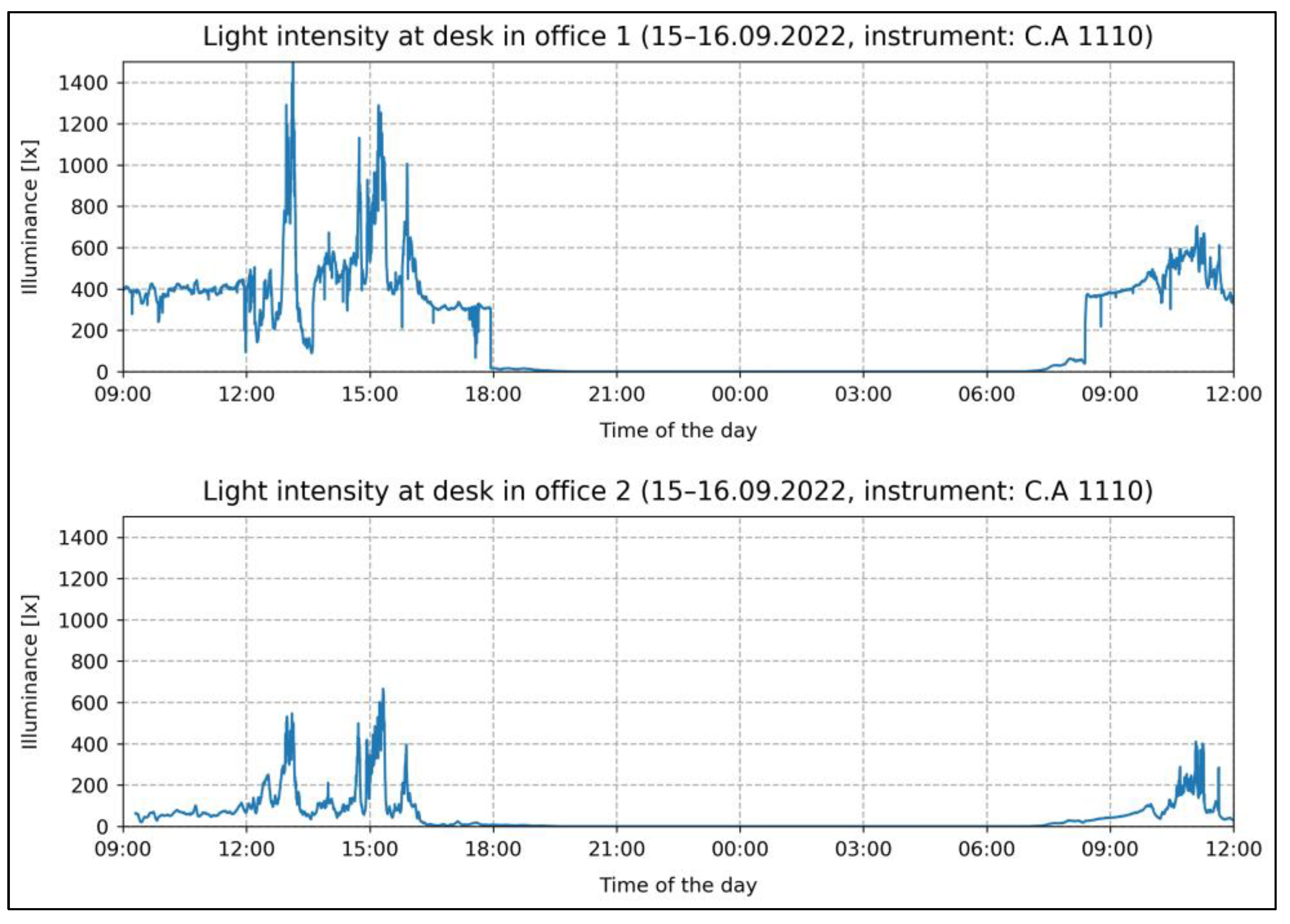
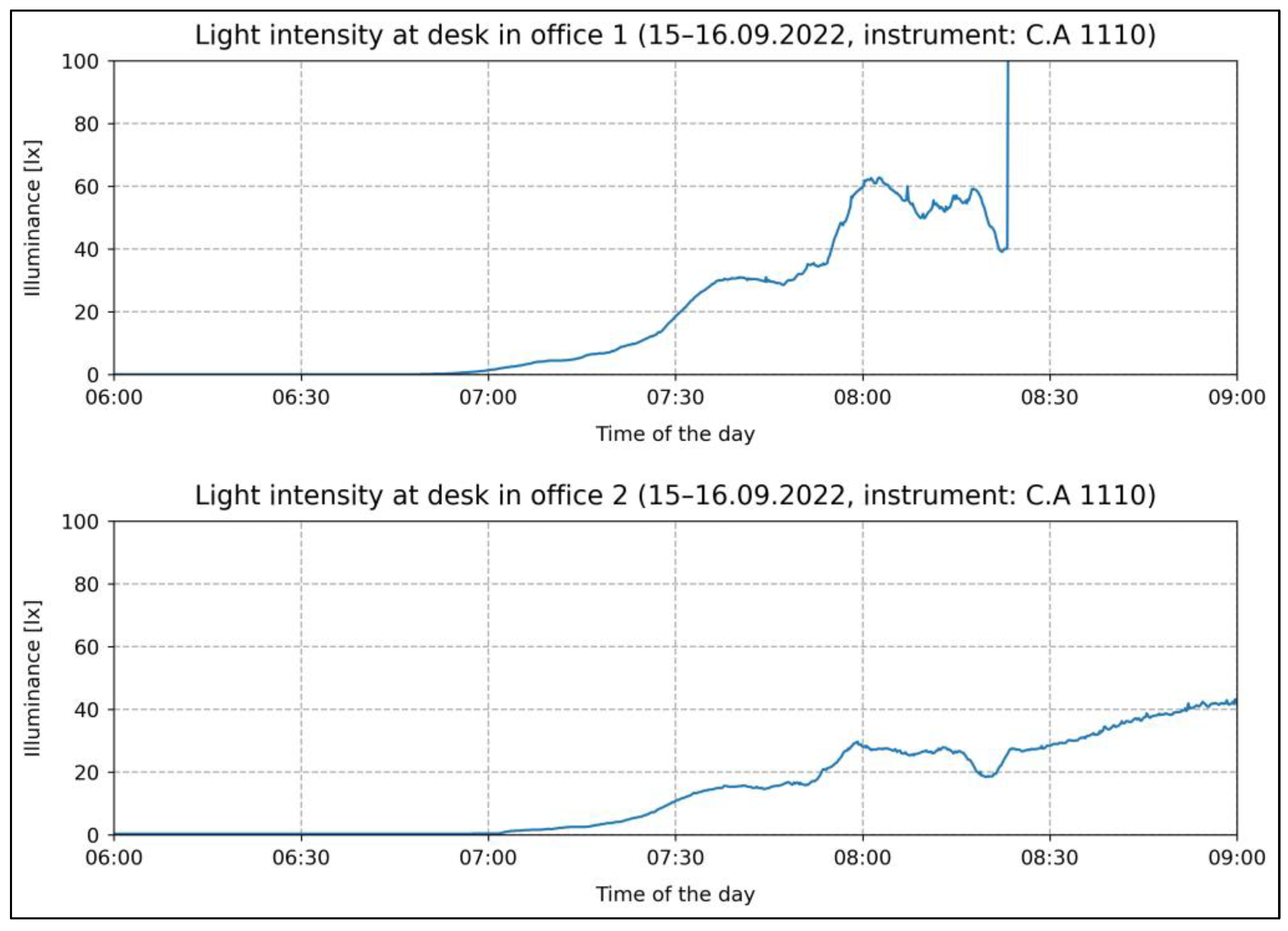
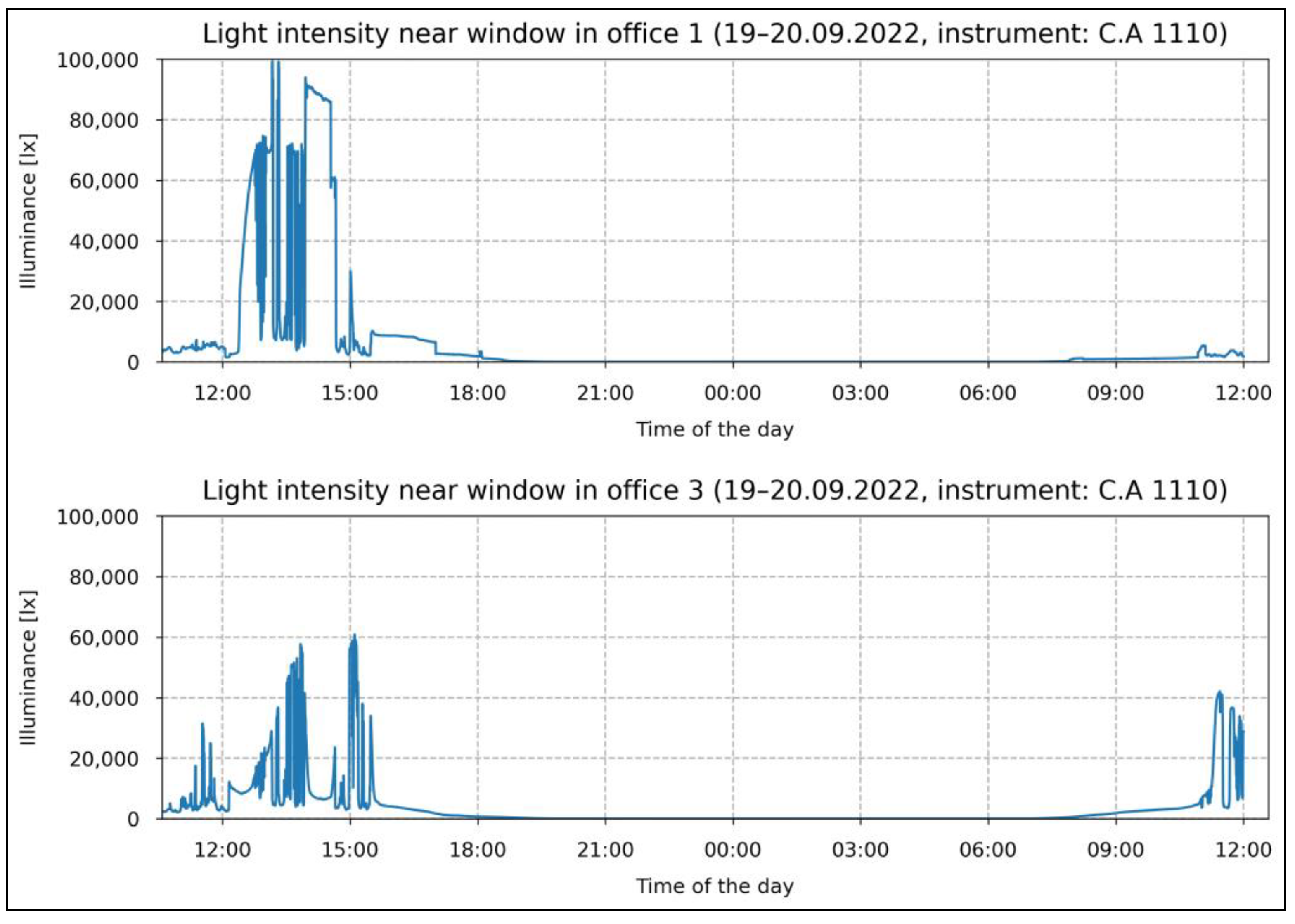
- Interior parking lots, stairways and corridors: 50–100 lux.
- Classrooms and studying places in general: 300–500 lux.
- Offices in general: 300–500 lux.
- Case 1: Places where there are periods of good illumination. Part of the harvested energy can be kept in a fitting energy storage method and used to power the system when light intensity levels are no longer sufficient. An appropriate storage management system is needed, which comes at extra cost, space, and sophistication. This is the method used in most systems. The authors of [12] provide one of the many examples that work in that way. The sophistication is partly related to characteristics such as the discharge current, the number of charge/discharge cycles, and the operational temperatures. The small number of charge/discharge cycles often contributes to shorten the lifetime of the product. However good the storage is, it will not do for spaces that are permanently under low light. This case is not the focus of this work.
- Case 2: Places that are poorly lit, either always or for so long that storing enough energy is not a viable solution. This might be the case for corridors or parking places in buildings. It is currently difficult to use solar harvesting in such places. Few works dealing with this case have been reported, as far as we know. The state-of-the-art analysis in Section 2 especially looks into works that have been found.
- Case 3: Situations where the illumination constantly varies. This happens, for instance, when dealing with portable systems powered by solar cells (such as those that can be worn). Space is very limited. The illumination on a wearable depends on how the device is worn, how it is orientated, and where it is. Solar-powered watches can be included in this category.
- Use appropriate harvesters. That means solar cells that can harvest sufficient energy at the light levels of the operating environment (compatible with light sources used indoors).
- Ensure low-power cold start. Reduce the amount of energy necessary to start up and keep the harvesting process going. If the energy accumulation process cannot start and be sustained, the system will not cold-start when the stored energy reserves have been used up. Consequently, losses in storage and power management must be kept low.
- Choose low power loads. Reduce the energy consumption of the various loads when the system is active, in order to save energy.
- An overview of the state of the art (SoA) related to important components and the SoA of comparable systems is given. The main contributions of this work are listed.
- The system that was designed and tested is described.
- The setup used for the evaluation is described.
- Results of the measurements related to the low-power performance are shown and discussed.
- Future works and a conclusion are given.
2. State of the Art Review and Main Contributions
2.1. Examples of Some Solar Cells on the Market (the List Is Not Exhaustive)
- The BCS4430B6 device from TDK has a surface with dimensions of 44 mm × 30 mm. Its datasheet gives an operating current of 30 µA for an operating voltage of 2.6 V at 200 lux [19]. Based on those values, the calculated electrical output per surface unit at 200 lux is ~6 µW/cm² (illuminated by white fluorescent light).
- Lightricity gives 22.1 µW/cm² at 200 lux (white LED light) for their EXL1-1V20 solar cell module [20]. The Lightricity solar cell technology is also used for the AMANDA project and for this work.
2.2. Solar Cells and Harvesting Architectures
2.3. Examples of IoT Systems Powered with Solar Cells (They Mostly Work at 100 Lux or Above)
2.4. Systems Working at 30 Lux or Below
2.5. Other Components Important in This Work (the List Is Not Exhaustive)
2.5.1. RTC and Low-Power Timers
- The PCF2131 of NXP is a temperature compensated RTC that can work from 1.2 V to 5.5 V (clock operating voltage) [42]. It typically consumes 64 nA at 3.3 V and can communicate with a host microcontroller using a serial link. The device does not have any extra memory for user data.
- The RX-8731LC of Epson [43] is a timekeeping module with an RTC and a built-in frequency-adjusted 32.768 kHz crystal. It can work between 1.5 V and 5.5 V and includes 80 bits of EEPROM for user data. The current consumption is typically 350 nA with a maximum of 800 nA at 3 V.
- The devices of the Artasie family of the manufacturer Ambiq (AM0805, AM0815, AM1805, and AM1815) [44] are RTCs that can run using their internal RC oscillator when accuracy constraints are more relaxed. They can also run with an external crystal to provide more accurate timekeeping. They work from 1.5 V to 3.6 V, and their energy requirements depends on the type of oscillator that is used. The lowest current requirement is achieved when the system runs uncalibrated with the RC oscillator (14 nA typical, 220 nA maximum at 3 V). In an intermediary mode, regular autocalibration of the RC oscillator is possible against the crystal oscillator that must therefore be activated. The AM1815 requires 22 nA typically and 235 nA maximum at 3 V. In the most accurate mode, it runs on a crystal. It consumes 55 nA typically, and at the most 330 nA at 3 V. The devices can communicate with a host MCU using a serial link. A 256-byte SRAM memory block is available for user data.
- The TPL5110 of Texas Instruments [45] is a nano timer that consumes 35 nA at 2.5 V (typical) and 50 nA max. It works between 1.8 V and 5.5 V. It can be used to time events. The time interval is set using an external resistance that is read at start-up. The extra energy required at cold start to read the external resistance should be considered, especially when there are frequent cold starts. The manufacturer has other variations of the product, with various features. The TPL5110 is not as accurate as devices that use a crystal.
2.5.2. Touch Detection
2.6. Main Contributions of This Work
- An autonomous short-range wireless sensor is designed, capable of cold-starting and working in poorly lit environments, down to 5 lux with a small solar cell module of 4 cm2. The node mainly uses commercially available components. This seriously improves on the current state of the art of 20–30 lux using components that can be found on the market.
- Based on the given components, the system is used in a low-power wake-up concept that keeps the high-energy consumers (microcontroller and radio) switched off most of the time. This reduces the load during the harvesting process while allowing sensing and accurate timekeeping to proceed. The MCU can be powered up periodically by an accurate real-time clock (RTC) or asynchronously by a user’s touch action. The current consumption of the combined active touch scanner and RTC is below 200 nA at room temperature, allowing them to be powered with very little energy from the harvester.
- The given low-power capacitive sensor can be used for touch detection (detecting the presence of a human body) or to measure parameters that can be related to capacitance values. That device may be configured via an OTP (one-time programmable) to control the energy supply of an embedded system. The sensor can be powered directly with the harvested energy.
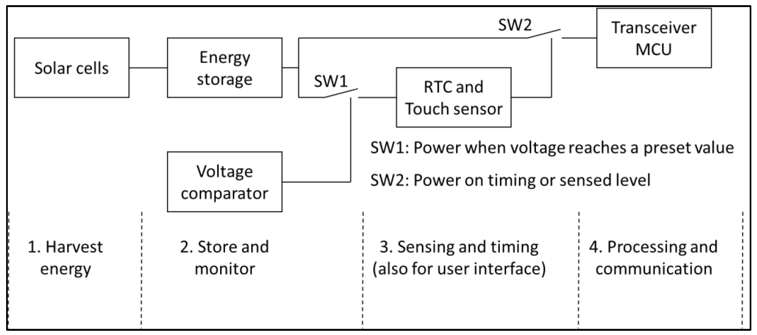
3. Description of the System
- (1)
- The energy harvester module, which in this case is composed of 4 small solar cells.
- (2)
- The energy store and its monitoring system. The harvested energy is accumulated in a 100 μF capacitor. The amount of energy stored is related to the voltage of the capacitor by E = 0.5 × C × V2, where E is the energy, V is the voltage developed across the capacitor, and C is the capacitance. The energy storage is monitored using a low-power comparator. Once the store’s voltage reaches a predetermined value, the electronic switch SW1 is activated to allow the stored energy to be used for the wake-up subsystem.
- (3)
- The RTC and the touch sensor. These are low-power elements used for timing activities (RTC) or as a sensor for applications where capacitive sensing is needed. In this work, they are used to detect a finger touch. The sensors are used to switch on a more demanding load at the convenient time, via switch SW2.
- (4)
- The MCU and transceiver. The MCU is used to process information and control the application. It is cold-started by a timing pulse from the RTC or by a touch event. The MCU can also communicate wirelessly with other nodes, enabling it to share information. The processing and communication power requirements should be within the available energy budget (that is, the energy delivered by the harvester or stored in the capacitor).
- In general, small solar cells deliver small amounts of energy. This is even more critical at low light intensities. One is here in the realm of hundreds of nanowatts to a few microwatts of input power. As examples:
- o
- The indoor solar cell manufacturer Epishine report in their datasheet an output of 14 μW for a 50 mm × 20 mm cell, at 50 lux. Assuming a linear relation between illuminance and output power, one reaches 1.4 μW @ 5 lux for a 10 cm2 cell [53]. That is 0.14 μW/cm2 at 5 lux. A 4 cm2 cell used at 5 lux within a system with 80% energy transfer efficiency will thus deliver 448 nW of power (0.14 μW × 4 × 0.8).
- o
- The solar cell manufacturer Lightricity reports 22.1 μW/cm2 at 200 lux for their EXL1 solar cell [19]. Assuming a linear relation between illuminance and power and 80% transfer efficiency, this corresponds to 1768 nW of power for a 4 cm2 cell at 5 lux (22.1 μW × 0.8 × 4 × 5/200).
- The small amount of available energy means that care should be taken to reduce leakages during the harvesting process, to be able to cold-start and reach a voltage level that is necessary for the electronic components to function. To achieve that, the harvesting process is isolated using a switch controlled by the low-power comparator. The current consumption of the comparator and the leakage of the storage have a negative influence on the harvesting process. These elements should therefore be chosen appropriately.
- MPPT is a process that enables the optimal transfer of energy from the solar cell. That process itself requires energy. MPPT is not used here because only a very small amount of energy is expected at low illumination.
- In general, the voltage delivered by the solar cell decreases as the illuminance is reduced. In order to reach the required voltage level, a booster can be used, which often requires additional energy to start up. For example, the EM8500 power management device typically requires 3 μW for a cold start and 1 μW while running [54]. The AEM10941 power management device requires a minimum of 3 μW to cold-start [55]. In this work, the alternative chosen to avoid the relatively high energy requirement of boosters at start-up is to connect several solar cells in series, which leads to additional components.
- The wireless system chosen is BLE. Data can be transmitted in ADV or in connected mode using a certified BLE system-on-chip (SoC). This wireless system requires tens of microjoules per frame while transmitting at 0 dBm [56].
Main Components
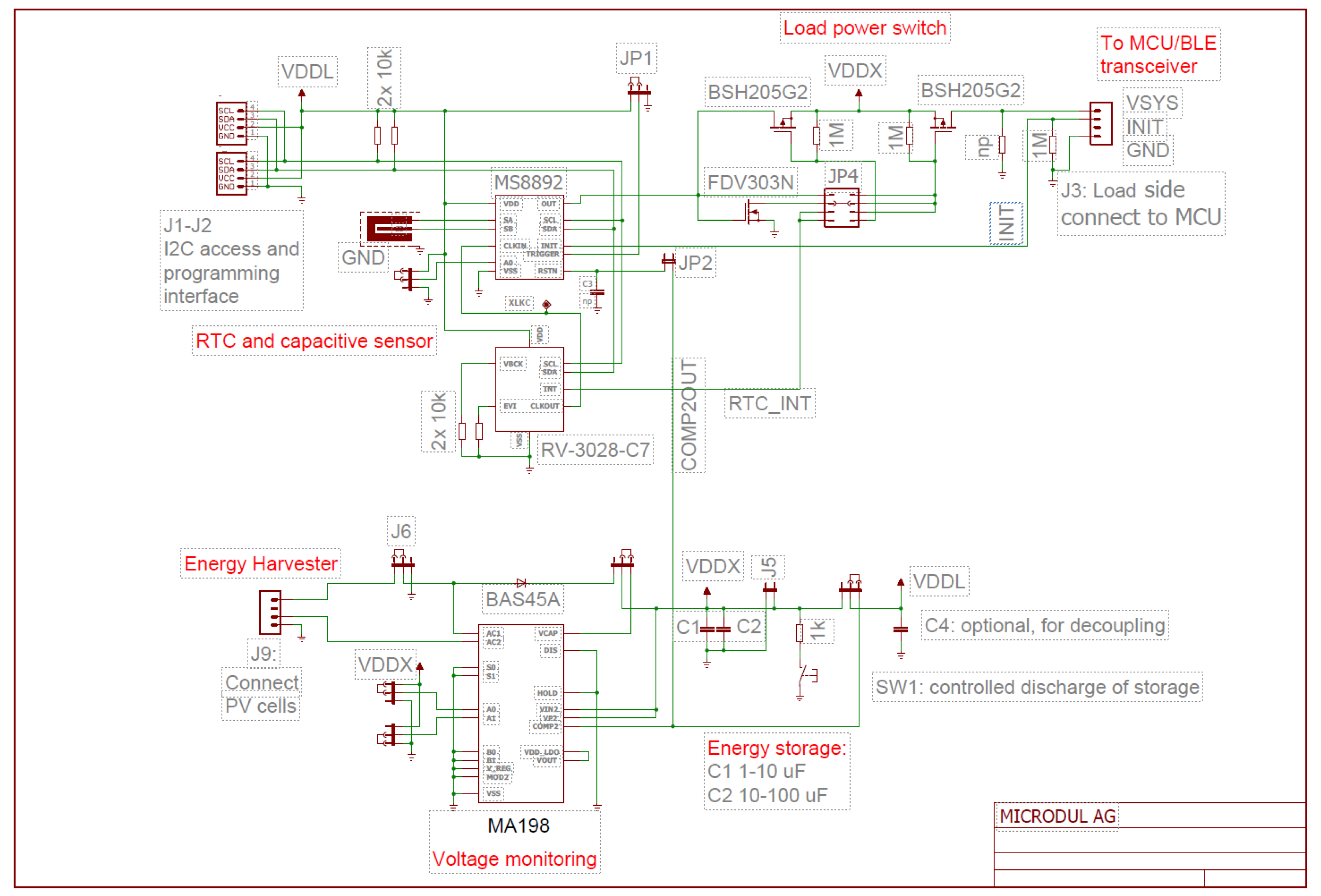
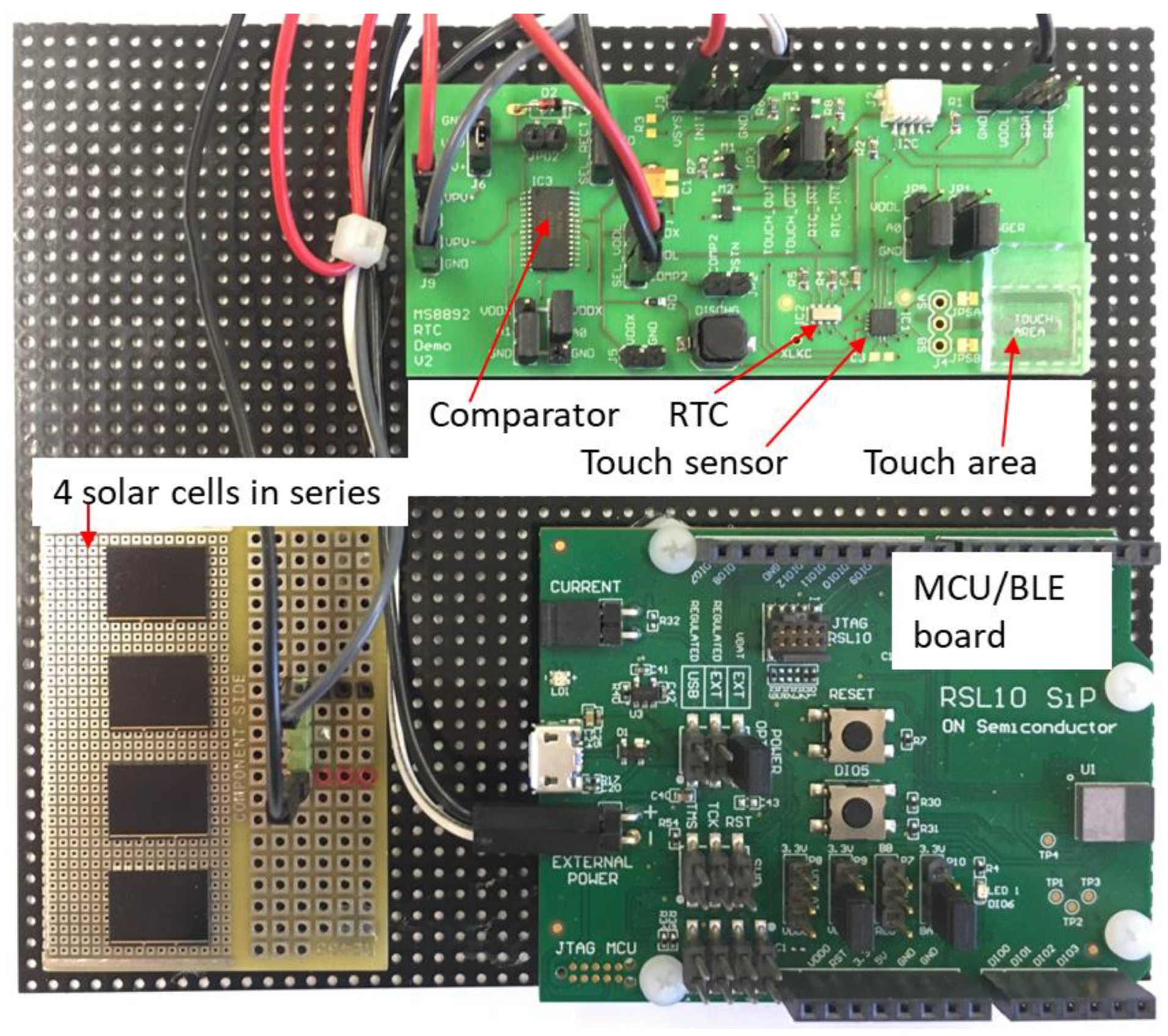
- The module consists of four EXL1-1V20 cells from Lightricity. Each cell has a surface of 98 mm2 (approximated in this work to 1 cm2). The technology enables high indoor and outdoor efficiencies. High-purity III-V material is used for the cells. The lifetime is quoted as above 20 years. According to the manufacturer, no extra diode is needed between the cell and the storage. The energy output at 200 lux is given as 22.1 μw/cm2 (white LED spectrum), for an operating voltage of 1 V and an current of 21.7 μA. According to the manufacturer, “Lightricity PV technology achieves a conversion efficiency over 35% in the lab, and over 30% in production” [58].
- The MA198 power manager [59].This is a device from Microdul AG and Algra AG in Switzerland. It was designed for energy harvesting and other low-power applications. It allows a storage element to be charged by an external harvester source, with minimal interference with the final load. In this work, only a single comparator of the MA198 is used. The comparator monitors the voltage of the storage capacitor and separates the solar cells and storage from the load during the initial energy harvesting process. Once a predefined voltage is reached, energy is allowed to flow into the load. A built-in hysteresis avoids unwanted restart operations. The device typically requires 30 nA at room temperature. In this work, the threshold for detection was set to 2.4 V using external pins (2.25 V measured). The use of the comparator enables the system to harvest and accumulate, even when the power delivered by the solar cell is very small (low light intensities).
- This low-power RTC module is manufactured by Micro Crystal. It integrates a real-time clock and a 32 kHz crystal quartz, conferring it an accuracy of ±1 ppm at 25 °C. An integrated EEPROM allows parameters to be configured and re-read, even after a power failure. The device works between 1.2 V and 5.5 V, typically requiring 45 nA at 3 V (60 nA maximum at 3 V). More when driving an external load. The module can work in stand-alone mode, using parameters read from its EEPROM when it powers up. It can also communicate with a host using its I2C bus. It can be programmed to generate interrupts or to control other circuits. In this work, the RV-3028-C7 is foreseen as a low-power accurate timer, capable of starting the embedded system at defined time intervals. It also generates a synchronous signal that pilots the capacitive touch sensor. That leads to a lower current consumption than if the touch sensor is clocked internally. Low power consumption in active mode is important. The energy requirements at cold start are also fundamental, as they affect the amount of energy that should be accumulated before a cold start is possible.
- The MS8892 capacitive touch sensor [63].This device is an ultra-low-power capacitive sensor and touch switch for human body detection and system wake-up. The device incorporates a memory latch to keep the power state active until the system controller decides to shut down the active power once the processing and communication tasks are completed. The flexible and fully configurable output logic of the MS8892 also allows setting the power-state latch by external wake-up sources (like the RTC in the present architecture, or other wake-up sources). A selectable absolute or relative capacitive switching threshold allows for compensation for material and fabrication variations of the sensor electrodes. With an active power consumption of 720 nA in stand-alone operation and 65 nA when clocked externally, the MS8892 is optimally suited as an ultra-low-power system power controller and many other applications where energy is a limited resource. At 3 V, that is 195 nW (external clock energy not counted).In the AMANDA project, the MS8892 is used to enable asynchronous user interaction. By touching the sensor electrodes, the user can trigger a wake-up from the lowest-power mode. The device then routes power to the MCU system, allowing it to cold-start. After powering up, the capacitive touch sensor remains active and is used for user interaction with the system. The ability to configure many parameters of the RTC and the capacitive sensor in non-volatile memories (respectively EEPROM and OTP) enables the selection at cold start of certain system functions, without the need to first start and use the microcontroller. This in turn adds an important flexibility and low-power dimension at start up.
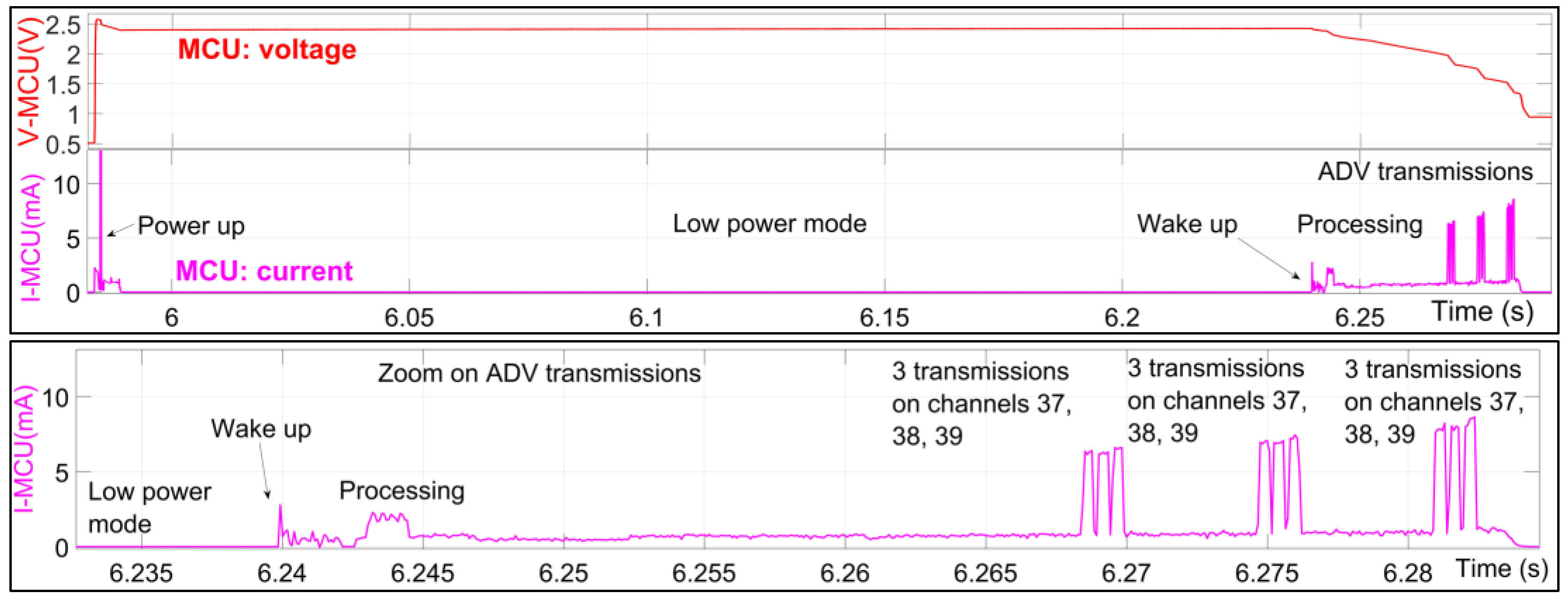
- The RSL10 is an SoC that integrates a Cortex-M3 microcontroller and a BLE transceiver. The device is Bluetooth® 5.2-certified and supports various proprietary transceiver modes. It also has DSP functionality and support for 802.15.4 wireless protocols. It is used as a BLE controller in the AMANDA project. Bruetsch et al., measured the energy performance of several BLE transceivers in different communication modes [56]. Their work details the energy requirements in different communication modes. The paper demonstrated that the RSL10 has a good energy performance, requiring just tens of microwatts to transmit full ADV frames (advertisement mode). According to the authors, it is possible after optimisation to cold-start the RSL10 and transmit one ADV packet of 47 bytes per frame with less than 30 μJ. The device is also sold in a system-in-package (SiP) fashion, where the SoC and some of the required components, such as crystals, antenna, capacitors, and others are in a single space-saving package. This work uses the RSL10-SIP-001GEVB development board integrating the RSL10 SIP. The load is powered using the harvested energy. The MCU is programmed to behave as described below:
- o
- Upon power-up, a minimal check is made, and some registers are initialised.
- o
- The MCU then goes into deep sleep mode for about 250 ms, where its current consumption is reduced.
- o
- After the deep sleep, the device initialises its BLE radio and starts ADV_NONCONN_IND advertising events.
- o
- Packets are advertised on channels 38, 39, and 40, with the RF output power programmed for 0 dBm. The transmitted frames have a length of 39 bytes, or 47 bytes in total when the overhead and preamble are counted. Figure 7 shows the corresponding energy trace, captured while powering the programmed RSL10 with the measurement tool.

- External clock source, 1024 Hz.
- Periodic sensing, 8×/s. Output polarity setting.
- Relative threshold mode with the threshold set to 0 × 0 A.
4. Setup
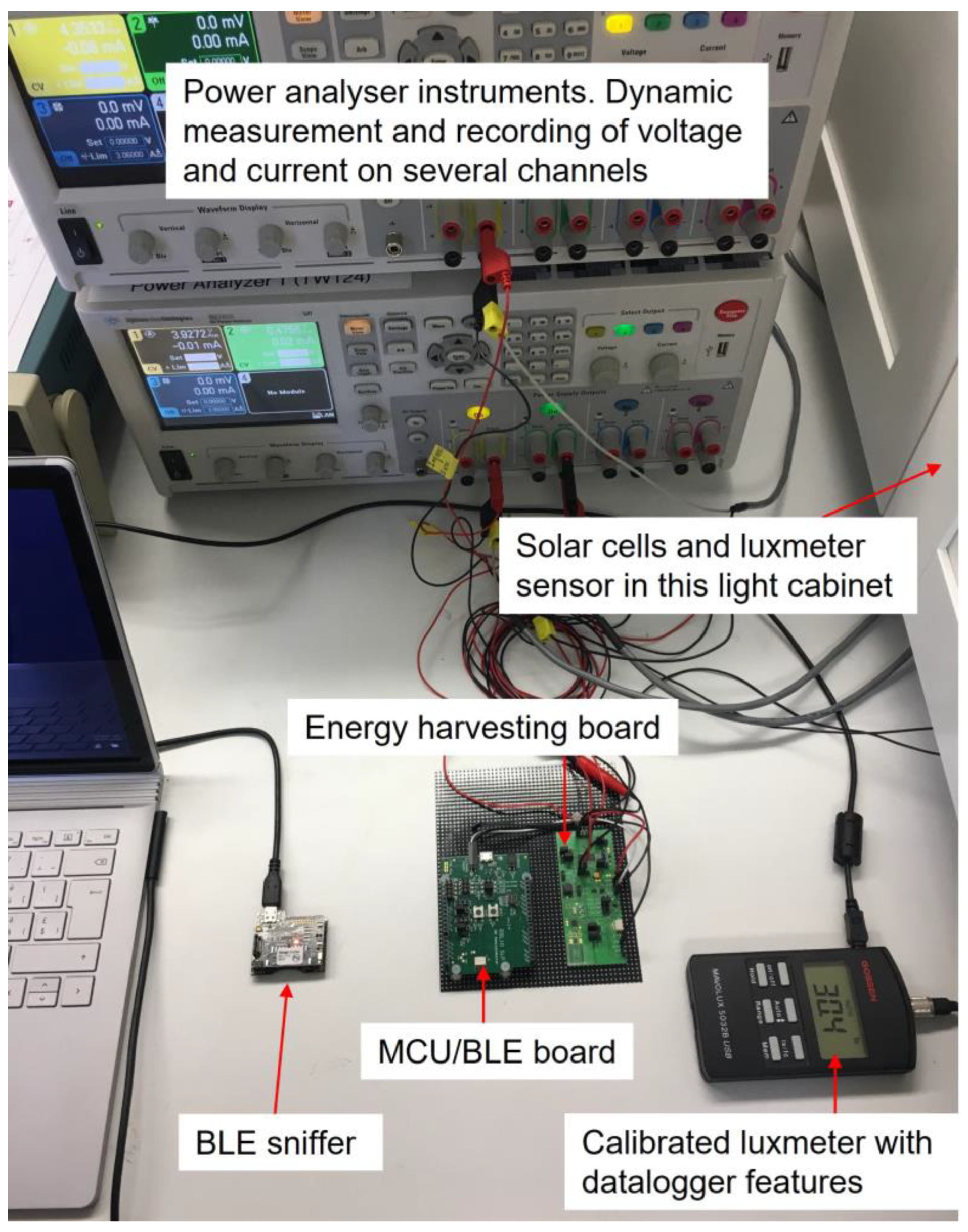
- The power analyser: N678xA from Keysight [67].Up to two instruments were used in order to have enough channels to measure and log various parameters simultaneously. Voltages and currents at different stages of the architecture were measured, and the power and energy were calculated directly by the instrument. Most measurements reported here were made with the power analyser.
- The luxmeter: a calibrated Mavolux 5032B USB [68].This instrument was used to monitor and to log the illuminance.
- The BLE sniffer from Texas Instruments [69].It was used to capture BLE frames (ADV frames for this work). Only one channel was sniffed at the time. The results shown in this paper for ADV channels therefore only relate to one ADV channel, although frames were sequentially transmitted on all three channels.
- The connected boards with the following elements:
- o
- The solar cell module.
- o
- The energy harvesting board with the comparator, RTC, and touch sensor.
- o
- The MCU development board with the RSL10 SiP device.
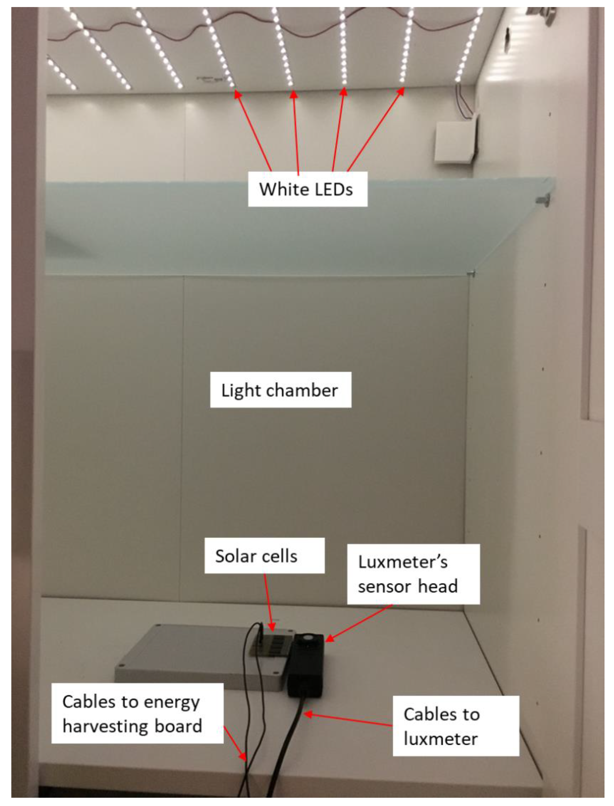
- The light cabinet.For the tests, the solar cells and the luxmeter’s sensor were kept in a chamber illuminated using white LEDs, as shown in Figure 10. The intensity of the LEDs was controlled using an appropriate external power supply. A luxmeter was used to set the desired light intensity and to log its value during the tests. There is a glass between the LEDs and the device under testing and luxmeters, which helps in setting small intensities but also has an impact on the light characteristics. The walls are reflective, which is fitting for many indoor operating environments.
5. Results
5.1. Measurements on the Solar Cell Module
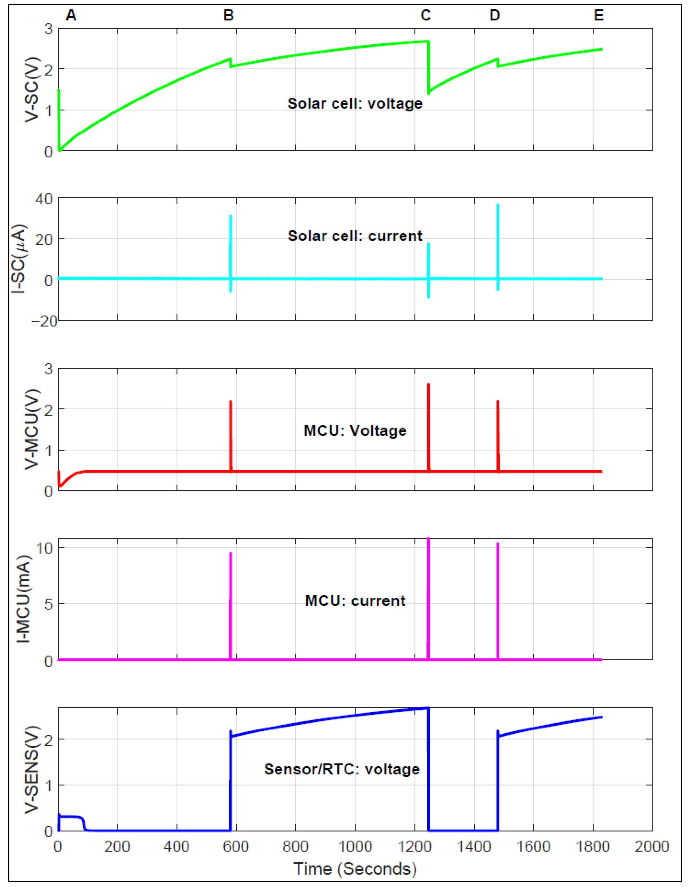
5.2. Results at 5 Lux
- Measure the current from the solar cell (I-SC) and its voltage (V-SC or VDDX).
- Measure the voltage of the sensor and RTC (V-SENS or VDDL).
- Measure the load current (I-MCU) and the voltage of the MCU (V-MCU or VSYS).
- I-SC and V-SC are the current from the solar cell and the voltage of the same, respectively.
- The storage capacitor has a self-discharge represented here by I-SDIS. It is charged with the current I-STOR. Its leakage is represented by I-SLEAK.
- The comparator needs power to monitor the storage capacitor. This is represented by I-CMP. When the comparator threshold voltage is reached, it enables the supply of voltage to the touch sensor and the RTC V-SENS. The devices consume a current I-SENS.
- The touch sensor and the RTC are used to control the power supply of the MCU load. The control elements are biased with I-CTR.
- The current in the MCU load is represented by I-MCU.
- At 2 V, the comparator typically requires I-CMP = 30 nA.
- The self-discharge of the storage capacitor measured at 2 V is approximately 15 nA
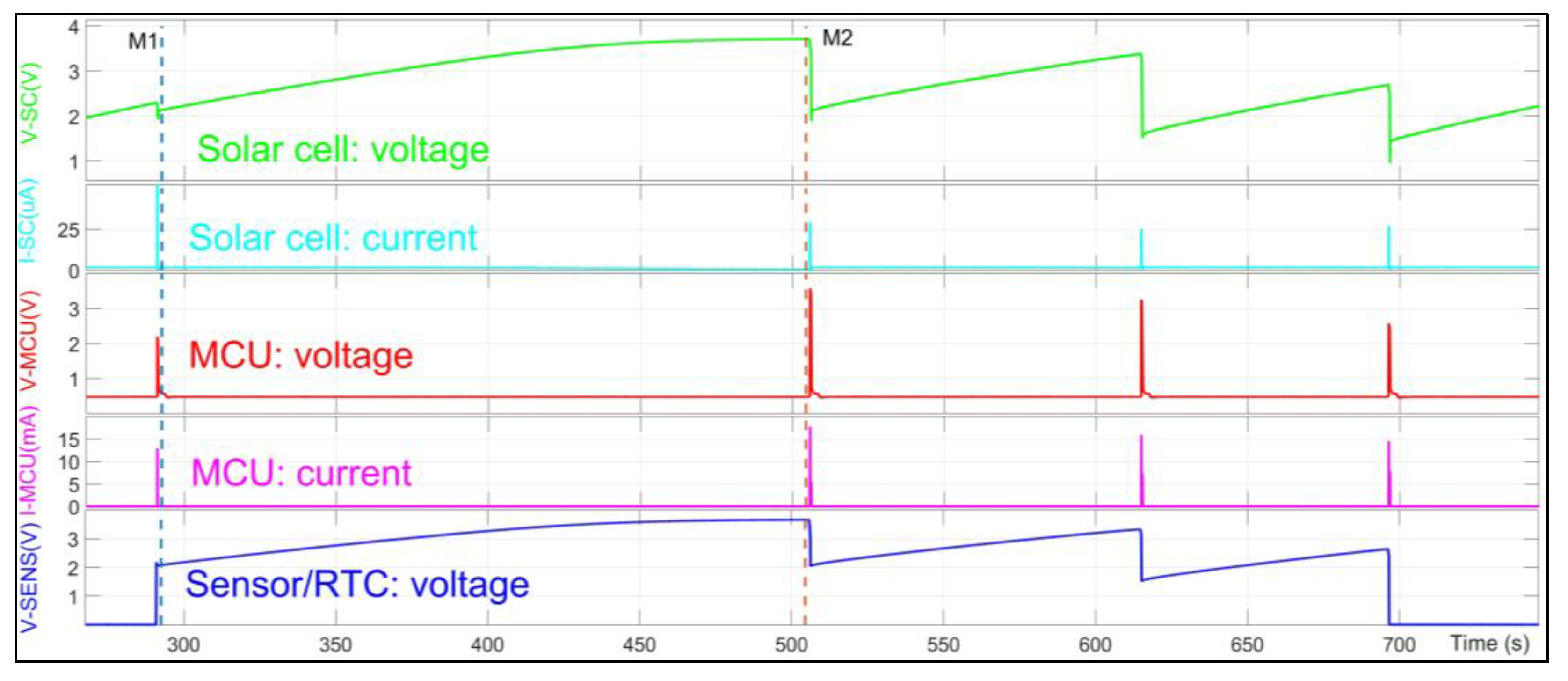
- Event A: The energy storage is discharged.The storage is manually emptied before the evaluation of the harvesting process begins. As the solar cell delivers energy, the storage voltage goes up. The comparator powers up with it and starts monitoring the storage’s voltage. As long as the voltage is below 2.25 V, the load on the solar cell only consists of the storage capacitor, the monitoring comparator, and small leakages. The RTC, sensor, and MCU are all switched off. The voltage of the storage element continues to climb.
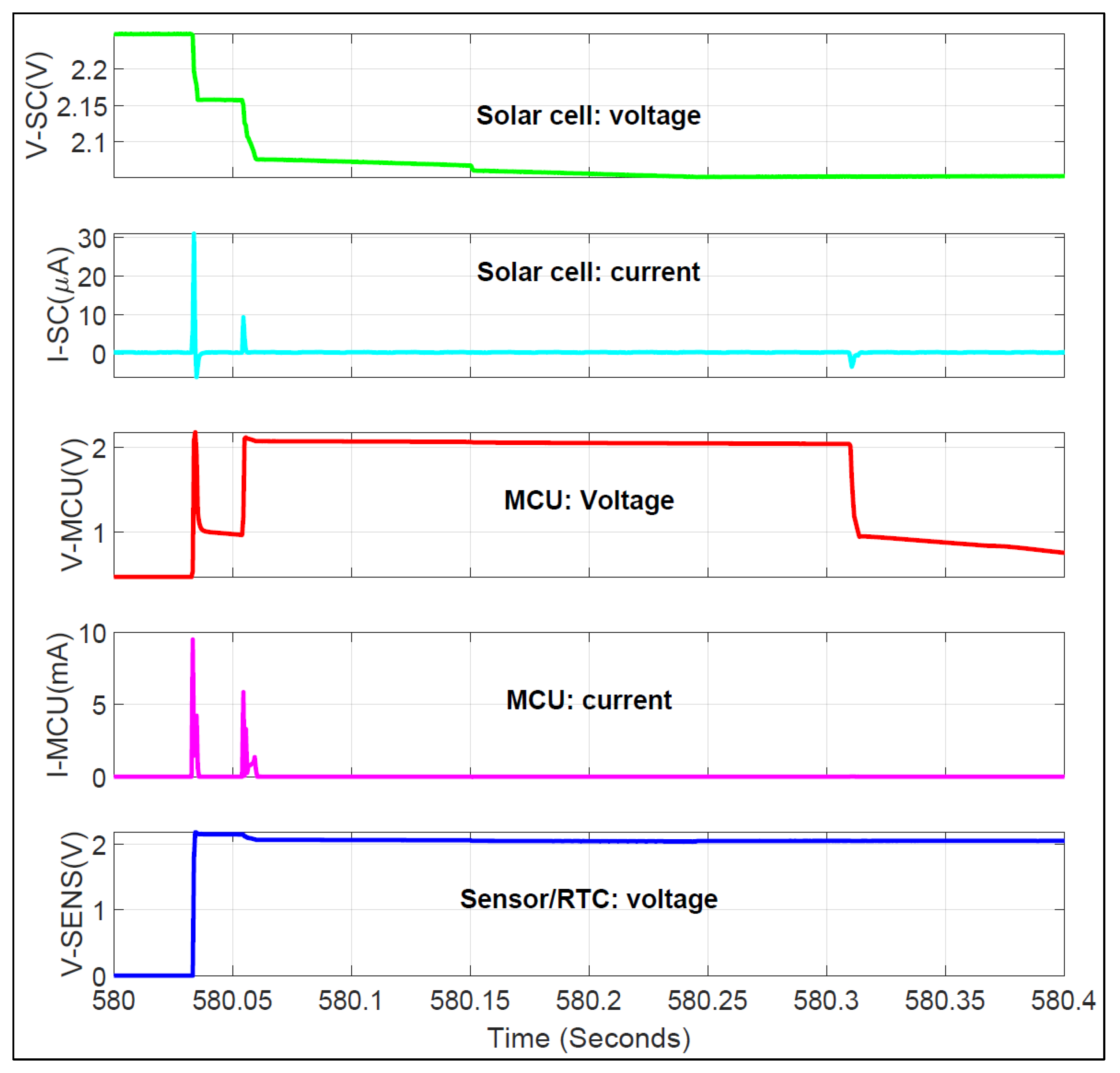
- Event B: The touch sensor and RTC are powered on.The threshold of the comparator is reached. The RTC and touch sensor are powered on, leading to a small voltage drop at B. After initialising, they are ready and active. The RTC generates the required clock signal for the touch sensor so that it can regularly compare the capacitance on its electrode inputs to the threshold and detect whether a touch action has occurred. The harvesting process continues, with the RTC and the touch sensor active. The voltage of the storage increases further.
- Event C: Touch detection and activation of the wireless MCU. System switches off.The touch activity is detected when a finger is placed on the electrodes. The sensor node routes power to the RSL10. The MCU starts up and transmits several frames. That process requires significant amounts of energy. The storage delivers that energy in a short time, and its voltage drops. The MCU activity continues until the storage voltage drops below the comparator threshold. The comparator cuts off the supply of both the timer and the touch sensor and thus of the MCU. The harvesting process continues from point C, and the voltage at the storage goes up again.
- Event D: The touch sensor and RTC are powered on.The voltage of the energy storage element has now reached the threshold set in the comparator, as in situation B. The sensor and the RTC are powered up and restart. The sensor is active and monitors the capacitance at its input pins. Harvesting continues, and the voltage of the storage element goes up.
- Event E: End of sequence.As long as there is enough energy from the solar cell, the voltage goes up until it settles, and the capacitive sensor continues measuring the capacitance at the electrodes.
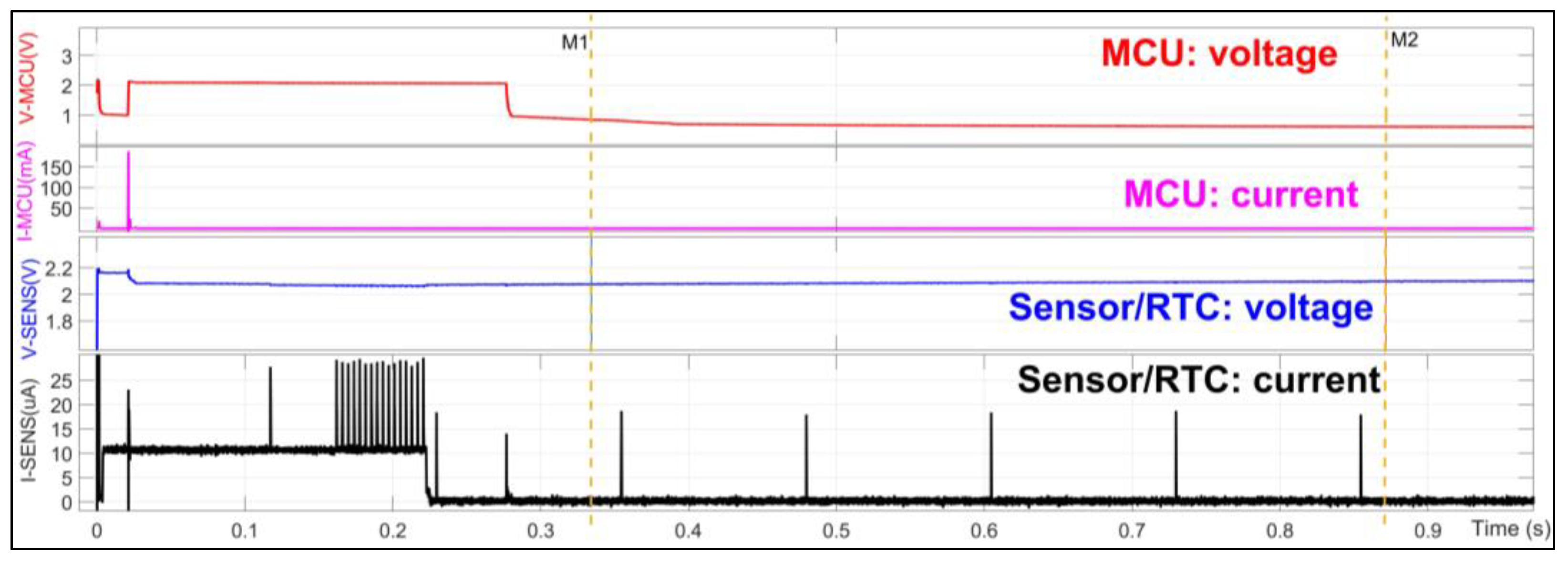
- A > to < B: Measurements shortly after A (M1) and shortly before B (M2) (Table 2).The average power delivered by the solar cell in this time slot is P-SC = 566 nW, with peaks of 1.14 µW. The total energy added during this time (T = 577.688 s) to the storage can be calculated as: 0.5 × 100 µF × ((2.25 V)2 − (1.03 mV)2) = 253 µJ. In the same time slot, 326.33 µJ is harvested. It means that an amount of 73.33 µJ is harvested but not added to the storage. It is lost in various leakages (the energy capacitor, the comparator, and the transistors in the control stage that deliver power to the MCU). The system requires less than 10 min at 5 lux to cold-start and be ready for operation.
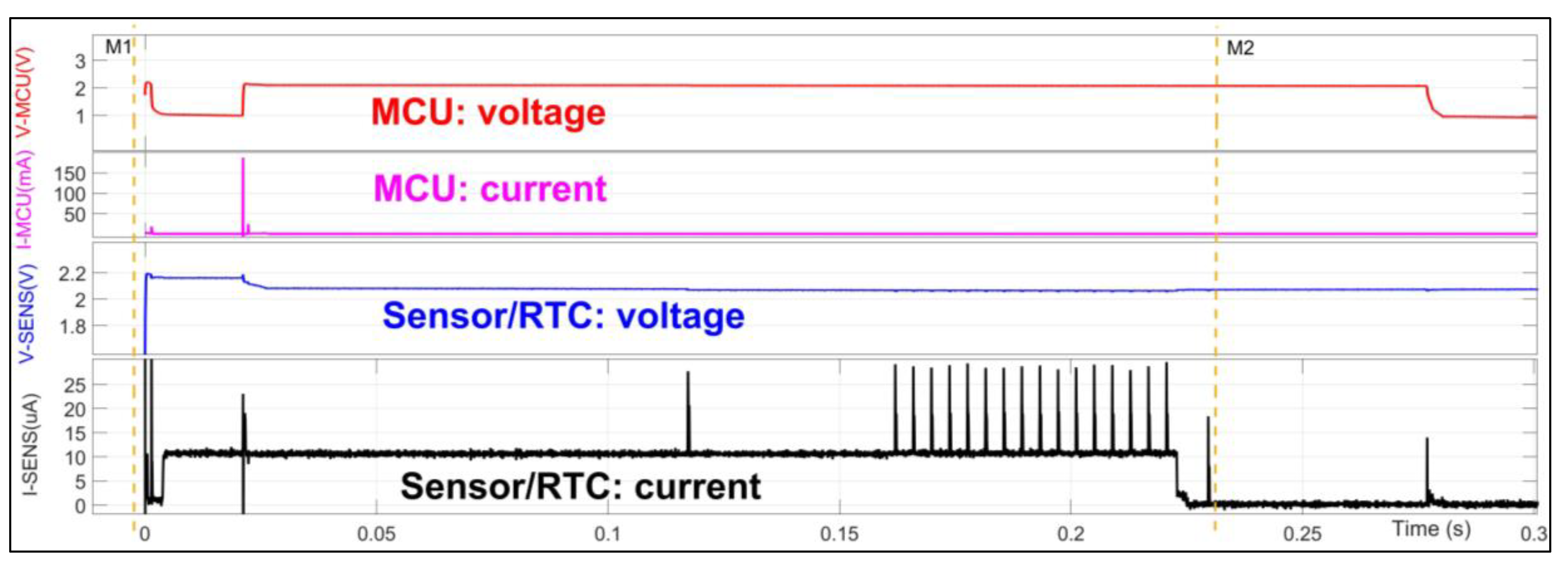
- Signals at event B:Figure 13 shows a magnification of the signals around the position of event B. During its start-up phase, the touch sensor shortly powers the MCU, which starts up and consumes some energy (30 µJ in 280 ms). This is seen on the signals V-MCU and I-MCU. Thanks to the programmed firmware delay, the MCU goes into a power-saving mode and does not process or transmit any frame. After booting, the MCU power is removed, and the sensor and RTC are active. The touch sensor then regularly measures the capacitance at the electrodes to check for a finger presence.
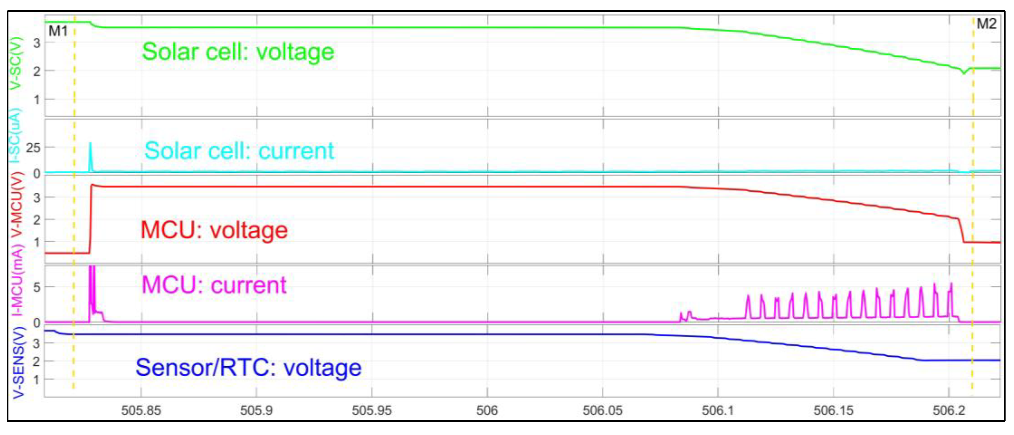
- B> to <C: Measurements shortly after B (M1) and shortly before C (M2) (Table 3).The average power delivered by the solar cell in this time slot is 856 nW, with peaks of 1.26 µW. In this phase, the energy is consumed by leakage in the storage, leakage in the power stage, the comparator, the RTC, and touch, as the RTC and touch are also active in this time window.
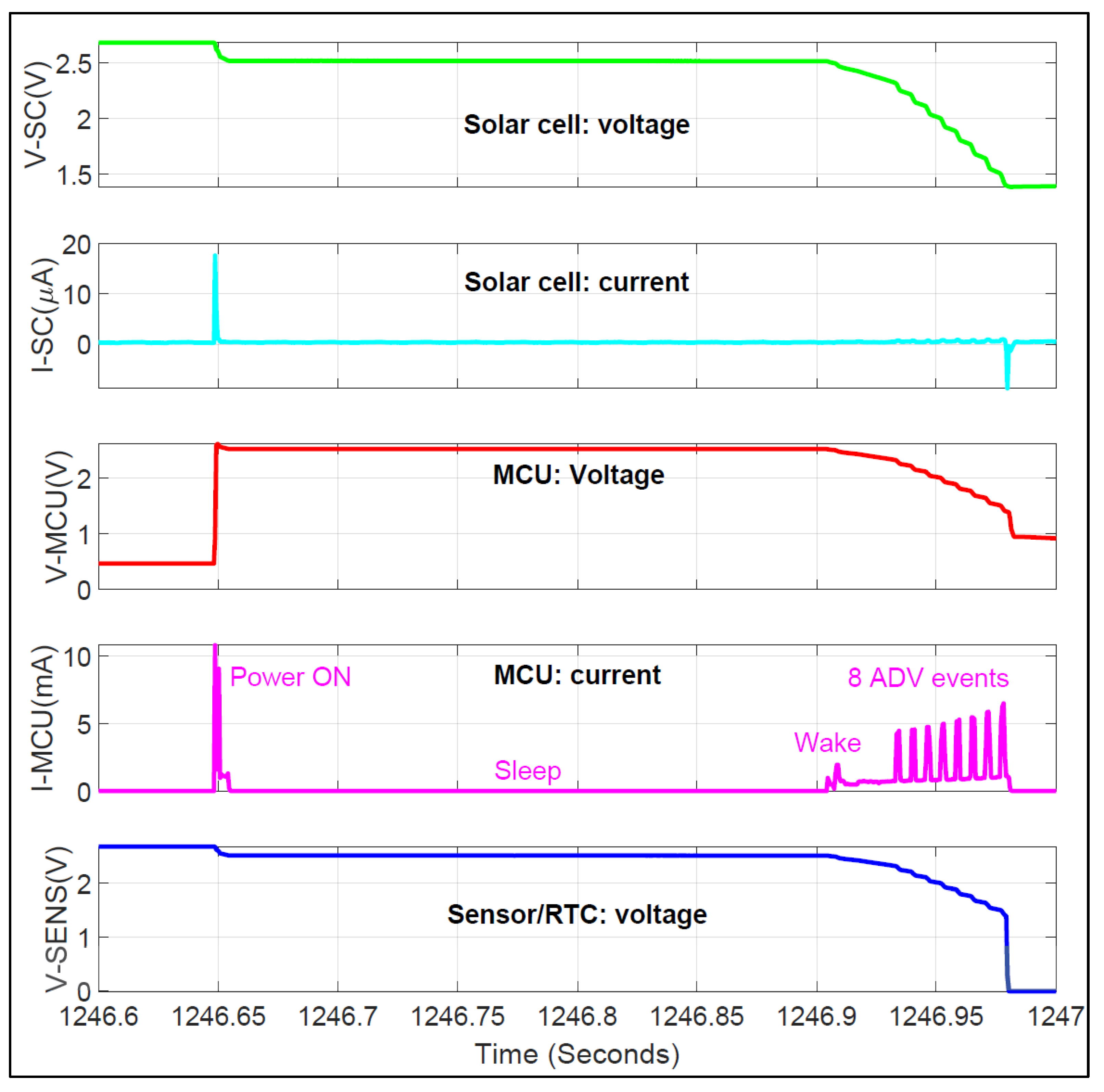
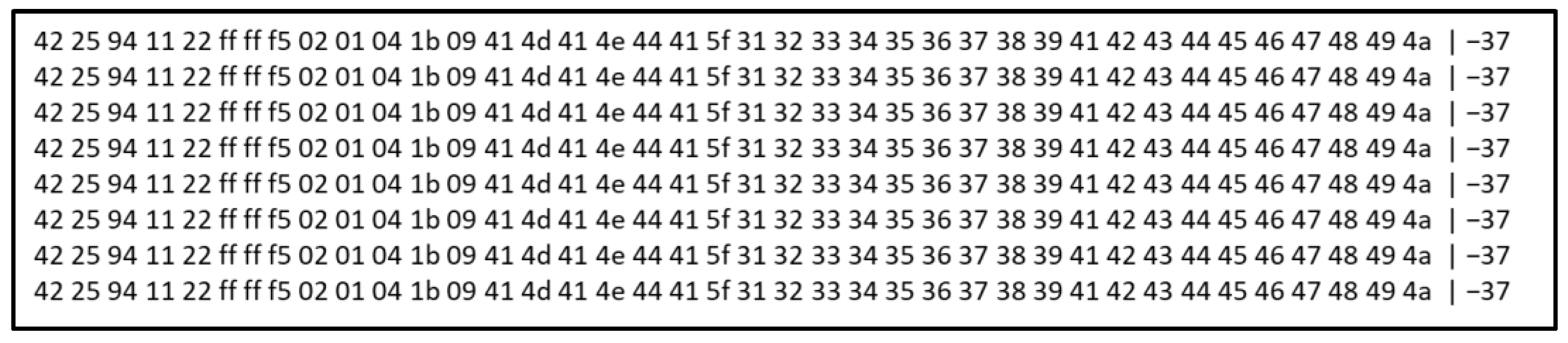
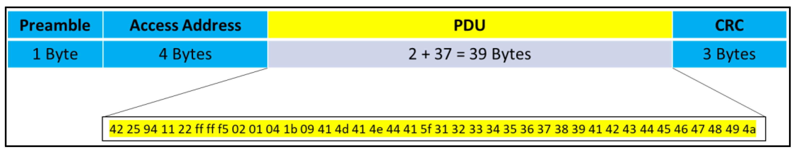
- Signals at event C:Figure 14 shows a magnification of the signals at position C. The MCU is powered on (time 1246.65 s). Initially, much current is drawn, which corresponds to the cold start of the MCU. After the sleep delay implemented in the firmware, the MCU wakes up (time 1246.9 s), goes into processing mode, and transmits ADV frames. Frames are sent until the MCU is turned off. The activities of the MCU last 335 ms and require a total of 262 µJ. They are divided into 34 µJ from power on until wake up from sleep, 48 µJ until the start of first frame, and 180 µJ for transmitting all the ADV events.Data transmitted during the ADV events are received by the sniffer (Figure 15). The same information is sent on the three ADV channels for each event. Because the sniffer only scans one ADV channel, 8 frames in total are received. The events correspond to the current peaks seen on the I-MCU current trace (Figure 14). The RSSI (received signal strength indicator) calculated by the sniffer has a value of −37 dBm for all frames (the sniffer acting as receiver is not far away from the transmitting device, as can be seen on the setup (Figure 9)).Figure 16 shows the structure of an ADV frame that is sent. The PDU (protocol data unit) has 39 bytes, corresponding to an on-air frame size of 47 bytes at 1 Mbps. In the best case, all 3 ADV frames of each event are transmitted, which means 8 × 3 = 24 frames. In the worst case, the last 2 frames of the last event (channel 38 and channel 39) are not transmitted. That means 22 frames are transmitted. Therefore, the energy harvested is enough to transmit at least 22 frames with a total of 47 bytes each.
- C> to <D: Measurements shortly after C (M1) and shortly before D (M2) (Table 4).The average power delivered by the solar cell is 765 nW in this time slot, with a peak of 1.13 µW. Here, the voltage has gone below the comparator’s threshold, meaning that the RTC and the touch sensor are no longer powered. However, the storage capacitor is already at 1.44 V. Current consumption is due to leakage in the storage, power stage, and supply current of the comparator. The RTC and the touch sensor are not active. The storage is being charged.
- Signals at event D:At event D, the comparator threshold is reached, and the touch sensor and RTC are powered. The system behaves as in case of event B. The energy storage was not fully discharged at event C. Therefore, event D is reached faster (here, 231 s). It means that the system reacts faster once it has been started. The application firmware can be written so as to switch off the MCU earlier and avoid that the RTC and touch sensor be switched off. That would allow the system to react even faster. In the case that the RTC is used for timekeeping, time information would not be lost. The RTC itself can accept a backup storage element that allows it to keep information for a certain time, even when power is not available. That feature was not used in this work.
- D> to <E: Measurements shortly after D (M1) and shortly before E (M2) (Table 5).The average power delivered by the solar cell is 841 nW in this time slot, with a peak of 1.21 µW. The power consumption is due to leakages and supply currents of the comparator, RTC, and touch sensor because those elements are active. The voltage of the storage capacitor goes up.
5.3. Results at 20 Lux
5.4. Energy Requirements of Touch and RTC
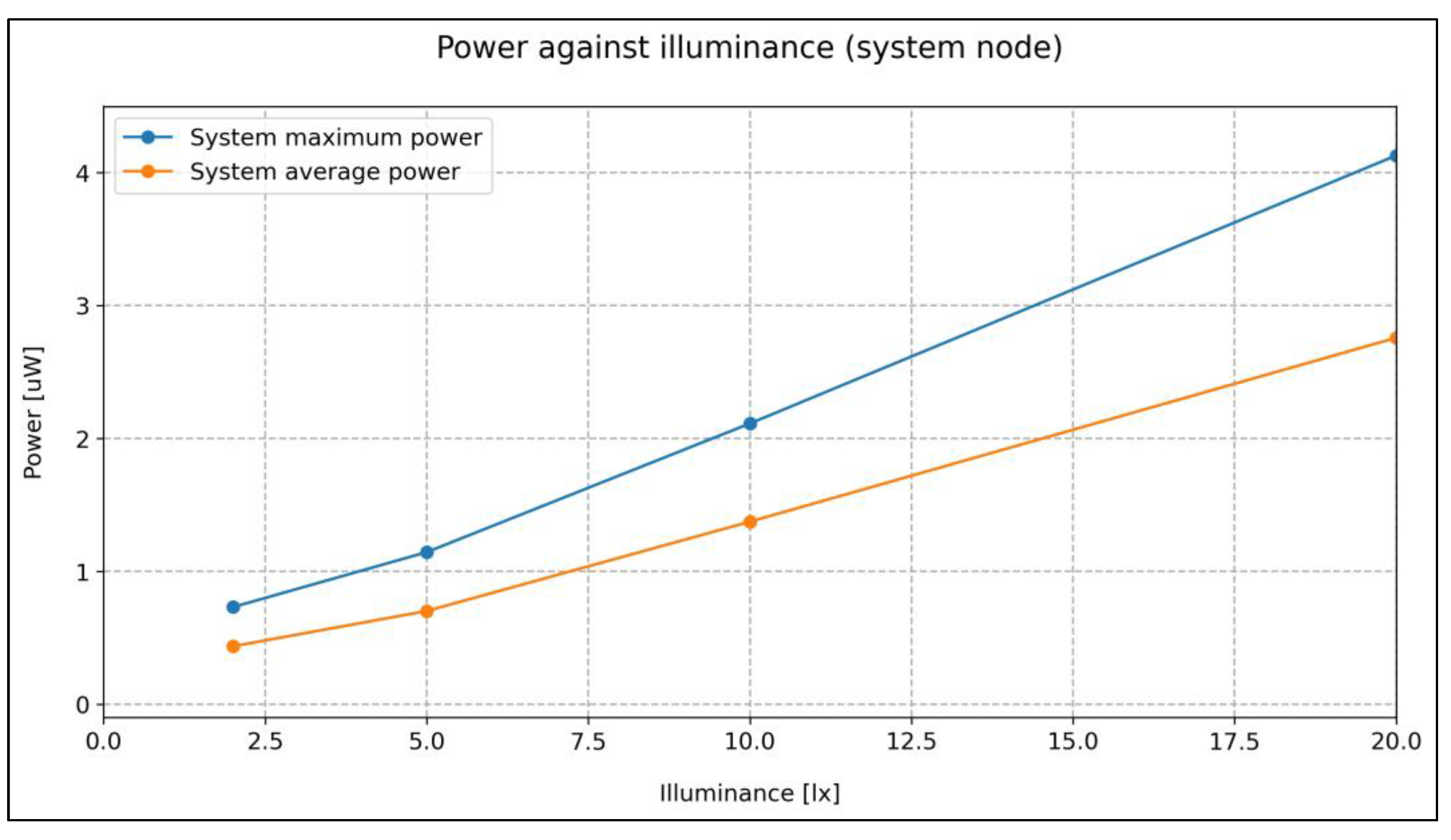
5.5. Harvested Energy at Different Illuminances
5.6. Limitations
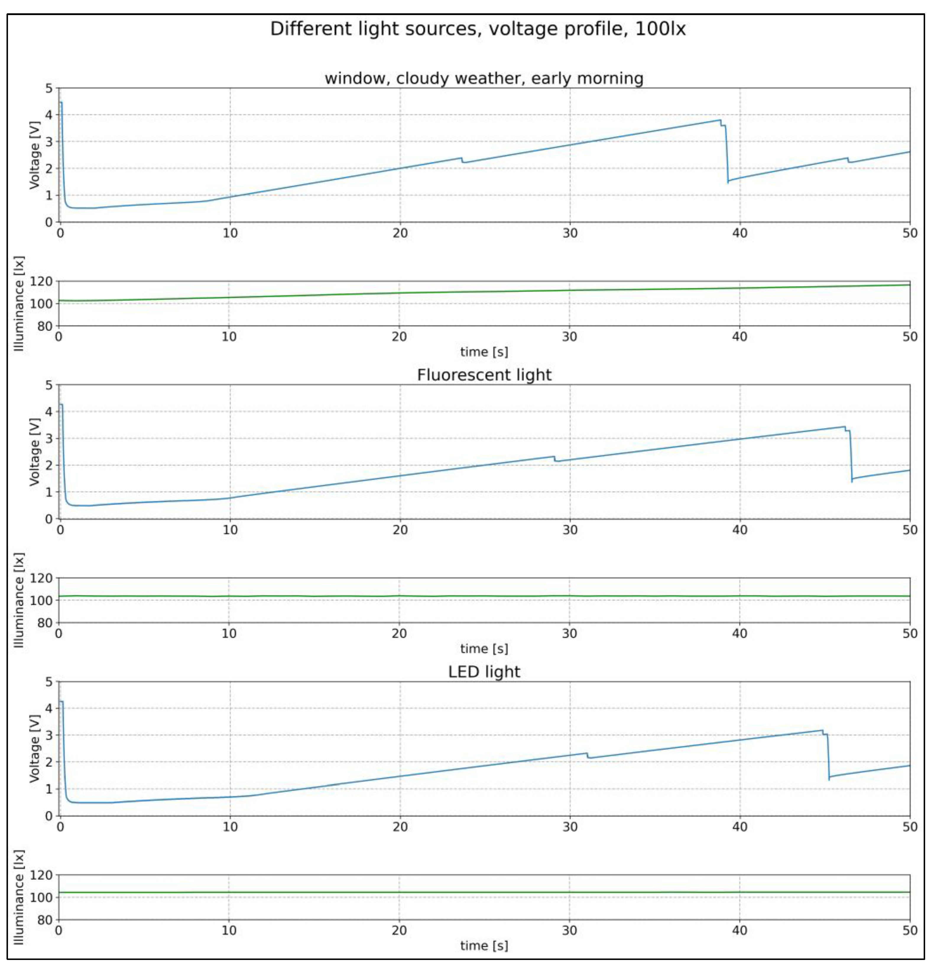
5.7. Measurements Using Other Light Sources
6. Conclusions and Future Works
Author Contributions
Funding
Institutional Review Board Statement
Informed Consent Statement
Data Availability Statement
Conflicts of Interest
Appendix A
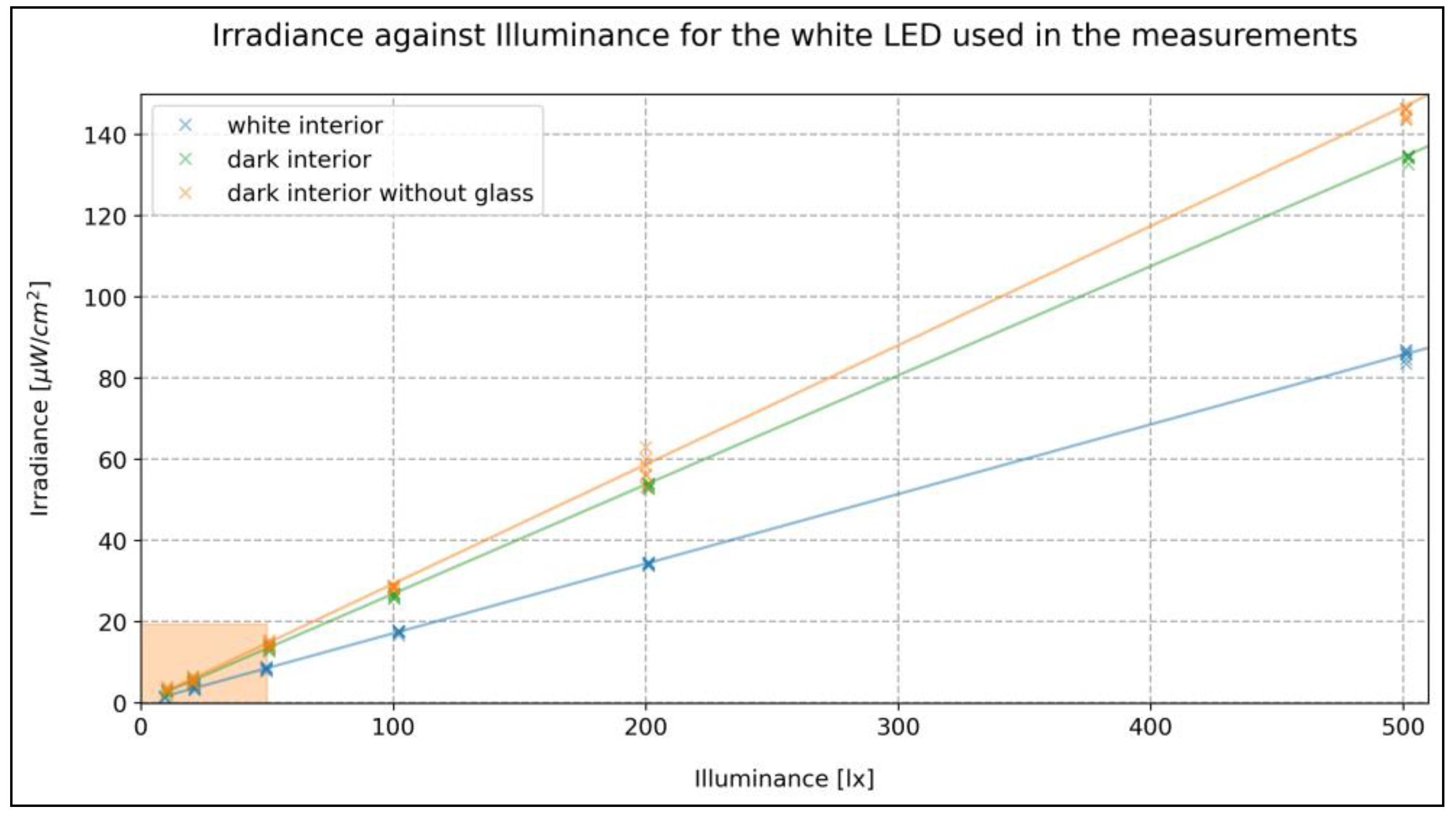
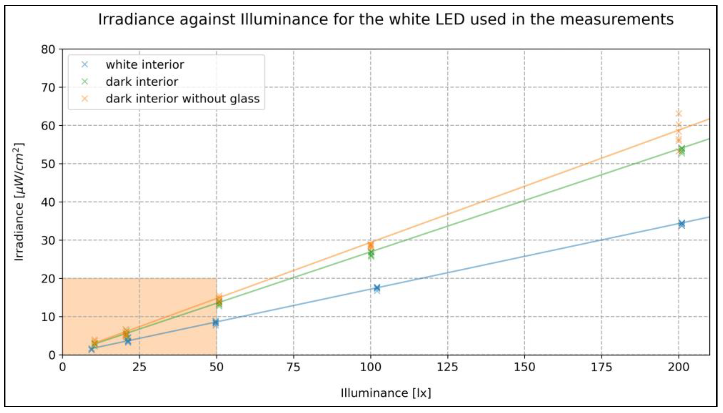
- Glass panel between LEDs and the measurement chamber, reflective walls (blue).
- Glass panel between LEDs and the measurement chamber darkened walls (green).
- No glass panel and darkened walls (orange).


| Marker 1 | Measurements between Markers | Marker 2 | ||||||
|---|---|---|---|---|---|---|---|---|
| Time | 04:52.459315 | Δ = 03:32.127744 | 08:24.587059 | |||||
| Avg | Min | Avg | Max | Peak to Peak | Charge/ Energy | Charge/ Energy | Avg | |
| V-SC | 2.132100662 V | 2.131851912 V | 3.171418731 V | 3.713132858 V | 1.581280947 V | --- | --- | 3.71262912 V |
| I-SC | 1.708 µA | 266 nA | 1.261 µA | 1.958 µA | 1.692 µA | 74 nA h | 267.424 µC | 495 nA |
| P-SC | 3.642 µW | 986 nW | 3.835 µW | 5.795 µW | 4.809 µW | 226 nW h | 813.539 µJ | 1.839 µW |
| V-MCU | 562.646319 mV | 449.552357 mV | 471.923875 mV | 585.626245 mV | 136.073887 mV | --- | --- | 470.835164 mV |
| I-MCU | 148 nA | −63 nA | 163 nA | 315 nA | 378 nA | 10 nA h | 34.665 µC | 161 nA |
| P-MCU | 84 nW | −35 nW | 77 nW | 148 nW | 184 nW | 5 nW h | 16.358 µJ | 76 nW |
| V-SENS | 2.082494775 V | 2.079386473 V | 3.121259748 V | 3.662744045 V | 1.583357573 V | --- | --- | 3.662415822 V |
| I-SENS | 157 nA | 31 nA | 201 nA | 11.95 µA | 11.92 µA | 12 nA h | 42.573 µC | 168 nA |
| P-SENS | 327 nW | 103 nW | 631 nW | 43.673 µW | 43.57 µW | 37 nW h | 133.816 µJ | 615 nW |
| Marker 1 | Measurements between Markers | Marker 2 | ||||||
|---|---|---|---|---|---|---|---|---|
| Time | 08:25.821594 | Δ = 390.758 ms Freq = 2.559 Hz | 08:26.212352 | |||||
| Avg | Min | Avg | Max | Peak to Peak | Charge/ Energy | Charge/ Energy | Avg | |
| V-SC | 3.713324308 V | 1.889625788 V | 3.308414034 V | 3.713439226 V | 1.823813438 V | --- | --- | 2.083846569 V |
| I-SC | 734 nA | 303 nA | 1.353 µA | 29.07 µA | 28.767 µA | 147 pA h | 529 nC | 1.716 µA |
| P-SC | 2.726 µW | 572 nW | 4.423 µW | 107.799 µW | 107.226 µW | 480 pW h | 1.728 µJ | 3.576 µW |
| V-MCU | 470.750034 mV | 470.456988 mV | 3.189349101 V | 3.575641632 V | 3.105184644 V | --- | --- | 961.210072 mV |
| I-MCU | 192 nA | 91 nA | 429.744 µA | 17.714757 mA | 17.714666 mA | 47 nA h | 167.926 µC | 141 nA |
| P-MCU | 90 nW | 69 nW | 1.176826 mW | 38.983947 mW | 38.983878 mW | 128 nW h | 459.855 µJ | 135 nW |
| V-SENS | 3.470034838 V | 2.026766777 V | 3.200025449 V | 3.471269131 V | 1.444502354 V | --- | --- | 2.038153887 V |
| I-SENS | 159 nA | −386 nA | 168 nA | 9.071 µA | 9.457 µA | 18 pA h | 66 nC | 189 nA |
| P-SENS | 550 nW | −815 nW | 546 nW | 31.442 µW | 32.257 µW | 59 pW h | 213 nJ | 386 nW |
| Marker 1 | Measurements between Markers | Marker 2 | ||||||
|---|---|---|---|---|---|---|---|---|
| Time | 337.437 ms | Δ = 536.5 ms Freq = 1.864 Hz | 873.938 ms | |||||
| Min | Avg | Max | Peak to Peak | Charge/Energy | Charge/Energy | |||
| V-SENS | 2.078642607 V | 2.067162514 V | 2.086894616 V | 2.103132963 V | 35.970449 mV | --- | --- | 2.097010374 V |
| I-SENS | 843 nA | −1.388 µA | 164 nA | 18.71 µA | 20.098 µA | 24 pA h | 88 nC | 558 nA |
| P-SENS | 1.753 µW | −2.894 µW | 342 nW | 39.035 µW | 41.929 µW | 51 pW h | 184 nJ | 1.17 µW |
| V-MCU | 833.948016 mV | 600.224555 mV | 652.319521 mV | 837.72999 mV | 237.505436 mV | --- | --- | 603.250086 mV |
| I-MCU | 350 nA | −1.7 µA | 151 nA | 1.622 µA | 3.321 µA | 23 pA h | 81 nC | 52 nA |
| P-MCU | 292 nW | −1.087 µW | 99 nW | 1.045 µW | 2.132 µW | 15 pW h | 53 nJ | 31 nW |
| Marker 1 | Measurements between Markers | Marker 2 | ||||||
|---|---|---|---|---|---|---|---|---|
| Time | −2.624 ms | Δ = 234.017 ms Freq = 4.273 Hz | 231.393 ms | |||||
| Min | Avg | Max | Peak to Peak | Charge/ Energy | Charge/ Energy | |||
| V-SENS | 1.562811852 V | 2.081658293 V | 2.198033571 V | 635.22172 mV | --- | --- | 2.070989132 V | |
| I-SENS | −35.098 µA | 10.4 µA | 92.915 µA | 128.013 µA | 669 pA h | 2.407 µC | 169 nA | |
| P-SENS | −76.179 µW | 21.634 µW | 145.209 µW | 221.387 µW | 1 nW h | 5.006 µJ | 349 nW | |
| V-MCU | 980.687022 mV | 1.989526746 V | 2.197713137 V | 1.217026114 V | --- | --- | 2.068371058 V | |
| I-MCU | −8.036295 mA | 55.084 µA | 187.327057 mA | 195.363352 mA | 4 nA h | 12.747 µC | 78 nA | |
| P-MCU | −13.461196 mW | 101.967 µW | 290.403066 mW | 303.864262 mW | 7 nW h | 23.595 µJ | 161 nW | |
References
- Market Research on Energy Harvesting for IoT Device. ConFlow Power. 2011. Available online: https://assets.website-files.com/6225ec4d016842cb92d1e5d3/629151680aab9776a55aaad2_Conflow-Energy-Harvesting-Report.pdf (accessed on 28 November 2022).
- Aileni, R.M.; Suciu, G.; Valderrama Sukuyama, C.A.; Pasca, S. Internet of Things and Communication Technology Synergy for Remote Services in Healthcare. In IoT and ICT for Healthcare Applications; Gupta, N., Paiva, S., Eds.; EAI/Springer Innovations in Communication and Computing; Springer: Cham, Switzerland; pp. 59–82. [CrossRef]
- Internet of Things (IoT) Connected Devices Installed Base Worldwide from 2015 to 2025. Statista. Available online: https://www.statista.com/statistics/471264/iot-number-of-connected-devices-worldwide/ (accessed on 28 November 2022).
- Komulainen, L.; Ruotsalainen, M. Billions of IoT Devices in the Field—Huge Negative Impact from Digitalization? Lappeenranta-Lahti University of Technology: Lahti, Finland, 2022. [Google Scholar] [CrossRef]
- Abdul-Qawy, A.S.H. Energy-Harvesting for IoT-based Wireless Nodes: A Progress Study. J. Soft Comput. Data Min. 2022, 3, 58–67. [Google Scholar] [CrossRef]
- Eshaghi, M.; Rashidzadeh, R. An Energy Harvesting Solution for IoT Sensors. In IEEE International Midwest Symposium on Circuits and Systems (MWSCAS); IEEE: New York, NY, USA, 2021; pp. 67–70. [Google Scholar] [CrossRef]
- Estrada-López, J.; Abuellil, A.; Zeng, Z.; Sanchez-Sinencio, E. Multiple Input Energy Harvesting Systems for Autonomous IoT End-Nodes. J. Low Power Electron. Appl. 2018, 8, 6. [Google Scholar] [CrossRef]
- Hidalgo-Leon, R.; Urquizo, J.; Silva, C.E.; Silva-Leon, J.; Wu, J.; Singh, P.; Soriano, G. Powering nodes of wireless sensor networks with energy harvesters for intelligent buildings: A review. Energy Rep. 2022, 8, 3809–3826. [Google Scholar] [CrossRef]
- Choudhary, P.; Bhargava, L.; Singh, V.; Choudhary, M.; Suhag, A.K. A survey—Energy harvesting sources and techniques for internet of things devices. Mater. Today Proc. 2020, 30, 52–56. [Google Scholar] [CrossRef]
- Recommended Lighting Levels in Buildings Archtoolbox. Available online: https://www.archtoolbox.com/recommended-lighting-levels/ (accessed on 28 November 2022).
- Luxmeter Chauvin Arnoux, CA-1110. Available online: https://www.chauvin-arnoux.ch/ca-1110.html (accessed on 28 November 2022).
- Meli, M.; Hegetschweiler, L. Affordable Energy Autonomous Wireless Sensor for Day and Night. In Proceedings of the Embedded World Conference, Nuremberg, Germany, 23–25 February 2016. [Google Scholar] [CrossRef]
- Kouzinopoulos, C.S.; Tzovaras, D.; Bembnowicz, P.; Meli, M.; Bellanger, M.; Kauer, M.; De Vos, J.; Pasero, D.; Schellenberg, M.; Vujicic, O. AMANDA: An Autonomous Self-Powered Miniaturized Smart Sensing Embedded System. In Proceedings of the 2019 IEEE 9th International Conference on Consumer Electronics (ICCE-Berlin), Berlin, Germany, 8–11 September 2019. [Google Scholar] [CrossRef]
- Michael, P.R.; Johnston, D.E.; Moreno, W. A Conversion Guide: Solar Irradiance and Lux Illuminance. J. Meas. Eng. 2020, 8, 153–166. [Google Scholar] [CrossRef]
- Charge and Use the SolarCell Remote of Your 2021 Samsung QLED TV. Available online: https://www.samsung.com/ca/support/tv-audio-video/tv-solarcell-remote/ (accessed on 28 November 2022).
- Mathews, I.; Kantareddy, S.N.; Buonassisi, T.; Peters, I.M. Technology and Market Perspective for Indoor Photovoltaic Cells. Joule 2019, 3, 1415–1426. [Google Scholar] [CrossRef]
- LEH3—Product Brief. Epishine. Available online: https://4883108.fs1.hubspotusercontent-na1.net/hubfs/4883108/60e2f318bf114d29ba5c714d_LEH3%20Product%20Brief.pdf (accessed on 28 November 2022).
- Epishine. Indoor Light Energy Harvesting. Available online: https://www.epishine.com/product (accessed on 28 November 2022).
- TDK. Information about the BCS4430B6 BCS Series. Available online: https://product.tdk.com/system/files/dam/doc/product/solar-cell/catalog/film-solarcell_bcs_en.pdf (accessed on 28 November 2022).
- Lightricity. Datasheet of EXL1-1V20 Solar Cell Module. Available online: https://lightricity.co.uk/excelllight-exl1-1v20 (accessed on 28 November 2022).
- Juang, S.S.; Lin, P.Y.; Lin, Y.C.; Chen, Y.S.; Shen, P.S.; Guo, Y.L.; Wu, Y.C.; Chen, P. Energy Harvesting Under Dim-Light Condition with Dye-Sensitized and Perovskite Solar Cells. Front Chem. 2019, 7, 209. [Google Scholar] [CrossRef] [PubMed]
- Biswas, S.; Kim, H. Solar Cells for Indoor Applications: Progress and Development. Polymers 2020, 12, 1338. [Google Scholar] [CrossRef] [PubMed]
- Li, B.; Amaratunga, G.A.J. Indoor photovoltaics, the Next Big Trend in solution-processed solar cells. InfoMat 2021, 3, 445–459. [Google Scholar] [CrossRef]
- Mathews, I.; Kelly, G.; King, P.J.; Frizzell, R. GaAs solar cells for Indoor Light Harvesting. In Proceedings of the IEEE 40th Photovoltaic Specialist Conference (PVSC), Denver, CO, USA, 8–13 June 2014. [Google Scholar] [CrossRef]
- Lee, H.G.; Chang, N. Powering the IoT: Storage-less and converter-less energy harvesting. In Proceedings of the 20th Asia and South Pacific Design Automation Conference, Chiba, Japan, 19–22 January 2015. [Google Scholar] [CrossRef]
- Riaz, A.; Sarker, M.R.; Saad, M.H.M.; Mohamed, R. Review on Comparison of Different Energy Storage Technologies Used in Micro-Energy Harvesting, WSNs, Low-Cost Microelectronic Devices: Challenges and Recommendations. Sensors 2021, 21, 5041. [Google Scholar] [CrossRef] [PubMed]
- Baek, D.; Lee, H.G.; Chang, N. SmartPatch: A Self-Powered and Patchable Cumulative UV Irradiance Meter. IEEE Des. Test 2019, 36, 57–64. [Google Scholar] [CrossRef]
- Meli, M.; Roth, N.; Gutzwiller, P. Wireless sensing using LEDs as very low-cost energy harvesters. In Proceedings of the Embedded World Conference, Nuremberg, Germany, 24–26 February 2015. [Google Scholar] [CrossRef]
- Yue, X.; Kauer, M.; Bellanger, M.; Beard, O.; Brownlow, M.; Gibson, D.; Clark, C.; MacGregor, C.; Song, S. Development of an Indoor Photovoltaic Energy Harvesting Module for Autonomous Sensors in Building Air Quality Applications. IEEE Internet Things J. 2017, 4, 2092–2103. [Google Scholar] [CrossRef]
- Wu, F.; Redouté, J.-M.; Yuce, R. A Self-Powered Wearable Body Sensor Network System for Safety Applications. In Proceedings of the 2018 IEEE SENSORS, New Delhi, India, 28–31 October 2018. [Google Scholar] [CrossRef]
- Pubill, D.; Serra, J.; Verikoukis, C. Harvesting artificial light indoors to power perpetually a Wireless Sensor Network node. In Proceedings of the 2018 IEEE 23rd International Workshop on Computer Aided Modeling and Design of Communication Links and Networks (CAMAD), Barcelona, Spain, 17–19 September 2018. [Google Scholar] [CrossRef]
- Kantareddy, S.N.R.; Mathews, I.; Sun, S.; Layurova, M.; Thapa, J.; Correa-Baena, J.-P.; Bhattacharyya, R.; Buonassisi, T.; Sarma, S.E.; Peters, I.A. Perovskite PV-Powered RFID: Enabling Low-Cost Self-Powered IoT Sensors. IEEE Sens. J. 2020, 20, 471–478. [Google Scholar] [CrossRef]
- Perovskite PV-Powered RFID: Enabling Low-Cost Self-Powered IoT Sensors. Available online: https://www.youtube.com/watch?v=d6BmzFla6t4 (accessed on 29 November 2022).
- Michaels, H.; Rinderle, M.; Freitag, R.; Benesperi, I.; Edvinsson, T.; Socher, R.; Gagliardi, A.; Freitag, M. Dye-sensitized solar cells under ambient light powering machine learning: Towards autonomous smart sensors for the internet of things. Chem. Sci. 2020, 11, 2895–2906. [Google Scholar] [CrossRef] [PubMed]
- Rosa, R.L.; Dehollain, C.; Burg, A.; Costanza, M.; Livreri, P. An Energy-Autonomous Wireless Sensor with Simultaneous Energy Harvesting and Ambient Light Sensing. IEEE Sens. J. 2021, 21, 13744–13752. [Google Scholar] [CrossRef]
- Mishu, M.K.; Rokonuzzaman, M.; Pasupuleti, J.; Shakeri, M.; Rahman, K.S.; Binzaid, S.; Tiong, S.K.; Amin, N. An Adaptive TE-PV Hybrid Energy Harvesting System for Self-Powered IoT Sensor Applications. Sensors 2021, 21, 2604. [Google Scholar] [CrossRef] [PubMed]
- Elsys. Sensing Tomorrow. Available online: https://www.elsys.se/en/ (accessed on 29 November 2022).
- Meli, M.; Brütsch, M.; Stajic, S.; Böbel, M.; Lorenz, D.; Hegetschweiler, L.; Karanassos, D.; Kouzinopoulos, C. Low Light Energy Autonomous LoRaWAN Node. In Proceedings of the 2020 IEEE 5th International Symposium on Smart and Wireless Systems within the Conferences on Intelligent Data Acquisition and Advanced Computing Systems (IDAACS-SWS), Dortmund, Germany, 17–18 September 2020. [Google Scholar] [CrossRef]
- Vračar, L.; Prijić, A.; Nešić, D.; Dević, S.; Prijić, Z. Photovoltaic Energy Harvesting Wireless Sensor Node for Telemetry Applications Optimized for Low Illumination Levels. Electronics 2016, 5, 26. [Google Scholar] [CrossRef]
- Lin, L.; Jain, S.; Alioto, M. Multi-Sensor Platform with Five-Order-of-Magnitude System Power Adaptation down to 3.1nW and Sustained Operation under Moonlight Harvesting. In Proceedings of the IEEE Symposium on VLSI Circuits, Honolulu, HI, USA, 16–19 June 2020. [Google Scholar] [CrossRef]
- Librizzi, F. When to use a standalone RTC IC instead of an MCU embedded RTC in low power IoT devices. Power Electronics News. 2019. Available online: https://www.powerelectronicsnews.com/when-to-use-a-standalone-rtc-ic-instead-of-an-mcu-embedded-rtc-in-low-power-iot-devices/ (accessed on 12 January 2023).
- NXP. Datasheet of the PCF2131. Available online: https://www.nxp.com/docs/en/data-sheet/PCF2131DS.pdf (accessed on 20 January 2023).
- Epson. Datasheet of RX-8731LC. Available online: https://www5.epsondevice.com/en/products/rtc/rx8731lc.html (accessed on 20 January 2023).
- Ambiq. Information and Links to Datasheets of RTCs. Available online: https://ambiq.com/rtc/ (accessed on 20 January 2023).
- Texas Instruments. Datasheet of TPL5100. Available online: https://www.ti.com/lit/ds/symlink/tpl5100.pdf (accessed on 20 January 2023).
- Microchip. Low Power Touch Design. Available online: https://ww1.microchip.com/downloads/en/Appnotes/AN2812-Low-Power-Touch-Design-00002812B.pdf (accessed on 21 January 2023).
- Renesas. Realizing Low Power Consumption of the Capacitive Touch Sensors with RX140! Available online: https://www.renesas.com/tw/en/blogs/realizing-low-power-consumption-capacitive-touch-sensors-rx140 (accessed on 21 January 2023).
- SiLabs. AN507; Low Power Capacitive Sensing. Available online: https://www.silabs.com/documents/public/application-notes/AN507.pdf (accessed on 21 January 2023).
- Hussaini, S.; Jiang, H.; Walsh, P.; MacSweeney, D.; Makinwa, K.A.A. A 15nW Per Button Noise-Immune Readout IC for Capacitive Touch Sensor. In Proceedings of the IEEE 44th European Solid State Circuits Conference (ESSCIRC), Dresden, Germany, 3–6 September 2018. [Google Scholar] [CrossRef]
- EM Microelectronic Marin. Datasheet of EM6420 Touch Sensor. Available online: https://www.emmicroelectronic.com/sites/default/files/products/datasheets/em6420_ds.pdf (accessed on 21 January 2023).
- Aiello, O.; Crovetti, P.; Alioto, M. Wake-Up Oscillators with pW Power Consumption in Dynamic Leakage Suppression Logic. In Proceedings of the IEEE International Symposium on Circuits and Systems (ISCAS), Sapporo, Japan, 26–29 May 2019. [Google Scholar] [CrossRef]
- Torrisi, A.; Yıldırım, K.S.; Brunelli, D. Ultra-Low-Power Circuits for Intermittent Communication. J. Low Power Electron. Appl. 2022, 12, 60. [Google Scholar] [CrossRef]
- Epishine. Indoor Light Energy Harvesting (Check for LEH3—Data Sheet). Available online: https://www.epishine.com/product (accessed on 29 November 2022).
- EM Microelectronic Marin. Power Management Controller (Datasheet of the EM8500). Available online: https://www.emmicroelectronic.com/sites/default/files/products/datasheets/8500-ds.pdf (accessed on 29 November 2022).
- E-Peas. Datasheet of AEM10941. Available online: https://e-peas.com/wp-content/uploads/2022/09/e-peas-AEM10941-datasheet-solar-energy-harvesting.pdf (accessed on 29 November 2022).
- Brütsch, M.; Brülisauer, C.; Widmer, L.; Kräuchi, R.; Truninger, D.; Meli, M. Comparing the energy requirements of bluetooth smart devices. In Proceedings of the Wireless Congress, WEKA, Munich, Germany, 14–15 November 2018. [Google Scholar] [CrossRef]
- Lightricity. Outdoor & Space Products (Some Technology Information). Available online: https://lightricity.co.uk/outdoor-%26-space-products (accessed on 29 November 2022).
- Lightricity. Technology. Available online: https://lightricity.co.uk/technology (accessed on 21 January 2023).
- Information About the Comparator is Available from Microdul AG Under Agreement. Available online: https://ec.europa.eu/research/participants/documents/downloadPublic?documentIds=080166e5ca68bca1&appId=PPGMS (accessed on 28 November 2022).
- Micro Crystal. RV-3028-C7 (Main Page for the RTC Module). Available online: https://www.microcrystal.com/en/products/real-time-clock-rtc-modules/rv-3028-c7/ (accessed on 29 November 2022).
- Micro Crystal. Datasheet of the RTC Module. Available online: https://www.microcrystal.com/fileadmin/Media/Products/RTC/Datasheet/RV-3028-C7.pdf (accessed on 29 November 2022).
- Micro Crystal. Application Manual RV-3028-C7. Available online: https://www.microcrystal.com/fileadmin/Media/Products/RTC/App.Manual/RV-3028-C7_App-Manual.pdf (accessed on 29 November 2022).
- Microdul. MS8892B Preliminary Datasheet. Available online: https://www.microdul.com/en/assets/public/images/content/MS8892B_Datasheet_M90-32-0632.pdf (accessed on 29 November 2022).
- Onsemi. Bluetooth 5.2 Radio System-on-Chip (SoC). Available online: https://www.onsemi.com/pdf/datasheet/rsl10-d.pdf (accessed on 29 November 2022).
- Onsemi. Bluetooth 5.2 System-in-Package (SiP). Available online: https://www.onsemi.com/pdf/datasheet/rsl10sip-d.pdf (accessed on 29 November 2022).
- Onsemi. RSL10-SIP-001GEVB Development Board (User’s Manual). Available online: https://www.onsemi.com/pub/collateral/evbum2565-d.pdf (accessed on 29 November 2022).
- Keysight. N6700 Modular Power System Family (Information about N678xA Power Analyser). Available online: https://www.keysight.com/us/en/assets/7018-05460/data-sheets/5992-1880.pdf (accessed on 29 November 2022).
- MAVOLUX 5032 B USB This high Precision Luxmeter (Description of Mavolux 5032B USB Luxmeter). Available online: https://gossen-photo.de/en/mavolux-5032-b-usb-2/ (accessed on 29 November 2022).
- Texas Instruments. TIDC-CC2650STK-SENSORTAG (CC2650 SensorTag Used as BLE Sniffer). Available online: https://www.ti.com/tool/TIDC-CC2650STK-SENSORTAG (accessed on 29 November 2022).
- High-Sensitivity Irradiance Measurement Kit. Available online: https://dyenamo.se/analytical_equipment_DN-AE06.php (accessed on 21 January 2023).


| Illuminance (Lux) | 2 | 4 | 10 | 19 | 50 | 100 | 200 | 500 |
|---|---|---|---|---|---|---|---|---|
| Power (µW) | 0.52 | 1.05 | 2.62 | 5.15 | 14.92 | 29.73 | 63.13 | 162.2 |
| Load (kOhm) | 17,000 | 9500 | 4100 | 2200 | 850 | 440 | 230 | 95 |
| Voltage at MPP (V) | 2.96 | 3.15 | 3.28 | 3.37 | 3.56 | 3.62 | 3.81 | 3.93 |
| M1 | Measurements between Markers | M2 | ||||
|---|---|---|---|---|---|---|
| Time | 3.339715 s | Δ = 09:36.688620 (576.688 s) | 09:40.028334 | |||
| Avg | Min | Avg | Max | Energy | Avg | |
| V-SC | 2.54 mV | 1.03 mV | 1.28 V | 2.25 V | - | 2.25 V |
| I-SC | 652 nA | 246 nA | 475 nA | 754 nA | - | 345 nA |
| P-SC | 2 nW | 558 pW | 566 nW | 1.14 µW | 326.33 µJ | 776 nW |
| M1 | Measurements between Markers | M2 | ||||
|---|---|---|---|---|---|---|
| Time | 09:40.398940 | Δ = 11:06.243236 (666.243 s) | 20:46.642176 | |||
| Avg | Min | Avg | Max | Energy | Avg | |
| V-SC | 2.05 V | 2.05 V | 2.42 V | 2.68 V | - | 2.68 V |
| I-SC | 406 nA | 177 nA | 354 nA | 535 nA | - | 288 nA |
| P-SC | 834 nW | 468 nW | 856 nW | 1.26 µW | 570.04 µJ | 771 nW |
| M1 | Measurements between Markers | M2 | ||||
|---|---|---|---|---|---|---|
| Time | 20:48.623002 | Δ = 03:50.908887 (230.908 s) | 24:39.531889 | |||
| Avg | Min | Avg | Max | Energy | Avg | |
| V-SC | 1.44 V | 1.44 V | 1.89 V | 2.25 V | - | 2.25 V |
| I-SC | 430 nA | 249 nA | 408 nA | 583 nA | - | 344 nA |
| P-SC | 618 nW | 462 nW | 765 nW | 1.13 µW | 176.65 µJ | 774 nW |
| M1 | Measurements between Markers | M2 | ||||
|---|---|---|---|---|---|---|
| Time | 09:40.398940 | Δ = 11:06.243236 (666.243 s) | 20:46.642176 | |||
| Avg | Min | Avg | Max | Energy | Avg | |
| V-SC | 2.06 V | 2.06 V | 2.30 V | 2.49 V | - | 2.49 V |
| I-SC | 345 nA | 205 nA | 367 nA | 547 nA | - | 319 nA |
| P-SC | 710 nW | 460 nW | 841 nW | 1.21 µW | 293.89 µJ | 794 nW |
| 2 Lux | 5 Lux | 10 Lux | 20 Lux | |
|---|---|---|---|---|
| Start time 1 | 04:24.488141 | 03:20.915354 | 01:49.326336 | 01:07.183411 |
| Duration 2 | 10:14.418022 | 05:55.556065 | 02:50.100326 | 01:20.592077 |
| P-SC Min | 212 nW | 382 nW | 749 nW | 1.567 µW |
| P-SC Avg | 436 nW | 702 nW | 1.374 µW | 2.758 µW |
| P-SC Max | 731 nW | 1.145 µW | 2.113 µW | 4.13 µW |
| I-SC Min | 98 nA | 236 nA | 589 nA | 1.422 µA |
| I-SC Avg | 268 nA | 435 nA | 855 nA | 1.719 µA |
| I-SC Max | 451 nA | 651 nA | 1.107 µA | 2.029 µA |
| SC energy 3 | 267.68 µJ | 249.578 µJ | 233.778 µJ | 222.256 µJ |
| Extra energy 4 | 75.68 µJ | 57.578 µJ | 41.778 µJ | 30.256 µJ |
| Cold start time 5 | 878 s | 556 s | 279 s | 147 s |
Disclaimer/Publisher’s Note: The statements, opinions and data contained in all publications are solely those of the individual author(s) and contributor(s) and not of MDPI and/or the editor(s). MDPI and/or the editor(s) disclaim responsibility for any injury to people or property resulting from any ideas, methods, instructions or products referred to in the content. |
© 2023 by the authors. Licensee MDPI, Basel, Switzerland. This article is an open access article distributed under the terms and conditions of the Creative Commons Attribution (CC BY) license (https://creativecommons.org/licenses/by/4.0/).
Share and Cite
Meli, M.L.; Favre, S.; Maij, B.; Stajic, S.; Boebel, M.; Poole, P.J.; Schellenberg, M.; Kouzinopoulos, C.S. Energy Autonomous Wireless Sensing Node Working at 5 Lux from a 4 cm2 Solar Cell. J. Low Power Electron. Appl. 2023, 13, 12. https://doi.org/10.3390/jlpea13010012
Meli ML, Favre S, Maij B, Stajic S, Boebel M, Poole PJ, Schellenberg M, Kouzinopoulos CS. Energy Autonomous Wireless Sensing Node Working at 5 Lux from a 4 cm2 Solar Cell. Journal of Low Power Electronics and Applications. 2023; 13(1):12. https://doi.org/10.3390/jlpea13010012
Chicago/Turabian StyleMeli, Marcel Louis, Sebastien Favre, Benjamin Maij, Stefan Stajic, Manuel Boebel, Philip John Poole, Martin Schellenberg, and Charalampos S. Kouzinopoulos. 2023. "Energy Autonomous Wireless Sensing Node Working at 5 Lux from a 4 cm2 Solar Cell" Journal of Low Power Electronics and Applications 13, no. 1: 12. https://doi.org/10.3390/jlpea13010012