Article

Expanding Plasma Process for Nitriding Mo–Ti Bilayer Thin Films

1
Faculté des Sciences et Techniques, Université de Limoges, CNRS, UMR7315, IRCER, CEC, 12 Rue Atlantis, F-87068 Limoges, France
2
Institut Jean Lamour, CNRS, UMR7198, Université de Lorraine, Site ARTEM, 2 allée A. Guinier, F-54011 Nancy, France
3
Faculté des Sciences et Techniques, Université de Limoges, CNRS, XLIM, UMR6172, 123 av. A. Thomas, F-87060 Limoges, France
*
Author to whom correspondence should be addressed.
Coatings 2019, 9(2), 96; https://doi.org/10.3390/coatings9020096
Submission received: 14 December 2018 / Revised: 21 January 2019 / Accepted: 31 January 2019 / Published: 5 February 2019

Abstract

:
Owing to the reducing effect of NHx radicals and H species produced in (Ar-N2-H2) expanding plasma, chemical reactions are promoted in thin metal films in contrast with other plasma treatments where the impinging energetic ions play the main role. Multi layers of Mo, Ti, and their nitrides are used in very recent applications such as supercapacitors or solar cells. They combine the interesting properties of the constituents. This work reports on the formation and the structure of Ti nitrides and Mo silicides in Mo–Ti bilayer films coated on Si wafers exposed to (Ar-N2-H2) plasma for 1 to 3 h. Nitrogen diffuses into the surface layers from 400 °C and TiN starts to crystallize from 600 °C. Interdiffusion of Mo, Ti, and Si through Mo–Ti bilayer films gives rise to the formation of Mo–Ti alloys and MoSi2 of hexagonal structure, which transforms into MoSi2 of tetragonal structure at longer treatment durations. A 1 h 30 min plasma exposure at 800 °C leads to the formation of three layers of nearly equal thickness with clear interfaces, which consist of TiN and MoSi2 of nanometric size in the vicinity of the Mo–Ti bilayer film surface.

1. Introduction

Transition metal nitrides and silicides exhibit very attractive physical and chemical properties. Owing to their structure which involves covalent, ionic, and metallic bonding, the high hardness, Young modulus, and melting point equal to 2947 °C for TiN, make them similar to ceramic materials, whereas their low electrical resistivity equal to 19.8 μΩ·cm for Mo2N and 30 μΩ·cm for TiN make them similar to metals [1,2,3]. In the same way, transition metal silicides also exhibit low resistivity equal to 14–17 μΩ·cm for TiSi2 [4]. A low value of about 40 μΩ·cm has also been found for molybdenum silicide films with Si/Mo ratio equal to about 1 [5]. Transition metal silicides also have high temperature stability, chemical compatibility, and low Schottky barrier height. Transition metal nitrides and silicides are used in a large range of applications. They can replace conventional polysilicon as gate electrodes and interconnects in metal oxide semiconductor (MOS) devices [6]. The barrier height of TiN/TiSix/Si systems is lowered by 80 meV compared with TiSix/Si Schottky diodes, which results in 15% of self-power consumption saving [7]. Multilayer films of transition metal nitrides, with layer thickness ranging from ten to hundreds of nanometers, allow beneficial properties of constituting materials to be combined [8]. Ti–Mo multilayers have attracted much interest in a wide range of applications. MoNx/TiN systems have been recently investigated for their enhanced electron transportation capability, capacitance, and high cycling stability which make them valuable as supercapacitor electrode material for energy storage [9,10]. TiN films are also good diffusion barrier layers. High efficiency CIGS (Cu(In,Ga)Se2) solar cells can be obtained by introducing a thin TiN film between Mo back electrode and the soda lime glass substrate [11,12]. TiN films prevent Na diffusion from the soda lime glass into the CIGS absorber via the Mo contact [12].
Films of metal nitrides are mainly deposited by vacuum arc evaporation [8], direct current (DC) or radio frequent (RF) magnetron reactive sputtering [6,11]. A review of deposition methods of thin films is reported in [2]. In this work, the thermochemical treatment of thin metal films is carried out in expanding plasma of (Ar-N2-H2) gas mixtures activated by microwaves of 2.45 GHz. The high degree of ionization and dissociation makes the microwave plasma very attractive compared with other types of electrical excitations. In contrast with most plasma treatments, the sputtering of the surface of materials by the impinging energetic ions, as well as the heating effect, is trifling. The reducing effect of passive surface layers, which remain on materials such as oxides and carbides, is carried out by hydrogen species such as NHx and/or H produced in (Ar-N2-H2) plasma. This process promotes chemical reactions on the surface of metal films. A reduction-nitridation process has been evidenced in Mo thin films processed in expanding plasma [13]. Exothermic reactions produced between hydrogen species and oxides remaining in Mo film, promote the formation of the high temperature γMo2N phase to the detriment of the low temperature βMo2N phase. In the same way, a competing process leading to the gradual conversion of TiSi2 into TiN, in accordance with the values of the respective enthalpy of formation, has been investigated in Ti thin films exposed to (Ar-N2-H2) plasma [14]. In this work, the formation of nitrides and silicides in Mo–Ti bilayer films is analyzed by way of various investigation means. This work is especially focused on the crystallization and growth of various phases such as Ti nitrides and Mo silicides due to the intensive diffusion of N, Si, Ti, and Mo through the Mo–Ti bilayer films. The results are compared with those previously obtained in Mo and Ti thin films.

2. Materials and Methods

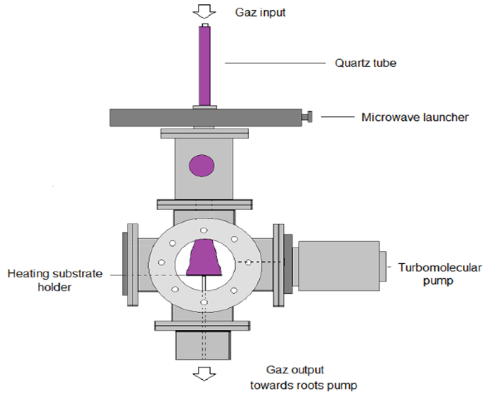
2.1. Conditions of Formation of an Expanding Plasma

The experiments are carried out in the reactor displayed in Figure 1.
The plasma is ignited in (Ar-N2-H2) gas mixtures by a microwave discharge which is produced by means of a SAIREM GMP 12 kE power supply operating up to 1.2 kV at a frequency of 2.45 GHz in a fused silica tube (external and internal diameter of 24 and 20 mm, respectively) passing through the surface wave launcher. The power of the electromagnetic wave is mainly transferred to electrons and then to other gaseous species by collisions. The plasma is expanded out of the center of the discharge into the stainless steel vessel up to the surface of the substrate, under the conditions of a high density of electrons. These conditions depend on the microwave frequency as well as the frequency of collisions occurring in the plasma. The electron density is equal to 1.68 × 10¹⁶ m−3 in pure Ar plasma at 2 cm from the discharge tube exit, at a microwave power of 400 W [13]. The addition of molecular gas in Ar results in a decrease of electron density with increasing collisions between electrons and molecules. The electron density is about 5 times lower in (Ar-50%N2) and pure N2 plasma. It is equal to about 2.78 × 10¹⁴ m−3 in (Ar-31%N2-6%H2) plasma used in this study. The electron density tends to decrease at a larger distance from the discharge tube exit. (Ar-N2-H2) plasma mainly produce Ar+ ions and reactive species such as NHx radicals. The density of Ar is equal to about 2 × 10²² m−3. This value is about 100 times larger than those of NH3 and NH2 radicals and about 103 and 104 larger than NH and N radicals. The flux of Ar+ ions is equal to about 7 × 10¹⁸ m2·s−1. The electron and ion energies are equal to 0.51–1.37 eV and 0.1 eV, respectively. Since the ion energy is very low, plasma species such as NHx and H species play the main role during the process. They react at the surface of the substrate and thus promote the transfer of active species into the surface layers. Under the condition of wave propagation, the plasma expanded out of the center of the discharge forms a bright cone from the quartz tube exit up to the heating substrate holder (Figure 1). The plasma treatment process is optimized by moving the substrate holder relative to the center of the discharge along the vertical axis. In this work, the experiments are made in (Ar-31%N2-6%H2) at 12.5 cm from the center of the discharge at a microwave power of 500 W.

2.2. Deposition of Thin Films

Mo and Ti films are successively deposited on Si(100) wafers in an electron beam evaporator filled with Ar gas (alphagas N50 H2O < 3 ppm, O2 < 2 ppm and CnHm < 0.5 ppm) at a pressure of 0.5 Pa. Pure Mo and Ti cylinders and pellets (99.95%) are used. Si wafers are biased at −400 V and heated at 400 °C. Under such conditions, the surface is cleaned by impinging ions that improve the adhesion of films on substrates. The thickness of Mo and Ti films, equal to 250 nm each, is controlled by a quartz balance. The resulting samples of final dimensions equal to about 10 × 10 mm2 are cut from wafers.

2.3. Plasma Nitriding Process

Mo–Ti bilayer films are placed on the heating substrate holder. The vacuum chamber is then evacuated to a pressure of 10−5 Pa. The heating is switched on up to 400, 600, and 800 °C. Once the temperature is reached, (Ar-31%N2-6%H2) gas mixture is introduced into the chamber. The discharge is produced at a microwave power of 500 W and a total pressure of 0.13 kPa. The experiments are run for 1 h, 1 h 30 min, and 3 h.

2.4. Investigations of Mo–Ti Bilayer Films

The phase composition and crystal structures of the compounds are examined by X-ray diffraction (XRD) and Raman spectroscopy. XRD measurements are carried out in a D8 Advance Bruker diffractometer (Karlsruhe, Germany) using a primary monochromator to select CuKα1 radiation and a Lynx-eye position sensitive detector (3.4° for fast acquisition). The configuration of the system is the classical Bragg-Brentano geometry. Raman spectra are recorded in backscattering geometry by using a HORIBA-JOBIN-YVON T 64000 model spectrometer (Villeneuve d’Ascq, France), equipped with a charged coupled device (CCD) camera cooled by a flux of liquid N2 up to −133 °C, to reduce thermal noise. The exciting line, of a wavelength equal to 514.532 nm, is produced by an Ar+ laser and focused onto the sample, via a ×50-long working distance objective, resulting in a spot of diameter equal to 1 μm. The power of the laser is modified to protect the sample from any damage. The spectra are averaged to make the signal intensities representative of the samples. The diffusion profiles of elements are established by secondary ion mass spectrometry (SIMS) in an IMS7F CAMECA spectrometer (Gennevilliers, France), which is conducted using cesium ions (Cs+) with a primary voltage and intensity of 5 kV and 25 nA, respectively. The primary beam is scanned over an area of 200 μm × 200 μm. The results are normalized with respect to the cesium signal. The structure, the crystalline phases, interfaces, and microstructures are investigated by transmission electron microscopy (TEM) and selected area electron diffraction (SAED) in a 2100F JEOL microscope (Tokyo, Japan). Chemical composition of films are analyzed by nano-probe energy dispersive spectrometry (EDS) in the 2100F JEOL microscope (Tokyo, Japan). Cross sectional samples are prepared by mechanical polishing and subsequently thinned by argon ion milling, before they are analyzed. The morphology of the surface is measured by means of scanning electron microscopy (SEM) in a Zeiss crossbeam 550 model (GmbH, Oberkochen, Germany).

3. Results

3.1. Mo–Ti Interface Formation of Mo–Ti Solid Solution

The X-ray diffraction pattern corresponding to the untreated Mo–Ti film only displays the most intense reflection lines of atomic planes of pure Mo of body-centered cubic structure at 2θ Bragg angles equal to 40.52° and 73.68° (JCPDS card no. 42.1120) (Figure 2).
No trace of Ti metal is detected. The other intense diffraction peak at 69° corresponds to the Si substrate (JCPDS card no. 01-7247). Previous investigations performed on pure Ti thin films coated on Si wafers, and using the same method, resulted in XRD patterns displaying the features of Ti of hexagonal-close packed structure. The most intense diffraction line is close to the one of Mo at 40.52°. However, since the peak assigned to Mo seems quite symmetrical, we can conclude that Ti does not crystallize in hexagonal structure in Ti–Mo bilayer films and/or Mo is much more crystallized than Ti. The second assumption is consistent with a recent study. Xin et al. [16] have deposited a Ti–Mo bilayer on Al2O3 ceramic by magnetron sputtering. The thicknesses of Mo and Ti films are close to those that were used in the present work. The corresponding XRD pattern reported in [16] only shows a tiny peak corresponding to Ti of hexagonal structure close to a very intense Mo peak. The large intensity difference has been assigned to a better crystallization of Mo. In the present work, a thorough examination of the XRD pattern (Figure 2) allows us to see a tiny peak located at a Bragg angle equal to about 39.1°. It is worth noting that pure Ti crystallizes in another allotropic form of body-centered cubic structure similar to Mo, which is named β-phase, in contrast with α-phase of hexagonal structure, stable at room temperature. The transformation of the α-phase into β-phase occurs at 1155 K [17]. However, the addition of Mo promotes the stability of the β-phase at room temperature. Mo is slightly soluble in α-Ti, whereas β-Ti forms a continuous series of solid solutions with Mo, according to the Mo–Ti phase diagram [18]. The microstructure of Ti varies with Mo content: The α-phase of low Mo content consists of an arrangement of regular lamellae, whereas the β-phase is identified as an arrangement of large grains. The Bragg angle 2θ = 39.1° corresponds to the most intense reflection line of Ti0.9Mo0.1 solid solution of body-centered cubic structure, with a lattice parameter a = 0.3257 nm (JCPDS card no. 04-018-6034). In their very recent article, Kislitin et al. 2018 [19] fitted the lattice parameter of β-Ti–Mo solid solutions versus at.% of Mo to a Vegard’s law. They found a strong negative departure of the function compared to the Vegard’s law which is assigned to a strong lattice compression. According to Vegard’s law, the lattice parameter of 0.325 nm should correspond to a Mo content of about 35 at.%. The formation of Ti0.9Mo0.1 solid solution is consistent with other results found in the literature, since it is reported that Ti–Mo solid solutions, with Mo content larger than 8–10 at.%, crystallize in β-Ti structure with an intense reflection line at about 39°. The other XRD peaks are only slightly intense [20,21,22].
So, we can conclude that the lack of α-Ti phase in XRD patterns can be correlated to the formation of β-Ti-Mo alloys, during the deposition of Mo–Ti bilayers on Si wafers by evaporation. However, the growth of epitaxial Ti films on Mo surface or TiO2 cannot be ruled out. In what follows, investigations on the diffusion profiles corresponding to elements contained in Ti–Mo bilayers and carried out by SIMS, will help us to clear up this phenomenon. Owing to the high sensitivity and excellent separation power of SIMS method, the evolution of the SIMS signal of various elements contained in films versus process temperature is well identified. Quantitative analysis may only be conducted through relative measurements by using a calibration factor for most elements. The diffusion profiles of Si, Ti, Mo, C, N, and O are displayed in Figure 3.
The Mo–Si interface is well identified for a sputtering time of about 800 s. The Mo–Ti interface is still identified; however, Ti has diffused into the whole Mo film thickness up to the Mo–Si interface. So, Mo–Ti alloys are formed. Such a result was obtained in a recent study on the formation of a Mo–Ti layer with a Ti content gradient, in Ti/Mo/Yb0.3Co4Sb12 thermoelectric joints heated at 550 °C in vacuum [23]. As also seen in Figure 3, the nitrogen and carbon signals are low in the as-deposited Ti–Mo bilayer. In contrast, the oxygen signal is high. Oxygen has been incorporated in the Ti–Mo bilayer during the evaporation of metals. Since Ti is very reactive towards oxygen, the formation of TiO2 of amorphous structure, in addition to Mo–Ti alloys, can be expected during the evaporation process.
In what follows, the formation and growth of TiN and MoSi2 crystallized phases in Mo–Ti bilayer films coated on Si substrates, heated at 600 and 800 °C and exposed to (Ar-31%N2-6%H2) plasma for 1 h 30 min and 3 h, have been investigated by XRD and Raman spectroscopy.

3.2. Formation of TiN and MoSi2 in Mo–Ti Bilayer Films Processed in Expanding Plasma

3.2.1. XRD Investigations

TiN starts to crystallize at 600 °C. The tiny features detected at Bragg angles of 36.8° and 42.6° are assigned to the most intense (111) and (200) reflection lines of the TiN phase of cubic structure (JCPDS card no. 04-004-2917) (Figure 4a).
Since the XRD peaks are broad and slightly intense, TiN consists of small crystallites. The other reflection lines located at Bragg angles equal to 25° and 43° correspond to the anatase phase of TiO2. Compared with TiN, TiO2 is well crystallized. Ti metal, which strongly reacts with oxygen to form TiO2 of amorphous structure during the evaporation process, crystallizes during the plasma process. A longer exposure time up to 3 h results in a decrease of both TiN and TiO2 reflection line intensities (Figure 4b). Hydrogen species as NHx radicals and/or H atoms produced in (Ar-N2-H2) plasma have a reducing effect on oxide species, which form in the surface layers of metal films such as Ti [15]. However, as far as TiN is concerned, hydrogen species could also have an etching effect on TiN during the first stages of crystallization. In pure Ti films, TiN only starts to crystallize at 800 °C because TiSi2 readily forms in the whole film at 600 °C, which prevents TiN from crystallizing. In contrast, owing to the presence of Mo films between Ti and Si, TiN starts to crystallize at 600 °C in Mo–Ti bilayer films. The very thin and intense reflection lines at 33° and 56° correspond to the Si substrate.
An increase of substrate temperatures up to 800 °C results in the crystallization of MoSi2 after a plasma exposure conducted for 1 h 30 min (Figure 4c). Beside XRD features assigned to TiN, new reflection lines at Bragg angles equal to 26.13°, 35.38°, 41.18°, 41.55°, 45.49° and 48.25° correspond to the most intense (101), (102), (003), (111), (200) and (112) reflection lines of MoSi2 of hexagonal structure, respectively (JCPDS card no. 04-018-0302). The additional XRD peaks located at Bragg angles of 22.65°, 30.10°, 39.75°, 44.69°, 46.23°, and 57.45° correspond to the most (002), (101), (110), (103), (112), and (200) reflection lines of MoSi2 of body-centered tetragonal structure (JCPDS card no. 00-041-0612). Since they are very thin and intense, MoSi2 of tetragonal structure is well-crystallized. In the same way as Ti films where strong interdiffusions of Si and Ti are identified at temperatures as low as 400 °C, before various titanium silicides are formed at higher temperatures [15], interdiffusions of Si and Mo occurred at the Mo–Si interface and MoSi2 crystallizes at substrate temperatures of 800 °C. TiO2 in rutile phase is detected in the film instead of anatase phase (Figure 4c).
Longer plasma exposures result in the growth of TiN and MoSi2 of tetragonal structure; MoSi2 of hexagonal structure is transformed into the tetragonal structure (Figure 4d). Such a phase transition has been reported in reference [5]. In this work, amorphous molybdenum silicides with Si/Mo ratio equal to 1.9 are annealed at various temperatures for 30 min. MoSi2 of hexagonal structure crystallizes at 600 °C and is continuously transformed into the tetragonal structure with increasing temperatures over 800 °C. However, contrasting results have been reported in other papers, especially in the case of Mo–Si multilayers. Cai et al. have only identified tetragonal MoSi2 at 900 °C, whereas polycrystalline mixtures of Mo5Si3 and hexagonal and tetragonal phases of MoSi2 have been observed at 600 °C in other works [24]. According to the authors, the transition temperature is probably influenced by the sample deposition environment (sputtering gas, pressure…during magnetron sputtering deposition). Chi et al. [25] showed that the formation of both hexagonal and tetragonal phases of MoSi2 is nucleation controlled. The corresponding activation energies are equal to 1.5 and 7.8 eV, respectively. So, hexagonal MoSi2 is formed as the first crystalline phase and tetragonal MoSi2 is the final. No Mo3Si and Mo5Si3 have been identified in our work, although they should also crystallize under such conditions, according to the Mo–Si phase diagram [25]. However, the formation of a very thin layer of Mo5Si3 and/or Mo3Si near the Mo film cannot be ruled out.

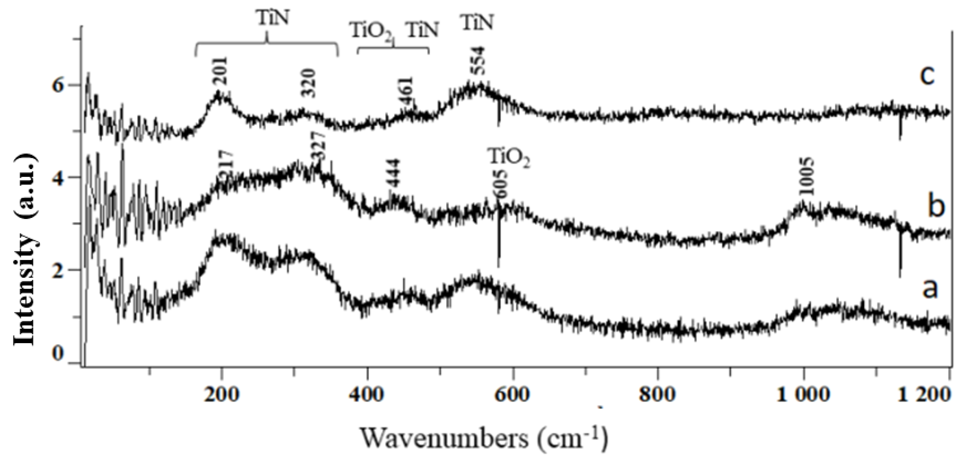
3.2.2. Raman Investigations

Raman spectroscopy measurements carried out on Mo–Ti bilayer films processed at 600 and 800 °C confirm the XRD results (Figure 5).
The Raman signal corresponding to the Mo–Ti bilayer film processed at 600 °C for 1 h 30 min is well structured and typical of the first-order Raman scattering of TiN compound (Figure 5a). TiN crystallizes in the high symmetry of B1-structured materials of NaCl type, which does not display any first-order Raman scattering due to the Oh symmetry. However, because of the presence of point defects such as metal and nitrogen vacancies, the crystal symmetry is broken [26,27]. On Figure 5a, the Raman signal consists of two main regions of intense features, in the acoustic frequency region ranging between 200 and 350 cm−1 and in the optical frequency region ranging between 500 and 600 cm−1. The scattering identified in the acoustic range is assigned to vibrations of heavy Ti ions and the one in the optic range to vibrations of lighter N ions. Since the Raman features are rather broad, especially those located in the acoustic frequency range, TiN is amorphous or consists of small sized-crystallites. Ti oxides are also identified on Figure 5a. The broad band located around 450 cm−1 could be a convolution of the vibrational modes of TiN at 464 cm−1 and TiO2 at 446 cm−1 whereas the shoulder identified at the high wave number side of TiN band, located at about 550 cm−1 is due to the presence of TiO2. TiO2 in the rutile phase usually shows the most intense Eg and A1g modes at 446 and 612 cm−1 [15].
Longer treatment durations result in a strong decrease of the intensity of the Raman signal corresponding to TiN and especially the intensity of the transverse acoustic (TA) and optical (TO) modes at 200 and 550 cm−1, respectively (Figure 5b). This phenomenon is assigned to Raman measurements since spectra are obtained from the light scattered normal to the sample surface, which promotes the longitudinal modes. So, only the longitudinal acoustic mode at about 320 cm−1 is still identified as well as the Raman signals corresponding to TiO2. Such a strong decrease of the TiN signal has also been observed in XRD patterns and may be assigned to the etching effect of hydrogen species. Poorly crystallized compounds should be more sensitive to this effect.
It can also be noticed that both Raman spectra (a) and (b) in Figure 5 exhibit features at high wave numbers located around 1050 cm−1. The presence of such a broad band is quite surprising. Its shape is similar to the three dome-like bands, usually identified at wave numbers of about 737, 848 and 947 cm−1 which correspond to Mo oxides present in Mo films [13]. Interestingly, Stampfl et al. in [28], highlighted the interaction of MoO3 with various metal oxides used for the preparation of supported Mo catalysts. Results show that the characteristic peaks in metal-oxide stretching region at 816 and 992 cm−1 disappeared. New peaks are identified in the wave numbers region ranging from 800 to 1100 cm−1, depending on the metal oxide support. To our knowledge, this is the only work reporting such phenomenon. In the light of this work, we can conclude that because of Ti–Mo interactions, mixed Ti–Mo oxides could be identified by a broad band, at wave numbers higher than the characteristic vibrational modes of Mo oxides. Further experiments are needed to confirm such a result.
The characteristic Raman scattering bands of TiN are well identified in the spectrum (c) in Figure 5, recorded on Mo–Ti bilayer films processed at 800 °C for 3 h. The result is quite similar to the one obtained for Ti films processed under same experimental conditions [15]. TiN is well crystallized. Moreover, the second order broad bands at 825 and 1128 cm−1 are also identified. The presence of TiO2 is less pronounced than in films processed at 600 °C. Except TiN and TiO2, no other features are identified on spectrum (c). On the assumption that the broad band located around 1050 cm−1 corresponds to mixed Ti–Mo oxides, the result shows that they are fully reduced by hydrogen species such as NHx and H produced in the plasma. It is worth noting that, although MoSi2 displays two active vibrational modes A1g and Eg at 325, and 440 cm−1, respectively [24], the spectrum (c) does not exhibit any features. They are in the same range of wave numbers as the characteristic Raman bands of TiN, which are intense after processing for 3 h, while on the other hand the surface layer of TiN should be sufficient to block any Raman emissions from MoSi2. In what follows, the nitrogen diffusion into Mo–Ti bilayer films as well as the interdiffusion of Ti, Mo, and Si elements across Ti–Mo and Mo–Ti interfaces of Mo–Ti bilayer films heated at 400, 600 and 800 °C and exposed to (Ar-N2-H2) plasma for 1 h are investigated by SIMS experiments.

3.3. Diffusion at Ti Surface and Ti–Mo and Mo–Si Interfaces

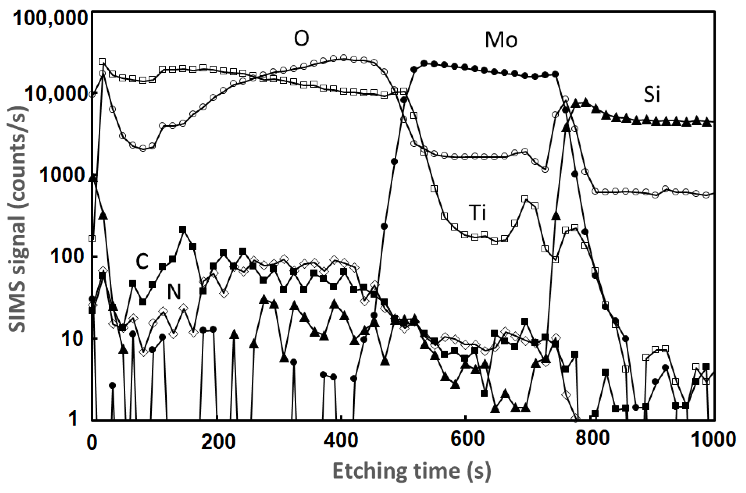
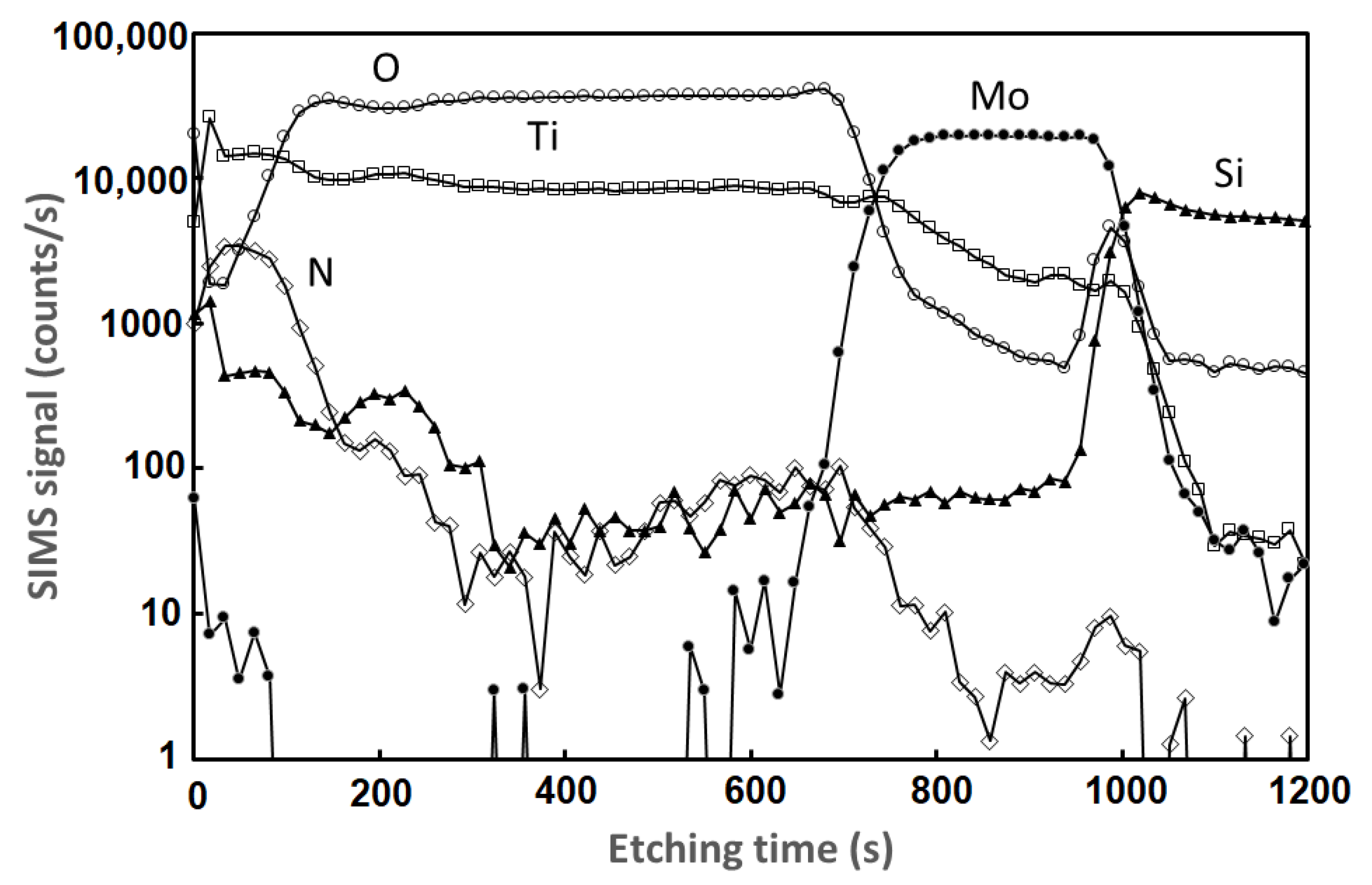
3.3.1. Mo–Ti Bilayer Films Processed at 400 °C

The N signal profile in Figure 6 clearly shows that nitrogen starts to diffuse into the surface layers of the Ti film at low temperature.
Nitrogen is incorporated in the surface region up to a depth of about one quarter of the thickness of Ti film. As for the untreated Mo–Ti bilayer films, both Mo–Ti and Si–Mo interfaces are well identified. The various elements contained in Mo–Ti bilayer films processed at 400 °C do not diffuse through both interfaces. The oxygen SIMS signal intensity remains high in the whole Ti film, especially in the vicinity of the surface and Ti–Mo interface.

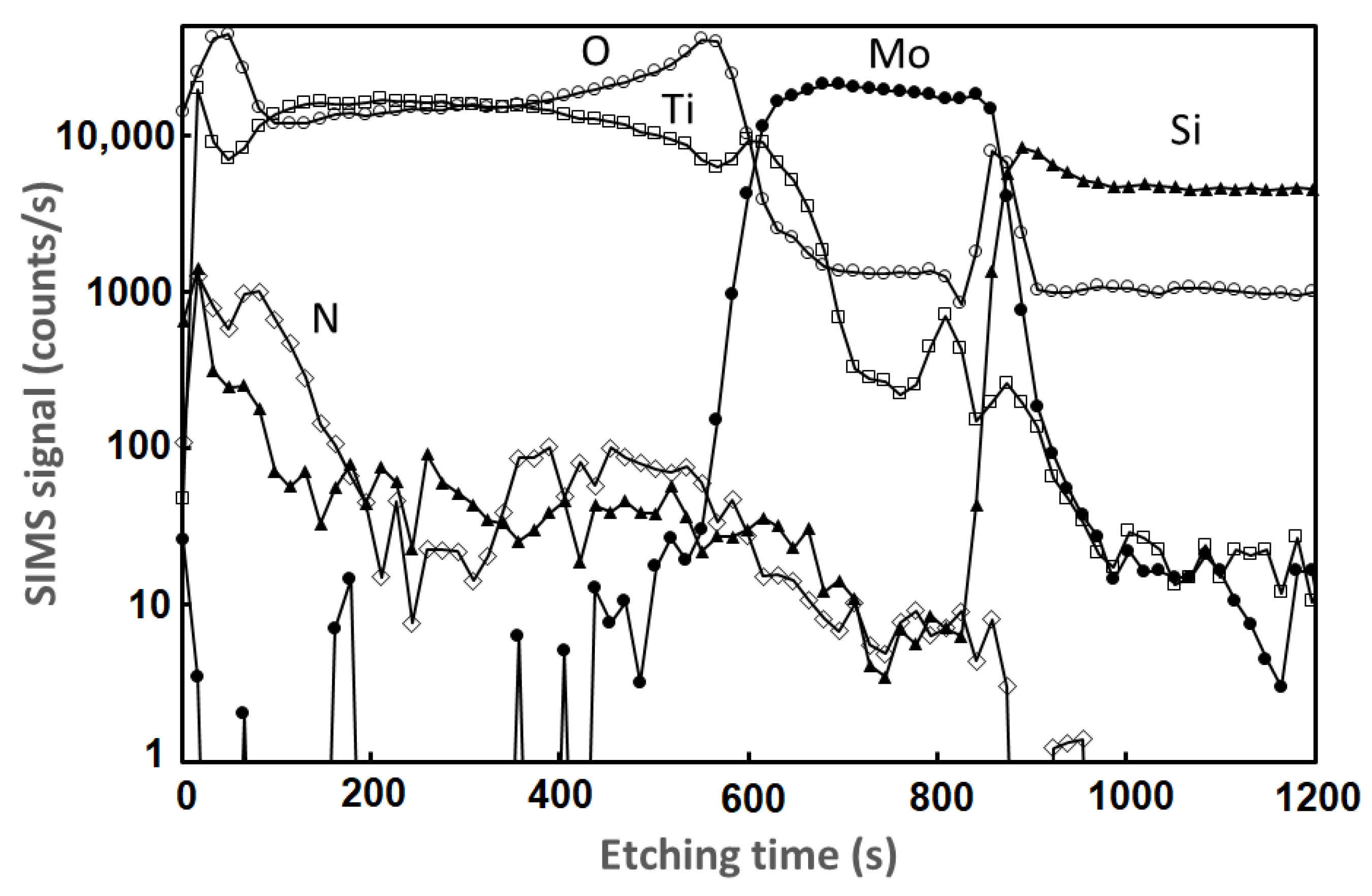
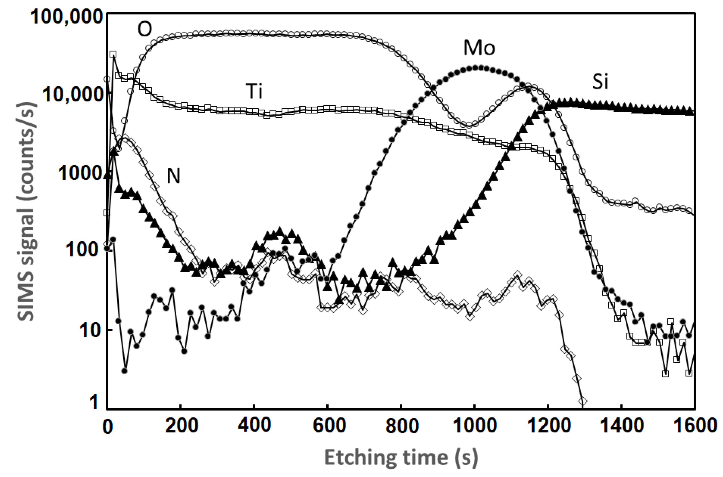
3.3.2. Mo–Ti Bilayer Films Processed at 600 and 800 °C

The diffusion of nitrogen into the film greatly increases with increasing temperature. The amount of nitrogen incorporated into the surface region is greatly enhanced in Mo–Ti bilayer films processed at 600 and 800 °C (Figure 7 and Figure 8). Interestingly, a strong depletion of oxygen SIMS intensity is observed in the first surface layers. NHx and H species produced in the plasma reduce the surface oxides, which allows the transfer of nitrogen into the Ti film to be improved. Such an effect is correlated to the decrease of TiO2 amount in Mo–Ti bilayer films processed at 800 °C.
Two diffusion modes are identified by the change of the slope of nitrogen signal in the surface region of Mo–Ti bilayer films processed at 600 °C. It can be also noticed that Si starts to diffuse into the Mo film in the opposite direction with a roughly constant amount through the Mo film. This result is correlated with the formation of Mo silicides before they crystallize at higher temperature. The amount of nitrogen incorporated in the surface region of the Mo–Ti bilayer film processed at 600 and 800 °C are rather similar, but nitrogen seems to penetrate deeper into the Mo–Ti bilayer with increasing temperature.
The change of slope in the diffusion profile of nitrogen also seen at 800 °C, could correspond to additional interfaces in Mo–Ti bilayer films processed at high temperature. This result will be clarified in next sections. It is worth noting that an outstanding change in the form of the Mo signal is well identified at 800 °C. The Mo–Ti interface is broader which indicates a strong interdiffusion of Mo and Ti. In the same way, Si diffuses through the whole Mo layer. This result is correlated to the crystallization of MoSi2 compounds at 800 °C.
The interdiffusion of Ti, Mo, and Si across Si–Mo and Mo–Ti interfaces is also well identified in Figure 9, which displays the elemental composition of Mo–Ti bilayer films processed at 800 °C for 1 h 30 min, along a line scan carried out across the interfaces by EDS.
The distribution of concentration of Ti from the surface up to the Mo film is identified as strongly uneven, which seems related to the formation of a heterogeneous structure in Ti films. The Ti content is constant in the first surface layers up to a depth of about 40 nm, then decreases from the surface to 50 at.% at a depth of about 130 nm, where it remains constant up to the Ti–Mo interface, and then strongly decreases up to about 10 at.% in the Mo film. In the same way, Si strongly diffuses in the opposite direction through the whole Mo layer. Its content reaches a value of about 10 at.% at the Ti–Mo interface, then it slowly decreases up to the surface of the bilayer film. The distribution of Mo concentration is well correlated to the corresponding Mo SIMS diffusion profile, i.e. Mo diffuses both into Ti film and Si wafer. In contrast with Si content, the Mo content is trifling in surface layers. The distribution of Cr and Cu concentration have not been reported in the figure. The presence of Cr and Cu are due to the polar piece, sample holder and grid on which the sample is deposited for TEM measurements.

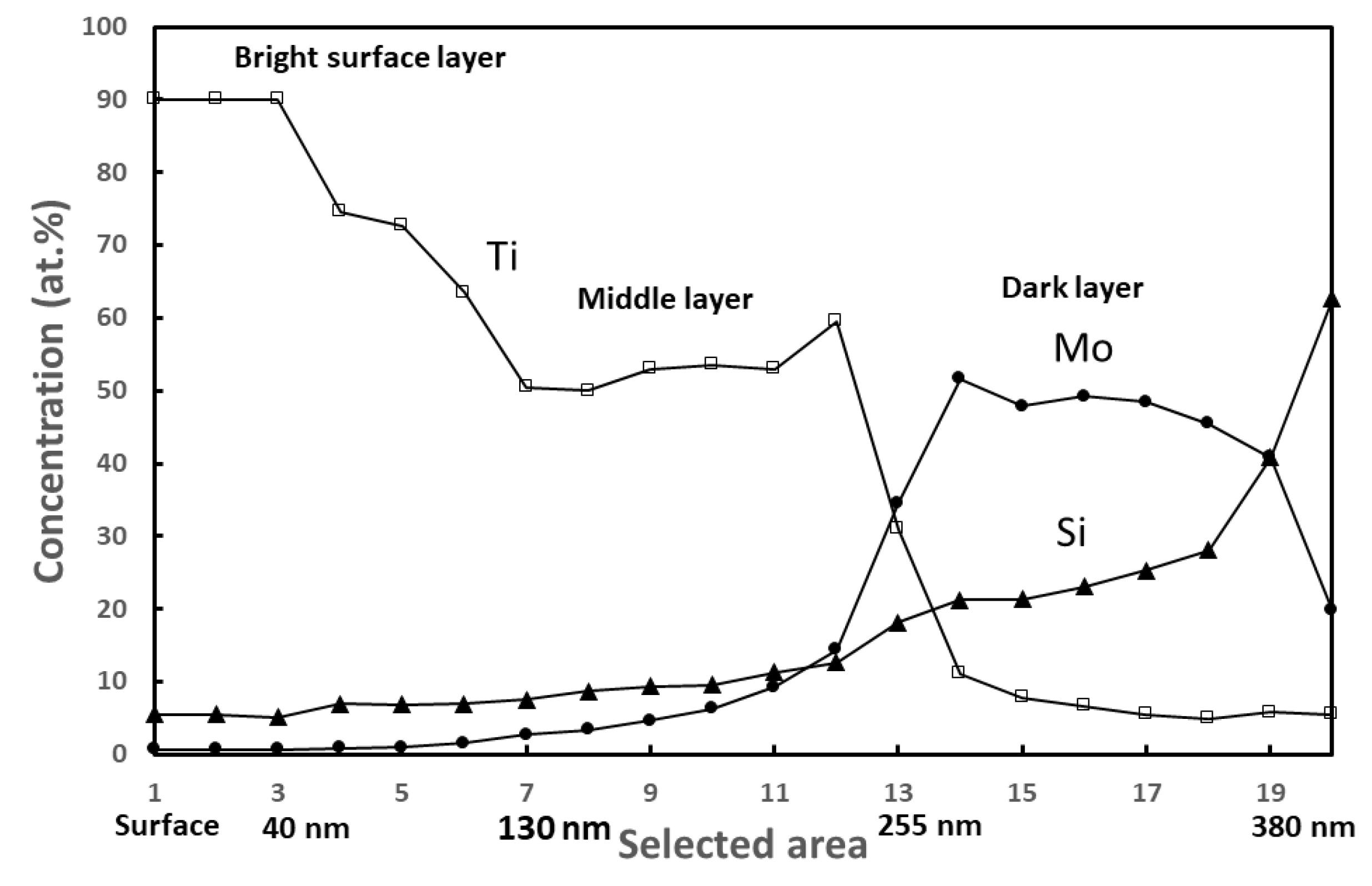
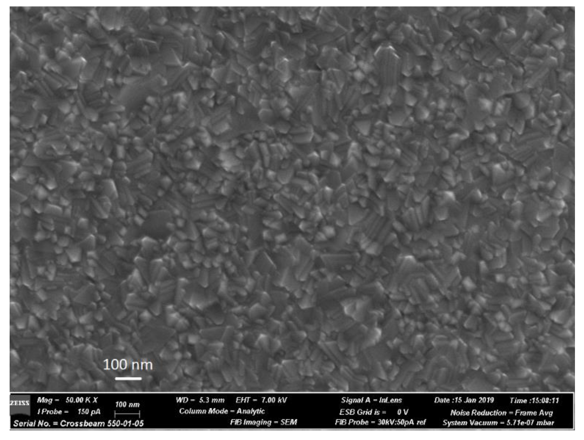
3.4. Microstructural Properties of Mo–Ti Bilayer Processed at 800 °C

The morphology and the microstructures of Mo–Ti bilayer films are investigated by means of TEM, SAED, and SEM. The cross-sectional bright-field electron micrograph (a) of the Mo–Ti bilayer film coated on Si substrate after processing at 800 °C for 1 h 30 min, is displayed in Figure 10.
Three distinct layers of nearly equal thickness of about 150 nm are clearly seen. The thickness of the bilayer film is found to vary from 400 to 480 nm. The layers exhibit three different grey tints which vary from dark to light from the Mo–Si interface up to the surface. Since Mo is the heaviest element, it absorbs more the electron beam than other elements, so the variation from dark to light grey reflects the gradient of concentration of Mo through the Mo–Ti bilayer film. The first layer located in the vicinity of the surface is rough on a micrometer scale compared with the other two layers. It is formed of two sub-layers, one consisting entirely of many square-shaped crystals ranging from about 20 to 70 nm wide, whereas the second one consists of rather round crystals of sizes not larger than 100 nm (Figure 10b). The morphology of the first layer reflects the uneven Ti distribution shown in Figure 9. The Ti content is constant in the layer consisting of square shaped crystals up to the second sub-layer and then decreases. The SAED pattern (c) in Figure 10 has been taken on the crystal (d) in Figure 10. It is identified as the TiN phase of cubic structure orientated along its [110] zone axis. TiN crystals are usually orientated along their [110] crystallographic direction, so they tend to display a flattened morphology with the [110] direction perpendicular to the flat surface. The SAED pattern (c) also shows that they are oriented along their [−220] crystallographic direction in the growth direction of the film. The SAED pattern (a) in Figure 11 has been taken on the first layer, it is identified as a mixture of TiN phase of cubic structure and MoSi2 of hexagonal structure.
So, in addition to TiN, MoSi2 crystallizes in the layer consisting of round crystals where a gradual decrease of Ti content has been identified by EDS. The second layer located in the middle of the Mo–Ti bilayer film also consists of round crystals of hexagonal MoSi2. The content of Ti through this layer is also constant, because the layer probably mainly consists of Mo–Ti alloys. In contrast, the darker layer located in the vicinity of Si wafer mainly consists of pure Mo. The columnar structure of Mo is displayed on the high resolution TEM (HRTEM) image (b) in Figure 11, and its polycrystalline structure is clearly identified on the SAED pattern (c). The interfaces between the various layers are clearly identified in Figure 10a,b and Figure 11b. They are brighter than the layers and seem to consist of a mixture of amorphous and crystallized structures of nanometric size which gives them a rough aspect on a nanometric scale (HRTEM images Figure 10b and Figure 11b). Since Si is more transparent in the electron beam than TiN and MoSi2, the interfaces are expected to mainly consist of Si, which has diffused through Mo–Ti bilayer films processed at 800 °C. The morphology of Mo–Ti bilayer films processed at 800 °C for 1 h 30 min consists of strongly faceted grains of nanometric size with triangular morphology, uniformly distributed over the surface of samples (Figure 12).

4. Discussion

The results reported in this paper highlight the strong ability of the components of Mo–Ti bilayer films coated on Si wafer to diffuse across various interfaces. The diffusion of nitrogen into the surface layers of the material heated at 600 and 800 °C and exposed to (Ar-31%N2-6%H 2) plasma as well as the diffusion of Si and Mo across Si–Mo and Mo–Ti interfaces give rise to the formation and crystallization of TiN and MoSi2, which are both thermodynamically and kinetically controlled.
Ti diffused into the whole Mo film during the synthesis of Mo–Ti bilayer by evaporation, which results in the formation of binary Ti–Mo alloys. Among them, Ti0.9Mo0.1 crystallizes. At the end of the evaporating process, the Mo–Ti bilayer consists of Mo, Ti–Mo alloys, and Ti in the form of TiO2 of amorphous structure. Ti reacted with oxygen which was incorporated during the evaporating process. It is well known that Ti strongly reacts with oxygen; the enthalpy of formation of TiO2 is equal to −944 kJ·mol−1 at room temperature [29], compared with those of MoO2 and MoO3 which are equal to −598.94 kJ·mol−1 and −745.05 kJ·mol−1, respectively [30]. TiO2 crystallizes in Mo–Ti bilayer films processed in expanding plasma at 600 and 800 °C. The anatase phase is the predominant form at 600 °C, and it turns into the rutile phase at higher temperatures. Owing to the reducing effect of gaseous species produced in (Ar-N2-H2) plasma and especially NHx and H, oxide species amount tends to decrease with increasing treatment duration. Hydrogen species play an important role in the reduction of remaining oxides. They also prevent the formation of oxides, which come from oxygen or water adsorbed on the wall of the reactor and added to the plasma. Oxides contained in the surface layers form a barrier of diffusion which prevents nitrogen diffusion. The enthalpy of the formation of TiN is very low compared with the one of TiO2. The value is equal to −338 kJ·mol−1 [29]. So, hydrogen species allow the barrier of the diffusion of oxides to be reduced and promote the formation of TiN. The oxygen content is trifling in the first layers of Mo–Ti bilayer films, which only consist of TiN crystals. The occurrence of exothermic chemical reactions between the plasma and the surface of the metal has been evidenced during the formation of Mo nitrides [13]. These properties make the plasma expanding process very different from sputtering or implantation processes where the impinging ions of high energy plays the main role. In the same way as Ti films, nitrogen starts to diffuse into the surface layers of the metal, at a low temperature of about 400 °C, from NHx species produced in the plasma which react at the metal surface. TiN starts to crystallize at 600 °C in Mo–Ti bilayer films in contrast with Ti films which are fully transformed into TiSi2 after processing at 600 °C for 30 min. TiSi2 prevents TiN from crystallizing at temperatures lower than 800 °C [15]. The TiN layer consists of small crystals of nanometric size oriented along their [−220] crystallographic direction in the growth direction of the film. In the opposite direction of nitrogen diffusion, silicon starts to diffuse from the Mo–Si interface through to the Mo layer at 600 °C. At 800 °C, Si and Mo diffuse up to the surface, MoSi2 crystallizes in hexagonal structure in the vicinity of TiN crystals, and then continuously transformed into MoSi2 of tetragonal structure for longer treatment durations. It is worth noting that crystals of MoSi2 also exhibit nanometric dimensions in the vicinity of TiN crystals after plasma processing for 1 h 30 min. The enthalpy of formation of MoSi2 at 25 °C, equal to −137 kJ·mol−1 [31], is slightly lower than the one of TiSi2. Owing to the strong interdiffusion of various elements across the interfaces and the formation of TiN and MoSi2 crystallized phases, the Mo–Ti bilayer films heated at 800 °C and processed for 1 h 30 min exhibits very heterogeneous structures. Three layers of nearly equal thickness with clear interfaces have been identified, as well as additional interfaces in the surface layers. The gradual conversion of TiSi2 into TiN phase has been successfully evidenced in Ti films exposed to (Ar-N2-H2) expanding plasma and has been related to the reaction between TiSi2 and nitrogen on TiSi2 surface and grain boundaries. Si released during the reaction moves towards Si substrate, where it epitaxially crystallizes [14]. So, further investigations on the development of Mo–Ti bilayer films during plasma processing would improve the understanding of the structural properties of TiN and MoSi2 and the reaction at interfaces. The influence of gaseous species produced in (Ar-N2-H2) plasma on the formation of nitrides would be studied in the case of Mo–Ti bilayer films. A reduction-nitridation process has been evidenced during the nitriding process of Mo thin films with the formation of the high temperature Mo2N phase [13]. A better understanding of the growth process of these compounds could be interesting, since TiSi2 and TiN exhibit low resistivity equal to 15 and 30 μΩ·cm, respectively whereas MoSi2 of hexagonal structure is a narrow gap semiconductor with a band gap of 0.035 eV [32]. This value has been mainly investigated by density functional theory [33,34,35] and also by valence band X-ray photoelectron spectroscopy [35].

5. Conclusions

An expanding plasma process carried out on Mo–Ti bilayer films heated at 800 °C resulted in the formation of a very heterogeneous structure arising from the diffusion of nitrogen into surface layers on one hand, and strong interdiffusions of Ti, Mo, and Si through interfaces on the other hand. Nitrogen starts to diffuse at 400 °C, whereas Si and Mo start to diffuse at 600 °C. TiN crystallites of nanometric size are identified at 600 °C and MoSi2 crystallites of nanometric size form at 800 °C in the surface layers. Further investigations carried out on Mo–Ti bilayer films processed for longer treatment durations could improve the comprehension of mechanisms involved in the growth of both nitrides and silicides. Moreover, since TiN is a good conductor and MoSi2, a good semiconductor, electrical conductivity measurements will be performed.

Author Contributions

Conceptualization, I.J. and J.L.J.; Methodology, I.J., A.B.; Validation, A.B., J.L.J., I.J.; Formal Analysis, I.J.; Investigation, R.M., J.C., P.C., D.M., A.B., A.P.; Data Curation, I.J. and R.M.; Writing-Original Draft Preparation, I.J.

Funding

This research received no external funding.

Acknowledgments

We thank Therèse Merle-Méjean for helpful discussions. Région Limousin is acknowledged for the support of work on the surface reactivity.

Conflicts of Interest

The authors declare no conflict of interest.

References

  1. Oyama, S.T. Introduction to the chemistry of transition metal carbides and nitrides. In The Chemistry of Transition Carbides and Nitrides, 1st ed.; Oyama, S.T., Ed.; Springer: Dordrecht, The Netherlands, 1996; pp. 2–10. [Google Scholar]
  2. Jauberteau, I.; Bessaudou, A.; Mayet, R.; Cornette, J.; Jauberteau, J.L.; Carles, P.; Merle-Méjean, T. Molybdenum nitride films: Crystal structures, synthesis, mechanical, electrical and some other properties. Coatings 2015, 5, 656–687. [Google Scholar] [CrossRef]
  3. Ponon, N.K.; Appleby, D.J.; Arac, E.; King, P.J.; Ganti, S.; Kwa, K.S.K.; O’Neill, A. Effect of deposition conditions and postdeposition anneal on reactively sputtered titanium nitride films. Thin Solid Films 2015, 578, 31–37. [Google Scholar] [CrossRef]
  4. Bhaskaran, M.; Sriram, S.; Short, K.T.; Mitchell, D.R.G.; Holland, A.S.; Reeves, G.K. Characterization of C54 titanium silicide thin films by spectroscopy, microscopy and diffraction. J. Phys. D Appl. Phys. 2007, 40, 5213–5219. [Google Scholar] [CrossRef]
  5. Yanisagawa, S.; Fukuyama, T. Preparation of molybdenum silicide films by reactive sputtering. J. Electrochem. Soc. 1980, 127, 1120–1124. [Google Scholar] [CrossRef]
  6. Lima, L.P.B.; Diniz, J.A.; Doi, I.; Fo, J.G. Titanium nitride as electrode for MOS technology and Schottky diode: Alternative extraction method of titanium nitride work function. Microelectron. Eng. 2012, 92, 86–90. [Google Scholar] [CrossRef]
  7. Wang, L.-L.; Peng, W.; Jiang, Y.-L.; Li, B.-Z. Effective Schottky barrier height lowering by TiN capping layer for TiSix/Si power diode. IEEE Electron Device Lett. 2015, 36, 597–599. [Google Scholar] [CrossRef]
  8. Pshyk, A.V.; Kravchenko, Y.; Coy, E.; Kempinski, M.; Iatsunskyi, I.; Zaleski, K.; Pogrebnjak, A.D.; Jurga, S. Microstructure, phase composition and mechanical properties of novel nanocomposite (TiAlSiY)N and nano-scale (TiAlSiY)N/MoN multifunctional heterostructures. Surf. Coat. Technol. 2018, 350, 376–390. [Google Scholar] [CrossRef]
  9. Ting, Y.-J.; Lian, K.; Kherani, N. Fabrication of titanium nitride and molybdenum nitride for supercapacitor electrode application. ECS Trans. 2011, 35, 133–139. [Google Scholar] [CrossRef]
  10. Xie, Y.; Tian, F. Capacitive performance of molybdenum nitride/titanium nitride nanotube array for supercapacitor. Mater. Sci. Eng. B 2017, 215, 64–70. [Google Scholar] [CrossRef]
  11. Blösch, P.; Güttler, D.; Chirila, A.; Tiwari, A.N. Optimization of Ti/TiN/Mo back contact properties of Cu (In,Ga)Se2 solar cells on polyimide foils. Thin Solid Films 2011, 519, 7453–7457. [Google Scholar] [CrossRef]
  12. Li, W.; Yan, X.; Aberle, A.G.; Venkataraj, S. Effect of a TiN alkali diffusion barrier layer on the physical properties of Mo back electrodes for CIGS solar cell applications. Curr. Appl. Phys. 2017, 17, 1747–1753. [Google Scholar] [CrossRef]
  13. Jauberteau, I.; Mayet, R.; Cornette, J.; Bessaudou, A.; Carles, P.; Jauberteau, J.L.; Merle-Méjean, T. A reduction-nitridation process of molybdenum films in expanding microwave plasma: Crystal structure of molybdenum nitrides. Surf. Coat. Technol. 2015, 270, 77–85. [Google Scholar] [CrossRef]
  14. Jauberteau, I.; Carles, P.; Mayet, R.; Cornette, J.; Bessaudou, A.; Jauberteau, J.L. Competing growth of titanium nitrides and silicides in Ti films processed in expanding microwave plasma: Morphology and microstructural properties. AIP Adv. 2018, 8, 095105. [Google Scholar] [CrossRef]
  15. Jauberteau, I.; Mayet, R.; Cornette, J.; Mangin, D.; Bessaudou, A.; Carles, P.; Jauberteau, J.L.; Passelergue, A. Silicides and nitrides formation in Ti films coated on Si and exposed to (Ar-N2-H2) expanding plasma. Coatings 2017, 7, 23. [Google Scholar] [CrossRef]
  16. Xin, C.; Liu, W.; Li, N.; Yan, J.; Shi, S. Metallization of Al2O3 ceramic by magnetron sputtering Ti/Mo bilayer thin films for robust brazing to Kovar alloy. Ceram. Int. 2016, 42, 9599–9604. [Google Scholar] [CrossRef]
  17. Ruzic, J.; Emura, S.; Ji, X.; Watanabe, I. Mo segregation and distribution in Ti-Mo alloys investigated using nanoindentation. Mater. Sci. Eng. A 2018, 718, 48–55. [Google Scholar] [CrossRef]
  18. Fan, J.; Lu, M.; Cheng, H.; Tian, J.; Huang, B. Effect of alloying elements Ti, Zr, on the property and microstructure of molybdenum. Int. J. Refract. Hard Mater. 2009, 27, 78–82. [Google Scholar] [CrossRef]
  19. Kislitin, S.B.; Potekaev, A.I.; Uglov, V.V.; Klopotov, A.A.; Klopotov, V.D.; Ivanov, Y.F.; Parpiev, A.T. Steel suface TiCrN, TiMoN coatings structural phase state change features after low-energy alpha particles irradiation. IOP Conf. Ser. Mater. Sci. Eng. 2018, 289, 012010. [Google Scholar] [CrossRef]
  20. Oliveira, N.T.C.; Aleixo, G.; Caram, R.; Guastaldi, A.C. Development of Ti-Mo alloys for biomedical applications: Microstructures and electrochemical characterization. Mater. Sci. Eng. A 2007, 452, 727–731. [Google Scholar] [CrossRef]
  21. Simka, W.; Krzakala, A.; Korotin, D.M.; Zhidkov, I.S.; Kurmaev, E.Z.; Cholakh, S.O.; Kuna, K.; Dercz, G.; Michalska, J.; Suchanek, K.; et al. Modification of a Ti–Mo alloy surface via plasma electrolytic oxidation in a solution containing calcium and phosphorus. Electrochem. Acta 2013, 96, 180–190. [Google Scholar] [CrossRef]
  22. Zhang, W.-D.; Liu, Y.; Wu, H.; Song, M.; Zhang, X.-D.; Lan, X.-D.; Yao, T.-H. Elastic modulus of phases in Ti–Mo alloys. Mater. Charact. 2015, 106, 302–309. [Google Scholar] [CrossRef]
  23. Gu, M.; Bai, S.; Xia, X.; Huang, X.; Li, X.; Shi, X.; Chen, L. Study of the high temperature interfacial stability of Ti/Mo/Yb0.3Co4Sb12 thermoelectric joints. Appl. Sci. 2017, 7, 952. [Google Scholar] [CrossRef]
  24. Cai, M.; Allred, D.D. Raman spectroscopic study of the formation of t-MoSi2 from Mo/Si multilayers. J. Vac. Sci. Technol. A 1994, 12, 1535–1541. [Google Scholar] [CrossRef]
  25. Chi, E.; Shim, J.; Kwak, J.; Baik, H. Silicide formation by solid-state diffusion in Mo/Si multilayer thin films. J. Mater. Sci. 1996, 31, 3567–3572. [Google Scholar] [CrossRef]
  26. Constable, C.P.; Yarwood, J.; Münz, W.D. Raman microscopic studies of PVD hard coatings. Surf. Coat. Technol. 1999, 116, 155–159. [Google Scholar] [CrossRef]
  27. Stoehr, M.; Shin, C.-S.; Petrov, I.; Greene, J.E. Raman scattering from TiNx(0.67 < x < 1.00) single crystals grown on MgO (001). J. Appl. Phys. 2011, 110, 083503. [Google Scholar] [CrossRef]
  28. Stampfl, S.R.; Chen, Y.; Dumesic, J.A.; Niu, C.; Hill, C.G., Jr. Interactions of molybdenum oxide with various oxide supports. Calcination of mechanical mixtures. J. Catal. 1987, 105, 445–454. [Google Scholar] [CrossRef]
  29. Barhai, P.K.; Kumari, N.; Banerjee, I.; Pabi, S.K.; Mahapatra, S.K. Study of the effect of plasma current density on the formation of titanium nitride ant titanium oxynitride thin films prepared by reactive DC magnetron sputtering. Vacuum 2010, 84, 896–901. [Google Scholar] [CrossRef]
  30. Birtill, J.J.; Dickens, P.G. Thermochemistry of hydrogen molybdenum bronze phases HxMoO3. J. Solid State Chem. 1979, 29, 367–372. [Google Scholar] [CrossRef]
  31. O’Hare, P.A.G. Thermodynamic properties of silicides. III. Specific energy of combustion in fluorine of a hyperstoichiometric disilicide. The standard molar enthalpy of formation ΔfH°m of MoSi2.067±0.002 at the temperature 298.15 K. J. Chem. Thermodyn. 1993, 25, 1333–1343. [Google Scholar] [CrossRef]
  32. Ohishi, Y.; Kurosaki, K.; Suzuki, T.; Muta, H.; Yamanaka, S.; Uchida, N.; Tada, T.; Kanayama, T. Synthesis of silicon and molybdenum-silicide nanocrystal composite films having low thermal conductivity. Thin Solid Films 2013, 534, 238–241. [Google Scholar] [CrossRef]
  33. Shugani, M.; Aynyas, M.; Sanyal, S.P.; Rajagopalan, M. Electronic properties of MoSi2. Indian J. Pure Appl. Phys. 2013, 51, 634–637. (In English) [Google Scholar]
  34. Mattheiss, L.F. Calculated structural properties of CrSi2, MoSi2 and WSi2. Phys. Rev. B 1992, 45, 3252–3259. [Google Scholar] [CrossRef]
  35. Pankhurst, D.A.; Yuan, Z.; Nguyen-Manh, D.; Abel, M.-L.; Shao, G.; Watts, J.F.; Pettifor, D.G.; Tsakiropoulos, P. Electronic structure and bonding in MoSi3, Mo5Si3 and Mo(Si,Al)2 alloys investigated by X-ray photoelectron spectroscopy and density-functional theory. Phys. Rev. B 2005, 71, 075114. [Google Scholar] [CrossRef]
Figure 1. Experimental set-up [15].
Coatings 09 00096 g001
Figure 2. X-ray diffraction pattern of untreated Mo–Ti, 250–250 nm, thick bilayer film.
Coatings 09 00096 g002
Figure 3. SIMS depth profiles of as-deposited Mo–Ti bilayer films.
Coatings 09 00096 g003
Figure 4. X-ray diffraction patterns of Mo–Ti bilayer films heated at 600 °C and exposed to (Ar-31%N2-6%H2) for 1 h 30 min (a), 3 h (b), heated at 800 °C and exposed to (Ar-31%N2-6%H2) plasma for 1 h 30 min (c) and 3 h (d).
Coatings 09 00096 g004
Figure 5. Raman scattering spectra of Mo–Ti bilayer films heated at 600 °C and exposed to (Ar-31%N2-6%H2) plasma for 1 h 30 min (a) and 3 h (b), heated at 800 °C and exposed to (Ar-31%N2-6%H2) plasma for 3 h (c).
Coatings 09 00096 g005
Figure 6. SIMS depth profiles of Mo–Ti bilayer film heated at 400 °C and exposed to (Ar-31%N2-6%H2) plasma for 1 h.
Coatings 09 00096 g006
Figure 7. SIMS depth profiles of Mo–Ti bilayer film heated at 600 °C and exposed to (Ar-31%N2-6%H2) plasma for 1 h.
Coatings 09 00096 g007
Figure 8. SIMS depth profiles of Mo–Ti bilayer films heated at 800 °C and exposed to (Ar-31%N2-6%H2) plasma for 1 h.
Coatings 09 00096 g008
Figure 9. EDS Line scan results providing the concentration of Ti, Mo and Si (at.%) in Mo–Ti bilayer films heated at 800 °C and exposed to (Ar-31%N2-6%H2) plasma for 1 h 30 min.
Coatings 09 00096 g009
Figure 10. Cross-sectional transmission electron micrograph of the Mo–Ti bilayer film heated at 800 °C and exposed to (Ar-31%N2-6%H2) plasma for 1 h 30 min (a), (b). SAED pattern of TiN crystallites (c) and high-resolution TEM (HRTEM) image of TiN crystallites (d), (e). ll.
Coatings 09 00096 g010
Figure 11. SAED pattern of surface layer and dark layer of the Mo–Ti bilayer film heated at 800 °C and exposed to (Ar-31%N2-6%H2) plasma for 1.5 h (a,c), respectively. HRTEM image of the interface between middle layer and dark layer (b).
Coatings 09 00096 g011
Figure 12. SEM image of the surface of Mo–Ti bilayer films heated at 800 °C and exposed to (Ar-31%N2-6%H2) plasma for 1 h 30 min.
Coatings 09 00096 g012

