Article

Characterization of Nitrogen-Doped TiO2 Films Prepared by Arc Ion Plating without Substrate Heating in Various N2/O2 Gas Mixture Ratios

1
System Manufacturing Center, National Chung-Shan Institute of Science and Technology, New Taipei City 237209, Taiwan
2
Center for Astronomical Physics and Engineering, Department of Optics and Photonics, National Central University, Taoyuan City 320317, Taiwan
3
Department of Physics, Fu Jen Catholic University, New Taipei City 242062, Taiwan
4
Department of Electronic Engineering, Ming Chi University of Technology, New Taipei City 24301, Taiwan
5
Department of Engineering and Technology, School of Computing and Engineering, University of Huddersfield, Queensgate, Huddersfield HD1 3DH, UK
6
Graduate Institute of Applied Science and Engineering, Fu Jen Catholic University, New Taipei City 242062, Taiwan
*
Authors to whom correspondence should be addressed.
Coatings 2023, 13(3), 654; https://doi.org/10.3390/coatings13030654
Submission received: 28 February 2023 / Revised: 17 March 2023 / Accepted: 18 March 2023 / Published: 20 March 2023
(This article belongs to the Special Issue Design, Manufacturing and Measurement of Optical Film Coatings II)

Abstract

:
Nitrogen-doped TiO2 films exhibit good photocatalytic ability in the visible (VIS) light region. This study reports the fabrication of these films using arc ion plating (AIP) in different ratios of nitrogen partial pressure (PN2) to oxygen partial pressure (PO2) without substrate heating and/or applied bias. This approach allows a significant broadening of the range of possible substrates to be used. X-ray diffraction (XRD) patterns indicate that these films deposited at room temperature are amorphous, and surface electron microscope (SEM) and atomic force microscope (AFM) images show that they have rough surfaces. Their transmittance and optical properties are measured with a spectrometer and ellipsometer, respectively. In addition, the bandgap energies of these amorphous films are derived by the ellipsometer from the Tauc–Lorentz (TL) model. The results indicate that the N-doped TiO2 film with a PN2/PO2 ratio of 1/4 attains the narrowest bandgap and the highest absorbance in the visible region. It can be attributed to the prominent Ti–N peaks observed in the sample’s Ti and N X-ray photoelectron spectroscopy (XPS) spectra. In addition, verified with the methylene blue (MB) test, this sample exhibits the best photocatalytic performance for its narrowest energy gap.

1. Introduction

Photocatalysis refers to a photo-activated process where pairs of chemical reactions occur to decompose organic molecules. It is widely used in various applications, including air and water purification, self-cleaning, deodorizing, sterilization, and sustainable regeneration [1,2,3,4]. The most commonly used photocatalysts are semiconductors such as ZnO, WO3, SnO2, and TiO2 [5,6,7,8,9]. The photocatalytic performance of a semiconductor depends on its electronic band structure and bandgap energy, with, in general, a narrower gap giving a higher catalytic capability [10]. Among these materials, TiO2 has been extensively investigated due to its low cost, photostability, redox efficiency, nontoxicity, and availability [11]. Through strong redox processes, TiO2 is able to attain photocatalytic decomposition of organic pollutants in water and air [12]. TiO2 has three stable crystal phases: tetragonal anatase, rutile, and orthorhombic brookite. The anatase phase possesses the best photocatalytic efficiency because its surface area is larger than the rutile one, resulting in larger reaction areas for surface water molecules [13]. With a bandgap of around 3.2 eV for anatase TiO2, an ultraviolet (UV) light at about 385 nm releases the electrons on its surface to form positively charged electron holes. Then hydroxyl groups (-OH) released by nearby water molecules are oxidized and become very active hydroxyl radicals. As an organic molecule comes across these radicals, its electrons will be captured, leading to the breakdown of its bonds and subsequent disintegration into water and carbon dioxide [13].
However, the applications of TiO2 are limited by some shortcomings. The most significant limitation is that it requires UV excitation with a wavelength of less than 385 nm. Given that UV light is only about 5%~8% of the total solar intensity, the photocatalytic efficiency and energy conversion of TiO2 under solar radiation, especially visible (VIS) light, are very low. To increase its absorption of VIS light, many studies have been conducted by changing the composition and microstructure of TiO2 or its complexes [14,15,16]. Another limitation is that commercially available TiO2 products are often in powders, easily lost during use, and possibly cause health problems from inhaling. As a result, TiO2 thin films have been widely investigated to serve as an alternative to powder-based photocatalysts. Many techniques have been applied to the deposition of TiO2 films, including sol–gel, different kinds of sputtering (dc magnetron, ion beam), different kinds of vapor deposition (chemical, physical, metal-organic chemical), electrochemical deposition, electrophoretic deposition, pulsed laser deposition, hydrothermal synthesis and arc ion plating (AIP) [17,18,19,20,21].
To enhance the VIS light absorption of TiO2, doping a third element, such as F, C, S, P, and N, to replace oxygen atoms in TiO2 has been proven to reduce its bandgap effectively [22,23,24,25]. Asahi et al. calculated the density of states of such nonmetal doping in anatase TiO2 crystals. They found that the N-doping was the most efficient due to the contribution of its p states to reducing the bandgap via mixing with O 2p states [22]. Although S-doping exhibited a similar bandgap narrowing, it was not easy to incorporate it into TiO2 crystal because of its large ionic radius [22]. In addition to bandgap narrowing, impurity energy levels and oxygen vacancies also follow the substitutional doping of N in TiO2 [26]. Isolated impurity levels above the valence band are formed as oxygen atoms are replaced with nitrogen atoms, leading to electronic excitation under VIS light illumination [27,28]. Therefore, oxygen vacancies in the grain boundaries of N-doped TiO2 are crucial to enhancing VIS light activity and blocking re-oxidation [29].
Given the applicability of TiO2 in films and its enhanced photocatalytic performance in VIS light region after N-doping, N-doped TiO2 films have been widely investigated with various fabrication methods. Hsu et al. prepared N-doped TiO2 films using ion beam sputtering in a mixed atmosphere of NH3 and O2 [26]. X-ray photoelectron spectroscopy analysis of these films showed the presence of six ions: N3−, N2−, N, N+, N2+, and N3+, and at an NH3/O2 ratio of 3, the bandgap of N-doped TiO2 reduced to around 2.54 eV [26]. By dc magnetron sputtering, Lindgren et al. fabricated nano-crystalline porous N-doped TiO2 films in plasma of mixed gases of Ar, O2, and N2 [30]. These films exhibited VIS light absorption in the 400~535 nm wavelength with an increased photo-induced current compared to un-doped TiO2 [30]. Chemical vapor deposition was used to deposit N-doped TiO2 thin films with N2O as the nitrogen dopant source [31]. Compared to pure TiO2, these N-doped films attained a relatively narrow optical bandgap, resulting in enhanced VIS light-induced photocatalysis [31]. Via a single-step sol–gel synthesis, Powell et al. prepared N-doped TiO2 thin films, which exhibited photo-induced super hydrophilicity under filtered white light conditions [32]. Interstitial rather than substitutional nitrogen contents led to significant red-shift in the bandgap, making these films excellent VIS light photocatalysts [32]. Among these methods, arc ion plating (AIP) is particularly interesting because anatase TiO2 films can be deposited at low substrate temperatures of about 300 °C without extra plasma enhancement [33,34]. However, very few studies were reported on this technique. Chang et al. fabricated N-doped TiO2 films by AIP and found that such doping generally reduced photocatalytic efficacy, but the performance increased at nitrogen partial pressures of 5%~10% in oxygen [34]. Zhang et al. synthesized composite TiOxNy films with pulsed bias AIP in a gaseous mixture of Ar, N2, and O2 [35]. At a substrate bias of about 100 V, these films exhibited a mixture of anatase and rutile phases with O elements partly replaced by N elements, and the threshold wavelength of optical absorption shifted from 367 to 400 nm after doping due to bandgap narrowing [35].
In this study, N-doped TiO2 thin films were prepared using AIP without substrate heating and/or applied bias. This not only makes the fabrication process much easier but also allows various possible substrates to be used. In a gas mixture of N2 and O2, the partial pressure of N2 was adjusted to attain different N2/O2 ratios. The surface structures, crystallinities, absorption spectra, optical properties, and bandgaps of these films were characterized by simulations and experiments. The results indicated that the bandgap was the narrowest when PN2 = 3 × 10⁻³ torr and PN2/PO2 = 1/4, and the methylene blue test verified the corresponding enhanced photocatalytic performance. It is well explained by the sample’s prominent Ti–N peaks observed in the XPS spectra.

2. Materials and Methods

2.1. Sample Preparation

B270 glass slides and silicon wafers were used as substrates for the deposition of N-doped TiO2 thin films using AIP. Glass substrates were first polished with wet cotton moistened by CeO2 powders to increase the adhesion of deposited layers, washed with deionized water, and then blown with clean nitrogen gas. Silicon substrates were cleaned with alcohol and then dried. The AIP system consisted of the arc power supply, vacuum chamber, and gas exhaust pump. The experimental parameters are as follows: purity of the 2-inch Ti target: 99.99%; arc power supply voltage: 50 V; arc power supply current: 75 A; working gases: O2 (purity > 99.995%) and N2 (purity > 99.995%); substrate temperature: room temperature; deposition time: 120 s; base pressure: 1 × 10⁻⁵ torr; working pressure: 1.5 × 10⁻² torr. Samples were prepared under different N2 partial pressure (PN2) and O2 partial pressure (PO2), as listed in Table 1.

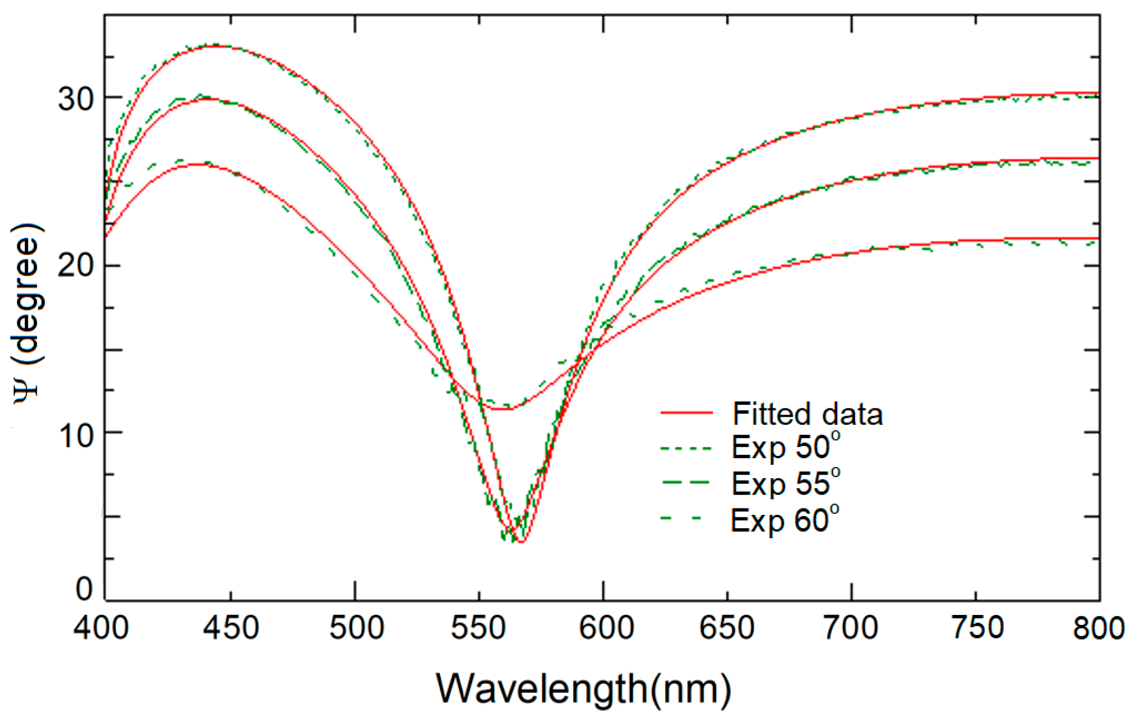
2.2. Sample Characterization

The transmittance of samples on glass substrates was examined with the Varian Cary 5E spectrometer (Varian, Palo Alto, CA, USA) at wavelengths (λ) of 250~700 nm in the UV to VIS range. For samples on silicon substrates, their surface morphology was characterized by scanning electron microscope (SEM) (S-4800, HITACHI, Krefeld, Germany) and atomic force microscope (AFM) (Digital Instruments, Bresso, Italy). Their crystallinity and composition were analyzed with X-ray diffraction (XRD) (MultiFlex, RIGAKU, Tokyo, Japan) and X-ray photoelectron spectroscopy (XPS) (ESCA PHI 1600, ULVAC-PHI, Kanagawa, Japan), respectively. Optical properties, including refractive index (n) and extinction coefficient (k) together with film thickness (d), were measured by the VASE M44 ellipsometer (J.A. Woollam Co., Lincoln, NE, USA). The deposited film on the sample’s surface was irradiated by incident light from 350 to 700 nm at incident angles of 50°, 55°, and 60°. The Ψ and Δ values of the deposited film were obtained experimentally by the ellipsometer. These values were related to the Fresnel reflection coefficients for the p- and s-polarized light, Rp and Rs, respectively, as tan(Ψ)e = Rp/Rs. The built-in Cauchy model was then used to fit the data with the following equations:
n(λ) = A + B2 + C4, and k(λ) = DeE(12400(1/λ − 1/F)),
where A~F are fitting parameters. With measured (Ψexp and Δexp) and modeled (Ψmodel and Δmodel) values, the mean squared error (MSE) can be calculated to indicate the quality of the estimator:
MSE = 1 2 N M i = 1 N Ψ i model Ψ i exp σ Ψ , i exp 2 + Δ i model Δ i exp σ Δ , i exp 2 ,
where N is the number of measured (Ψ, Δ) pairs, M is the number of fitting parameters, and σ is the standard deviation of experimentally derived Ψ or Δ [26]. Moreover, since the surface roughness of AIP-deposited films is large, another built-in model, the fitted surface roughness layer on the film’s top, was added to the Cauchy model. This roughness layer is treated as an effective medium approximation (EMA) of 50% material and 50% void [36].
In addition to optical properties, the bandgap energy of these films can also be derived from the Tauc-Lorentz (TL) model of the generalized oscillator layer model built into the ellipsometer. The imaginary part of the dielectric function (ε2 = 2nk) at a photon energy of E can be expressed as:
ε 2 = A E E g 2 C E 0 E 2 E 0 2 2 + C 2 E 2   for   E > E g   and   ε 2 = 0   for   E E g ,
where the amplitude of the oscillator A, the broadening parameter C, the peak in the joint density of states E0, and the bandgap energy Eg are four parameters to be fitted [26,37].
The photocatalytic performance of samples was evaluated by the degradation of methylene blue (MB), a prevalent test pollutant in photocatalysis [38,39], under lights of specific wavelengths. The Beer–Lambert law states that the absorbance (A) of a material to a specific light is proportional to the absorption coefficient of the material (α), the path length of the light (x), and the concentration of the material (c): A = αxc [40,41]. This absorbance is related to the transmittance (T) of the light to the same material as A = −logT. Therefore, as the photocatalytic efficiency increases, more methylene blue molecules are decomposed, leading to a decrease in their concentration. This in turn reduces the absorbance of the light. To perform photocatalytic tests, TiO2 samples of 20 mg were added to 100 mL of 10 mg/L of MB solution inside a cuvette. After exposure to light of different wavelengths (420, 440, 460, 480, and 500 nm) emitted by a photoluminescence system for 30 min, the absorbance was measured with the Varian Cary 5E spectrometer. The difference in the absorbance (ΔA) before and after the photocatalysis was calculated. The higher value of ΔA indicates more MB molecules decomposed, the better photocatalytic performance.

3. Results and Discussion

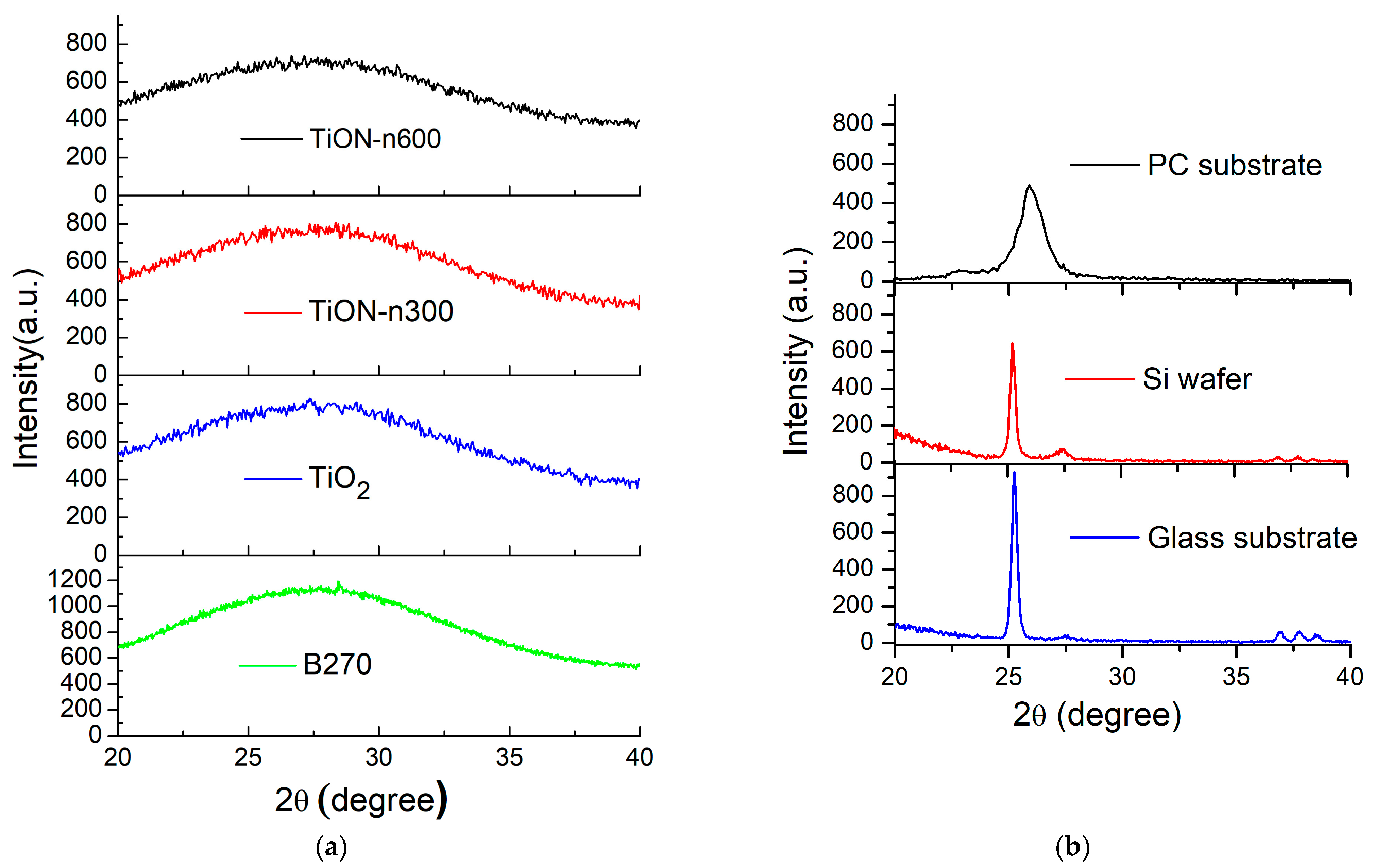
3.1. XRD and Surface Morphologies of N-Doped TiO2 Films

In the present study, TiO2 films were prepared using AIP without substrate heating. As reported, the crystal phases of TiO2 are anatase and rutile at 400 and 700 °C, respectively [13]. Figure 1a shows the XRD patterns of pure TiO2 films on silicon and B270 glass substrates and N-doped TiO2 films on silicon substrates. Clearly, all samples exhibit amorphous structures, as suggested by Karunagaran et al. that the structures of TiO2 films deposited at ambient temperature were amorphous [42]. Another possible reason is that these films are so thin (thickness ~200 nm, as discussed below) that the granular sizes are too small to form observable crystal structures. In our other study, the TiO2 film was deposited on a PC plastic substrate using AIP without substrate heating. The TiO2 film illustrates the anatase crystal structure, where the XRD peak locates at 2θ of about 25.271 degrees (Pattern COD 5000223), as shown in Figure 1b. The peak’s FWHM (Full width at half maximum) is apparently more significant than those deposited on silicon wafers and glass substrates with a substrate temperature of 250 °C. The grand size, evaluated by the Scherrer equation, of TiO2 without substrate heating is smaller than that with substrate heating. Substrate temperature does affect the growth of TiO2 crystals during AIP deposition. Nevertheless, these films fabricated without substrate heating still work as good photocatalysts in this study.

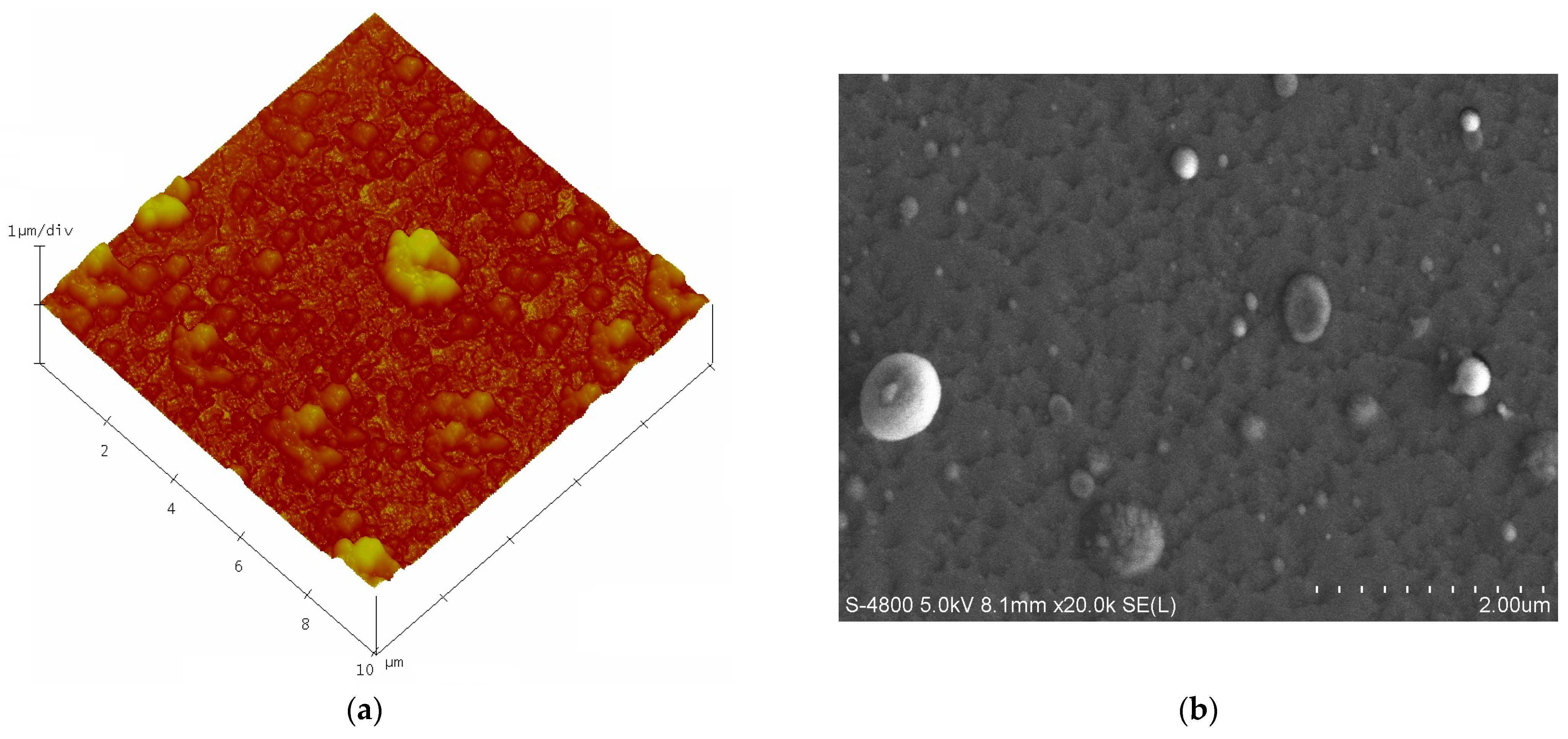
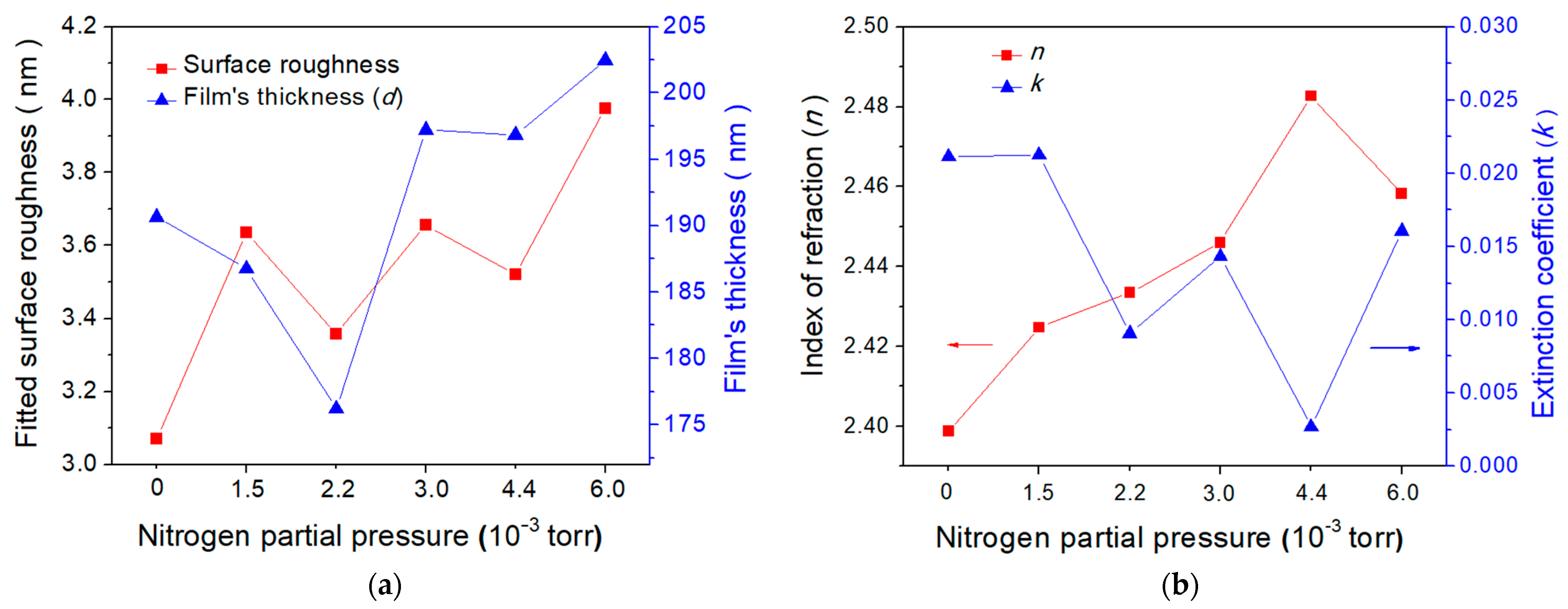
3.2. Surface Morphology of N-Doped TiO2 Films

The surface morphology of the deposited TiO2 film was characterized by AFM and SEM. The surface roughness of the AIP-deposited film shown in Figure 2a was larger than that of a film prepared with sputtering [26]. Tiny particles with sizes ranging from 0.3–0.8 μm are distributed on the surface, and the maximum particle size is about 4 μm, as shown in Figure 2b. Moreover, the samples have many tiny particles in the AIP-deposited film. The surface area of the resulting particle is more significant than the film fabricated by the other vacuum deposited method. That can strengthen the photocatalysis effect.

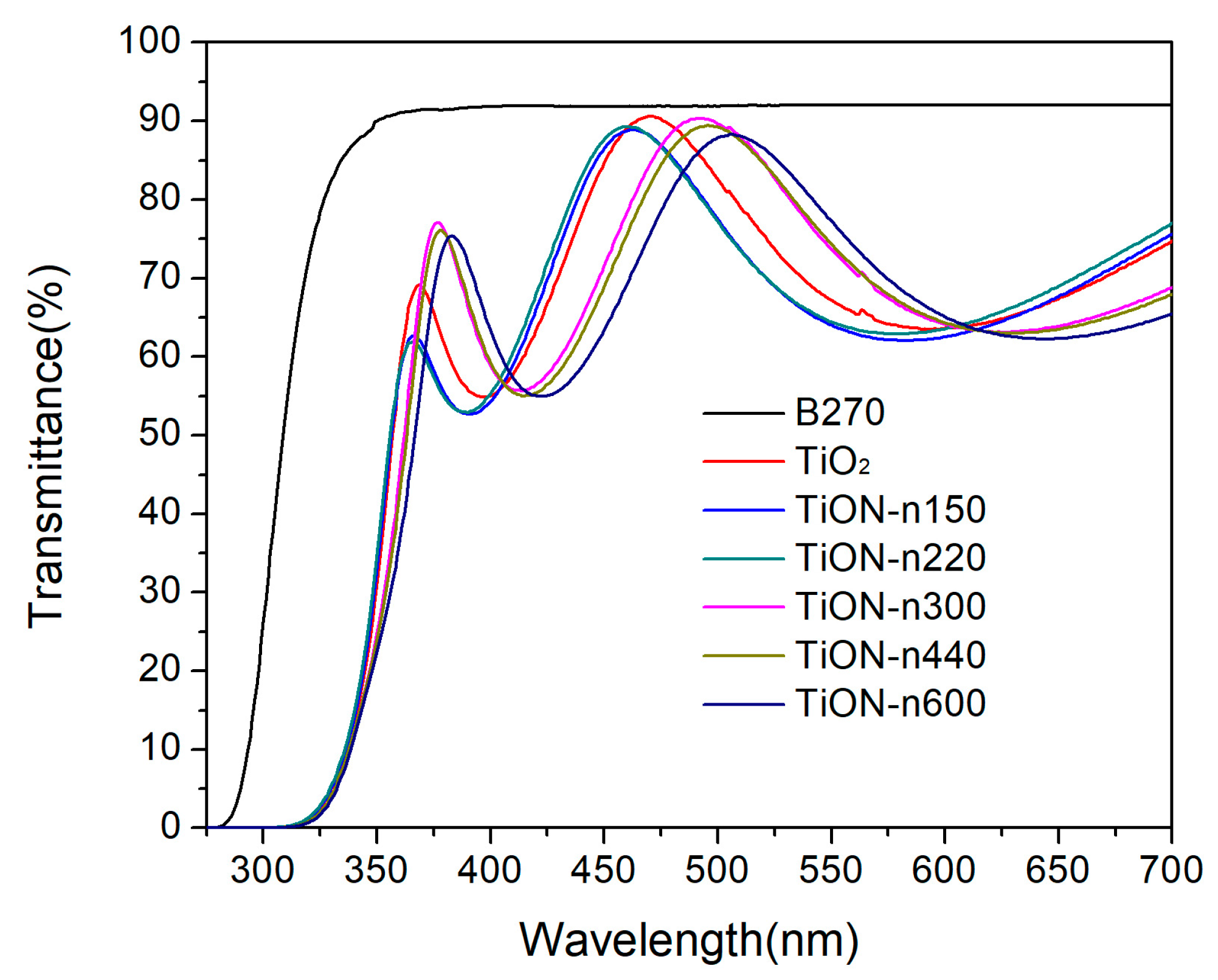
3.3. Transmittance of N-Doped TiO2 Films

The transmittance of samples on glass substrates was measured with the Varian Cary 5E spectrometer. For films on silicon substrates, the ellipsometer was used to measure the Ψ and Δ values for fitting their optical properties, including n, k, and thickness d. Figure 3 shows the transmittance in the 250~700 nm region for all samples in Table 1. With a deposition time of 120 s, the thicknesses of samples TiO2, TiON-n150, TiON-n220, TiON-n300, TiON-n440, and TiON-n600 are about 191, 187, 176, 197, 197, and 202 nm, respectively. The transmittance for all samples in the second peak in the VIS region is higher than 85%. Moreover, sample TiON-n300 (pink color) has good transmittance at 360 and 500 nm. The threshold wavelengths of all samples are around 315 nm. The different spectrum shifting, resulting from the variation of the deposited film’s optical thickness (n × d), is discussed in the following section.

3.4. Optical Properties of N-Doped TiO2 Films

The VASE M44 ellipsometer with built-in simulation models was used to derive the optical properties of N-doped TiO2 films. For example, Figure 4 shows the fitted results of the deposited TiO2 film on a silicon substrate by the Cauchy model. Measured and fitted Ψ values are shown as dashed and solid lines with an MSE value of 1.98 for three different incident angles of 50°, 55°, and 60°. The fitted thickness of the TiO2 film is 188 nm, and the top surface roughness layer is fitted to be 3.76 nm due to its rough surface mentioned in Section 3.2.
Figure 5a shows the films’ fitted surface roughness and thickness under different PN2. The thickness generally increases with increasing pressure due to crystal grain growth. The TiON-n220 sample deposited at a PN2 of 2.2 × 10⁻³ torr has the smallest fitted surface roughness, as it may have the densest grown grains. The refractive index (n) and extinction coefficient (k) at 550-nm wavelength are plotted against the N2 partial pressure in Figure 5b. The refractive index approximately increases with increasing N2 pressure, being 2.3988, 2.4247, 2.4334, 2.446, and 2.4826 at PN2 of 0, 1.5 × 10⁻³, 2.2 × 10⁻³, 3.0 × 10⁻³, 4.4 × 10⁻³, and 6.0 × 10⁻³ torr, respectively. As mentioned in Section 3.1, the grain growth due to the increased deposited thickness may increase the refractive index by reducing grain boundaries and voids in the film. However, no apparent trend exists between the Cauchy model-fitted extinction coefficient (k) and the PN2.

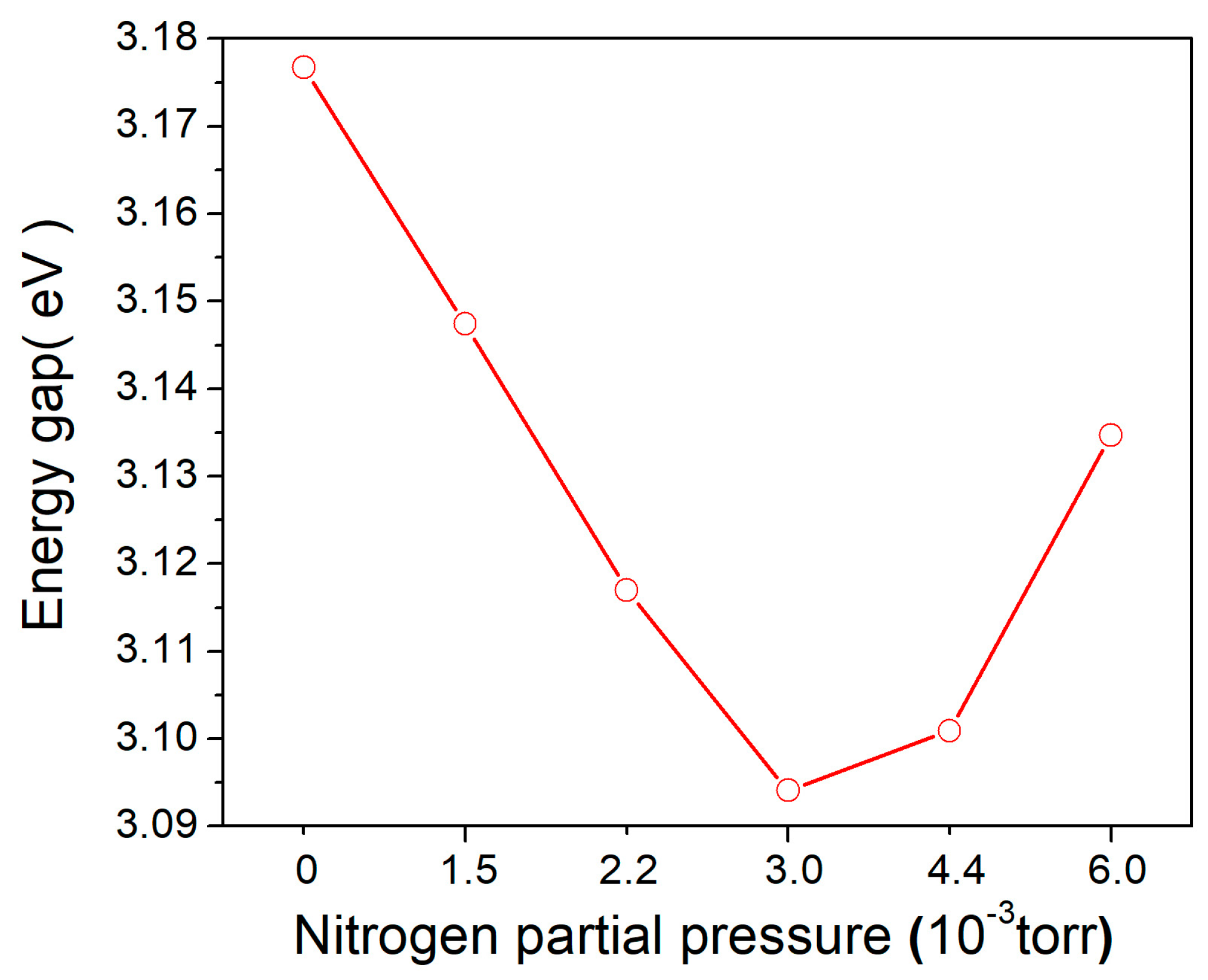
3.5. Bandgap Energy of N-Doped TiO2 Films

To increase the photocatalytic efficiency of TiO2, the optical bandgap can be reduced by N-doping. With this doping, the O vacancy state serves as an efficient generation-recombination center, and the N 2p-doped state above the valence band mixes with the O 2p valence band to narrow the bandgap [43]. However, the absorption bandgaps of nitrogen-doped TiO2 films, which have polycrystalline structures, are difficult to be determined due to the smooth transmittance curves shown in Figure 3 at the threshold wavelength of 315 nm. For the same reason, their extinction coefficients (k) fitted by the Cauchy model in Section 3.4 are somewhat disorderly with increasing N2 partial pressure, as shown in Figure 5a. The k values may also be disorderedly transformed into absorption coefficients by α = 4πk/λ equation and energy gaps.
Jellison and Modine developed the TL model in 1996. It models the dielectric function of many different amorphous materials and measures its energy gap well [44]. In this study, the N-doped TiO2 films are similar to amorphous ones due to their multi-crystalline structures of tiny crystalline grains, as mentioned in Section 3.1. Therefore, the measured Ψ values of all samples were fitted again with the TL model. For three different incident angles of 50°, 55°, and 60°, the Ψ values fitted by the TL model are somewhat like those of Ψ (solid line) fitted by the Cauchy model shown in Figure 4.
The energy gaps Egs of all samples were derived from the TL model of the generalized oscillator layer model shown in Equation (3) and plotted in Figure 6. The bandgap of the AIP-fabricated film without doping is about 3.18 eV, similar to the anatase TiO2. The energy gap decreases with increasing N2 partial pressure to 2.2 × 10⁻³ torr, being 3.15, 3.12, and 3.09 eV for PN2/PO2 = 1/9, 1/5.8, and 1/4, respectively. However, with further increased N2 partial pressure, the gap energy increases again to 3.1 and 3.13 eV for PN2/PO2 = 1/2.4 and 1/1.5, respectively. The red shift was observed with increasing N2 partial pressure from 0 to 3 × 10⁻³ torr (TiON-n300). Yang et al. applied first-principles density functional theory to study N-doped TiO2 crystals with various nitrogen concentrations and found that the red shift observed in the experiments was related to the locations of N 2p states [45]. With the sol–gel method, Cheng et al. synthesized N-doped TiO2 nano-photocatalysts in the presence of ammonium chloride. After N-doping, the light absorption edge red-shifted to the VIS region, enhancing VIS-light photocatalytic activity [46]. The red shift phenomenon was also observed in other doped TiO2 [47,48,49]. The results suggest that the N-doped TiO2 film TiON-n300 fabricated by AIP in a gaseous mixture of N2 and O2 with PN2/PO2 = 1/4 could achieve the narrowest 3.09 eV bandgap and highest absorbance in the VIS region of around 400.7 nm.
The absorbance spectra derived from the TL-mode are shown in Figure 7, indicating that compared with other samples, the spectrum of the TiON-n300 sample shifted obviously to the VIS region. These results suggest that the N-doped TiO2 film fabricated by AIP in a gaseous mixture of N2 and O2 with PN2/PO2 = 1/4 can attain the narrowest bandgap and the highest absorbance in the VIS region.

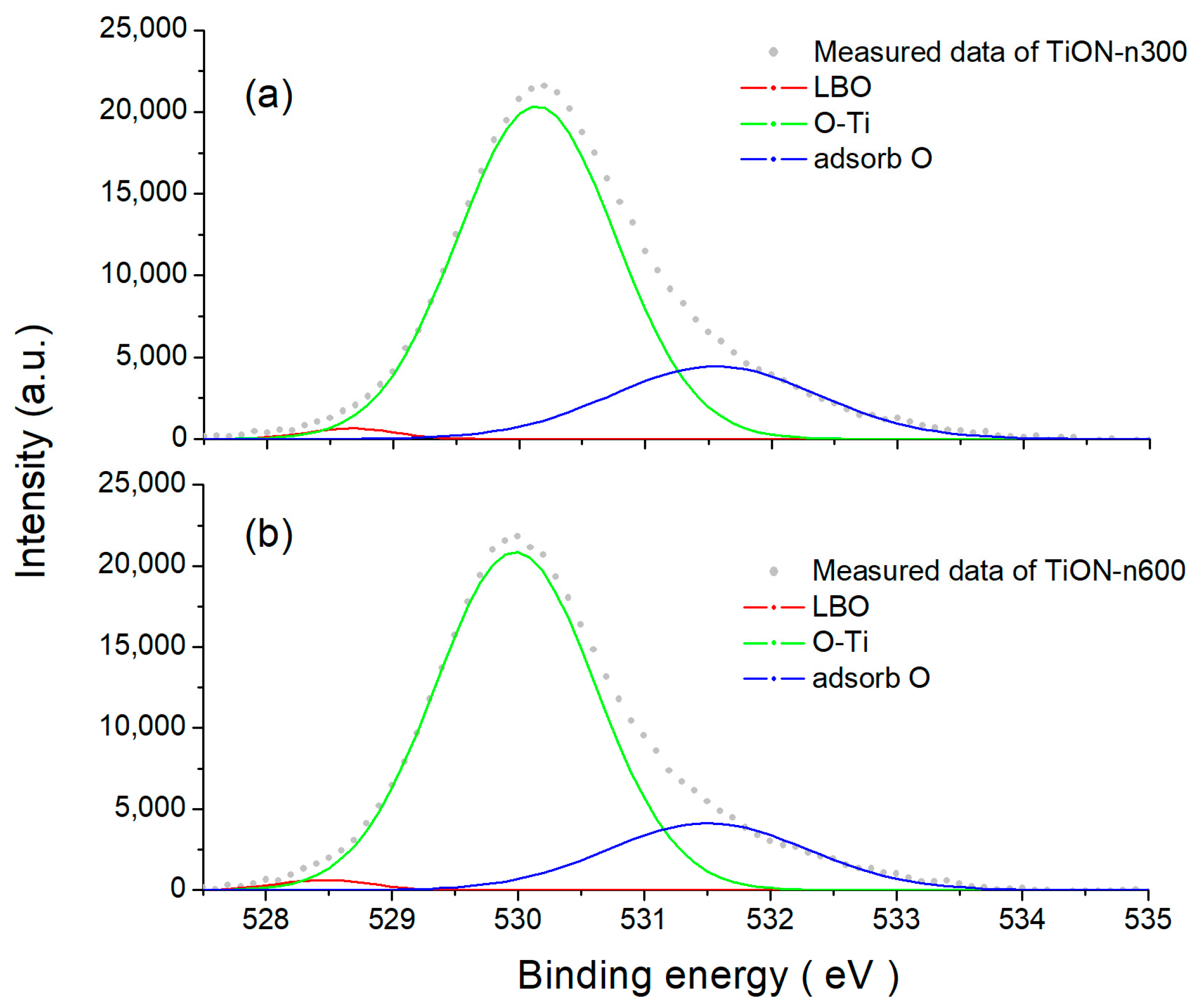
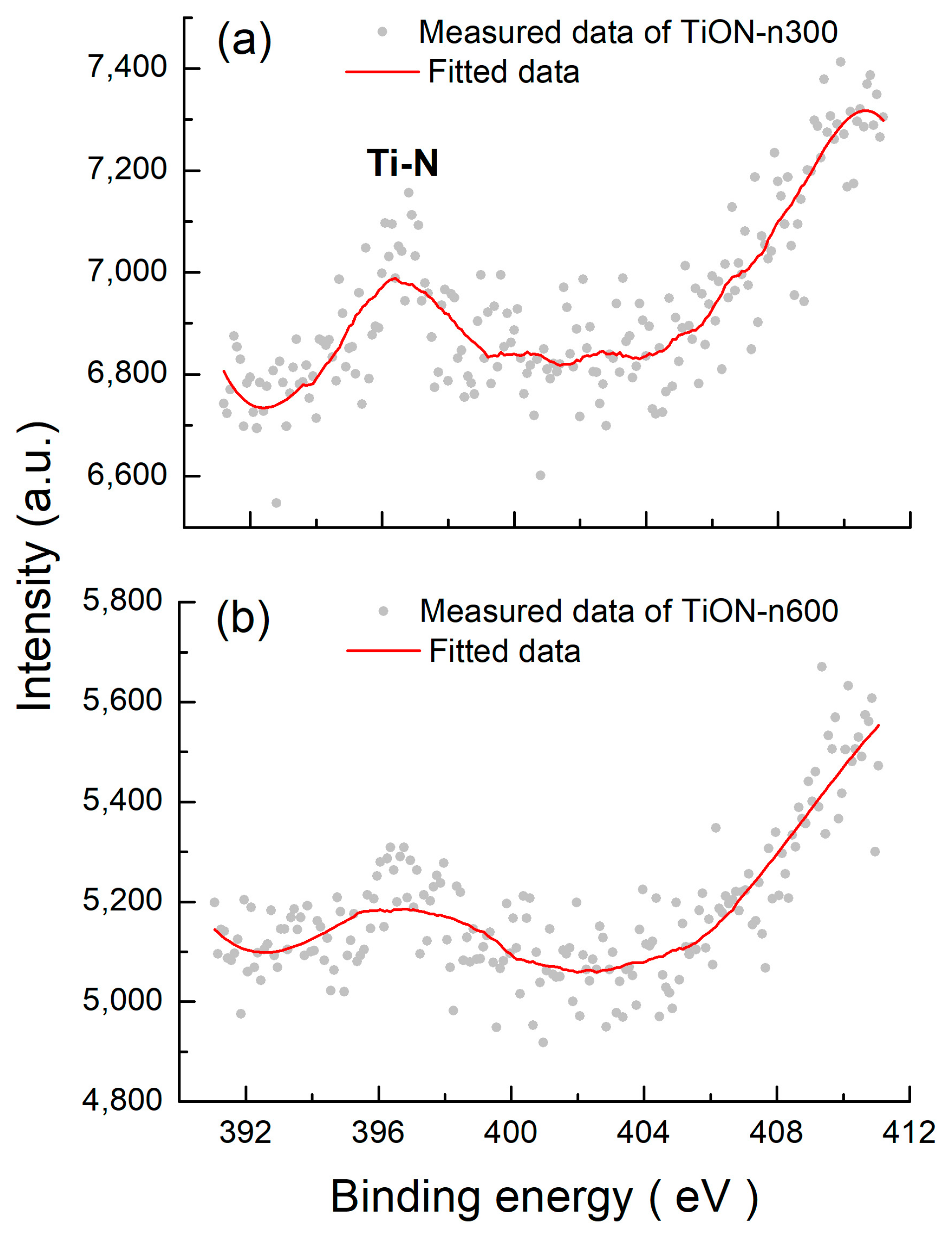
3.6. XPS of N-Doped TiO2 Films

In order to further investigate the phenomenon that the N-doped TiO2 film with PN2/PO2 = 1/4 exhibits the best photocatalytic performance, XPS of samples TiON-n300 and TiON-n600, deposited with PN2/PO2 = 1/4, 1/1.5, respectively, were conducted to evaluate their compositions. Figure 8 shows the XPS spectra of oxygen for the samples, with peaks ranging between 528 and 534 eV. Typical peaks near 528.4, 529.8, and 531.5 eV are observed. The strongest 529.8 eV peak corresponds to the O–Ti binding [50], and the much weaker 528.4 eV one represents the low-binding-energy (LBO) oxygen originating from those non-bridging oxygen (NBO) species [44]. Hsu et al. suggested that the bond at the non-bridging sites reduced the total energy of the oxide formation. The concentration of LBO in the TiO2 film was always the smallest among all components [51]. The 531.5 eV peak is from the oxygen absorption of C–O and H2O, which may come from the air and organic pollution [52].
The XPS spectra of Ti for both samples are shown in Figure 9. These signals comprise two groups, the stronger one from Ti 2p3/2 and the weaker one from Ti 2p1/2. Each group can be decomposed into three peaks of Ti2+, Ti3+, and Ti4+. For example, in the Ti 2p3/2 group, the 457 eV and 458.7 eV peaks correspond to the Ti3+ and Ti4+ bonds. The most apparent Ti4+ peak (the blue ones) originates from the normal TiO2. When O2 molecules are less, three O atoms share two Ti atoms, forming Ti2O3 and the weaker Ti3+ peak (the green ones). The Ti3+ peak of TiON-n300 shown in Figure 9a is weaker than that of TiON-n600 shown in Figure 9b. It explains that the transmittance of TiON-n300 is better than that of TiON-n600 shown in Figure 3. The 456 eV Ti2+ peaks (the red ones) come from the Ti–N bonds [52]. Although the PN2 is higher in the TiON-n600 sample, the Ti–N bond is somewhat weaker than that in the TiON-n300 sample. It explains why the TiON-n300 sample exhibits the narrowest energy gap and the best photocatalytic performance.
Figure 10 shows the XPS spectra of N for both samples. The TiON-n300 sample exhibits a clear 396.7 eV peak from the Ti–N bond, as shown in Figure 10a [53]. The intensity of this peak is reduced in the TiON-n600 sample, as shown in Figure 10b. It again verifies that the TiON-n300 sample has the narrowest energy gap and the highest photocatalytic efficiency due to the light absorption of the Ti–N bond.

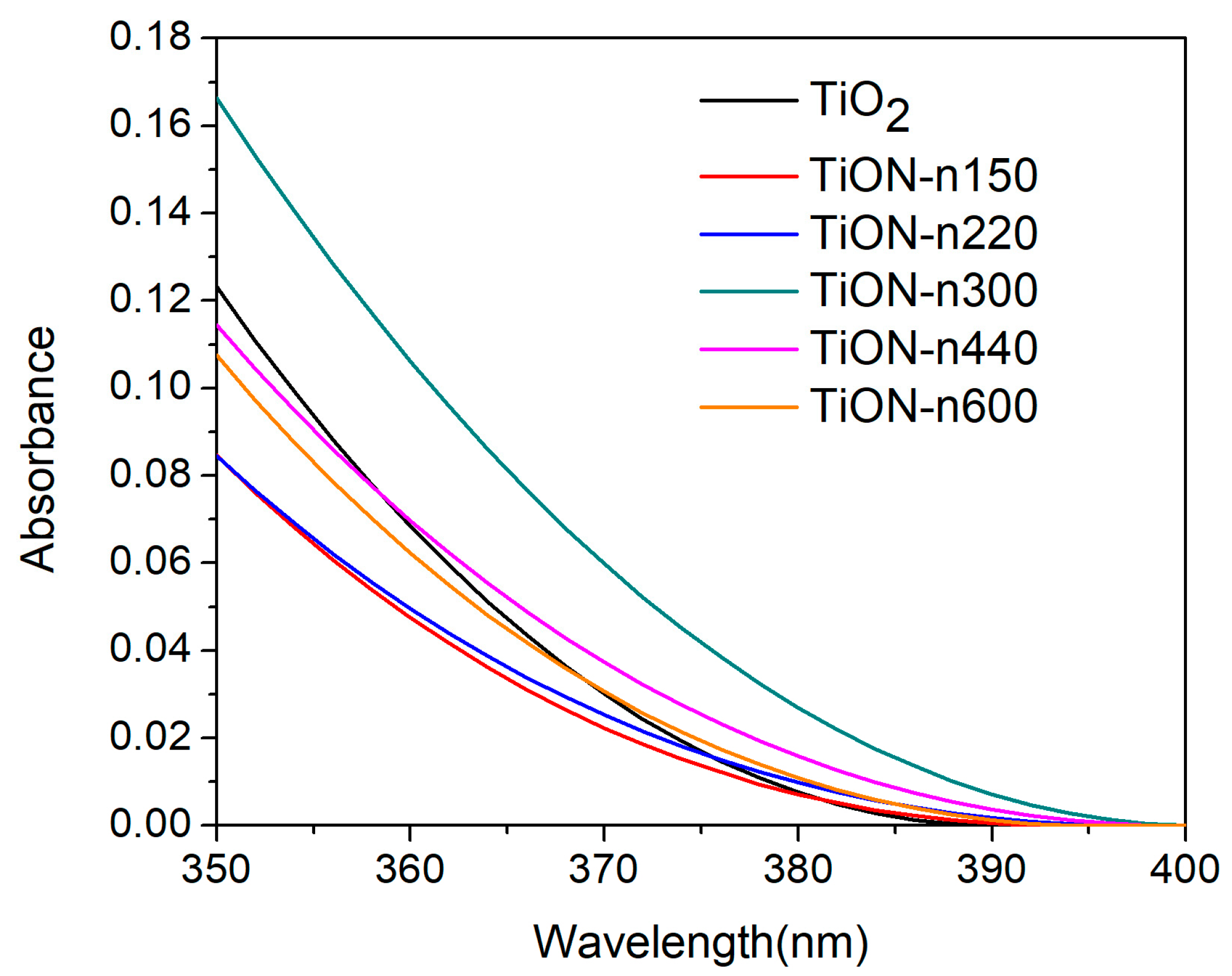
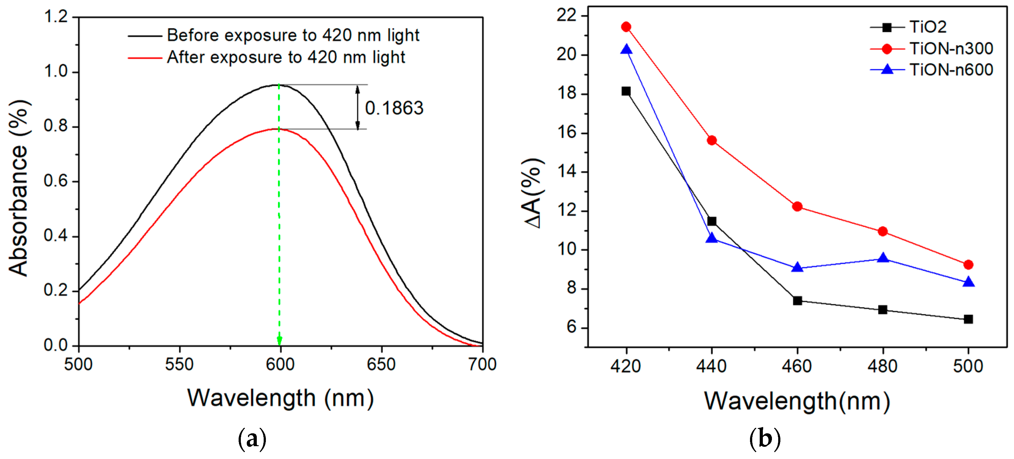
3.7. Photocatalytic Performance of N-Doped TiO2 Films

The degradation of MB is used to evaluate the photocatalytic performance of N-doped TiO2 films. As the photocatalytic efficiency increases, more MB molecules are decomposed, leading to a decrease in their concentration. According to the Beer–Lambert law, this in turn reduces the absorbance to the light measured at 600 nm since MB exhibits the highest absorbance at this wavelength. Figure 11a shows the absorbance of the pure TiO2 sample in the MB solution before and after exposure to 420 nm light. The efficiencies are qualitatively analyzed by calculating the absorbance difference, such as 0.1863% shown in Figure 11a, before and after the MB solution is reacted with the chosen sample under the exposure of varying photocatalytic light sources. Figure 11b shows ΔA, the absorbance difference divided by the peak value of the absorbance spectrum before exposure, of the samples pure TiO2, TiON-n300, and TiON-n600 in percentage for exposure to photocatalytic lights at 420, 440, 460, 480, and 500 nm wavelength, respectively. As increasing the wavelength, the ΔA value decreases, indicating worse photocatalytic performance. However, the performance of TiON-n600 appears better than that of the pure TiO2 film at excitation wavelengths of 460, 480, and 500 nm. The nitrogen dopant indeed reduces the photocatalytic bandgap. Among these samples, TiON-n300 shows the largest ΔA and hence the highest photocatalytic efficiency, verifying that it has the narrowest bandgap.
Table 2 compares nitrogen-doped TiO2 films prepared at different parameters of substrate temperature and negative bias in other studies. In the present work, the samples deposited at no bias and substrate heating exhibited amorphous structures. At PN2/PO2 = 1/4 condition, the nitrogen-doped TiO2 film showed the best photocatalytic performance.

4. Conclusions

N-doped TiO2 films were prepared by AIP under various gas mixing ratios without substrate heating and/or applied bias. The N-doping led to a similar amorphous structure of these films with rough surfaces. Analysis of their transmittance, optical properties, and bandgap energies indicated that the N-doped TiO2 film with the PN2/PO2 ratio of 1/4 could attain the narrowest bandgap and the highest absorbance in the VIS region. This narrowest gap corresponded to the best photocatalytic performance, as verified by the MB test. Moreover, the sample’s Ti and N XPS spectra exhibited prominent Ti–N peaks, responsible for its narrowest energy gap and highest photocatalytic efficiency. These results conclude that AIP can prepare the N-doped TiO2 film without substrate heating, and at a certain PN2/PO2 ratio, the bandgap can be efficiently reduced to enhance its photocatalytic ability. This study further explains the mechanisms of N-doped TiO2 photocatalysts without substrate heating. The result can be considered for the photocatalysts deposition of heat-labile substrates.

Author Contributions

Conceptualization, J.-C.H.; methodology, W.-C.H. and J.-C.H.; software, W.-C.H. and G.-Y.Y.; validation, Y.-S.S.; formal analysis, J.-L.W. and G.-Y.Y.; investigation, J.-L.W.; resources, J.-L.W.; data curation, W.-C.H. and H.-Y.W.; writing—original draft preparation, Y.-S.S. and H.-Y.W.; writing—review and editing, H.-Y.W. and J.-C.H.; visualization, J.-C.H.; supervision, Y.-S.S. and J.-C.H.; project administration, W.-C.H. and G.-Y.Y.; funding acquisition, H.-Y.W. All authors have read and agreed to the published version of the manuscript.

Funding

This research was funded by the Ministry of Science and Technology of Taiwan, grant numbers MOST 111-2112-M-030-004 and MOST 111-2221-E-030-007.

Institutional Review Board Statement

Not applicable.

Informed Consent Statement

Not applicable.

Acknowledgments

We thank the Ming Chi University of Technology who supported the FESEM, XPS, and XRD experimental work.

Conflicts of Interest

The authors declare no conflict of interest.

References

  1. Yang, X.G.; Wang, D.W. Photocatalysis: From fundamental principles to materials and applications. Acs Appl. Energ. Mater. 2018, 1, 6657–6693. [Google Scholar] [CrossRef]
  2. Ibhadon, A.O.; Fitzpatrick, P. Heterogeneous photocatalysis: Recent advances and applications. Catalysts 2013, 3, 189–218. [Google Scholar] [CrossRef] [Green Version]
  3. Wenderich, K.; Mul, G. Methods, mechanism, and applications of photo deposition in photocatalysis: A review. Chem. Rev. 2016, 116, 14587–14619. [Google Scholar] [PubMed]
  4. Sun, Y.; O’Connell, D.W. Application of visible light active photocatalysis for water contaminants: A review. Water Environ. Res. 2022, 94, e10781. [Google Scholar] [CrossRef] [PubMed]
  5. Elgohary, E.A.; Mohamed, Y.M.A.; El Nazer, H.A.; Baaloudj, O.; Alyami, M.S.S.; El Jery, A.; Assadi, A.A.; Amrane, A. A review of the use of semiconductors as catalysts in the photocatalytic inactivation of microorganisms. Catalysts 2021, 11, 1498. [Google Scholar] [CrossRef]
  6. Zhang, L.P.; Ran, J.R.; Qiao, S.Z.; Jaroniec, M. Characterization of semiconductor photocatalysts. Chem. Soc. Rev. 2019, 48, 5184–5206. [Google Scholar] [CrossRef] [PubMed]
  7. Serpone, N.; Emeline, A.V. Semiconductor photocatalysis–past, present, and future outlook. J. Phys. Chem. Lett. 2012, 3, 673–677. [Google Scholar] [CrossRef]
  8. Areeshi, M.Y. A review on biological synthesis of ZnO nanostructures and its application in photocatalysis mediated dye degradation: An overview. Luminescence 2022. [Google Scholar] [CrossRef]
  9. Arun, J.; Nachiappan, S.; Rangarajan, G.; Alagappan, R.P.; Gopinath, K.P.; Lichtfouse, E. Synthesis and application of titanium dioxide photocatalysis for energy, decontamination and viral disinfection: A review. Environ. Chem. Lett. 2023, 21, 339–362. [Google Scholar] [CrossRef]
  10. Yan, H.; Wang, X.D.; Yao, M.; Yao, X.J. Band structure design of semiconductors for enhanced photocatalytic activity: The case of TiO2. Prog. Nat. Sci. Mater. 2013, 23, 402–407. [Google Scholar] [CrossRef]
  11. Nagaveni, K.; Hegde, M.S.; Ravishankar, N.; Subbanna, G.N.; Madras, G. Synthesis and structure of nano-crystalline TiO2 with lower band gap showing high photocatalytic activity. Langmuir 2004, 20, 2900–2907. [Google Scholar] [CrossRef]
  12. Pawar, M.; Sendogdular, S.T.; Gouma, P. A brief overview of TiO2 photocatalyst for organic dye remediation: Case study of reaction mechanisms involved in Ce-TiO2 photocatalysts system. J. Nanomater. 2018, 2018, 5953609. [Google Scholar] [CrossRef] [Green Version]
  13. Wu, H.Y.; Lin, H.C.; Liu, Y.H.; Chen, K.L.; Wang, Y.H.; Sun, Y.S.; Hsu, J.C. Highly sensitive, robust, and recyclable TiO2/AgNP substrate for SERS detection. Molecules 2022, 27, 6755. [Google Scholar] [CrossRef] [PubMed]
  14. Wang, S.; Yang, X.J.; Jiang, Q.; Lian, J.S. Enhanced optical absorption and photocatalytic activity of Cu/N-codoped TiO2 nanocrystals. Mat. Sci. Semicon. Proc. 2014, 24, 247–253. [Google Scholar] [CrossRef]
  15. Ansari, S.A.; Cho, M.H. Highly visible light responsive, narrow band gap TiO2 nanoparticles modified by elemental red phosphorus for photocatalysis and photoelectrochemical applications. Sci. Rep. 2016, 6, 25405. [Google Scholar] [CrossRef] [PubMed] [Green Version]
  16. Pitre, S.P.; Yoon, T.P.; Scaiano, J.C. Titanium dioxide visible light photocatalysis: Surface association enables photocatalysis with visible light irradiation. Chem. Commun. 2017, 53, 4335–4338. [Google Scholar] [CrossRef] [Green Version]
  17. Pant, B.; Park, M.; Park, S.J. Recent advances in TiO2 films prepared by sol-gel methods for photocatalytic degradation of organic pollutants and antibacterial activities. Coatings 2019, 9, 613. [Google Scholar] [CrossRef] [Green Version]
  18. Wang, Y.H.; Rahman, K.H.; Wu, C.C.; Chen, K.C. A review on the pathways of the improved structural characteristics and photocatalytic performance of titanium dioxide (TiO2) thin films fabricated by the magnetron-sputtering technique. Catalysts 2020, 10, 598. [Google Scholar] [CrossRef]
  19. Patil, M.K.; Shaikh, S.; Ganesh, I. Recent advances on TiO2 thin film based photocatalytic applications (a review). Curr. Nanosci. 2015, 11, 271–285. [Google Scholar] [CrossRef]
  20. Hao, B.F.; Guo, J.P.; Zhang, L.; Ma, H.Z. Magnetron sputtered TiO2/CuO heterojunction thin films for efficient photocatalysis of rhodamine B. J. Alloys Compd. 2022, 903, 163851. [Google Scholar] [CrossRef]
  21. Becker, M.; Yezerska, O. Review-recent progress in low temperature synthesis of crystalline TiO2 photocatalytic films by highly controllable electrodeposition. J. Electrochem. Soc. 2022, 169, 052507. [Google Scholar] [CrossRef]
  22. Asahi, R.; Morikawa, T.; Ohwaki, T.; Aoki, K.; Taga, Y. Visible-light photocatalysis in nitrogen-doped titanium oxides. Science 2001, 293, 269–271. [Google Scholar] [CrossRef] [PubMed]
  23. Akhter, P.; Arshad, A.; Saleem, A.; Hussain, M. Recent development in non-metal-doped titanium dioxide photocatalysts for different dyes degradation and the study of their strategic factors: A review. Catalysts 2022, 12, 1331. [Google Scholar] [CrossRef]
  24. Temam, E.G.; Djani, F.; Rahmane, S.; Ben Temam, H.; Gasmi, B. Photocatalytic activity of Al/Ni doped TiO2 films synthesized by sol-gel method: Dependence on thickness and crystal growth of photocatalysts. Surf. Interfaces 2022, 31, 102077. [Google Scholar] [CrossRef]
  25. Tang, W.M.; Hu, C.C.; Tsao, C.C.; Chen, C.S.; Roselin, L.S.; Kuo, C.G.; Hsu, C.Y. Photocatalytic activity and mechanical performance of o and n co-doped tio2 thin films. J. Electron. Mater. 2022, 51, 6145–6159. [Google Scholar] [CrossRef]
  26. Hsu, J.C.; Lin, Y.H.; Wang, P.W. X-ray photoelectron spectroscopy analysis of nitrogen-doped TiO2 films prepared by reactive-ion-beam sputtering with various NH3/O2 gas mixture ratios. Coatings 2020, 10, 47. [Google Scholar] [CrossRef] [Green Version]
  27. Zhao, Z.; Liu, Q. Mechanism of higher photocatalytic activity of anatase TiO2 doped with nitrogen under visible-light irradiation from density functional theory calculation. J. Phys. D Appl. Phys. 2008, 41, 025105. [Google Scholar] [CrossRef]
  28. Irie, H.; Watanabe, Y.; Hashimoto, K. Nitrogen-concentration dependence on photocatalytic activity of TiO2-xNx powders. J. Phys. Chem. B 2003, 107, 5483–5486. [Google Scholar] [CrossRef]
  29. Ihara, T.; Miyoshi, M.; Iriyama, Y.; Matsumoto, O.; Sugihara, S. Visible-light-active titanium oxide photocatalyst realized by an oxygen-deficient structure and by nitrogen doping. Appl. Catal. B Environ 2003, 42, 403–409. [Google Scholar] [CrossRef]
  30. Lindgren, T.; Mwabora, J.M.; Avendano, E.; Jonsson, J.; Hoel, A.; Granqvist, C.G.; Lindquist, S.E. Photoelectrochemical and optical properties of nitrogen doped titanium dioxide films prepared by reactive dc magnetron sputtering. J. Phys. Chem. B 2003, 107, 5709–5716. [Google Scholar] [CrossRef]
  31. Guo, Y.; Zhang, X.W.; Weng, W.H.; Han, G.R. Structure and properties of nitrogen-doped titanium dioxide thin films grown by atmospheric pressure chemical vapor deposition. Thin Solid Films 2007, 515, 7117–7121. [Google Scholar] [CrossRef]
  32. Powell, M.J.; Dunnill, C.W.; Parkin, I.P. N-doped TiO2 visible light photocatalyst films via a sol-gel route using TMEDA as the nitrogen source. J. Photochem. Photobiol. A 2014, 281, 27–34. [Google Scholar] [CrossRef]
  33. Chang, J.T.; Su, C.W.; He, J.L. Photocatalytic TiO2 film prepared using arc ion plating. Surf. Coat. Technol. 2006, 200, 3027–3034. [Google Scholar] [CrossRef]
  34. Chang, J.T.; Lai, Y.F.; He, J.L. Photocatalytic performance of chromium or nitrogen doped arc ion plated-TiO2 films. Surf. Coat. Technol. 2005, 200, 1640–1644. [Google Scholar]
  35. Zhang, M.; Lin, G.Q.; Dong, C.; Kim, K.H. Mechanical and optical properties of composite TiOxNy films prepared by pulsed bias arc ion plating. Curr. Appl. Phys. 2009, 9, S174–S178. [Google Scholar]
  36. Lehmann, D.; Seidel, F.; Zahn, D.R.T. Thin films with high surface roughness: Thickness and dielectric function analysis using spectroscopic ellipsometry. Springerplus 2014, 3, 82. [Google Scholar] [CrossRef] [PubMed] [Green Version]
  37. Eiamchai, P.; Chindaudom, P.; Pokaipisit, A.; Limsuwan, P. A spectroscopic ellipsometry study of TiO2 thin films prepared by ion-assisted electron-beam evaporation. Curr. Appl. Phys. 2009, 9, 707–712. [Google Scholar] [CrossRef]
  38. Dariani, R.S.; Esmaeili, A.; Mortezaali, A.; Dehghanpour, S. Photocatalytic reaction and degradation of methylene blue on TiO2 nano-sized particles. Optik 2016, 127, 7143–7154. [Google Scholar]
  39. Hou, C.T.; Hu, B.; Zhu, J.M. Photocatalytic degradation of methylene blue over TiO2 pretreated with varying concentrations of NaOH. Catalysts 2018, 8, 575. [Google Scholar] [CrossRef] [Green Version]
  40. Lin, F.Y.; Lin, J.Y.; Lo, K.Y.; Sun, Y.S. Use microfluidic chips to study the phototaxis of lung cancer cells. Int. J. Mol. Sci. 2019, 20, 4515. [Google Scholar] [CrossRef] [Green Version]
  41. Huang, C.H.; Hou, H.S.; Lo, K.Y.; Cheng, J.Y.; Sun, Y.S. Use microfluidic chips to study the effects of ultraviolet lights on human fibroblasts. Microfluid. Nanofluid. 2017, 21, 79. [Google Scholar] [CrossRef]
  42. Karunagaran, B.; Kumar, R.T.R.; Mangalaraj, D.; Narayandass, S.K.; Rao, G.M. Influence of thermal annealing on the composition and structural parameters of dc magnetron sputtered titanium dioxide thin films. Cryst. Res. Technol. 2002, 37, 1285–1292. [Google Scholar] [CrossRef]
  43. Nakano, Y.; Morikawa, T.; Ohwaki, T.; Taga, Y. Deep-level optical spectroscopy investigation of n-doped TiO2 films. Appl. Phys. Lett. 2005, 86, 132104. [Google Scholar] [CrossRef]
  44. Jellison, G.E., Jr.; Modine, F.A. Parameterization of the optical functions of amorphous materials in the interband region. Appl. Phys. Lett. 1996, 69, 371–373. [Google Scholar] [CrossRef]
  45. Yang, K.S.; Dai, Y.; Huang, B.B. Study of the nitrogen concentration influence on n-doped TiO2 anatase from first-principles calculations. J. Phys. Chem. C 2007, 111, 12086–12090. [Google Scholar] [CrossRef]
  46. Cheng, X.W.; Yu, X.J.; Xing, Z.P.; Yang, L.S. Synthesis and characterization of n-doped TiO2 and its enhanced visible-light photocatalytic activity. Arab. J. Chem. 2016, 9, S1706–S1711. [Google Scholar] [CrossRef]
  47. Shao, G.S. Red shift in manganese- and iron-doped TiO2: A DFT+U analysis. J. Phys. Chem. C 2009, 113, 6800–6808. [Google Scholar] [CrossRef]
  48. Zhou, W.F.; Liu, Q.J.; Zhu, Z.Q.; Zhang, J. Preparation and properties of vanadium-doped TiO2 photocatalysts. J. Phys. D Appl. Phys. 2010, 43, 035301. [Google Scholar] [CrossRef]
  49. Deng, Q.R.; Han, X.P.; Gao, Y.; Shao, G.S. Remarkable optical red shift and extremely high optical absorption coefficient of V-Ga co-doped TiO2. J. Appl. Phys. 2012, 112, 013523. [Google Scholar] [CrossRef]
  50. Trenczek-Zajac, A.; Radecka, M.; Zakrzewska, K.; Brudnik, A.; Kusior, E.; Bourgeois, S.; de Lucas, M.C.M.; Imhoff, L. Structural and electrical properties of magnetron sputtered Ti(ON) thin films: The case of TiN doped in situ with oxygen. J. Power Sources 2009, 194, 93–103. [Google Scholar] [CrossRef]
  51. Hsu, J.C.; Lee, C.C.; Chen, H.L.; Kuo, C.C.; Wang, P.W. Investigation of thin TiO2 films cosputtered with Si species. Appl. Surf. Sci. 2009, 255, 4852–4858. [Google Scholar] [CrossRef]
  52. Braic, M.; Balaceanu, M.; Vladescu, A.; Kiss, A.; Braic, V.; Epurescu, G.; Dinescu, G.; Moldovan, A.; Birjega, R.; Dinescu, M. Preparation and characterization of titanium oxy-nitride thin films. Appl. Surf. Sci. 2007, 253, 8210–8214. [Google Scholar] [CrossRef]
  53. Yu, Y.P.; Xing, X.J.; Xu, L.M.; Wu, S.X.; Li, S.W. N-derived signals in the x-ray photoelectron spectra of n-doped anatase TiO2. J. Appl. Phys. 2009, 105, 12353. [Google Scholar] [CrossRef]
  54. Zhang, S.J.; Li, M.S.; Chen, Z.Q.; Hu, J.X. Effects of N-doped quantity and current density on properties of TiO2 films by arc ion plating. Adv. Mater. Res. 2011, 345, 87–92. [Google Scholar] [CrossRef]
  55. Zhang, S.J.; Li, M.S.; Chen, Z.Q.; Fan, Y.Z. Influence of annealing treatment on N-doped TiO2 films deposited by pulsed negative bias arc ion plating. Adv. Mater. Res. 2012, 482–484, 1105–1110. [Google Scholar]
  56. Zhang, S.J.; Li, M.S.; Chen, Z.Q.; Fan, Y.Z. Effects of pulsed negative bias and current density on properties of N-doped TiO2 films deposited by arc ion plating. Adv. Mater. Res. 2012, 476–478, 2357–2362. [Google Scholar] [CrossRef]
Figure 1. (a) XRD patterns of samples TiON-n600, TiON-n300, TiO2, and B270, (b) XRD patterns of samples with 2-μm TiO2 deposited on a PC substrate without substrate heating, a silicon wafer and a glass substrate both with substrate temperature 250 °C.
Coatings 13 00654 g001
Figure 2. Surface morphology of sample TiO2 characterized by (a) AFM and (b) SEM.
Coatings 13 00654 g002
Figure 3. Transmittance in the 250~700 nm region for all samples listed in Table 1.
Coatings 13 00654 g003
Figure 4. Measured (dashed lines) and Cauchy model-fitted Ψ (solid lines) values for three different incident angles of 50°, 55°, and 60° are shown for the TiO2 film deposited on a silicon substrate.
Coatings 13 00654 g004
Figure 5. (a) Fitted surface roughness and thickness of these films under different N2 partial pressures. (b) Refractive index (n) and extinction coefficient (k) at 550-nm wavelength under different N2 partial pressures.
Coatings 13 00654 g005
Figure 6. Energy gaps of N-doped TiO2 films under different N2 partial pressures.
Coatings 13 00654 g006
Figure 7. Absorbance spectra of all samples derived from the TL model.
Coatings 13 00654 g007
Figure 8. XPS spectra of O 1s core line for samples (a) TiON-n300 and (b) TiON-n600.
Coatings 13 00654 g008
Figure 9. XPS spectra of Ti 2p core line for samples (a) TiON-n300 and (b) TiON-n600.
Coatings 13 00654 g009
Figure 10. XPS spectra of N 1s core line for samples (a) TiON-n300 and (b) TiON-n600.
Coatings 13 00654 g010
Figure 11. (a) Absorbance of pure TiO2 sample in the MB solution before and after exposure to 420 nm light. (b) Absorbance change rates of different samples in MB solution irradiated with different photon wavelengths.
Coatings 13 00654 g011
Table 1. N-doped TiO2 thin films prepared by using AIP under different N2 and O2 partial pressures.
SampleSubstrateN2 Partial Pressure, PN2 (×10−3 torr)O2 partial pressure, PO2 (×10−3 torr)PN2/PO2
TiO2Silicon015.00
TiON-n150Silicon1.513.51/9
TiON-n220Silicon2.212.81/5.8
TiON-n300Silicon3.012.01/4
TiON-n440Silicon4.410.61/2.4
TiON-n600Silicon6.09.01/1.5
Table 2. A comparison of nitrogen-doped TiO2 films prepared by arc ion plating (AIP).
Substrate ConditionsWorking PressuresMain FindingsReferences
1. No substrate bias
2. Tsub not specified (No substrate heating)
1. Ptotal = 0.8 Pa
2. PN2/Ptotal = 5%~50%
1. Amount of TiO2 anatase phase decreased with N doping.
2. N doping generally reduced photocatalytic efficacy, but the performance increased at PN2/Ptotal = 5%~10%
[34]
1. Substrate bias from 0 to −700 V
2. Tsub not specified
1. Ptotal = 0.2 Pa
2. PN2/PO2 = 1/2
1. At a bias of −100 V, these films exhibited a mixture of anatase and rutile phases.[35]
2. No substrate bias
1. Tsub = 200 °C
1. Ptotal = 1~1.3 Pa
2. PN2/PO2 = 0, 2/1~5/1
1. N doping inhibited the anatase growth and promoted rutile formation.
2. N-doped TiO2 film not only reduced the UV catalytic performance but also extended the catalytic properties to the sunlight.
[54]
1. Substrate bias from 0 to −600 V
2. Tsub = 200~300 °C
1. Ptotal = 1~1.3 Pa
2. PN2/PO2 = 13/4
1. Absorption edges of the as-deposited films are increased with the rising of the negative bias, and a maximum of 550 nm is achieved under −600 V bias.[55]
1. Substrate bias from 0 to −600 V @20 kHz
2. Tsub = 150~300 °C
1. Ptotal = 1~1.8 Pa
2. PN2/PO2 = 13/4
1. Applying the negative pulse bias extended the absorption edge 5–40 nm towards the visible region.[56]
1. No substrate bias
2. No substrate heating
1. Ptotal = 2 Pa
2. PN2/PO2 = 0, 1/9~1/1.5
1. All samples exhibited amorphous structures.
2. Sample with PN2/PO2 = 1/4 showed the best photocatalytic performance.
The present work
Tsub: substrate temperature.
Disclaimer/Publisher’s Note: The statements, opinions and data contained in all publications are solely those of the individual author(s) and contributor(s) and not of MDPI and/or the editor(s). MDPI and/or the editor(s) disclaim responsibility for any injury to people or property resulting from any ideas, methods, instructions or products referred to in the content.

