
Characterization of CdxTeyOz/CdS/ZnO Heterostructures Synthesized by the SILAR Method

 ,
,
Abstract
:1. Introduction
2. Materials and Methods
2.1. Materials and Samples for the Experiment
2.2. Synthesis Methods
- Preparation of solutions containing ions of precipitated substances;
- Immersion of the substrate in the prepared solution for the purpose of adsorption of ions;
- Washing the substrate to remove excess (non-adsorbed and weakly bound) ions from its surface;
- Drying of samples.
2.3. Characterization of Synthesised Structures
3. Results
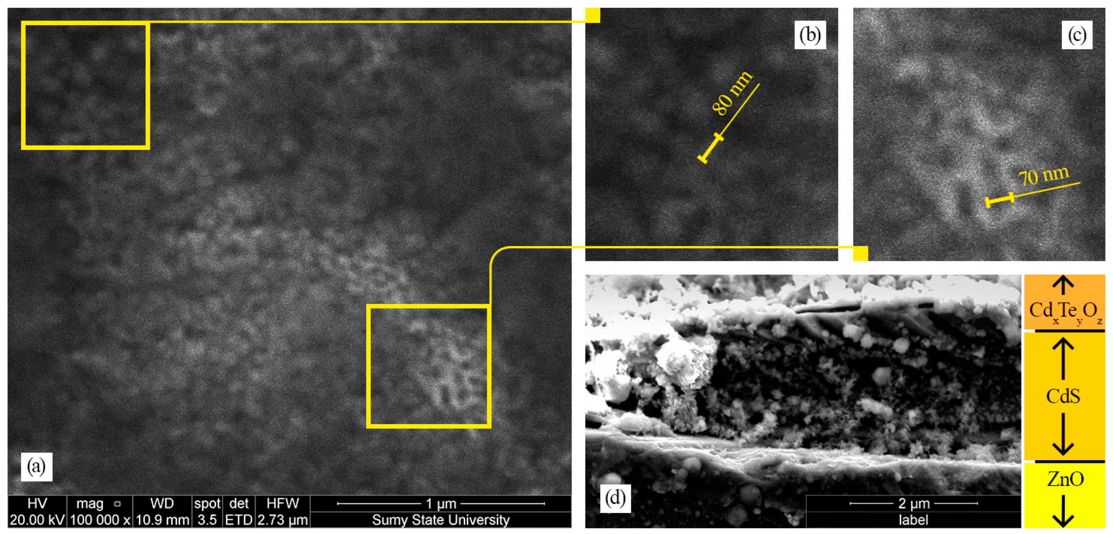
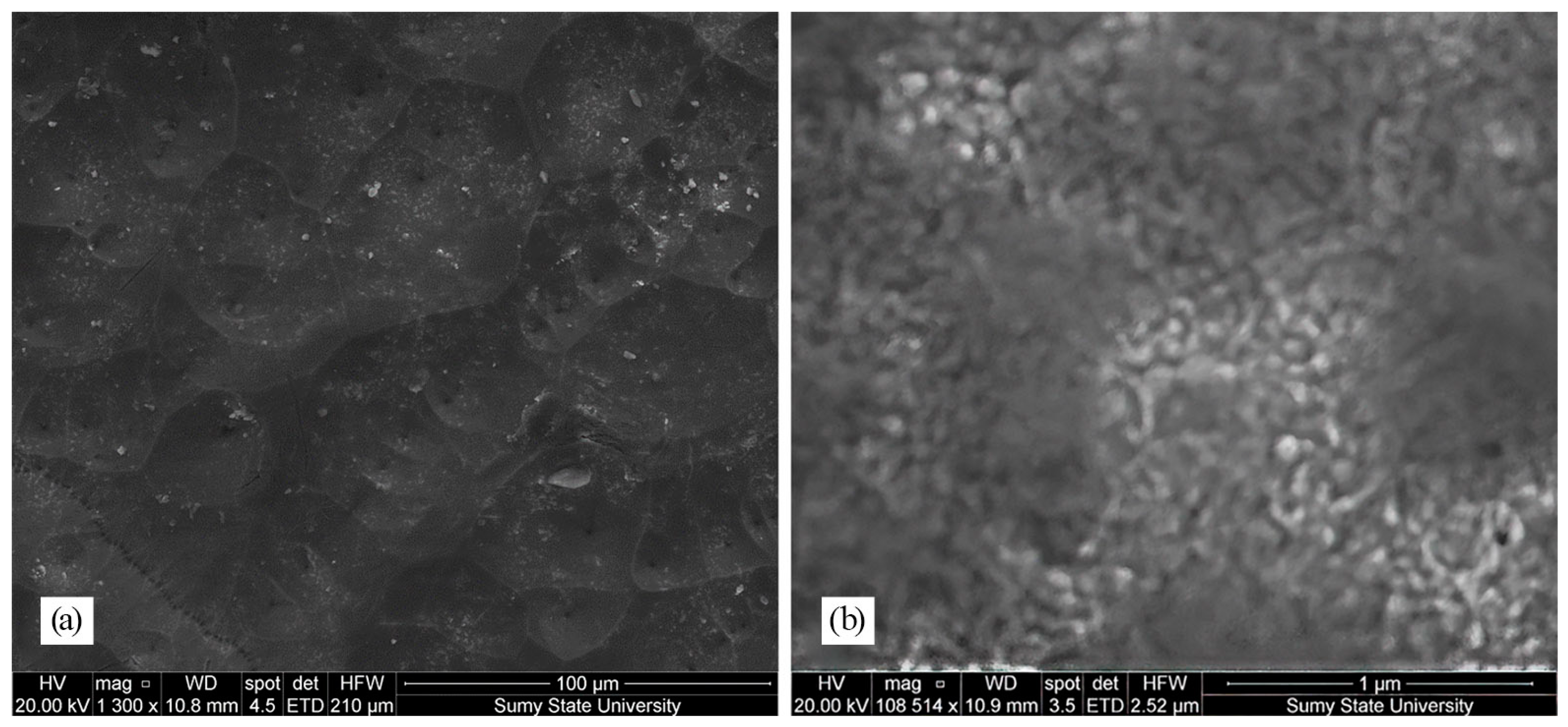
3.1. SEM Analysis
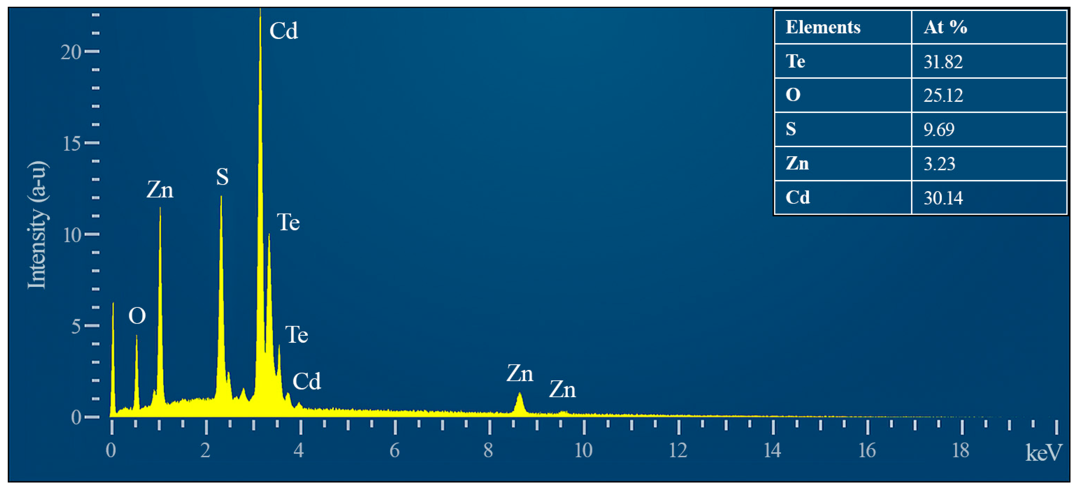
3.2. EDAX Analysis
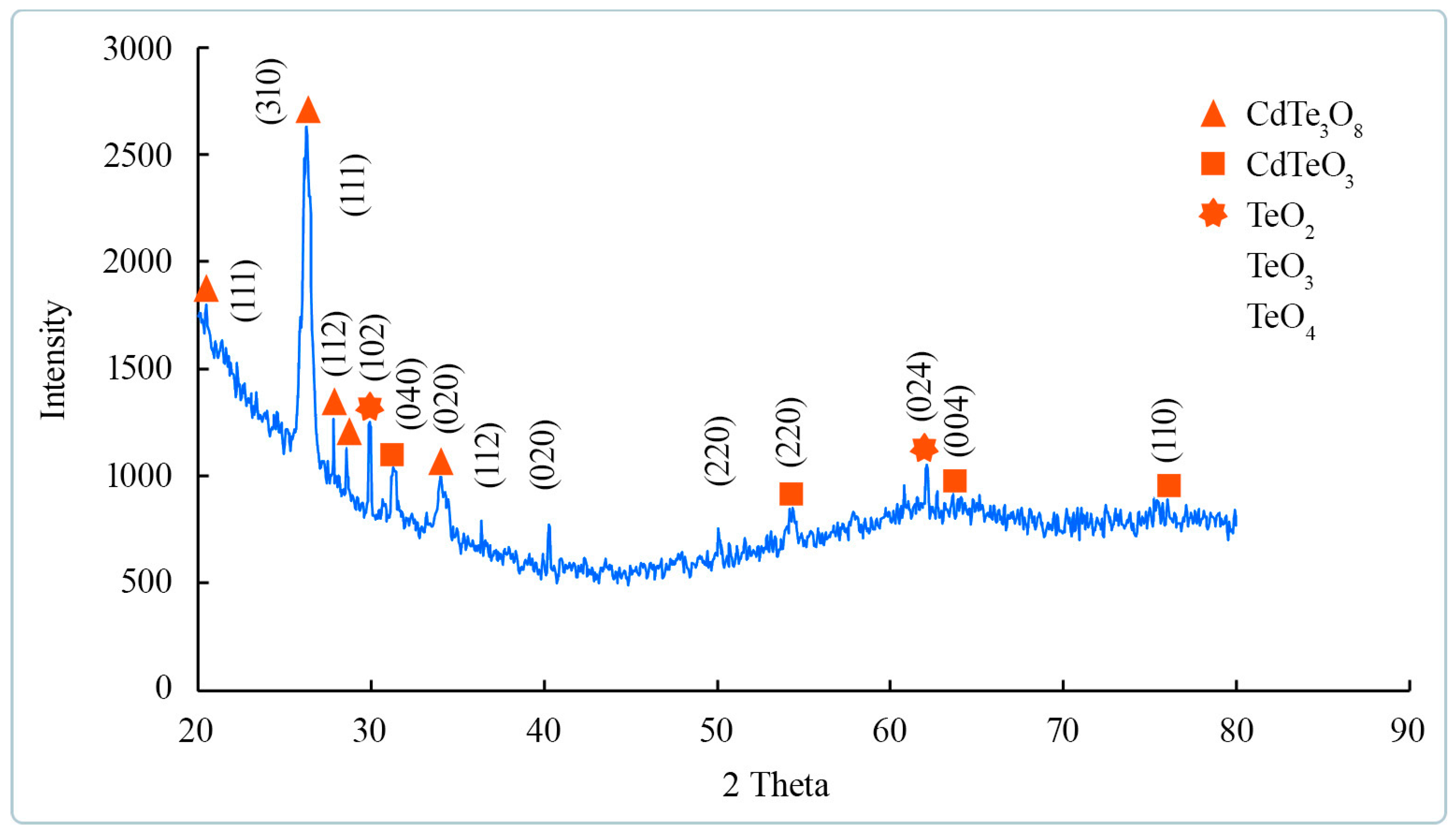
3.3. XRD Analysis
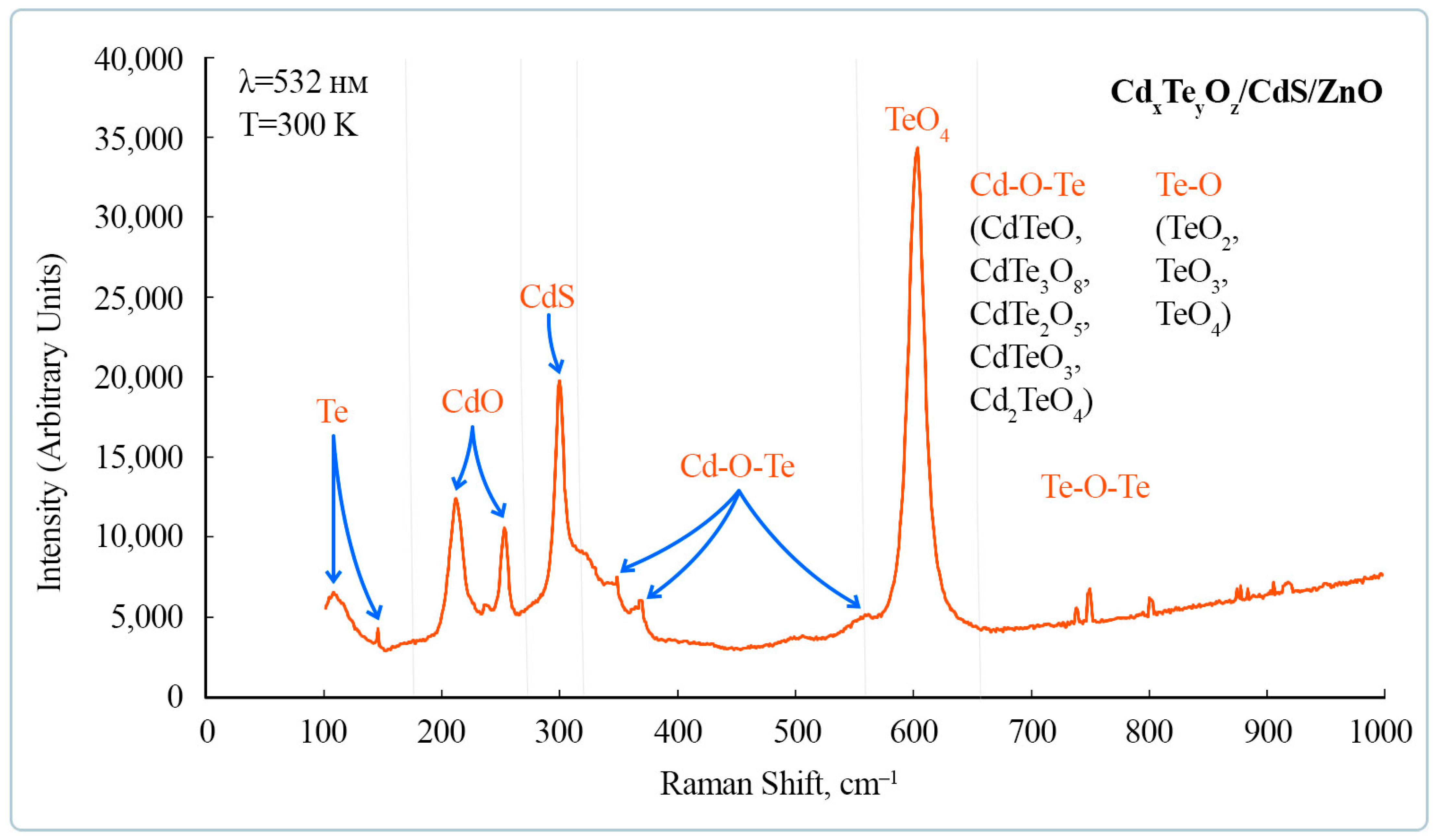
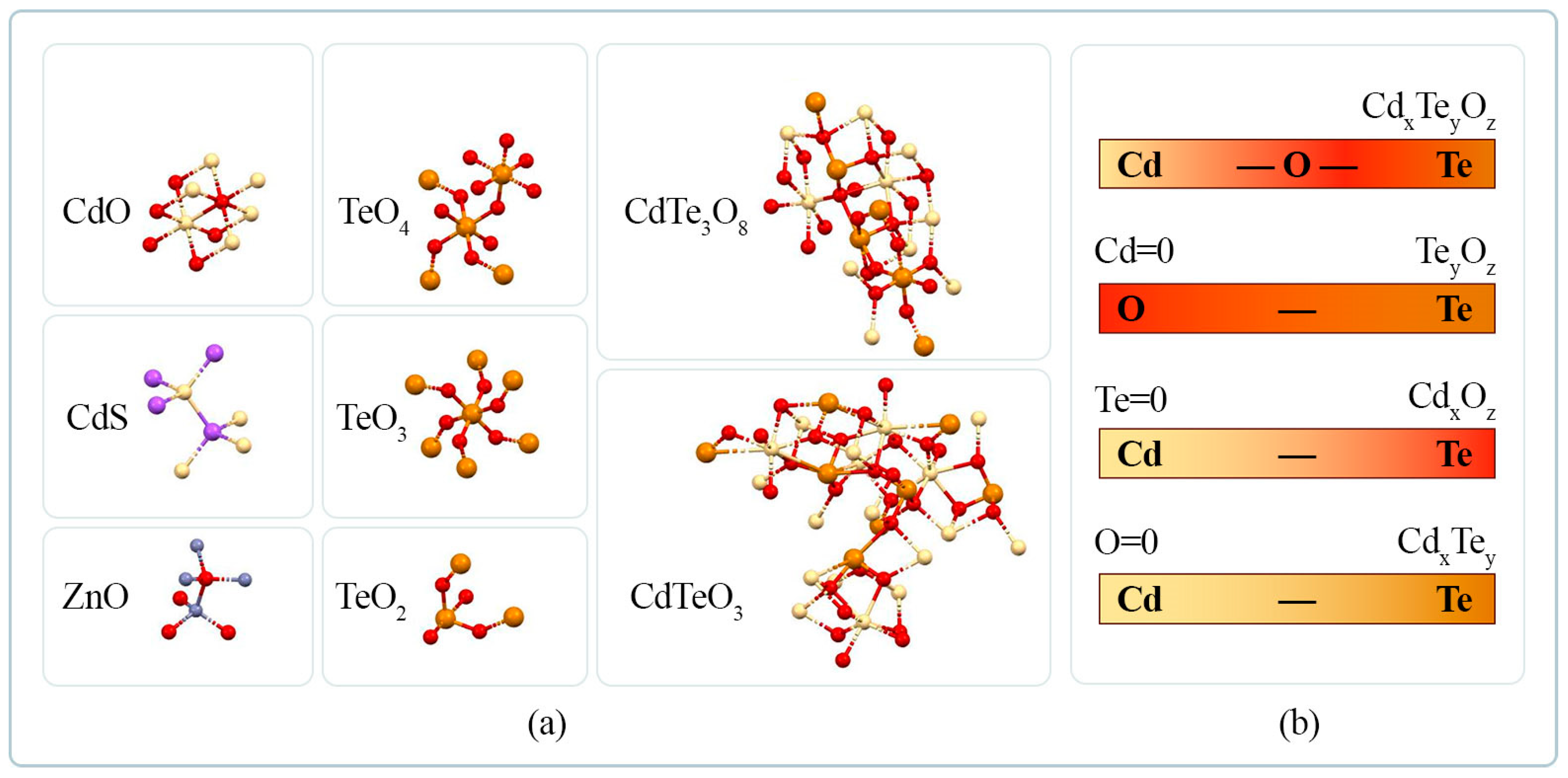
3.4. Raman Analysis
4. Discussion
5. Conclusions
Author Contributions
Funding
Institutional Review Board Statement
Informed Consent Statement
Data Availability Statement
Conflicts of Interest
References
- García de Arquer, F.P.; Talapin, D.V.; Klimov, V.I.; Arakawa, Y.; Bayer, M.; Sargent, E.H. Semiconductor quantum dots: Technological progress and future challenges. Science 2021, 373, 8541. [Google Scholar] [CrossRef] [PubMed]
- Li, M.; Chen, T.; Gooding, J.J.; Liu, J. Review of carbon and graphene quantum dots for sensing. ACS Sens. 2019, 4, 1732–1748. [Google Scholar] [CrossRef]
- Karbovnyk, I.; Savchyn, P.; Huczko, A.; Mirr, C.; Popov, A.I. FTIR studies of silicon carbide 1D- nanostructures. Mater. Sci. Forum 2015, 821–823, 261–264. [Google Scholar] [CrossRef]
- Suohikova, Y.; Vambol, S.; Vambol, V.; Mozaffari, N.; Mozaffari, N. Justification of the most rational method for the nanostructures synthesis on the semiconductors surface. J. Achiev. Mater. Manuf. Eng. 2019, 92, 19–28. [Google Scholar]
- Suchikova, Y. Provision of environmental safety through the use of porous semiconductors for solar energy sector. East.-Eur. J. Enterp. Technol. 2016, 6, 26–33. [Google Scholar] [CrossRef] [Green Version]
- Yana, S. Porous indium phosphide: Preparation and properties. In Handbook of Nanoelectrochemistry: Electrochemical Synthesis Methods, Properties, and Characterization Techniques; Springer: Berlin/Heidelberg, Germany, 2016; pp. 283–306. [Google Scholar]
- Abadias, G.; Chason, E.; Keckes, J.; Sebastiani, M.; Thompson, G.B. Stress in thin films and coatings: Current status, challenges, and prospects. J. Vac. Sci. Technol. A Vac. Surf. Films 2018, 36, 020801. [Google Scholar] [CrossRef] [Green Version]
- Chen, S.; Yuan, S.; Hou, Z.; Tang, Y.; Zhang, J.; Chen, Z. Recent progress on topological structures in ferroic thin films and heterostructures. Adv. Mater. 2021, 33, 2000857. [Google Scholar] [CrossRef]
- Suchikova, J.A.; Kidalov, V.V.; Sukach, G.A. Blueshift of photoluminescence spectrum of porous InP. ECS Trans. 2009, 25, 59–64. [Google Scholar] [CrossRef]
- Huczko, A.; Dabrowska, A.; Savchyn, V.; Popov, A.I.; Karbovnyk, I. Silicon carbide nanowires: Synthesis and cathodoluminescence. Phys. Status Solidi (B) Basic Res. 2009, 246, 2806–2808. [Google Scholar] [CrossRef]
- Pan, H.Y.; Chen, X.; Xia, X.L. A review on the evolvement of optical-frequency filtering in photonic devices in 2016–2021. Renew. Sustain. Energy Rev. 2022, 161, 112361. [Google Scholar] [CrossRef]
- Kawanishi, T. Precise optical modulation and its application to optoelectronic device measurement. Photonics 2021, 8, 160. [Google Scholar] [CrossRef]
- Yang, Q.; Dong, L.; Su, R.; Hu, B.; Wang, Z.; Dong, M. Nanostructured heterogeneous photocatalysts for hydrogen production and water splitting: A comprehensive insight. Appl. Mater. Today 2019, 17, 159–182. [Google Scholar] [CrossRef]
- Suchikova, Y.A.; Kidalov, V.V.; Sukach, G.A. Influence of the carrier concentration of indium phosphide on the porous layer formation. J. Nano- Electron. Phys. 2010, 2, 75–81. [Google Scholar]
- Vambol, S.; Vambol, V.; Suchikova, Y.; Deyneko, N. Analysis of the ways to provide ecological safety for the products of nanotechnologies throughout their life cycle. East. -Eur. J. Enterp. Technol. 2017, 1, 27–36. [Google Scholar] [CrossRef] [Green Version]
- Suchikova, Y.; Bohdanov, I.; Kovachov, S.; Popov, A.I. Texturing of indium phosphide for improving the characteristics of space solar cells. In Proceedings of the IEEE 12th International Conference on Electronics and Information Technologies, ELIT 2021—Proceedings, Lviv, Ukraine, 19–21 May 2021; pp. 194–197. [Google Scholar]
- Vambol, S.; Bogdanov, I.; Vambol, V.; Hurenko, O.; Onishchenko, S. Research into regularities of pore formation on the surface of semiconductors. East. -Eur. J. Enterp. Technol. 2017, 3, 37–44. [Google Scholar] [CrossRef] [Green Version]
- Goktas, S.; Goktas, A. A comparative study on recent progress in efficient ZnO based nanocomposite and heterojunction photocatalysts: A review. J. Alloy. Compd. 2021, 863, 158734. [Google Scholar] [CrossRef]
- Cheng, L.; Xiang, Q.; Liao, Y.; Zhang, H. CdS-based photocatalysts. Energy Environ. Sci. 2018, 11, 1362–1391. [Google Scholar] [CrossRef]
- Romeo, A.; Artegiani, E. CdTe-based thin film solar cells: Past, present and future. Energies 2021, 14, 1684. [Google Scholar] [CrossRef]
- Usseinov, A.B.; Akilbekov, A.T.; Kotomin, E.A.; Karipbayev, Z.T. The first principles calculations of CO2 adsorption on (1010) ZnO surface. AIP Conf. Proc. 2019, 2174, 020181. [Google Scholar]
- Uklein, A.V.; Multian, V.V.; Kuz’micheva, G.M.; Gayvoronsky, V.Y. Nonlinear optical response of bulk ZnO crystals with different content of intrinsic defects. Opt. Mater. 2018, 84, 738–747. [Google Scholar] [CrossRef]
- Suchikova, Y.; Lazarenko, A.; Kovachov, S.; Bardus, I.; Bohdanov, I. Formation of CdO/CdS/textured-ZnO/ZnO heterostructures by chemical deposition. Phys. Chem. Solid State 2022, 23, 361–367. [Google Scholar] [CrossRef]
- Zhilova, O.V.; Pankov, S.; Sitnikov, A.V.; Makagonov, V.A. Optical and electrical properties of thin-film heterostructures of the In2O3–ZnO system. Mater. Res. Express 2019, 6, 086330. [Google Scholar] [CrossRef]
- Chen, Y.; Xing, W.; Liu, Y.; Zhang, X.; Xu, S. Efficient and stable CdSe/CdS/ZnS quantum rods-in-matrix assembly for white LED application. Nanomaterials 2020, 10, 317. [Google Scholar] [CrossRef] [PubMed] [Green Version]
- Zhang, G.; Bai, Y.; Yu, C.; Xuan, T. Highly stable carbon nanodot-based phosphor as a color converter for WLED. J. Lumin. 2022, 246, 118836. [Google Scholar] [CrossRef]
- Wang, F.; Hou, T.; Zhao, X.; Li, Y. Ordered macroporous carbonous frameworks implanted with CdS quantum dots for efficient photocatalytic CO2 reduction. Adv. Mater. 2021, 33, 2102690. [Google Scholar] [CrossRef] [PubMed]
- Lu, K.Q.; Qi, M.Y.; Tang, Z.R.; Xu, Y.J. Earth-abundant MoS2 and cobalt phosphate dual cocatalysts on 1D CdS nanowires for boosting photocatalytic hydrogen production. Langmuir 2019, 35, 11056–11065. [Google Scholar] [CrossRef]
- Lu, H.; Liu, Y.; Zhang, S.; Wan, J.; Wang, X.; Deng, L.; Kan, J.; Wu, G. Clustered tubular S-scheme ZnO/CdS heterojunctions for enhanced photocatalytic hydrogen production. Mater. Sci. Eng. B 2023, 289, 116282. [Google Scholar] [CrossRef]
- Wang, R.; Chen, S.; Ng, Y.H.; Gao, Q.; Zhang, S. ZnO/CdS/PbS nanotube arrays with multiheterojunctions for efficient visible-light-driven photoelectrochemical hydrogen evolution. Chem. Eng. J. 2019, 362, 658–666. [Google Scholar] [CrossRef]
- Yin, X.L.; Liu, J.; Jiang, W.J.; Zhang, X.; Hu, J.S.; Wan, L.J. Urchin-like Au@ CdS/WO 3 micro/nano heterostructure as a visible-light driven photocatalyst for efficient hydrogen generation. Chem. Commun. 2015, 51, 13842–13845. [Google Scholar] [CrossRef]
- Zhu, Y.; Liu, Y.; Ai, Q.; Gao, G.; Yuan, L.; Fang, Q.; Tian, X.; Zhang, X.; Egap, E.; Ajayan, P.M.; et al. In situ synthesis of lead-free halide perovskite–COF nanocomposites as photocatalysts for photoinduced polymerization in both organic and aqueous phases. ACS Mater. Lett. 2022, 4, 464–471. [Google Scholar] [CrossRef]
- Khrypunov, G.; Vambol, S.; Deyneko, N.; Suchikova, Y. Increasing the efficiency of film solar cells based on cadmium telluride. East. -Eur. J. Enterp. Technol. 2016, 6, 12–18. [Google Scholar] [CrossRef] [Green Version]
- Usseinov, A.; Koishybayeva, Z.; Platonenko, A.; Popov, A.I. Vacancy defects in Ga2O3: First-principles calculations of electronic structure. Materials 2021, 14, 7384. [Google Scholar] [CrossRef] [PubMed]
- Usseinov, A.; Koishybayeva, Z.; Platonenko, A.; Popov, A.I. Ab-Initio Calculations of Oxygen Vacancy in Ga2O3Crystals. Latv. J. Phys. Tech. Sci. 2021, 58, 3–10. [Google Scholar]
- Luchechko, A.; Vasyltsiv, V.; Kostyk, L.; Tsvetkova, O.; Popov, A.I. Shallow and deep trap levels in X-ray irradiated β-Ga2O3: Mg. Nucl. Instrum. Methods Phys. Res. Sect. B: Beam Interact. Mater. At. 2019, 441, 12–17. [Google Scholar] [CrossRef]
- Suchikova, Y.; Bohdanov, I.; Kovachov, S.; Popov, A.I. The Synthesis of porous indium phosphide with nickel oxide crystallites on the surface. J. Electrochem. Sci. Eng. 2022, 12, 593–601. [Google Scholar] [CrossRef]
- Suchikova, Y.O.; Bogdanov, I.T.; Kovachov, S.S. Oxide crystals on the surface of porous indium phosphide. Arch. Mater. Sci. Eng. 2019, 98, 49–56. [Google Scholar] [CrossRef]
- Suchikova, Y.; Lazarenko, A.; Kovachov, S.; Popov, A.I. Formation of porous Ga2O3/GaAs layers for electronic devices. In Proceedings of the 16th International Conference on Advanced Trends in Radioelectronics, Telecommunications and Computer Engineering, TCSET, Lviv-Slavske, Ukraine, 22–26 February 2022; pp. 410–413. [Google Scholar]
- Muftah, G.E.A.; Hassan, M.; Dharmadasa, I.M. Electrodeposited CdTe Thin Film Solar Cells: Chloride Treatment and Improved Efficiency. Int. J. Eng. Innov. Res. 2018, 7, 2277–5668. [Google Scholar]
- Balakhayeva, R.; Akilbekov, A.; Baimukhanov, Z.; Popov, A.I.; Dauletbekova, A. CdTe Nanocrystal Synthesis in SiO2/Si Ion-Track Template: The Study of Electronic and Structural Properties. Phys. Status Solidi (A) Appl. Mater. Sci. 2021, 218, 2000231. [Google Scholar] [CrossRef]
- Akilbekov, A.; Balakhayeva, R.; Zdorovets, M.; Popov, A.I.; Dauletbekova, A. Ion track template technology for fabrication of CdTe and CdO nanocrystals. Nucl. Instrum. Methods Phys. Res. Sect. B: Beam Interact. Mater. At. 2020, 481, 30–34. [Google Scholar] [CrossRef]
- Krämer, V.; Brandt, G. Structure of cadmium tellurate (IV), CdTeO3. Acta Crystallogr. Sect. C: Cryst. Struct. Commun. 1985, 41, 1152–1154. [Google Scholar] [CrossRef]
- Menéndez-Proupin, E.; Gutiérrez, G.; Palmero, E.; Peña, J.L. Electronic structure of crystalline binary and ternary Cd− Te− O compounds. Phys. Rev. B 2004, 70, 035112. [Google Scholar] [CrossRef] [Green Version]
- Heiba, Z.K. X-ray structural phase analysis of CdTe semiconductor annealed in air. Cryst. Res. Technol. J. Exp. Ind. Crystallogr. 2003, 38, 488–493. [Google Scholar] [CrossRef]
- Durose, K.; Boyle, D.; Abken, A.; Ottley, C.J.; Nollet, P.; Degrave, S.; Bonnet, D. Key aspects of CdTe/CdS solar cells. Phys. Status Solidi (B) 2002, 229, 1055–1064. [Google Scholar] [CrossRef]
- Jiménez-Sandoval, S.; Garnett-Ruiz, G.E.; Santos-Cruz, J.; Jiménez-Sandoval, O.; Torres-Delgado, G.; Castanedo-Pérez, R.; Morales-Sanchez, E. Band gap tuning and high electrical conductivity in amorphous and polycrystalline films of the Cux(CdTe)yOz system. J. Appl. Phys. 2006, 100, 113713. [Google Scholar] [CrossRef]
- Ramírez-Bon, R.; Espinoza-Beltrán, F.J.; Arizpe-Chávez, H.; Zelaya-Angel, O.; Sánchez-Sinencio, F. Structural and optical studies in a-CdTe: O annealed films. J. Appl. Phys. 1996, 79, 7682–7687. [Google Scholar] [CrossRef]
- El Azhari, M.Y.; Azizan, M.; Bennouna, A.; Outzourhit, A.; Ameziane, E.L.; Brunel, M. Optical properties of oxygenated amorphous cadmium telluride thin films. Sol. Energy Mater. Sol. Cells 1997, 45, 341–352. [Google Scholar] [CrossRef]
- Bartolo-Pérez, P.; Castro-Rodrıguez, R.; Caballero-Briones, F.; Cauich, W.; Peña, J.L.; Farias, M.H. X-Ray photoelectron spectroscopy study of CdTe oxide films grown by rf sputtering with an Ar–NH3 plasma. Surf. Coat. Technol. 2002, 155, 16–20. [Google Scholar] [CrossRef]
- Hussain, O.M.; Reddy, P.J. Characterization of thin film n-CdS/p-CdTe heterojunctions. Vacuum 1991, 42, 657–659. [Google Scholar] [CrossRef]
- El Azhari, M.Y.; Azizan, M.; Bennouna, A.; Outzourhit, A.; Ameziane, E.L.; Brunel, M. Preparation and characterization of CdTeO3 thin films. Thin Solid Films 2000, 366, 82–87. [Google Scholar] [CrossRef]
- Kovachov, S.; Bohdanov, I.; Karipbayev, Z.; Suchikova, Y.; Tsebriienko, T.; Popov, A.I. Layer-by-Layer Synthesis and Analysis of the the Phase Composition of CdxTeyOz/CdS/por-ZnO/ZnO Heterostructure. In Proceedings of the IEEE 3rd KhPI Week on Advanced Technology (KhPIWeek), Kharkiv, Ukraine, 3–7 October 2022; pp. 1–6. [Google Scholar]
- Guillén-Cervantes, A.; Becerril-Silva, M.; Silva-López, H.E.; Arias-Cerón, J.S.; Campos-González, E.; Pérez-González, M.; Zelaya-Ángel, O. Structural and optical properties of CdTe+ CdTeO 3 nanocomposite films with broad blueish photoluminescence. J. Mater. Sci. Mater. Electron. 2020, 31, 7133–7140. [Google Scholar] [CrossRef]
- Oh, K.; Han, M.; Kim, K.; Heo, Y.; Moon, C.; Park, S.; Nam, S. Development and evaluation of polycrystalline cadmium telluride dosimeters for accurate quality assurance in radiation therapy. J. Instrum. 2016, 11, C02040. [Google Scholar] [CrossRef]
- Hussin, R.; Leong, N.S.; Alias, N.S. Structural investigation of crystalline host phosphor cadmium tellurite systems. Malays. J. Fundam. Appl. Sci. 2009, 5, 17–27. [Google Scholar] [CrossRef] [Green Version]
- Devi, R.A.; Latha, M.; Velumani, S.; Oza, G.; Reyes-Figueroa, P.; Rohini, M.; Becerril-Juarez, I.G.; Lee, J.-H.; Yi, J. Synthesis and characterization of cadmium sulfide nanoparticles by chemical precipitation method. J. Nanosci. Nanotechnol. 2015, 15, 8434–8439. [Google Scholar] [CrossRef] [PubMed]
- Najm, A.S.; Naeem, H.S.; Alwarid, D.A.R.M.; Aljuhani, A.; Hasbullah, S.A.; Hasan, H.A.; Sopian, K.; Bais, B.; Al-Iessa, H.J.; Majdi, H.S.; et al. Mechanism of Chemical Bath Deposition of CdS Thin Films: Influence of Sulphur Precursor Concentration on Microstructural and Optoelectronic Characterizations. Coatings 2022, 12, 1400. [Google Scholar] [CrossRef]
- Wu, Y.; Yang, X.; Chen, H.; Zhang, K.; Qin, C.; Liu, J.; Peng, W.; Islam, A.; Bi, E.; Ye, F.; et al. Highly compact TiO2 layer for efficient hole-blocking in perovskite solar cells. Appl. Phys. Express 2014, 7, 052301. [Google Scholar] [CrossRef]
- Yang, G.; Tao, H.; Qin, P.; Ke, W.; Fang, G. Recent progress in electron selective layers for efficient perovskite solar cells. J. Mater. Chem. A 2016, 4, 3970–3990. [Google Scholar] [CrossRef]
- Masood, M.T.; Qudsia, S.; Hadadian, M.; Weinberger, C.; Nyman, M.; Ahläng, C.; Dahlström, S.; Liu, M.; Vivo, P.; Österbacka, R.; et al. Investigation of Well-Defined Pinholes in TiO2 Electron Selective Layers Used in Planar Heterojunction Perovskite Solar Cells. Nanomaterials 2020, 10, 181. [Google Scholar] [CrossRef] [Green Version]
- Zhao, C.; Zou, X.; He, S. CdTeO3 deposited mesoporous NiO photocathode for a solar cell. J. Nanomater. 2014, 2014, 372381. [Google Scholar] [CrossRef] [Green Version]
- Caballero-Briones, F.; Peña, J.L.; Martel, A.; Iribarren, A.; Zapata-Navarro, A. Structural analysis of Cd–Te–O films prepared by RF reactive sputtering. J. Noncryst. Solids 2008, 354, 3756–3761. [Google Scholar] [CrossRef]
- Caballero-Briones, F.; Zapata-Navarro, A.; Martel, A.; Iribarren, A.; Peña, J.L.; Jiménez-Sandoval, S. Compositional mixture in RF sputtered CdTe oxide films. Raman spectroscopy results. Superf. Vacio 2003, 16, 38–42. [Google Scholar]
- Carmona-Rodríguez, J.; Lozada-Morales, R.; Jiménez-Sandoval, O.; Rodríguez-Melgarejo, F.; Meléndez-Lira, M.; Jiménez-Sandoval, S.J. CdTeOx to CdTeO3 structural phase transition in as-grown polycrystalline films by reactive sputtering. J. Appl. Phys. 2008, 103, 123516. [Google Scholar] [CrossRef]
- Wu, L.; Li, Z.; Wang, D.; Lei, X.; Cai, Y.; Wang, D. CdTe surface passivation by electric field induced at the metal-oxide/CdTe interface. Solar Energy 2021, 225, 83–90. [Google Scholar] [CrossRef]
- Erken, O. Effect of cycle numbers on the structural, linear and nonlinear optical properties in Fe2O3 thin films deposited by SILAR method. Curr. Appl. Phys. 2022, 34, 7–18. [Google Scholar] [CrossRef]
- Sathya, M.; Selvan, G.; Karunakaran, M.; Kasirajan, K.; Usha, S.; Logitha, M.; Baskaran, P. Synthesis and characterization of cadmium doped on ZnO thin films prepared by SILAR method for photocatalytic degradation properties of MB under UV irradiation. Eur. Phys. J. Plus 2023, 138, 67. [Google Scholar] [CrossRef]
- Lindroos, S.; Arnold, A.; Leskelä, M. Growth of CuS thin films by the successive ionic layer adsorption and reaction method. Appl. Surf. Sci. 2000, 158, 75–80. [Google Scholar] [CrossRef]
- Menéndez-Proupin, E.; Giannozzi, P.; Peralta, J.; Gutiérrez, G. Ab initio molecular dynamics study of amorphous CdTeOx alloys: Structural properties. Phys. Rev. B 2009, 79, 014205. [Google Scholar] [CrossRef] [Green Version]
- Weil, M. New phases in the Ca–Te–O and Cd–Te–O systems: Calcium tellurite (IV) Ca4Te5O14 and the cadmium compounds Cd2Te3O9 and Cd2Te2O7 with mixed-valent oxotellurium (IV/VI) anions. Solid-State Sci. 2004, 6, 29–37. [Google Scholar] [CrossRef]
- Menéndez-Proupin, E.; Gutiérrez, G.; Palmero, E.; Peña, J.L. Electronic structure of binary and ternary components of CdTe:O thin films. Phys. Status Solidi (C) 2004, 1, S104–S107. [Google Scholar] [CrossRef]


| Stage № | Name, Purpose | Solution | Duration |
|---|---|---|---|
| 1 | Formation of CdS/ZnO structure | CdCl2:CH4N2S:NH3 = 0.1 M:0.1 M:5 M | 5 h |
| 2 | Rinsing 1, removal of excess reaction products | Distilled H2O | 2 min |
| 3 | Formation of CdxTeyOz/CdS/ZnO heterostructure | Aqueous solution 0.01 M Na2TeO3 | 10 min |
| 4 | Rinsing 3, removal of excess reaction products | H2O2 | 2 min |
| 5 | Formation of CdxTeyOz/CdS/ZnO heterostructure | Alcohol solution 0.01 M Cd(NO3)2 | 10 min |
| 6 | Rinsing 3, removal of excess reaction products | H2O2 | 2 min |
| Characteristic | ZnO | CdS | CdTe | CdO | TeO2 | TeO3 | TeO4 | CdTeO3 | CdTe3O8 |
|---|---|---|---|---|---|---|---|---|---|
| COD number | 1,011,258 | 1,011,054 | - | 1,011,003 | 9,008,125 | 7,035,629 | - | 7,041,644 | - |
| Crystal system | Hexagonal | Hexagonal | Hexagonal | Cubic | Orthorhombic | Trigonal | Monoclinic | Orthorhombic | Monoclinic |
| Space group | P63-mc | P63mc | P63mc | Fm-3 m | Pbca | R-3c | P2/c | Pnma | P2/c |
| Space group number | 186 | 186 | 186 | 225 | 61 | 167 | 14 | 62 | 13 |
| Volume of cell, Å−3 | 46.692 | 104.86 | 145.82 | 103.76 | 395.35 | 97.26 | 136.77 | 1196.38 | 771.50 |
| a, Å | 3.220 | 4.207 | 4.684 | 4.699 | 5.6 | 5.285 | 4.96 | 7.458 | 14.066 |
| b, Å | 3.220 | 4.207 | 4.684 | 4.699 | 5.75 | 5.285 | 5.23 | 14.522 | 5.872 |
| c, Å | 5.220 | 6.843 | 7.674 | 4.699 | 12.3 | 5.285 | 5.77 | 11.046 | 10.521 |
| α, o | 90 | 90 | 90 | 90 | 90 | 57.051 | 65.83 | 90 | 90 |
| β, o | 90 | 90 | 90 | 90 | 90 | 57.051 | 90 | 90 | 117.4 |
| γ, o | 120 | 120 | 120 | 90 | 90 | 57.051 | 90 | 90 | 90 |
Disclaimer/Publisher’s Note: The statements, opinions and data contained in all publications are solely those of the individual author(s) and contributor(s) and not of MDPI and/or the editor(s). MDPI and/or the editor(s) disclaim responsibility for any injury to people or property resulting from any ideas, methods, instructions or products referred to in the content. |
© 2023 by the authors. Licensee MDPI, Basel, Switzerland. This article is an open access article distributed under the terms and conditions of the Creative Commons Attribution (CC BY) license (https://creativecommons.org/licenses/by/4.0/).
Share and Cite
Suchikova, Y.; Kovachov, S.; Bohdanov, I.; Popova, E.; Moskina, A.; Popov, A. Characterization of CdxTeyOz/CdS/ZnO Heterostructures Synthesized by the SILAR Method. Coatings 2023, 13, 639. https://doi.org/10.3390/coatings13030639
Suchikova Y, Kovachov S, Bohdanov I, Popova E, Moskina A, Popov A. Characterization of CdxTeyOz/CdS/ZnO Heterostructures Synthesized by the SILAR Method. Coatings. 2023; 13(3):639. https://doi.org/10.3390/coatings13030639
Chicago/Turabian StyleSuchikova, Yana, Sergii Kovachov, Ihor Bohdanov, Elena Popova, Aleksandra Moskina, and Anatoli Popov. 2023. "Characterization of CdxTeyOz/CdS/ZnO Heterostructures Synthesized by the SILAR Method" Coatings 13, no. 3: 639. https://doi.org/10.3390/coatings13030639