
Al2O3 Ultra-Thin Films Deposited by PEALD for Rubidium Optically Pumped Atomic Magnetometers with On-Chip Photodiode

Abstract
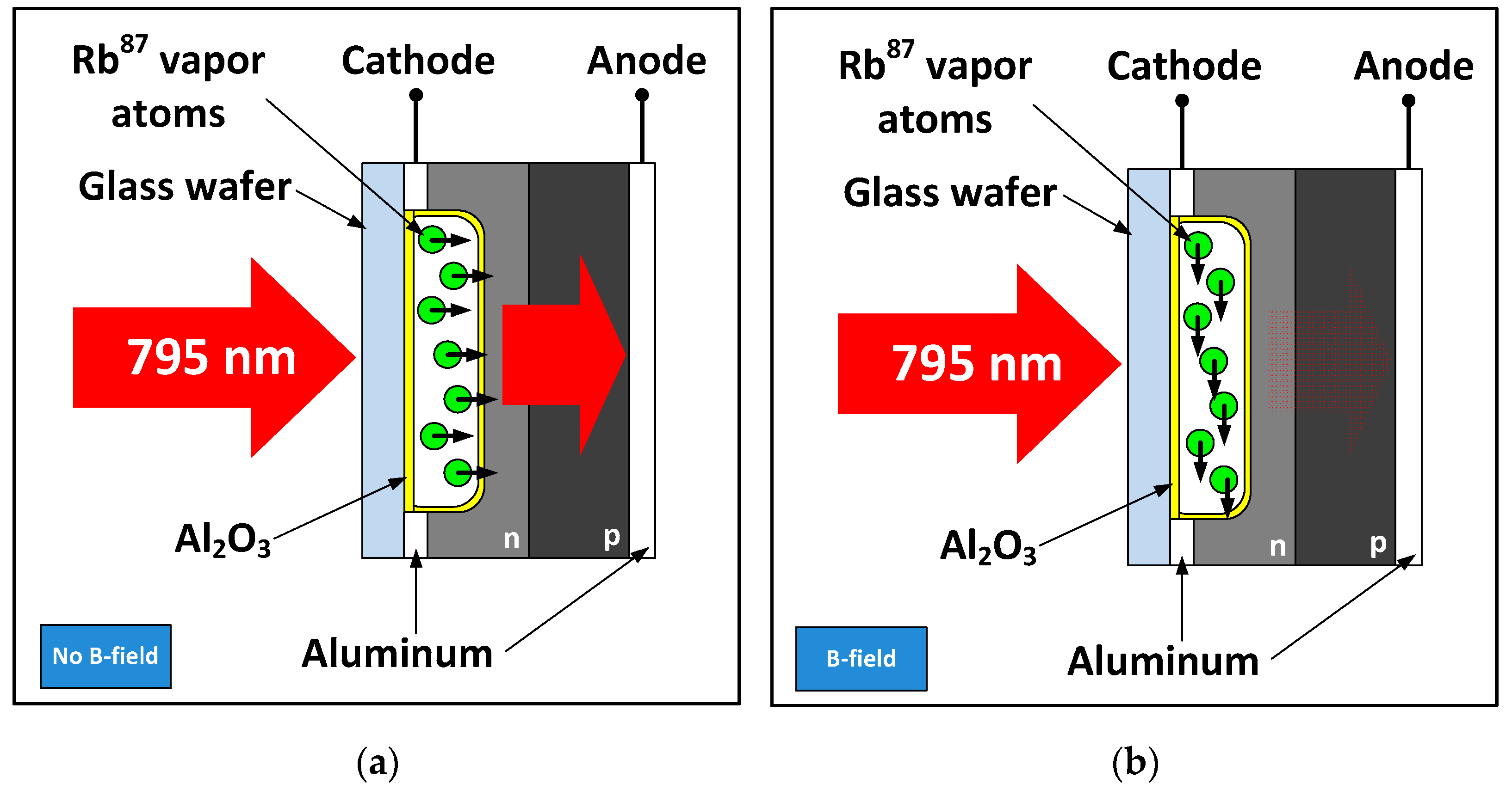
:1. Introduction
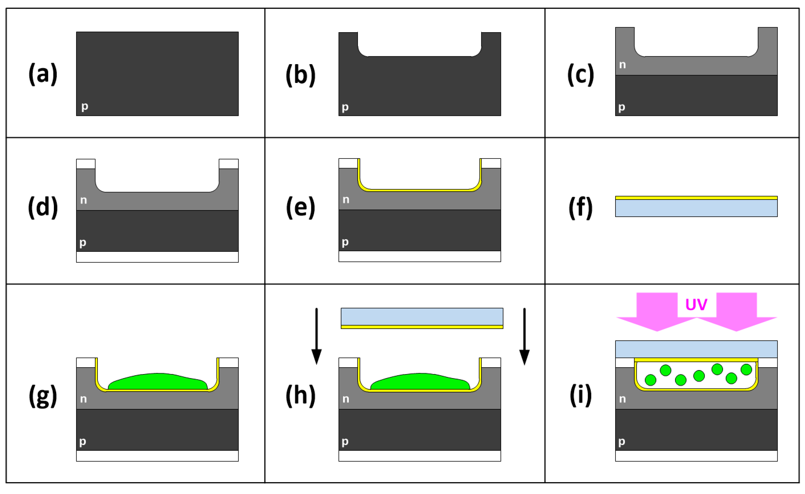
2. Materials and Methods
3. Results and Discussion
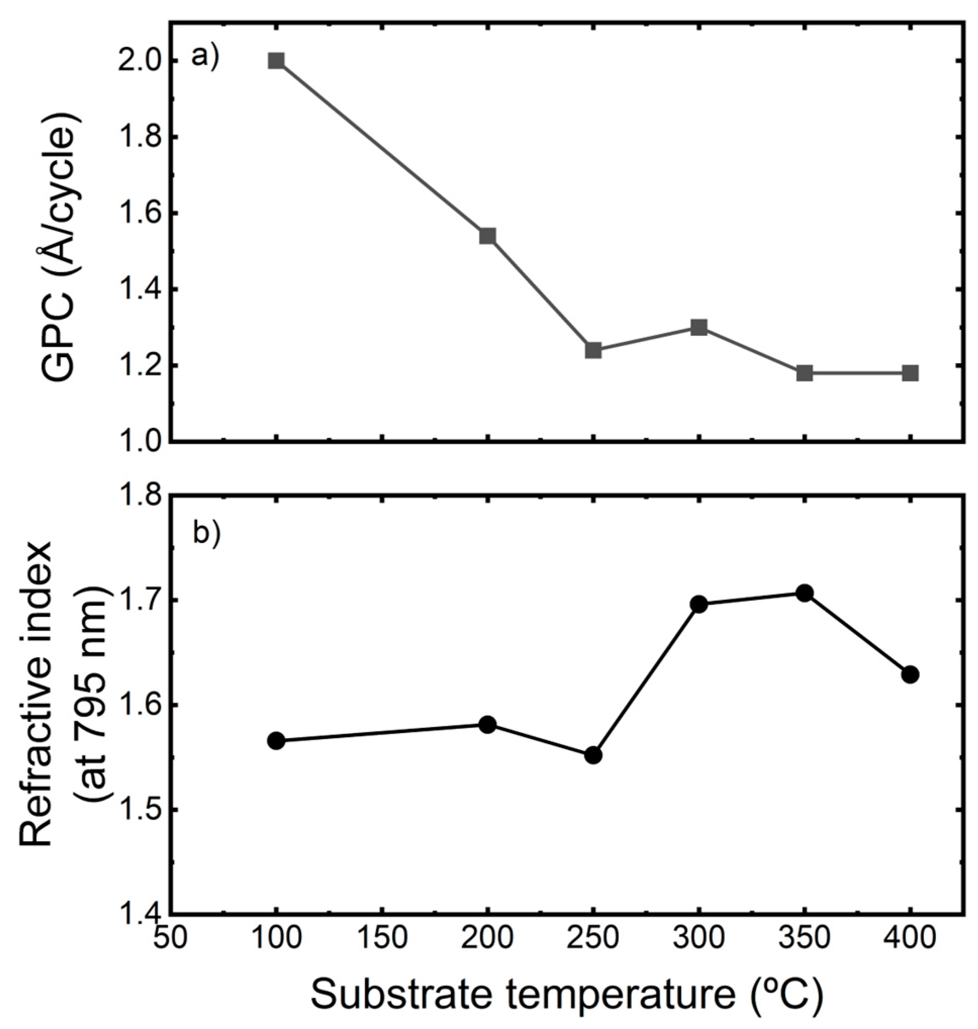
3.1. Optical Characterization
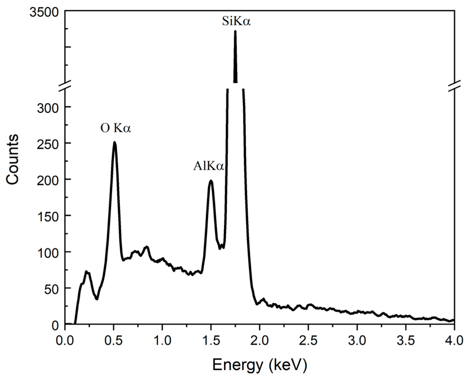
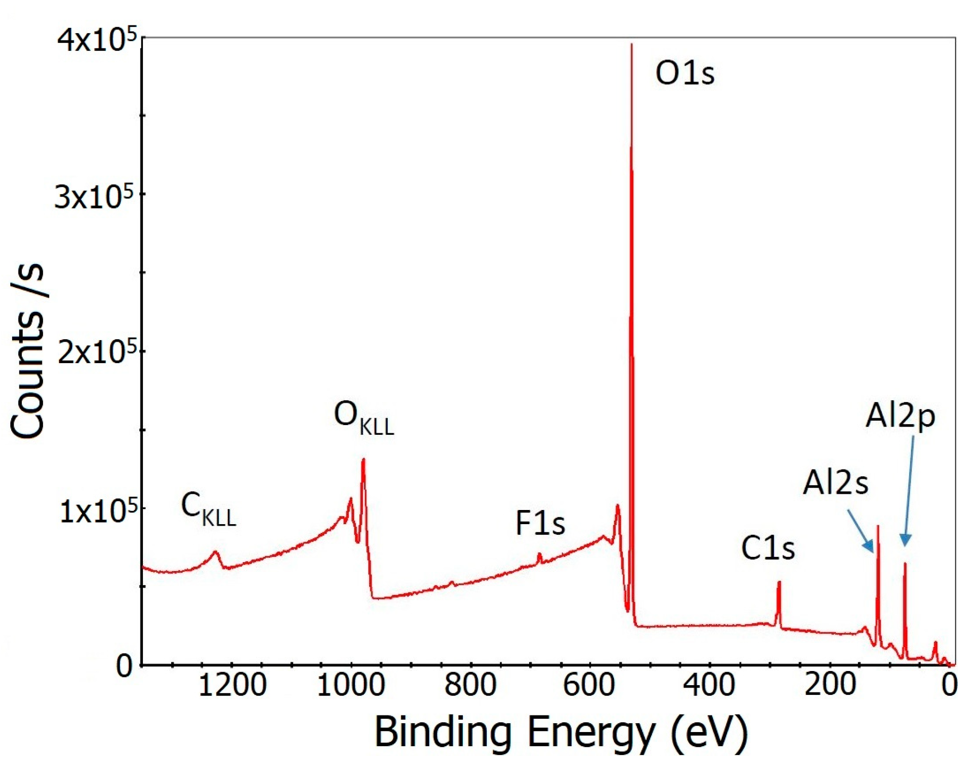
3.2. Chemical Characterization
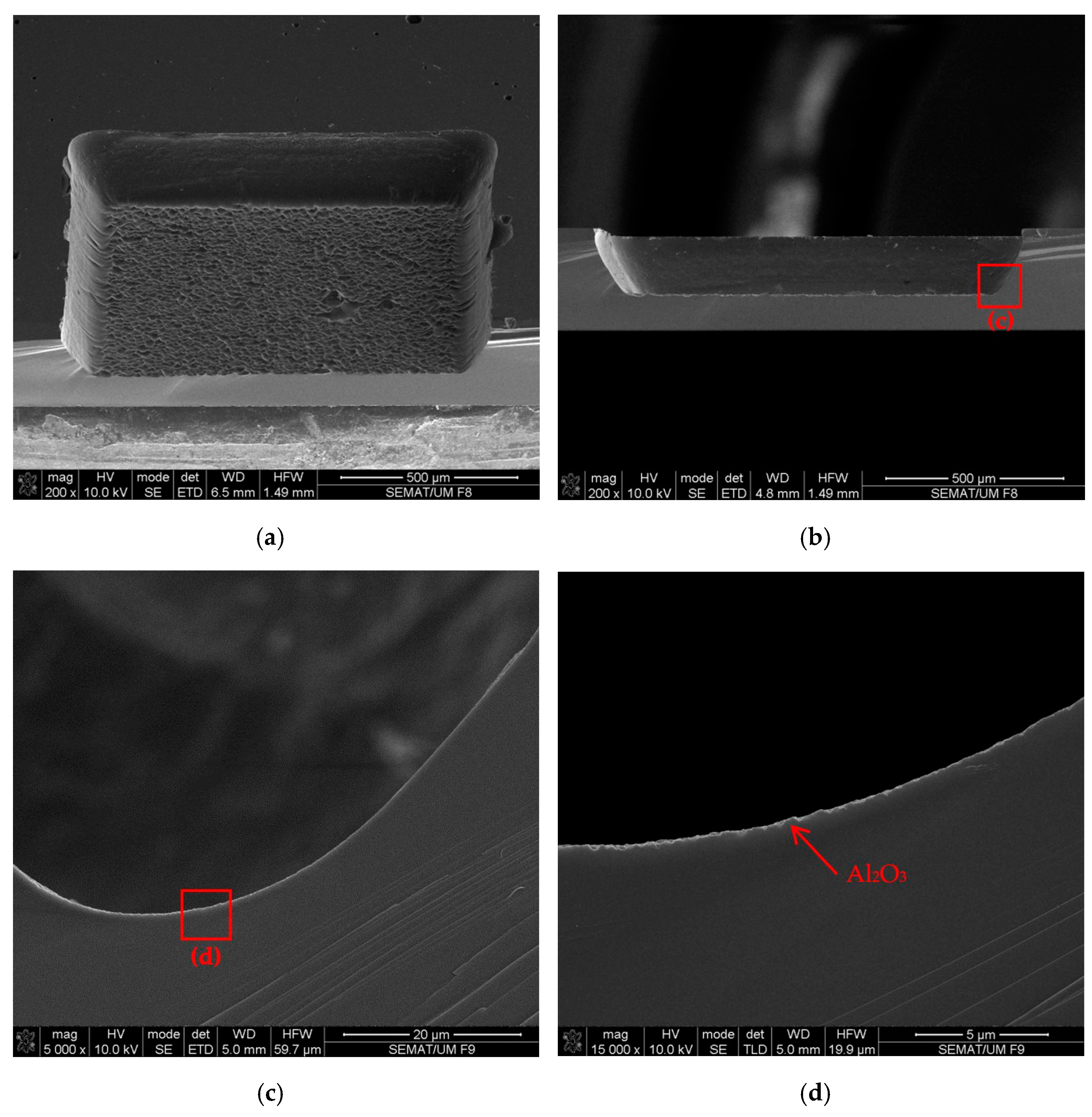
3.3. Topographic Characterization
3.4. Crystalline Property, Adhesion and Surface Wettability
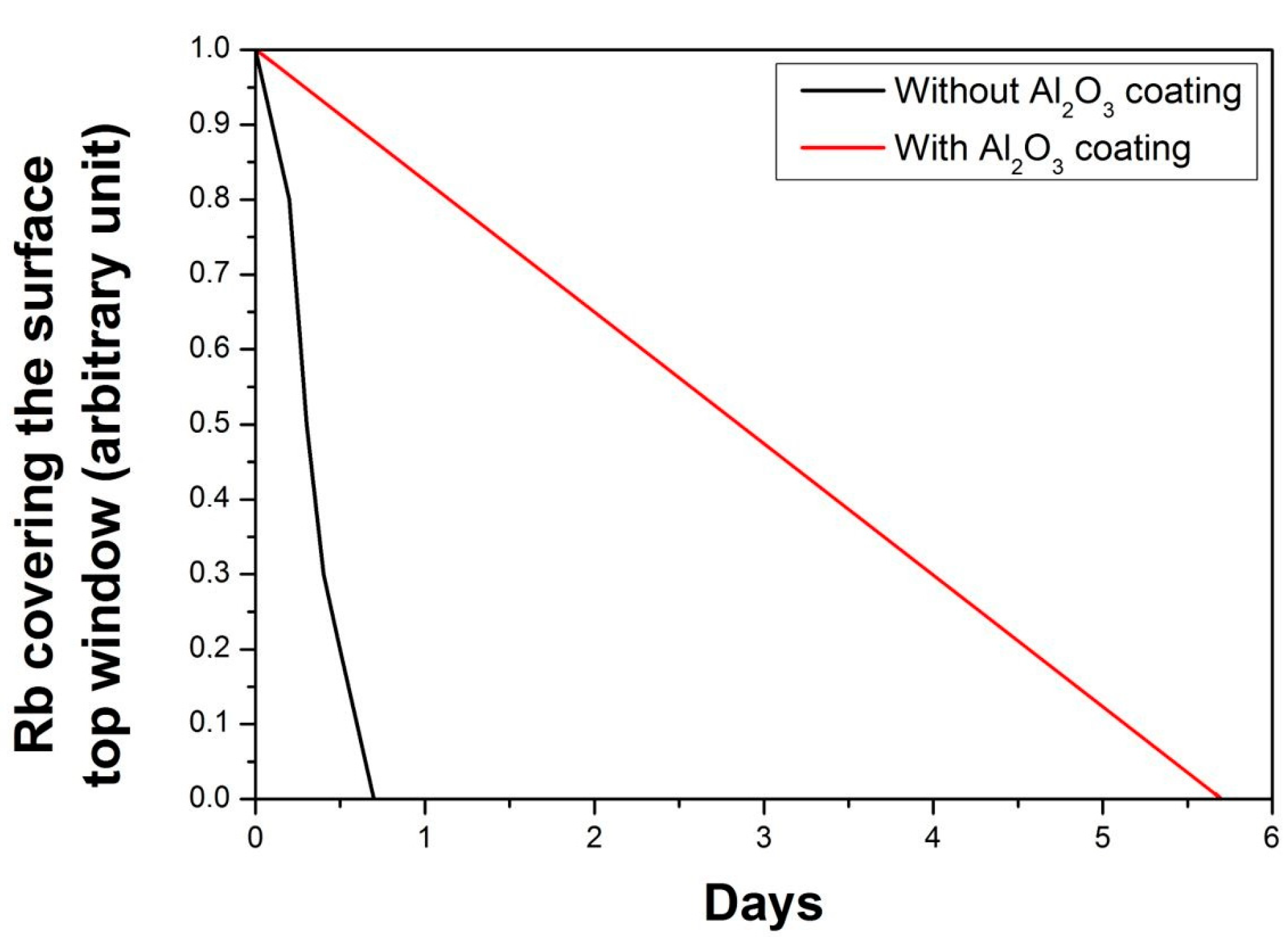
3.5. Measurement of the Rubidium Consumption
4. Conclusions
Author Contributions
Funding
Institutional Review Board Statement
Informed Consent Statement
Data Availability Statement
Conflicts of Interest
References
- Tierney, T.M.; Holmes, N.; Mellor, S.; López, J.D.; Roberts, G.; Hill, R.M.; Boto, E.; Leggett, J.; Shah, V.; Brookes, M.J.; et al. Optically Pumped Magnetometers: From Quantum Origins to Multi-Channel Magnetoencephalography. Neuroimage 2019, 199, 598–608. [Google Scholar] [CrossRef] [PubMed]
- Pétremand, Y.; Affolderbach, C.; Straessle, R.; Pellaton, M.; Briand, D.; Mileti, G.; De Rooij, N.F. Microfabricated Rubidium Vapour Cell with a Thick Glass Core for Small-Scale Atomic Clock Applications. J. Micromech. Microeng. 2012, 22, 025013. [Google Scholar] [CrossRef] [Green Version]
- Shah, V.K.; Wakai, R.T. A Compact, High Performance Atomic Magnetometer for Biomedical Applications. Phys. Med. Biol. 2013, 58, 8153–8161. [Google Scholar] [CrossRef] [Green Version]
- Woetzel, S.; Talkenberg, F.; Scholtes, T.; Ijsselsteijn, R.; Schultze, V.; Meyer, H.G. Lifetime Improvement of Micro-Fabricated Alkali Vapor Cells by Atomic Layer Deposited Wall Coatings. Surf. Coat. Technol. 2013, 221, 158–162. [Google Scholar] [CrossRef]
- Karlen, S.; Gobet, J.; Overstolz, T.; Haesler, J.; Lecomte, S. Lifetime Assessment of RbN3-Filled MEMS Atomic Vapor Cells with Al2O3 Coating. Opt. Express 2017, 25, 2187. [Google Scholar] [CrossRef] [PubMed]
- Castillo-Saenz, J.; Nedev, N.; Valdez-Salas, B.; Curiel-Alvarez, M.; Mendivil-Palma, M.I.; Hernandez-Como, N.; Martinez-Puente, M.; Mateos, D.; Perez-Landeros, O.; Martinez-Guerra, E. Properties of Al2O3 Thin Films Grown by PE-ALD at Low Temperature Using H2O and O2 Plasma Oxidants. Coatings 2021, 11, 1266. [Google Scholar] [CrossRef]
- Naumann, F.; Reck, J.; Gargouri, H.; Gruska, B.; Blümich, A.; Mahmoodinezhad, A.; Janowitz, C.; Henkel, K.; Flege, J.I. In Situ Real-Time and Ex Situ Spectroscopic Analysis of Al2O3 Films Prepared by Plasma Enhanced Atomic Layer Deposition. J. Vac. Sci. Technol. B 2020, 38, 014014. [Google Scholar] [CrossRef]
- Dingemans, G.; Van De Sanden, M.C.M.; Kessels, W.M.M. Influence of the Deposition Temperature on the C-Si Surface Passivation by Al2O3 Films Synthesized by ALD and PECVD. Electrochem. Solid-State Lett. 2010, 13, 76–79. [Google Scholar] [CrossRef] [Green Version]
- Van Hemmen, J.L.; Heil, S.B.S.; Klootwijk, J.H.; Roozeboom, F.; Hodson, C.J.; Van de Sanden, M.C.M.; Kessels, W.M.M. Plasma and Thermal ALD of Al2O3 in a Commercial 200 mm ALD Reactor. J. Electrochem. Soc. 2007, 154, G165. [Google Scholar] [CrossRef] [Green Version]
- Ding, J.N.; Wang, X.F.; Yuan, N.Y.; Li, C.L.; Zhu, Y.Y.; Kan, B. The influence of substrate on the adhesion behaviors of atomic layer deposited aluminum oxide films. Surf. Coat. Technol. 2011, 205, 2846–2851. [Google Scholar] [CrossRef]
- Jakschik, S.; Schroeder, U.; Hecht, T.; Gutsche, M.; Seidl, H.; Bartha, J.W. Crystallization behavior of thin ALD-Al2O3 films. Thin Solid Film. 2003, 425, 216–220. [Google Scholar] [CrossRef]
- Li, H.Y.; Liu, Y.F.; Duan, Y.; Yang, Y.Q.; Lu, Y.N. Method for Aluminum Oxide Thin Films Prepared through Low Temperature Atomic Layer Deposition for Encapsulating Organic Electroluminescent Devices. Materials 2015, 8, 600–610. [Google Scholar] [CrossRef] [Green Version]
- George, S.M. Atomic Layer Deposition: An Overview. Chem. Rev. 2010, 110, 111–131. [Google Scholar] [CrossRef]
- Groner, M.D.; Fabreguette, F.H.; Elam, J.W.; George, S.M. Low-Temperature Al2O3 Atomic Layer Deposition. Chem. Mater. 2004, 16, 639–645. [Google Scholar] [CrossRef]
- Groner, M.D.; Elam, J.W.; Fabreguette, F.H.; George, S.M. Electrical Characterization of Thin Al2O3 Films Grown by Atomic Layer Deposition on Silicon and Various Metal Substrates. Thin Solid Film. 2002, 413, 186–197. [Google Scholar] [CrossRef]
- Wilson, C.A.; Grubbs, R.K.; George, S.M. Nucleation and Growth during Al2O3 Atomic Layer Deposition on Polymers. Chem. Mater. 2005, 17, 5625–5634. [Google Scholar] [CrossRef]
- Marichy, C.; Bechelany, M.; Pinna, N. Atomic Layer Deposition of Nanostructured Materials for Energy and Environmental Applications. Adv. Mater. 2012, 24, 1017–1032. [Google Scholar] [CrossRef] [PubMed]
- Zhu, W.; Huang, X.; Liu, T.; Xie, Z.; Wang, Y.; Tian, K.; Bu, L.; Wang, H.; Gao, L.; Zhao, J. Ultrathin Al2O3 Coating on LiNi0.8Co0.1Mn0.1O2 Cathode Material for Enhanced Cycleability at Extended Voltage Ranges. Coatings 2019, 9, 92. [Google Scholar] [CrossRef] [Green Version]
- Li, C.; Cauwe, M.; Yang, Y.; Schaubroeck, D.; Mader, L. Ultra-Long-Term Reliable Encapsulation Using an Atomic Layer Deposited HfO2/Al2O3/HfO2 Triple-Interlayer for Biomedical Implants. Coatings 2019, 9, 579. [Google Scholar] [CrossRef] [Green Version]
- Huang, Y.C.; Chuang, R.W. Study on Annealing Process of Aluminum Oxide Passivation Layer for Perc Solar Cells. Coatings 2021, 11, 1052. [Google Scholar] [CrossRef]
- Xu, H.; Ding, X.; Qi, J.; Yang, X.; Zhang, J. A Study on Solution-Processed Y2O3 Films Modified by Atomic Layer Deposition Al2O3 as Dielectrics in Zno Thin Film Transistor. Coatings 2021, 11, 969. [Google Scholar] [CrossRef]
- Mn, S.L.; Co, O.; Atomic, A.O. Reduction of Surface Residual Lithium Compounds for Single-Crystal LiNi0.6Mn0.2Co0.2O2 via Al2O3 Atomic Layer Deposition and Post-Annealing. Coatings 2022, 12, 84. [Google Scholar] [CrossRef]
- Ti, L.; Cathode, M.O.; Al, O.; Wang, R. Improved Cycling Performance of Cation-Disordered Rock-Salt Li1.2Ti0.4Mn0.4O2 Cathode through Mo-Doping and Al2O3-Coating. Coatings 2022, 12, 1613. [Google Scholar] [CrossRef]
- Huang, C.; Liu, Y.; Ma, D.; Guo, Z.; Yao, H.; Lv, K.; Tian, Z.; Liang, L.; Gao, J.; Ding, X. High Performance of InGaZnO TFTs Using HfxAlyOz Nanolaminates as Gate Insulators Prepared by ALD. Coatings 2022, 12, 1811. [Google Scholar] [CrossRef]
- Fernández-Menéndez, L.J.; González, A.S.; Vega, V.; de la Prida, V.M. Electrostatic Supercapacitors by Atomic Layer Deposition on Nanoporous Anodic Alumina Templates for Environmentally Sustainable Energy Storage. Coatings 2018, 8, 403. [Google Scholar] [CrossRef] [Green Version]
- Pfeiffer, K.; Schulz, U.; Tünnermann, A.; Szeghalmi, A. Antireflection Coatings for Strongly Curved Glass Lenses by Atomic Layer Deposition. Coatings 2017, 7, 118. [Google Scholar] [CrossRef] [Green Version]
- Niinistö, J.; Ritala, M. Industrial Applications of Atomic Layer Deposition. ECS Trans. 2009, 25, 641–652. [Google Scholar] [CrossRef]
- Kemell, M.; Härkönen, E.; Pore, V.; Ritala, M.; Leskelä, M. Ta2O5-and TiO2-Based Nanostructures Made by Atomic Layer Deposition. Nanotechnology 2010, 21, 035301. [Google Scholar] [CrossRef]
- Mallick, B.C.; Hsieh, C.-T.; Yin, K.-M.; Gandomi, Y.A.; Huang, K.-T. Review—On Atomic Layer Deposition: Current Progress and Future Challenges. ECS J. Solid State Sci. Technol. 2019, 8, N55–N78. [Google Scholar] [CrossRef]
- Kim, H.; Oh, I.K. Review of Plasma-Enhanced Atomic Layer Deposition: Technical Enabler of Nanoscale Device Fabrication. Jpn. J. Appl. Phys. 2014, 53, 03DA01. [Google Scholar] [CrossRef]
- Profijt, H.B.; Potts, S.E.; van de Sanden, M.C.M.; Kessels, W.M.M. Plasma-Assisted Atomic Layer Deposition: Basics, Opportunities, and Challenges. J. Vac. Sci. Technol. A 2011, 29, 050801. [Google Scholar] [CrossRef] [Green Version]
- Choi, S.W.; Jang, C.M.; Kim, D.Y.; Ha, J.S.; Park, H.S.; Koh, W.; Lee, C.S. Plasma Enhanced Atomic Layer Deposition of Al2O3 and TiN. J. Korean Phys. Soc. 2003, 42, 975–979. [Google Scholar] [CrossRef]
- Jia, E.; Zhou, C.; Wang, W. Uniformity and Passivation Research of Al2O3 Film on Silicon Substrate Prepared by Plasma-Enhanced Atom Layer Deposition. Nanoscale Res. Lett. 2015, 10, 2–7. [Google Scholar] [CrossRef] [PubMed] [Green Version]


| Nº of Cycles | TMA | O2-Plasma | ||
|---|---|---|---|---|
| Pulse Time (ms) | Purge Time (s) | Pulse Time (ms) | Purge Time (s) | |
| 300 | 60 | 2 | 5000 | 1 |
Disclaimer/Publisher’s Note: The statements, opinions and data contained in all publications are solely those of the individual author(s) and contributor(s) and not of MDPI and/or the editor(s). MDPI and/or the editor(s) disclaim responsibility for any injury to people or property resulting from any ideas, methods, instructions or products referred to in the content. |
© 2023 by the authors. Licensee MDPI, Basel, Switzerland. This article is an open access article distributed under the terms and conditions of the Creative Commons Attribution (CC BY) license (https://creativecommons.org/licenses/by/4.0/).
Share and Cite
Cunha, F.M.; Silva, M.F.; Gomes, N.M.; Correia, J.H. Al2O3 Ultra-Thin Films Deposited by PEALD for Rubidium Optically Pumped Atomic Magnetometers with On-Chip Photodiode. Coatings 2023, 13, 638. https://doi.org/10.3390/coatings13030638
Cunha FM, Silva MF, Gomes NM, Correia JH. Al2O3 Ultra-Thin Films Deposited by PEALD for Rubidium Optically Pumped Atomic Magnetometers with On-Chip Photodiode. Coatings. 2023; 13(3):638. https://doi.org/10.3390/coatings13030638
Chicago/Turabian StyleCunha, Florival M., Manuel F. Silva, Nuno M. Gomes, and José H. Correia. 2023. "Al2O3 Ultra-Thin Films Deposited by PEALD for Rubidium Optically Pumped Atomic Magnetometers with On-Chip Photodiode" Coatings 13, no. 3: 638. https://doi.org/10.3390/coatings13030638