Article

Characterization of Structure, Morphology, Optical and Electrical Properties of AlN–Al–V Multilayer Thin Films Fabricated by Reactive DC Magnetron Sputtering

by
Maria I. Mironova
1,*,
Aleksandr V. Kapishnikov
1,2,
Ghaithaa A. Hamoud
1,
Vladimir A. Volodin
1,3,
Ivan A. Azarov
1,3,
Ivan D. Yushkov
1,3,
Gennadiy N. Kamaev
3,
Evgeny A. Suprun
2,
Nikita A. Chirikov
4,
Nadim A. Davletkildeev
4,5,
Alexey N. Baidakov
4,
Vladimir S. Kovivchak
4,5,
Larisa V. Baranova
4,5,
Vladimir I. Strunin
4,5 and
Pavel V. Geydt
1,3,*
1
Laboratory of Functional Diagnostics of Low–Dimensional Structures for Nanoelectronics, Novosibirsk State University, Pirogova Str. 2, 630090 Novosibirsk, Russia
2
Federal Research Center Boreskov Institute of Catalysis, Siberian Branch of the Russian Academy of Sciences, Prospect Lavrentieva, 5, 630090 Novosibirsk, Russia
3
Rzhanov Institute of Semiconductor Physics, Siberian Branch of the Russian Academy of Sciences, Lavrentyev Ave. 13, 630090 Novosibirsk, Russia
4
Institute of Radiophysics and Physical Electronics, Omsk Scientific Center, Siberian Branch, Russian Academy of Sciences, 644024 Omsk, Russia
5
Department of General and Experimental Physics, Dostoevsky Omsk State University, 644077 Omsk, Russia
*
Authors to whom correspondence should be addressed.
Coatings 2023, 13(2), 223; https://doi.org/10.3390/coatings13020223
Submission received: 31 December 2022 / Revised: 16 January 2023 / Accepted: 17 January 2023 / Published: 18 January 2023
(This article belongs to the Special Issue Surface Modification of Engineering and Functional Materials)

Abstract

:
Composite thin films of the AlN–Al–V type, grown by magnetron sputtering, were analyzed by several complementary diagnostic methods. The power of the magnetron was used as a variable parameter, while gas flows, chamber pressure, and substrate temperature remained unchanged during the film fabrication. According to grazing incidence X-ray diffraction (GIXRD) results, in most cases, it was possible to obtain an (002)-oriented aluminum nitride (AlN) layer in the films, although, with an increase in the magnetron power to 800 W, the formation of X-ray amorphous AlN was observed. Similarly, according to the Raman results, the width of the peak of the vibrational mode E1, which characterizes the correlation length of optical phonons, also significantly increased in the case of the sample obtained at 800 W, which may indicate a deterioration in the crystallinity of the film. A study of the surface morphology by atomic force microscopy (AFM) and scanning electron microscopy (SEM) showed that the AlN film grows in the form of vertically oriented hexagons, and crystallites emerge on the surface in the form of dendritic structures. During the analysis of the AFM roughness power spectral density (PSD-x) functions, it was found that the type of substrate material does not significantly affect the surface roughness of the AlN films. According to the energy–dispersive X-ray spectroscopy (SEM-EDS) elemental analysis, an excess of aluminum was observed in all fabricated samples. The study of the current-voltage characteristics of the films showed that the resistance of aluminum nitride layers in such composites correlates with both the aluminum content and the structural imperfection of crystallites.

1. Introduction

Aluminum nitride (AlN) belongs to the III–V compounds class and is one of the most prominent materials for creating various electronic devices [1,2,3,4]. It is possible to create such types of micro-electro-mechanical systems (MEMS) as energy harvesters [5,6], acoustic resonators [7,8,9], ultrasonic transducers [10], and high-frequency filters [11,12] on its basis. These possibilities are determined by a set of physicochemical properties, such as optimal thermal conductivity (88–193 W/(m × K) for ceramics and thin films) [13,14], high piezoelectric polarization (d33 = 5.6 ± 0.2 pm/V for a single crystal, d33 = 5.15 and d31 = 2.4 pm/V for thin films) [15, 16,17], resistance to high temperatures and reductive–oxidative effects, and remarkably high velocity of propagation of acoustic waves (~11 km/s) [4,18]. In particular, due to the latter property, AlN has long been considered one of the materials for surface acoustic wave (SAW) and bulk acoustic wave (BAW) resonators (also known as thin film surface acoustic resonator (TF–SAR) or thin film bulk acoustic resonator (TF–BAR) [7,8,9,17,18,19]. The latter are multilayer film heterostructures, where the thickness and periodicity of the layers are determined by the propagating wavelength, as well as the piezoelectric properties of the AlN layer material. The top and bottom layers typically function as electrodes, while the bottom layer also functions as a substrate on which the next layer is deposited. Often, the substrate or the bottom layer of the film specifically plays the role of a guiding substrate layer to control the structure and properties of the layer deposited on it [20,21,22]. The main part of such a resonator is the intermediate piezoelectric layer, in which the value of acoustic wave propagation velocity depends on its structure. It is known that in order to obtain an AlN layer with beneficial piezoelectric and acoustic properties, it is required to grow it in the form of a hexagonal polymorph with an axial orientation of crystallites by (002) planes to the surface (c–axis AlN) [4,18]. In this regard, the growth of this particular structural modification is the most desirable for use in BAW resonators. In the case of SAW resonators, a more important aspect is the low surface roughness (<10 nm) [23].
The literature contains a significant amount of information about the formation of various multilayer thin films, where one of the layers is AlN [24,25,26,27,28,29,30]. The lower layer, which acts as a substrate that increases adhesion, and sometimes as an electrode, can be pure metal, such as Pt, Ni, Mo, or Al [24,25,26], or material of another type, e.g., III–V compounds like TiN [26] or non-metal oxides like SiO2 [27]. As a rule, for sequential deposition of layers, the magnetron sputtering method is used, which does not require a high temperature of the substrate and, therefore, does not significantly affect the integrity of the previous layers. An AlN film with the required crystallite orientation is well formed on trihedral (cubic) or hexagonal (hexagonal) substrate crystallites, which help to set the required growth direction [4]. In this regard, an aluminum layer oriented to the (111) surface by planes ((111) Al) may be of interest as a lower electrode layer for AlN. In spite of the fact that available literature contains some information on Al–AlN films [24,26,28,29,30,31,32,33], understanding the influence of the parameters of the magnetron sputtering technique is relatively incomplete. The situation is complicated by the fact that there are several different variants of the magnetron sputtering technique, e.g., radio frequency (RF) and direct current (DC) magnetron sputtering, with different features. For example, an unbalanced configuration of magnetron [34] can affect the process of obtaining the same thin films in different ways. The work of [26] mentions the creation of films of the Al–AlN type in the framework of studying the effect of various substrates on the structure and properties of AlN. At the same time, the parameters of the pulsed magnetron sputtering of the layers were kept practically the same (power 900 W, T << 50 °C, nitrogen concentration for AlN 70%), only the type of the lower conducting layer and the pressure (from 2 to 20 mTorr), at which it was sprayed, were varied. In particular, it was found that Al (111) is one of the most optimal lower layers for resonators since it was possible to grow AlN (002) films on it with better crystallinity (the smallest width of the rocking curve for peak 002) and relatively good roughness (3–5 nm), in comparison with other substrates. In [24], when fabricating the films by radio frequency magnetron sputtering, the bias voltage on the substrate was varied (from −9 to −31 V), while the power of the magnetron discharge varied by two values (400 and 800 W) at the same bias voltage (−15 V). The resulting AlN films had deviations from the axial texture (there were reflections 101, 102, and 103 in the diffraction patterns) and also had a small crystallite size (20–40 nm). The bias voltage at a discharge power of 800 W also affected the interaction of the Al layer with the reaction medium without contributing to its security. The optimal result for the formation of piezoelectric AlN with the required degree of texturing was shown in [28], where AlN was also deposited on the Al layer. However, the article does not provide the conditions for the formation of an Al film, as well as parameters such as layer thickness, etc. In [29], six-layer Al–AlN films were deposited by the same method with a stepwise variation in the nitrogen concentration during the deposition process, and, as a result, a gradient film was obtained, the lower layer of which consisted entirely of aluminum. AlN in this multilayer film has a misoriented polycrystalline structure and contains inclusions of nanocrystalline Al in the lower sublayer. In [30], multilayer composite films with alternating Al and AlN layers were deposited by DC/RF magnetron sputtering. In this case, the thickness of the Al and AlN layers varied from 25 to 250 nm, with a total thickness of the multilayer film of 1 μm. The AlN layers in such films were amorphous. In the article [31], the effect of temperature on the state of the deposited layer during reactive magnetron sputtering at direct current was considered, where an increase in the crystallinity of the Al and AlN phases with an increase in the substrate temperature to 400 °C was noted. However, in this work, a single two-phase composite AlN–Al layer was created, not a multilayer structure. In [32,33], the possibility of multilayer films with alternating Al and AlN layers of nanometer thickness was shown; in this case, the layers were deposited under the same conditions (0.5 Pa and 500 W for Al, 0.7 Pa, and 750 W for AlN). The layers in such multilayer films had rather low crystallinity due to their small thickness. Thus, we can conclude that, depending on the different deposition conditions, the AlN film can be formed on Al metal in different ways, with different crystallinity, crystallite orientation, and surface roughness. In particular, the influence of variations in the deposition parameters for individual layers in such multilayer structures is still of great interest to the community. Meanwhile, the main problem of the magnetron sputtering method is the elaborated search for optimal film growth parameters; in particular, this is relevant for single- and multilayer AlN films with a certain texture [34]. There are many parameters of the magnetron sputtering process (substrate temperature, magnetron power, pressure in the chamber, etc.), so their analysis and interpretation are quite complicated.
Previously, we have already carried out the deposition of AlN–Al–V (also recalled V/Al/AlN) composite films on glass-ceramic (sitall) and Si(100) substrates, with the key objectives of research being the state and methods of modifying the AlN surface [35,36,37,38]. In particular, the possibility of forming AlN–Al–V films with optimal surface roughness was previously revealed. In this work, we studied the influence of such a parameter as the power of a magnetron discharge on the state of the AlN structure and surface in AlN–Al–V composite multilayer films. Furthermore, V was chosen as a bonding layer for the subsequent deposition of an Al electrode since it was confirmed to provide a good adhesive interaction on various substrates [39]. Factors leading to a change in the piezoelectric properties are of great importance for the subsequent use of AlN films in microelectronic resonator devices. The purpose of this study was to identify patterns between the deposition modes and the properties of the formed AlN films in multilayer AlN–Al–V samples.

2. Experimental Part

2.1. Fabrication of the Thin AlN Films

The vacuum chamber was pumped down to a value of 5 × 10⁻⁴ Pa. Then, the lines through which the working gases would be supplied were also pumped. Next, the target was cleaned from oxides. Argon was supplied to the chamber, a pressure close to the operating pressure was set, and a voltage was applied to the cathode that was approximately 10% higher than the operating voltage. Thus, the erosion area of the target is enlarged, and a larger area of the target is cleaned. When all procedures for preparing the target were completed, operating modes were set, the substrate was heated to the required temperature, gas flows and pressure were set, then the voltage was applied to the cathode (target) and gradually raised to the operating value.
Silicon is a typical substrate for the deposition of layers of materials and the creation of microelectronic devices. In this case, boron-doped (resistivity 10 Ohm × cm) Czochralski method-grown monocrystalline silicon substrates KDB–10 (Electrosteklo, Moscow, Russia) were used to improve the quality of the studies of the obtained thin films using spectral ellipsometry, Raman scattering, GIXRD, TEM, SEM, SSMP, and I–V curve methods (See the following Section 3 Results and Discussion). Considering the anticipated micro-resonator device, another major substrate, the glass-ceramic (i.e., sitall) wafer, was examined as a substrate material. Sitall has a low cost and low thermal expansion coefficient, making it promising for use in electronic devices in various climatic conditions. The sitall wafer used was of highest polishing class, #14, to be comparable with silicon by its flatness.
Initially, layers of vanadium and aluminum were formed on both substrates with the following parameters: the pressure in the chamber was 0.07 Pa, the power on the target was 900 W, the substrate temperature was 200 °C, and the argon flow was 10 cm3/min. Their mission is that these metal layers will later be electrodes. Moreover, as mentioned above, V increases the adhesion of Al to sitall.
Then, in the same vacuum cycle, a film of AlN was deposited. The operating values of the substrate temperature, gas flows, and pressure in the chamber were set, and then the required voltage applied to the cathode was set.
Table 1 shows the modes of formation of the studied samples by the method of magnetron sputtering. The thickness of the resulting films during deposition was monitored by a quartz resonator. Therefore, the duration of deposition varied and depended nonlinearly on the power of the magnetron discharge.

2.2. Spectral Ellipsometry

For optical measurements, an ASEB–5 (ISP SB RAS, Russia) spectral ellipsometer with an original photometric scheme was used [40]. The measurements were carried out with the following parameters: the spectral range was 250–900 nm; the characteristic width of the spectral line was 5 nm; the duration of the full spectrum measurement was 30 s; the duration of a single spectrum measurement was 1 ms; radiation incidence angle range was 45–70°; angle measurement accuracy ψ was 0.01°, angle measurement accuracy Δ was 0.1°; the spot size on the sample was ~50 mm2; the wavelength of light was 633 nm.
The ellipsometry method is based on the analysis of the polarization of light reflected from an object since the polarization of light depends on the thickness of the object, as well as on the optical constants of the layers in the object under study.
For AlN films, a three-layer model was compiled containing two transitional rough layers at the interface with aluminum and with the environment (air). The first rough layer, due to the high absorption of aluminum, was a semi-infinite medium in the model. Features of this approach are described in [37]. As a result of restoring the layer parameters according to the proposed model, the following characteristics were found for the AlN films: (1) the quality of the Al–AlN interface (the volume fraction of aluminum in the boundary layer); (2) AlN core layer thickness; (3) optical constants (refractive and absorption indices for all wavelengths) of the AlN core layer; (4) the thickness of the rough layer on the surface of the AlN film. All characteristics are important for analyzing the quality of the resulting structures, but optical constants characterizing the quality of the base layer are of particular interest since their values are directly related to the chemical composition, crystal perfection, and physical density of the resulting films.

2.3. Raman Scattering

Raman studies of the samples were carried out on a T64000 (Horiba Jobin Yvon, Chilly Mazarin, France) Raman spectrometer. The radiation source was a GFL–515–0200–FS (Inversiya–Fiber, Novosibirsk, Russia) argon laser. The wavelength of the Raman pump laser line was 514.5 nm. The spectra were recorded using a micro-Raman attachment based on a BX41 (Olympus, Tokyo, Japan) microscope. A short–focus lens with a magnification of ×50 was used. When recording the spectra, the laser power was 100 mW (but 1.3 mW reached the sample), and the laser spot size on the sample was ~10 μm, so there was no effect of local heating of the films. The spectra were recorded in backscattering geometry at room temperature.
Some Raman spectra contained a luminescent background. Using the Fityk 1.3.1 (FitNieto, Poland) software, this background was removed from the recorded spectra (the baseline was subtracted), and two peaks, the A1(TO) and E1(TO) modes were identified from the spectra. The position of the peaks, their height, area under them, and width at half maximum was calculated using Lorenz curve fitting. AlN films have a wurtzite-type structure and contain 4 atoms in a primitive cell; therefore, AlN phonon dispersion contains 12 modes, 3 of which are acoustic, and 9 are optical.

2.4. Grazing Incidence X-ray Diffraction (GIXRD)

The X-ray powder diffraction study was carried out on an ARL X’tra diffractometer (ThermoFisher Scientific, Ecublens, Switzerland) with a Cu–Ka radiation source. An X-ray tube with a characteristic radiation wavelength λ = 1.5418 Å was used as an X-ray source. The imaging of thin film samples was performed using asymmetric geometry for reflection in the angle range of 2θ = 30–85°, the angle between the surface of the sample and the X-ray beam was 0.7° to study the AlN layer, the step size during the survey was 0.05°, and the accumulation time was 3 s at each point.

2.5. Transmission Electron Microscopy (TEM)

Visualization of the prepared cross-section of the AlN–600 samples was carried out on a JEM 2200-FS (JEOL, Akashima, Tokyo, Japan) TEM at an electron beam accelerating voltage of 200 kV with a cascade of magnifications from ×10 K to ×300 K times.

2.6. Scanning Electron Microscopy (SEM)

The surface layers of AlN film samples were studied by SEM using a SU8200 (Hitachi, Hitachi, Ibaraki, Japan) microscope at various magnifications from ×20 K to ×100 K and an accelerating voltage of 2 keV.
To study the structure of AlN films with subsequent visualization by the SEM method, cross-sections were prepared on an S9000 (Tescan, Brno, Czech Republic) FIB-SEM at the Federal Research Center Boreskov Institute of Catalysis of the Siberian Branch of the Russian Academy of Sciences. The setup uses two types of beams: ionic (a source of gallium ions is used) and electronic. The gallium ions are accelerated by the electric field and collide with the sample, sputtering the sample material. At high currents, the beam energy is sufficient to easily cut the sample with submicron accuracy. The resulting etched “pits” make it possible to examine the layers of the sample under study in detail, as well as to carry out elemental analysis of the Energy-dispersive X-ray spectroscopy (EDS).
Etched cross-section data were obtained with the following beam characteristics:
  • The surface was etched at an ion beam energy of 30 keV and a current of 10 nA; the resulting well was polished at an ion beam energy of 30 keV and a current of 1 nA.
  • The depth of the etched hole is 3 µm; width 20 µm; length 40 µm.

2.7. Atomic Force Microscopy (AFM)

AFM topography measurements were carried out on the Solver Next (NT-MDT, Zelenograd, Moscow, Russia) combined STM/AFM microscope. In this work, VNCHN–A (BRUKER, Santa Barbara, USA) probes were used. The measurements were carried out with the following parameters: 2 µm × 2 µm scanning field size with a resolution of 512 × 512 pixels, 0.3 Hz scanning frequency. The resulting images were processed using Image Analysis 3.5 (NT-MDT, Zelenograd, Moscow, Russia) software. The constant slope was subtracted since the resulting images always have a general slope (it can occur due to inaccurate positioning of the sample relative to the probe or relative to the table, etc. [41]).
A graphical representation of the power spectral density function, PSD–x, was obtained. The PSD-x function displays the frequency of an object (i.e., roughness) on the film surface versus its size (i.e., volume). The largest objects, which are displayed in the upper left part of the graph, are much rarer than the smallest objects, displayed in the lower right part of it. The higher the general appearance of the spectrum, the more uneven and embossed the surface, and the lower it is, the smoother the surface is. The advantage of representing the roughness through the PSD-x spectra in comparison with the root-mean-square and arithmetic-mean ones is that all existing irregularities of different sizes are characterized immediately on the same spectrum. The basics of this method are described in more detail in [42].

2.8. Scanning Force Microscopy of Piezoresponse (SSMP)

The piezoelectric coefficient of the samples was determined by the SSMP method using an MFP–3D SA (Asylum Research, Santa Barbara, CA, USA) AFM and probes HA_FM/Pt (NT–MDT SI, Moscow, Russia) with a conductive Pt coating, having a cantilever stiffness of 3.5 N/m and 35 nm radius of curvature of the tip. The measurements were carried out in an air atmosphere.
In the SSMP method, an alternating voltage is applied between a conductive probe and a conductive Al layer on which an AlN layer is located. The probe is brought into contact with the AlN surface, and an alternating electric field is created in the contact area. The local oscillations of the AlN layer surface (piezoresponse) caused by the inverse piezoelectric effect at the excitation frequency lead to oscillations of the cantilever and are recorded as signals of the amplitude and phase of the oscillations of the cantilever.
Since the amplitude of oscillations of the sample surface is extremely small, to obtain reliable data on the piezoresponse of the sample, the amplification of the signal that occurs during resonance was used. The resonant frequency of the cantilever contacting the sample surface is determined by its mechanical properties and the rigidity of the tip-sample contact. The quality factor Q of such an oscillatory system is usually high (from tens to hundreds), which effectively amplifies the measured piezo signal (the amplitude of cantilever oscillations) by a Q factor.
The detector of the optical system for detecting the cantilever bend in the used microscope determines the amount of deflection and the amplitude of the cantilever oscillations in volts. To determine the cantilever deflection and the amplitude of its oscillations in nanometers, it was calibrated by recording the cantilever deflection curve as it approached the sample surface. From the approximation of the inclined linear section of the curve, the calibration coefficient k was calculated, which was used to convert the amplitude of the cantilever oscillations from volts to nanometers. For the cantilever used, the coefficient k = 133 nm/V. The force of pressing the probe to the sample surface, taking into account the value of this coefficient and the rigidity of the cantilever, was 230 nN.
The oscillation amplitude of the cantilever at resonance in nanometers was determined by the expression:
k × Ares = d33,eff × VA × Q
where Ares is the amplitude of cantilever oscillations at resonance in volts; d33,eff is the effective piezoelectric coefficient of the sample (since it is determined not only by the value of the coefficient d33 of the sample material but also by the experimental conditions); VA is the amplitude of the alternating voltage applied between the probe and the Al layer. In this work, for all piezoresponse measurements, the value of VA bias was 30 V.
To determine the contact resonance parameters (resonant frequency, amplitude at resonance, resonance width, quality factor), a series of amplitude-frequency characteristics (AFC) was recorded at 10 different points on the sample surface. Figure 1, as an example, shows the frequency response of a cantilever recorded for an AlN–700–si sample. Figure 1 also shows how the frequency response was used to determine the parameters necessary to calculate the quality factor Q and the effective piezoelectric coefficient d33,eff, the resonant frequency ωres, the amplitude at resonance Ares, and the resonance width Δω. Based on expression (1), using the measured contact resonance parameters, the coefficient d33,eff was calculated in the studied AlN films.

2.9. Measuring the Current-Voltage Characteristics (I–V Curves)

To obtain the I–V curve characteristics of samples of AlN thin films, a Zond–A5 (IHEP, Moscow, Russia) semiconductor wafer tester and a B2902A (Agilent, Santa Clara. CA, USA) source–measurement device was used. The voltage was changed in steps of 0.05 V, and the time spent at the voltage point was 0.1 s. Nickel contacts 150–200 nm thick and 0.7 × 0.7 mm in size were deposited onto the samples grown on a silicon substrate. Nickel contacts were deposited through a mask by magnetron sputtering in an argon gas atmosphere. The distance between the contacts was 0.3 mm.

3. Results and Discussion

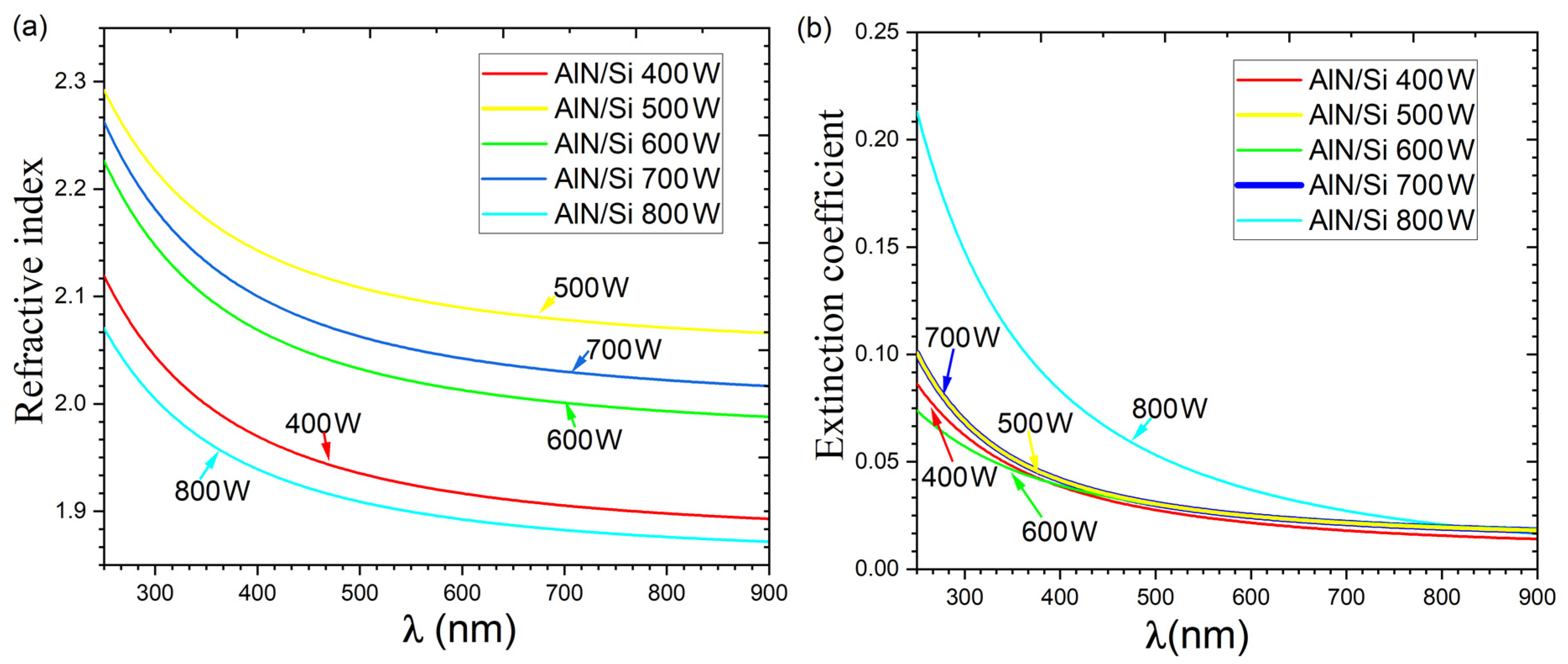
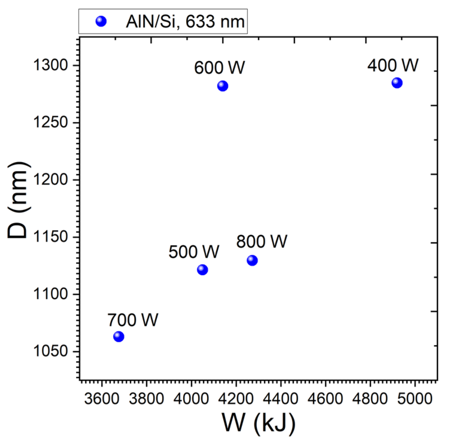
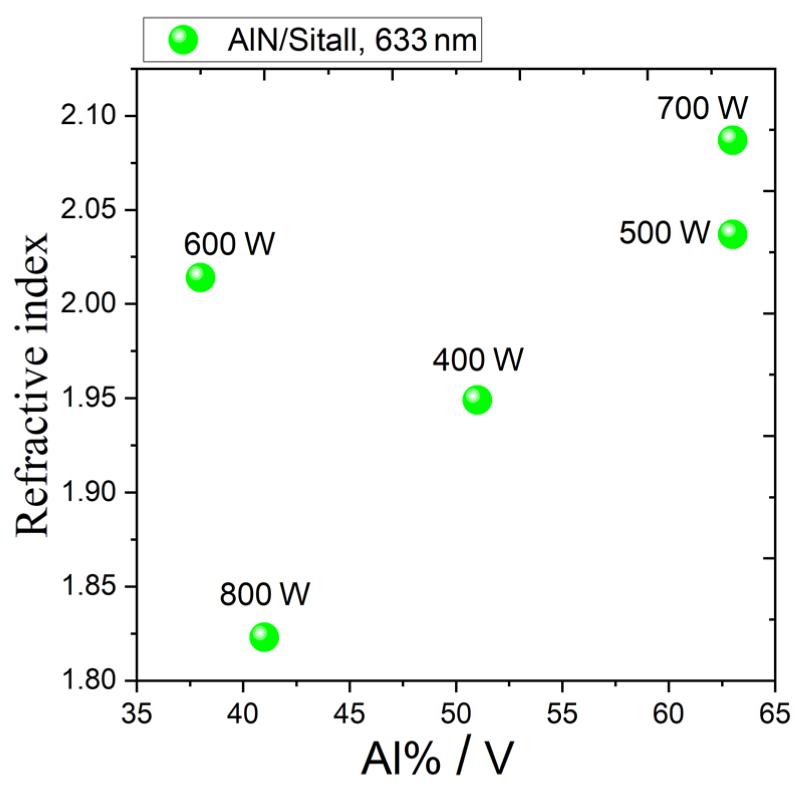
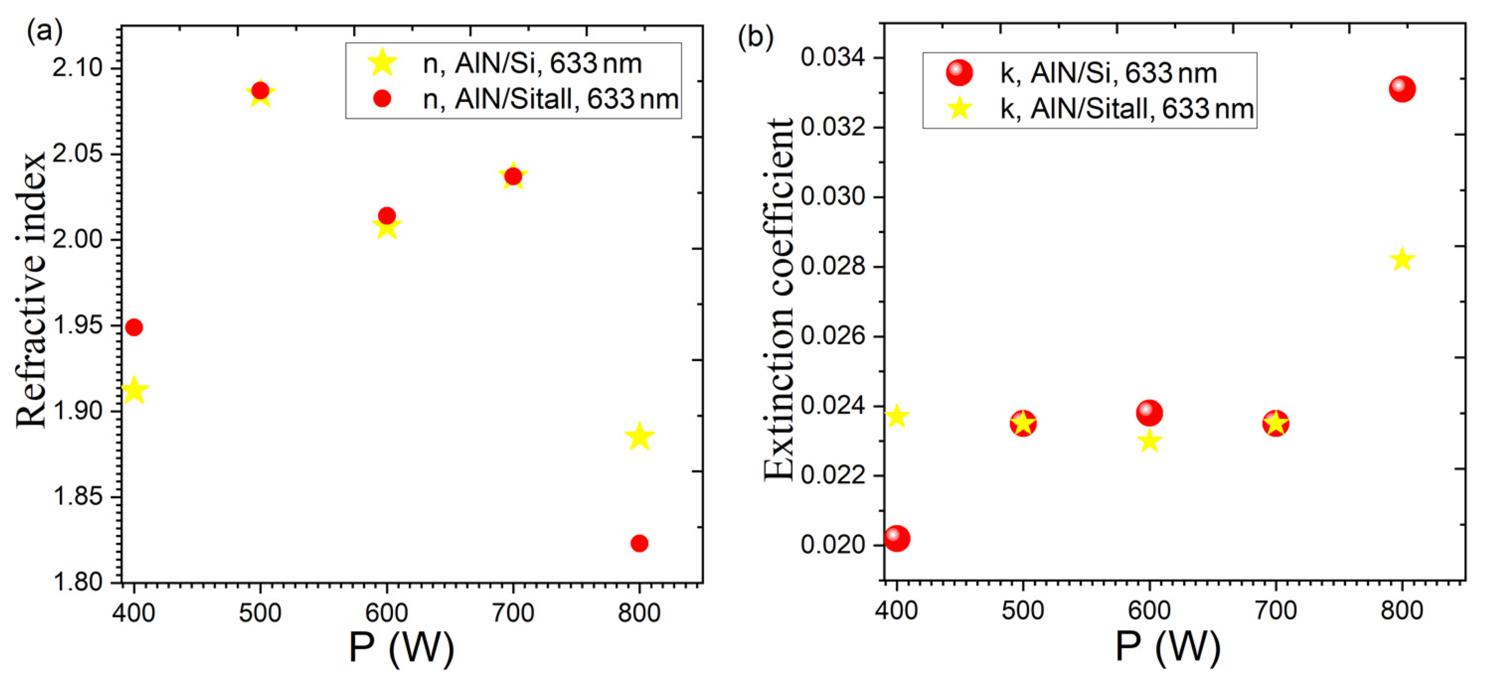
3.1. Ellipsometry Results

Figure 2 shows the dependences of the refractive index n and extinction coefficient k on the wavelength for various samples of thin films. It can be seen that in the case of the AlN film sample obtained at 800 W, the lowest refractive indices and the highest absorption coefficients were achieved. At the same time, for films obtained at magnetron power in the range 400–700 W, similar values of absorption coefficients are observed, and the refractive index n at the same wavelength does not depend linearly on the power of the magnetron. For the presented ellipsometry data, there is no clear correlation with GIXRD data (See Section 3.3). Thus, a film sample obtained at 400 W, according to the diffraction pattern (See Section 3.3), has the highest intensity of the 002 peaks, which, in theory, can be associated with the degree of orientation of the crystals in the film. However, the refractive index n here is closest to the sample deposited at 800 W, which is X-ray amorphous. Most likely, the samples of the studied series have different looseness and porosity, the values of which may not depend on the crystal structure of the objects under study. However, data on porosity and looseness are also important for evaluating material characteristics.
All reconstructed parameters for this series of samples are presented in Table 2. From the dispersion dependences of the refractive and absorption indices, the values at the wavelength of the He–Ne laser (633 nm) were taken.
A direct dependence of the AlN layer thickness on the magnitude of the magnetron operation work W (the product of the power and the operating duration) was observed (See Figure 3) for all samples, except for the sample grown at a magnetron power of 600 W. In this sample, a significantly higher thickness value is observed compared to the rest of the samples in the series. Assuming that the amount of material sputtered from the magnetron target is proportional to the operation of the magnetron, the same film thickness should be obtained with the same work. The thickness for this sample turned out to be higher than the expected one, which indicates its reduced physical density.
A direct dependence of the refractive index n on the quality of the Al–AlN interface is also observed (See Figure 4), except for the sample with a magnetron power of 600 W, which had the most developed Al relief.
It can be seen from Figure 5 that monotonic dependences of the refractive index and absorption on the power of the magnetron are not observed in the samples. We denote that the samples obtained at the highest and lowest magnetron power have low refractive indices n, which corresponds to the worst crystalline perfection and low physical density. Similar observations were made by other authors earlier in [43,44].

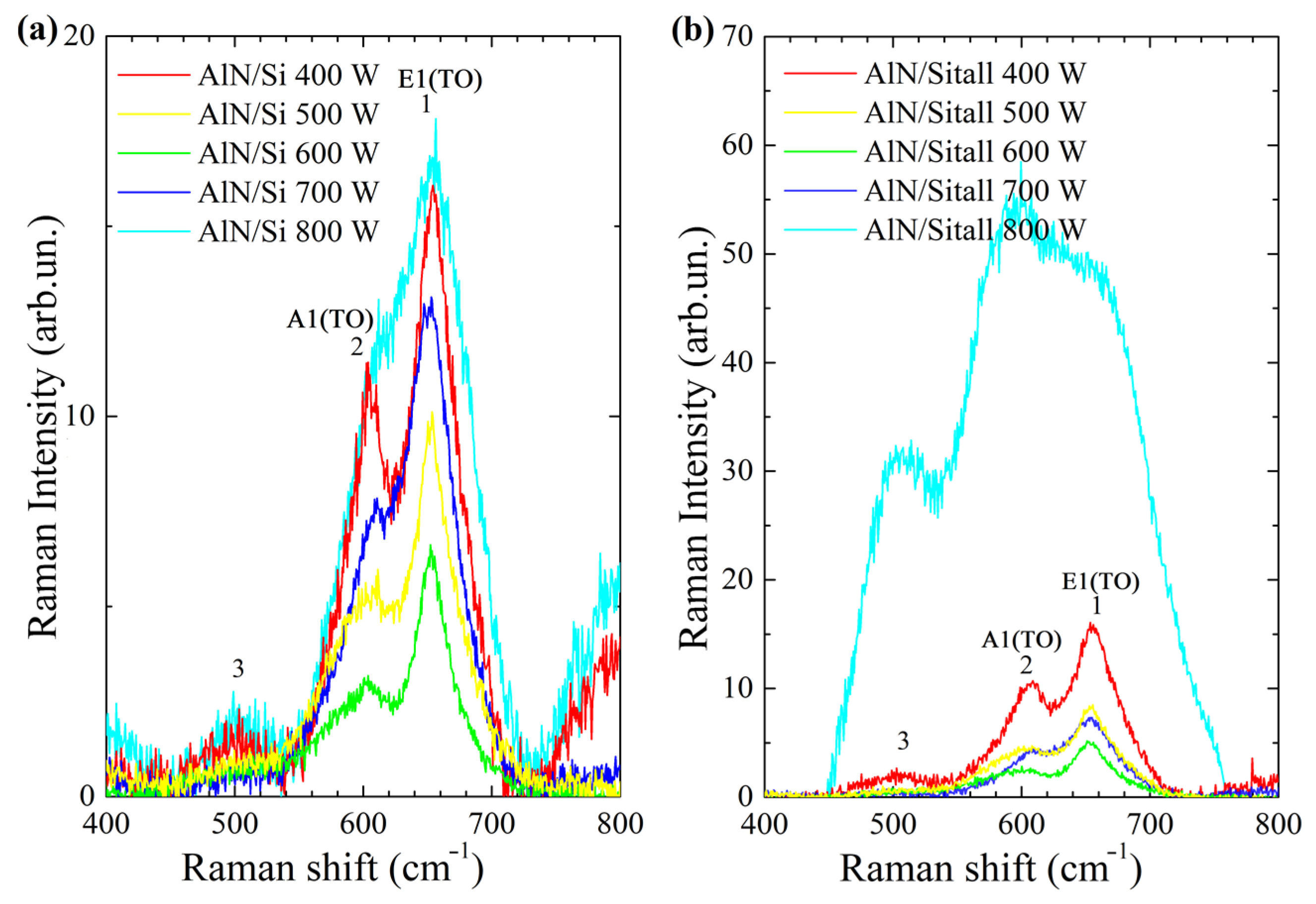
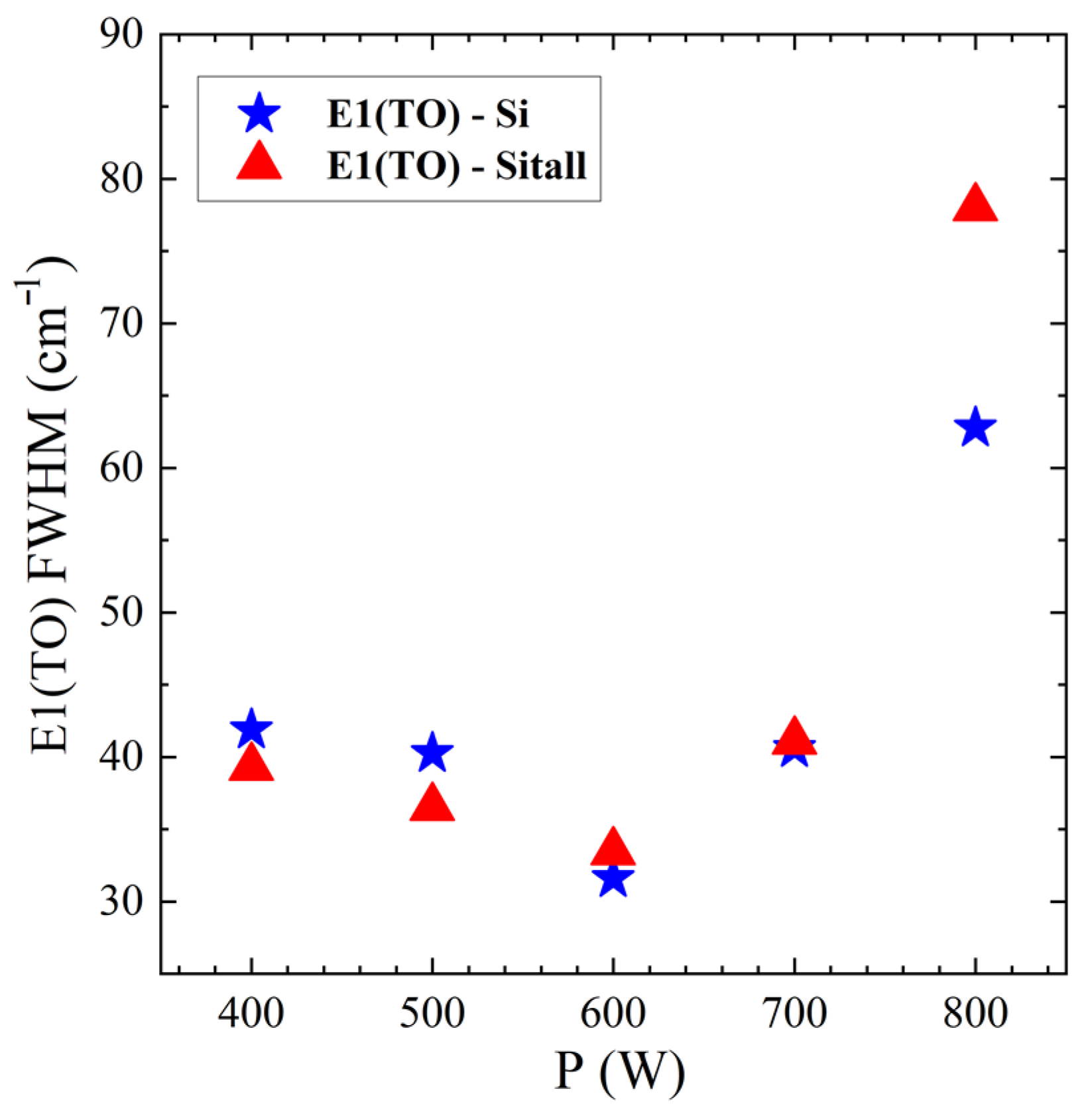
3.2. Raman Scattering Results

AlN crystals have a wurtzite-type structure and contain four atoms in a primitive cell; therefore, the phonon dispersion of AlN contains 12 modes, three of which are acoustic and nine optical, as mentioned above. The Raman method was used to study the most intense modes, A1(TO) and E1(TO), which have frequencies in the range of 600–650 cm−1 [45,46,47,48]. This method also makes it possible to characterize the crystal structure in AlN films (single–crystal, polycrystalline, or amorphous). For single–crystal AlN, peaks of vibration modes A1(TO), E2(TO), and E1(TO) are observed in the range of 600–650 cm−1, and in the case of nanocrystalline AlN, the last two peaks merge into one due to broadening [49]. According to the model presented in [49,50], the broadening of peaks can be related both to the size of crystallites and to the imperfection of the crystal structure (impurity atoms, inhomogeneous stresses, etc.). The more perfect the structure of crystallites, the smaller the width of the peaks from phonon modes, which are observed in the Raman method. Figure 6 shows the measured Raman spectra of all AlN samples grown on various substrates with varying magnetron power. It is seen that the observed peaks in the spectra are near (in position) to the peaks of vibrational modes A1(TO) and E1(TO) for AlN hexagonal symmetry and also have a strong broadening (40–50 cm−1), which allows us to state nanocrystallinity, or about the amorphous structure of the obtained films.
Table 3, as well as Figure 6, demonstrates the results of the analysis of the obtained peaks for the AlN–600 samples on two types of substrates: silicon and glass-ceramic (i.e., sitall). It can be seen from the presented data that the width of the peaks increases significantly (by a factor of 1.5–2) for samples grown at a magnetron discharge power of 800 W. This, together with GIXRD data, Raman confirms the amorphous nature of the obtained AlN layer. This trend is typical for films regardless of the type of initial substrate since the AlN layer is initially deposited onto the Al layer.
Figure 7 shows the dependences of the widths of the Raman peak of the E1(TO) mode on the magnetron power at which AlN films were deposited for two series of samples. For AlN film samples deposited at 600 W, the peak width is the smallest of the entire series for both. However, according to the obtained GIXRD data, the samples have the smallest coherent scattering region (CSR) sizes. It should be noted that the half-width of the peaks, even for these samples, is much larger than the half-width for single crystals [49] and is comparable with other samples of the series [50]. This may indicate that the phonon coherence length is smaller than the CSR calculated from the GIXRD data. In general, according to the Raman analysis, it can be suggested that with an increase in the power of the magnetron discharge to 800 W, a sharp deterioration in the crystallinity of the AlN layer occurs.

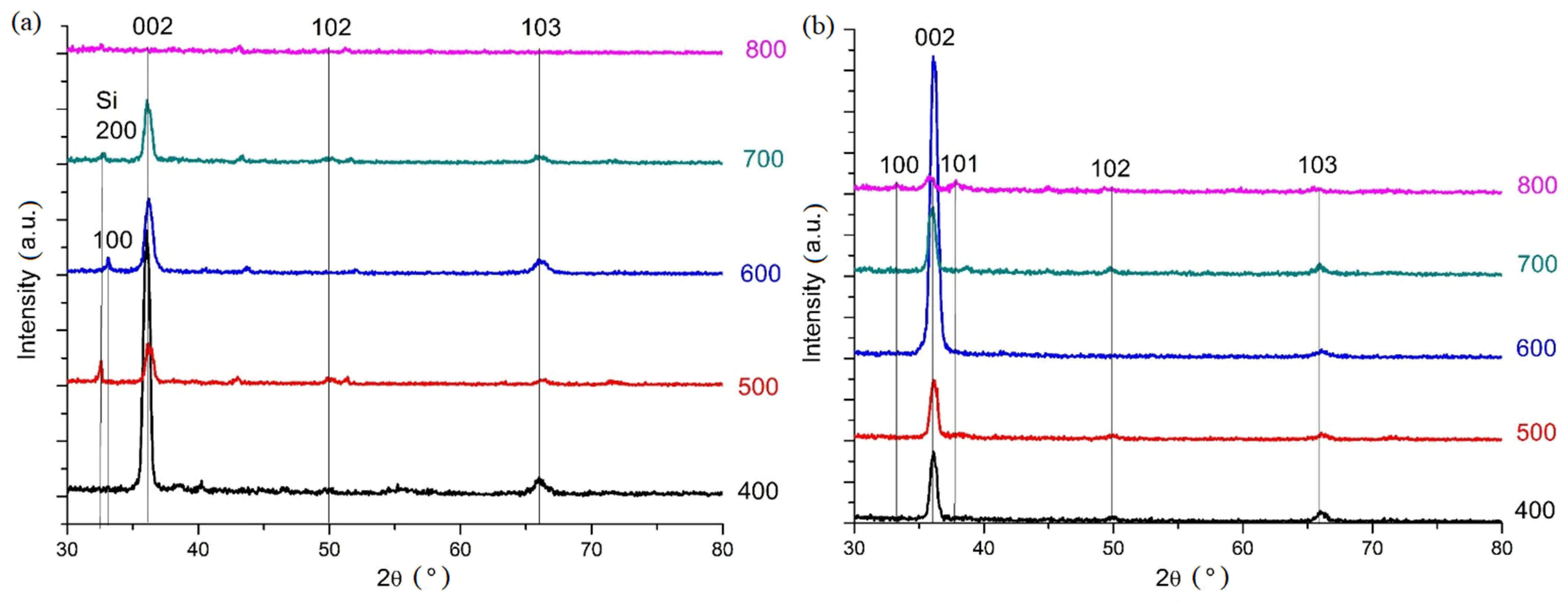
3.3. Grazing Incidence X-ray Diffraction Results
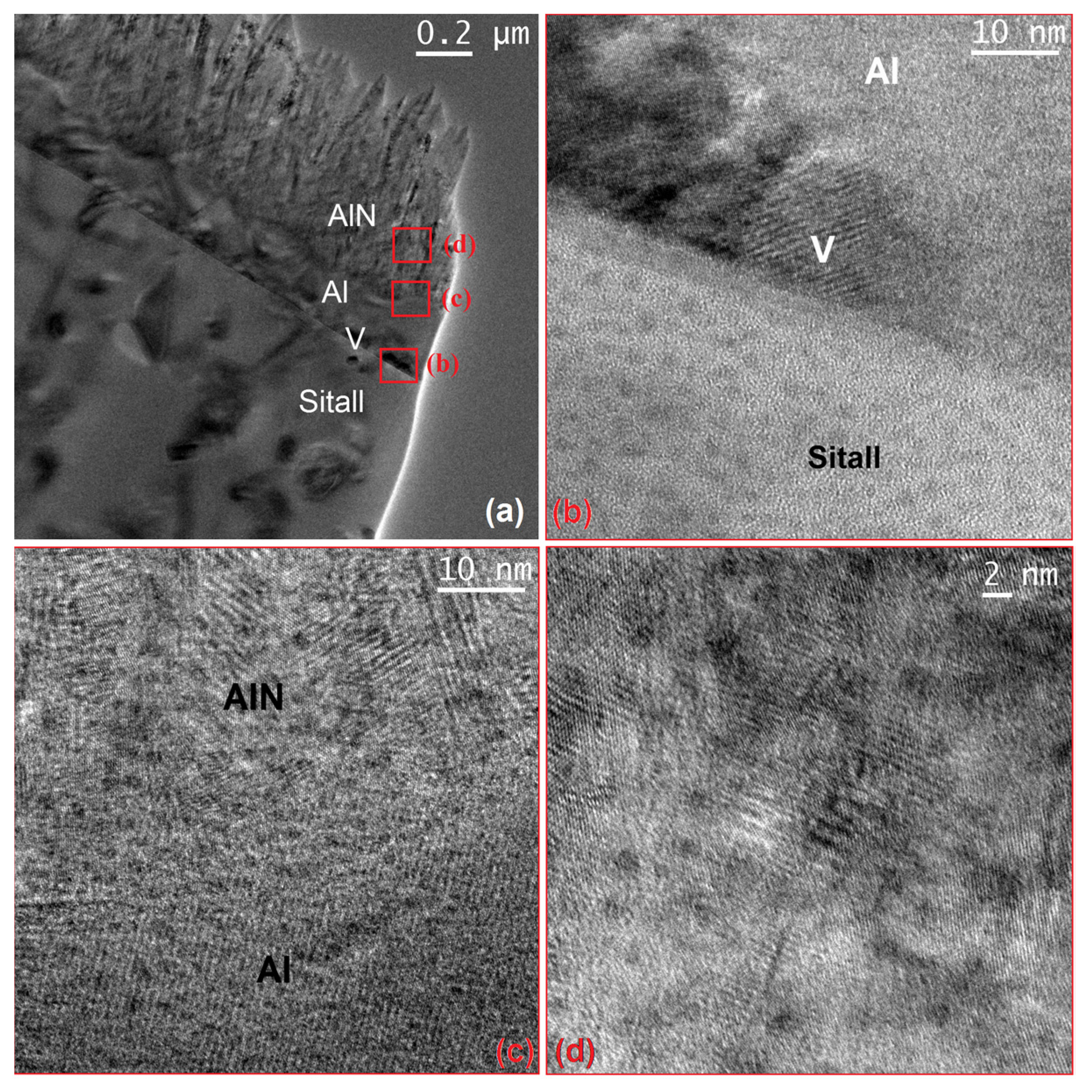
X-ray diffraction patterns of the studied AlN–Al–V films are presented in Figure 8, where a layer of aluminum nitride was deposited at different powers of the magnetron discharge on different substrates. During the analysis of diffraction patterns, it was revealed that for samples grown at a magnetron discharge power of 400–700 W, a hexagonal wurtzite-type AlN phase was obtained (PDF No. 25–1133). No other phases were observed except for low-intensity reflections from the silicon substrate. Their observation in the Grazing Incidence X-ray Diffraction (GIXRD) geometry is explained by the fact that the formed film did not completely cover the substrate, and therefore, part of the silicon was irradiated by the beam during the shooting. In the case of the sample obtained at a power of 800 W, the diffraction pattern also shows reflections that can be attributed to AlN, but their intensity decreases significantly up to complete extinction.
It should be noted that AlN in the obtained films has the required c–axis texture, in which the crystallites are predominantly oriented with the (002) planes towards the surface. This is evidenced by an increase in the intensity of the 002 peaks with partial or complete extinction of the remaining peaks. However, the crystal texture of the AlN layer is not ideal. The presence of reflections 102 and 103 is also noticeable in the diffraction pattern, which may indicate a deviation of some of the crystallites from the texturing axis associated with the competitive growth of crystallites in other directions [39]. At the same time, in the case of a sample grown at 800 W on a sitall substrate, it is seen that the diffraction pattern shows a set of reflections for misoriented AlN (100, 002, 101, 102, and 103), while their low intensity and large width indicate a transition to a nanocrystalline state with small particle size. In the case of a silicon substrate, peaks are not observed due to their extinction. However, it can be assumed that the film is in a phase state close to that of the film sample on sitall. Interestingly, the highest intensity of the 002 peaks in the case of samples on silicon is observed for the sample obtained at 400 W, while on sitall, the intensity is maximum for the sample obtained at 600 W. This, in particular, can be associated with the degree of orientation of the film crystallites [51].
For the obtained estimated values of the average crystallite size (See Table 4), it can be noted that the CSR sizes mainly vary in the range of 60–150 nm. The smallest crystallite sizes are observed for the sitall-based AlN film fabricated at 800 W, as well as for the samples obtained at 600 W. At the same time, for these samples, the parameters and volume of the unit cell are increased compared to the standard ones (a = 3.1114 Å, c = 4.9792 Å, V = 41.75 Å3). In general, it is noticeable that the cell volume increases with increasing magnetron power for a film on a silicon substrate and depends nonlinearly in the case of films on sitall. Taken together, this allows us to make a conclusion about the accumulation of a significant number of defects in the crystal structure and the deterioration of the quality of the crystal structure with an increase in the power of the magnetron discharge.

3.4. TEM Results

A thin transverse section (lamella) of an AlN–600 sample was prepared for visualization by TEM (Figure 9a). This sample, given the features that were observed during its study by other methods, was expected to possess a peculiar microstructure that, apparently, required additional attention. The sample surface was severely damaged, as the sample surface was etched at 200 nm to obtain the desired lamella thickness due to the specifics of the FIB-SEM sample preparation procedure.
The images were taken in several areas of the sample by HR-TEM: Sitall–V–Al boundaries (Figure 9b), AlN–Al boundary (Figure 9c), and AlN volume (Figure 9d). The regions are marked on the micrograph of the entire film in Figure 9a in red. For Al and V layers in high resolution, a high roughness of the interface with neighboring layers is noticeable. A large number of defects (nanopores) are observed in the AlN layer, the sizes of which vary from 2 to 3 nm.

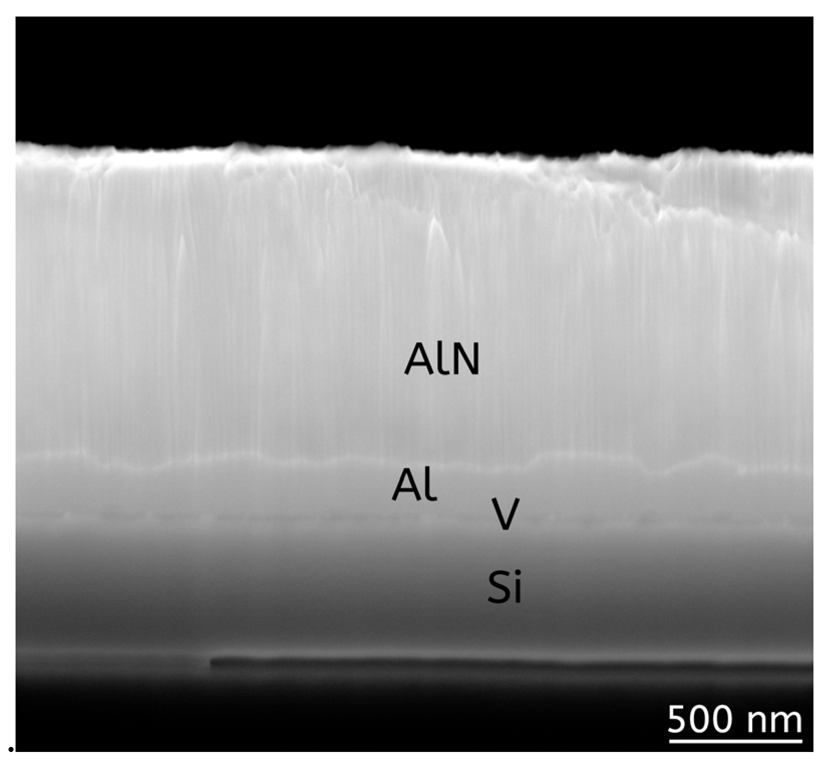
3.5. SEM Cross-Section Results

SEM image of a cross-section of an AlN–600 sample is shown in Figure 10. Images of the rest of the samples from the series are presented in Figure S1 in Supplementary Materials.
An analysis of the obtained images showed that the Al layer has an uneven and “bumpy” surface, which, in turn, may indicate the absence of directionality in the growth of Al crystallites during their deposition. As a result, the AlN layer becomes misoriented and rough, which could affect the piezoelectric properties of the AlN film, as well as the velocity of acoustic waves in the volume and on the surface. As in the TEM images, Figure 10 shows the heterogeneity (porosity) of the vanadium layer. The thicknesses of the layers were also estimated, which turned out to be somewhat different from the assessment of the technologists based on monitoring by a quartz resonator (Table 5).
The thicknesses of the film layers vary depending on their power and deposition duration. The AlN–400 sample is closest to the declared thickness values since the sample was deposited longer than the others, and, as a result, the crystallites in it appear to be less defective.

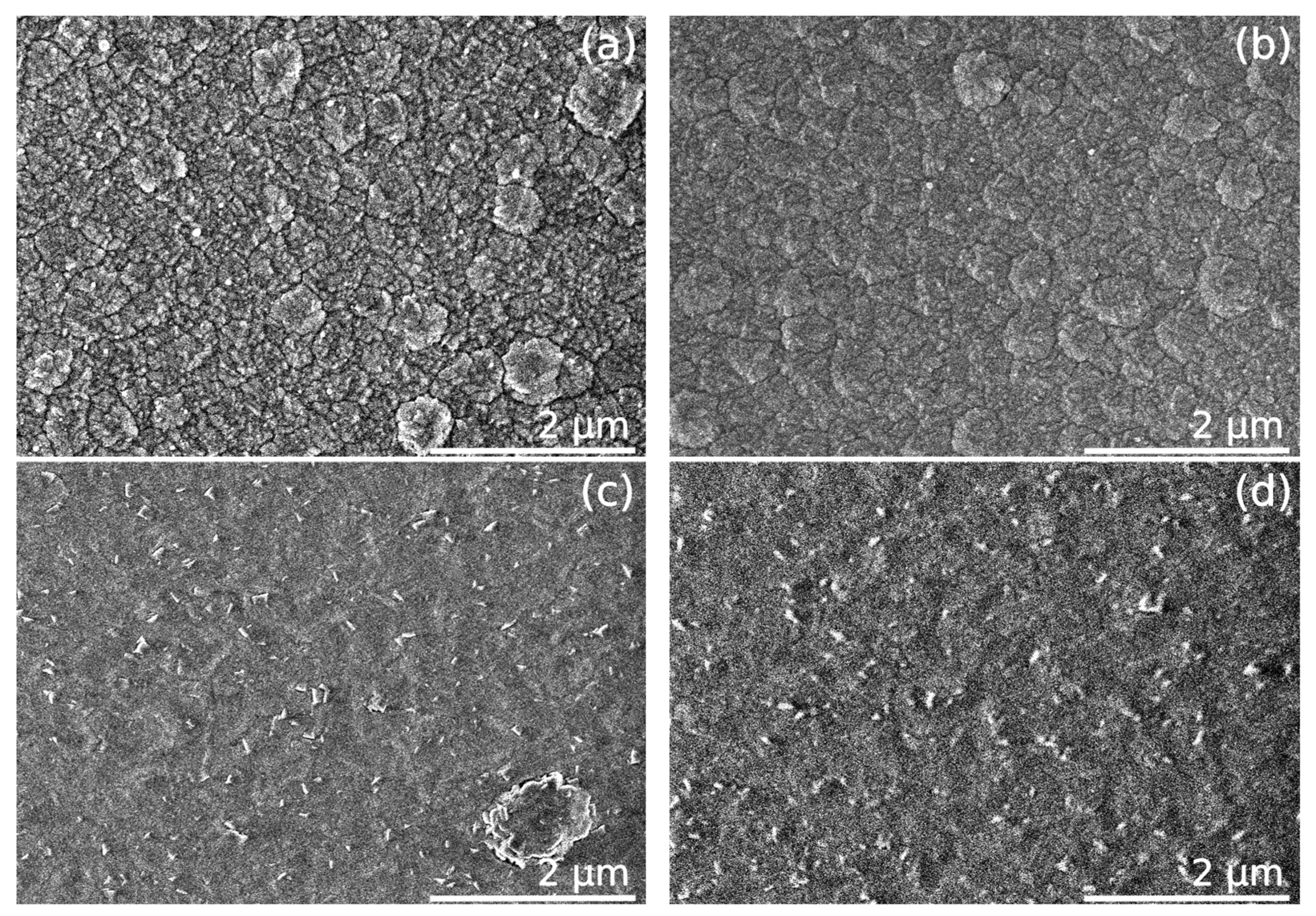
3.6. SEM and SEM-EDS Results in Top View Study
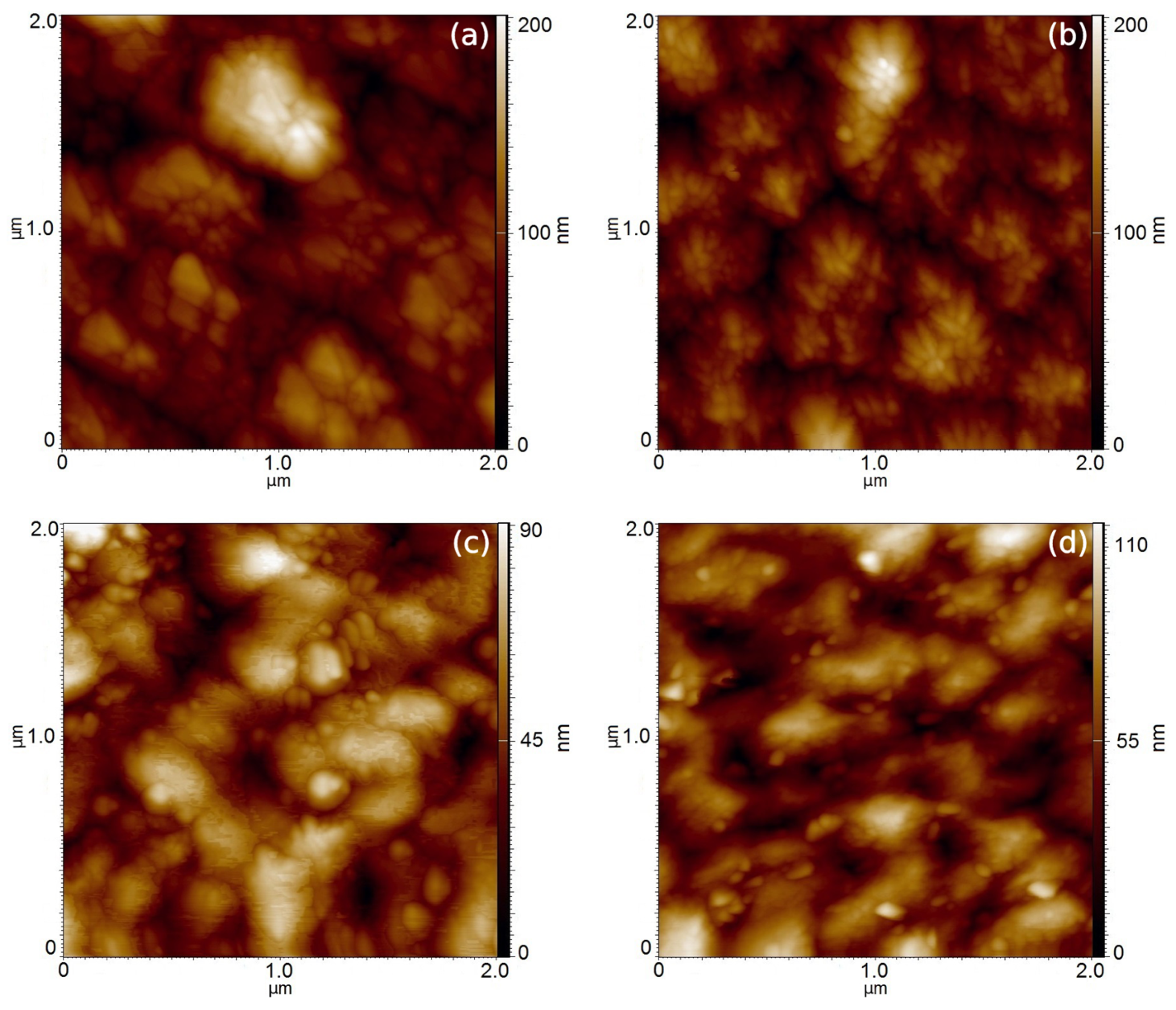
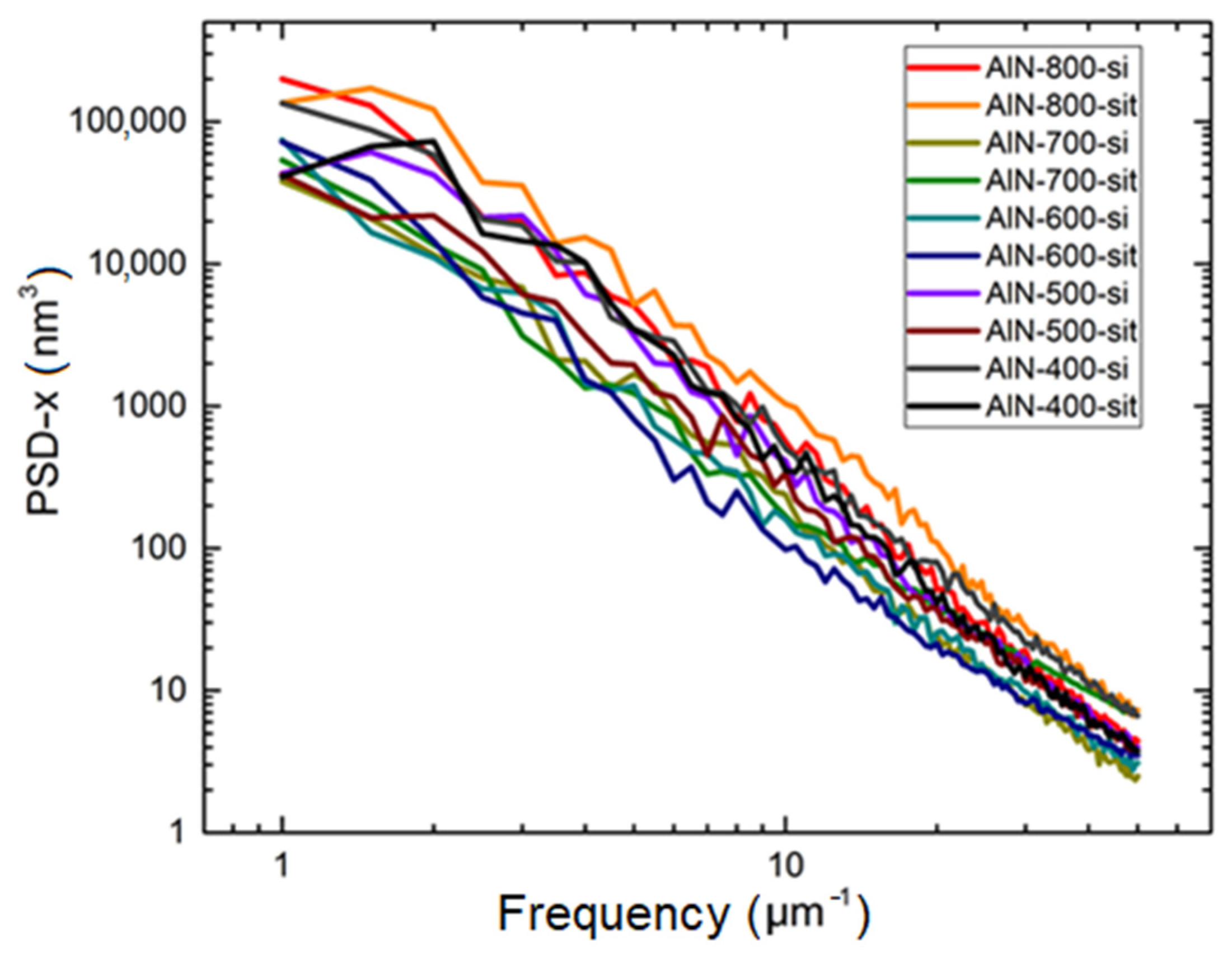
SEM images of the surface of thin films on the example of AlN–800 and AlN–600 samples (on both substrates) are shown in Figure 11. More details about all images can be found in Figure S2 in Supplementary Materials.
The obtained data on the surface visualization by the SEM method correlates with the AFM data. Samples of thin films grow in the form of close-packed vertically oriented hexagons and emerge on the surface in the form of dendritic structures, and their form does not depend on the substrate material. However, it was noticed that the appearance of the structures on the surface of the AlN–600 sample has slight visual differences. Elemental analysis of the EDS of the surface layers of all AlN film samples was also performed. The obtained values of the concentration of the content of elements in the composition of the samples are presented in Table 6.
From the analysis of Table 6, it can be concluded that in all the studied samples, there is an excess of Al, while the stoichiometric ratio of elements in AlN is rather far from the ideal ratio of 1 to 1. The AlN–800 film grown at the maximum power of the magnetron discharge in the composition has the highest content of oxygen and carbon impurities, as well as the lowest content of nitrogen. The closest to the optimum are the AlN–600 and AlN–700 films since they contain the lowest amount of impurity oxygen and carbon, as well as the highest content of nitrogen. This is precisely why the surface morphology of AlN–600 film has visual differences from the surfaces of other AlN film samples. It should also be noted that with a decrease in the power of the magnetron discharge, the oxygen content in the films decreases. The presence of 1–2% copper in the films is observed as copper is present in the composition of the aluminum target, which, during the deposition of films, is deposited in small amounts on the sample. This may also be the result of insufficient cleaning of the target before sputtering. The clarity and contrast of SEM images correlate with the proportion of aluminum in the sample. The greater the concentration of Al (conductive material), the more contrasted image is visualized since the conductive material allows the accumulated electric charge from the SEM beam to be removed from the dielectric bulk.

3.7. AFM Results

Scanning probe microscopy results for the films are demonstrated in Figure 12 and Figure S3 in Supplementary Materials as images representing the developed relief.
Based on the visual analysis of the obtained images, it was concluded that the type of structures on the surface of thin films does not depend on the substrate material. In addition to standard 2D images, numerical values of the roughness parameters of AlN film samples were also obtained by AFM (Table 7).
Regarding the roughness analysis, in the case of mathematically flat films, the film roughness parameters should tend to be zero. Although in order to perform the real technological procedures (e.g., deposition of electrodes on the film surface), the optimal roughness values typically are in the range from 5 to 7 nm. The AlN–700 sample on silicon is closest to the satisfactory roughness values, i.e., its roughness is 10 nm. The AFM method also allowed calculating the advanced numerical values of power spectral density (PSD) of the surface roughness of the samples by fast axis (x) of AFM scanning (See Figure 13).
The amount of large-scale inaccuracies (upper left part of Figure 13) is small, while most of the roughness is based on small-volume features (See the enlarged value of small-volume features of AFM morphology in the down-right part of Figure 13). During the analysis of the curves in Figure 13 and Table 7, it was found that the highest difference in surface roughness is observed in samples AlN–800 (roughest) and AlN–700 (least rough), the smoothest sample in the frequency range 4–13 μm−1, which corresponds to irregularities with characteristic sizes of 77–150 nm is the AlN–600–sit sample. The surfaces of the AlN–800 samples are the roughest since their curves are clearly higher than those of other samples. As can be seen from the presented roughness spectra, there is no unambiguous dependence of the AlN surface roughness from the substrate material, i.e., from Si or sitall.

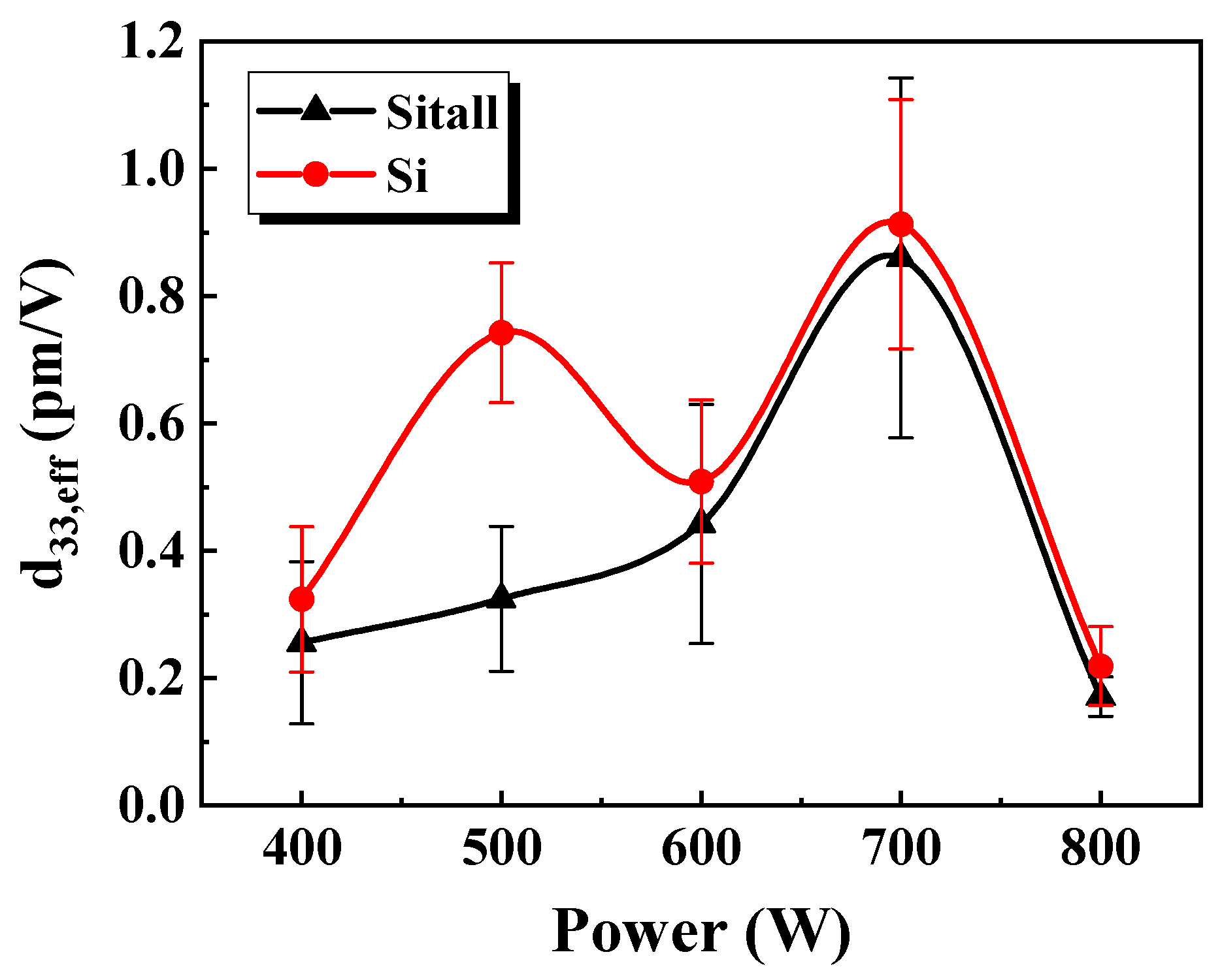
3.8. SSMP Piezoresponse Results

Figure 14 presents the results of determining the effective piezoelectric coefficient in the studied AlN films. It is visible that the d33,eff values of the films differ little for the two types of substrates within the range of values, except for the d33,eff value for the AlN–500 film on the sitall substrate.
The reduced value of d33,eff for this film is probably due to poor electrical contact between the electrode of the sample holder and the Al layer, which could lead to a lower amplitude of the alternating voltage between the probe and the Al layer and, accordingly, a lower piezoresponse. For the silicon substrate, higher average values of d33,eff, are systematically observed, which may be due to its conductivity, which contributes to a more uniform distribution of the electric potential over the Al layer. This is also evidenced by the smaller spread of d33,eff values for AlN films on silicon substrates. It can be seen from Figure 14 that with an increase in the power of the magnetron discharge from 400 to 700 W, the effective piezoelectric coefficient of the films increases and reaches its maximum value at 700 W. At a discharge power of 800 W, the piezoelectric properties of the films noticeably degrade, which correlates with the deterioration of AlN crystallinity and stoichiometry. A violation of the described trend is a decrease in the average value of d33,eff, at a discharge power of 600 W, which may be due to structural features of AlN–600 films, namely, reduced crystallite size and an increased unit cell volume (GIXRD data), as well as increased porosity (ellipsometry data and TEM). The effective piezoelectric coefficient reaches the highest values at a magnetron discharge power of 700 W, which may be due to the relatively high structural perfection of the AlN film within this series, as evidenced by the combination of the following characteristics: low surface roughness (AFM data), high structural density, and low porosity (ellipsometry data), high degree of stoichiometry (SEM-EDS data), increased crystallite size (GIXRD data), and relatively high resistivity (electrophysical measurements data).

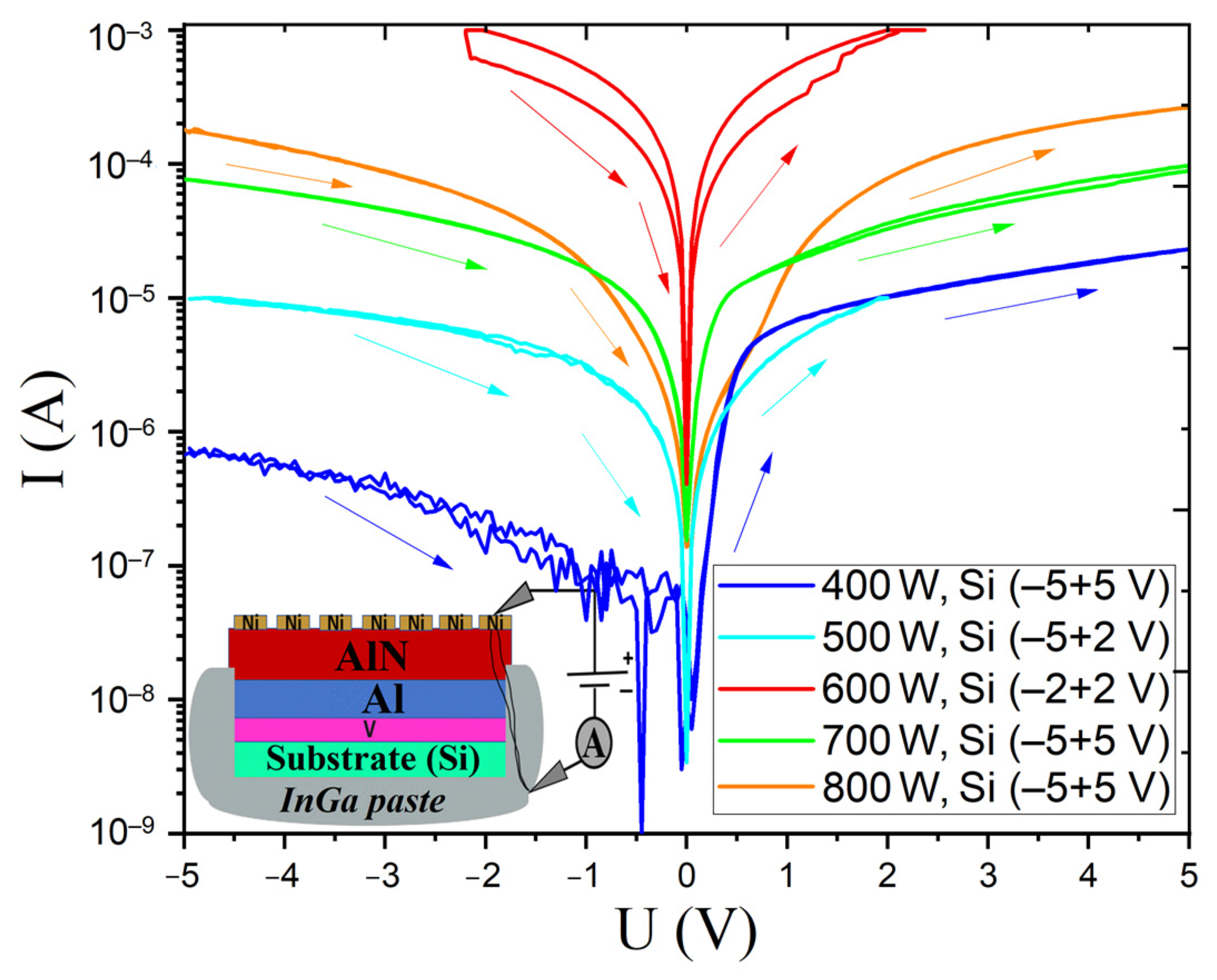
3.9. I–V Curve Analysis

Figure 15 shows the current-voltage characteristics of AlN layers in thin AlN–Al–V composite films on a silicon substrate obtained at different magnetron discharge powers. The measurement scheme is shown in the inset (See the left-down corner in Figure 15).
Since the flowing currents are high, we did not create special guard rings surrounding the measuring electrode (such rings are usually established when measuring the volume resistance of dielectrics to equalize the potential of the measuring electrode so as not to take into account the surface current). Further, we assume that the lower electrode forms an ohmic contact with the AlN film due to the transition layer between the Al and AlN films, which creates conductive shunts. A comparison of the curves shows that there is no direct relationship between the resistance and the conditions for obtaining films (the power of the magnetron discharge). The highest currents are observed in the AlN–600–si sample, reaching a value of 10−3 A already at ±2 V (the meter switches to the current mode due to the set current limit of 10−3 A). According to GIXRD data, this sample has the smallest crystallite sizes and an increased unit cell volume, indicating the presence of a significant number of defects in the crystal structure. High currents are also observed in the AlN–800–si sample, which is also strongly defective up to amorphization and has a significant excess of the Al content. For samples obtained at powers of 700, 500, and 400 W, the curves exhibit asymmetry depending on the polarity of the voltage applied to the upper electrode. It is known that the direct deposition of metal films on the AlN surface creates a Schottky barrier with high resistance [52]. This effect manifests itself in the I–V curve. The asymmetry is most pronounced for the AlN–400–si sample, which has the lowest currents. Structural studies have shown that this film is maximally textured in the 002 direction. The resistivities calculated from the I–V curve (for U = +2 V) of the studied AlN films are given in Table 8.
Electrophysical studies of the AlN films grown on silicon substrates revealed that the resistance was highest in AlN layers fabricated at the lower power of the magnetron discharge. The highest resistance, being the anticipated characteristic of a dielectric structure, directly correlates with the structural perfection of the layer material.

4. Conclusions

The samples were grown in the magnetron power range of 400–700 W and presented rather similar crystal structure and texture. However, they do not demonstrate the ideal c–axis structure of AlN thin films from the literature. An AlN film sample grown at a magnetron power of 800 W showed the worst quality of the crystal structure according to GIXRD and Raman data, as well as significant absorption in the optical range and the highest surface roughness in the studied series. The reason for such observation is the misalignment of the AlN–Al layer interface. A good correlation is observed between the thickness of the AlN films and the total energy expended by the magnetron for sputtering the target, except for the AlN sample grown at a power of 600 W. This sample, presumably, had a lower mass density. The same conclusion is confirmed visually by the TEM results in the form of repeated microstructure defects.
Nevertheless, the refractive index of this sample is quite high, and the phonon scattering peak in Raman has the narrowest contour, which confirms the high quality of the crystal structure at the nanoscale. Therefore, we highlight the methodological value of the present work for other authors who investigate similar films and observe similar results, which indeed do not present disagreements. There is a correlation between the refractive index and the quality of the Al–AlN interface, which is characterized by the volume filling factor νAl. The AlN film fabricated at 600 W also appears to be of high interest because it shows an anomalously high value of the refractive index and the most developed aluminum surface in the interface layer. Specific results of the AlN film grown under the 600 W power present various interesting features, so the balance between nanoscale structural details and macroscale properties should be considered systematically.

Supplementary Materials

The following supporting information can be downloaded at https://www.mdpi.com/article/10.3390/coatings13020223/s1; Figure S1: SEM cross-section images of AlN thin films on a silicon substrate; Figure S2: SEM images of AlN thin films on silicon and sitall substrates; Figure S3: AFM images of AlN thin films on silicon and sitall substrates.

Author Contributions

Conceptualization, L.V.B., V.I.S. and P.V.G.; Data curation, V.S.K. and L.V.B.; Formal analysis, A.V.K., I.A.A., G.N.K., N.A.C., N.A.D. and V.S.K.; Funding acquisition, V.I.S. and P.V.G.; Investigation, M.I.M., A.V.K., G.A.H., V.A.V., I.A.A., I.D.Y., G.N.K., E.A.S., N.A.C., N.A.D., A.N.B. and V.S.K.; Methodology, A.V.K.; Project administration, P.V.G.; Resources, N.A.C. and V.I.S.; Supervision, V.I.S.; Validation, G.N.K., V.I.S. and P.V.G.; Writing—original draft, M.I.M., A.V.K., N.A.C., N.A.D., V.S.K. and P.V.G.; Writing—review & editing, M.I.M., N.A.D., V.I.S. and P.V.G. All authors have read and agreed to the published version of the manuscript.

Funding

This research was funded by the Ministry of Science and Higher Education of the Russian Federation, grant No. FSUS-2020-0029, in terms of sample analysis and method development (M.I.M., A.V.K., V.A.V., I.A.A., I.D.Y., P.V.G.). The sample fabrication and partial sample experimental examination (N.A.C., N.A.D., A.N.B., V.S.K., L.V.B., V.I.S.) was carried out within the framework of the State assignment for scientific research to the Omsk Scientific Center RAS from the Ministry of Science and Higher Education of the Russian Federation, grant No. FWEE-2021-0005.

Institutional Review Board Statement

Not applicable.

Informed Consent Statement

Not applicable.

Data Availability Statement

The data presented in this study are available on request from the corresponding authors.

Acknowledgments

The authors acknowledge the Shared Research Center “VTAN” of the Novosibirsk State University supported by Minobrnauki of Russia by agreement #075-12-2021-697. The authors acknowledge the Shared Equipment Center “National Center for the Study of Catalysts” at the Boreskov Institute of Catalysis for the provision of TEM preparation and analysis. The authors acknowledge A. O. Geydt and V. O. Isaev for their help with translation and editing and A. L. Aseev for valuable discussions.

Conflicts of Interest

The authors declare no conflict of interest.

References

  1. Iqbal, A.; Mohd–Yasin, F. Reactive sputtering of aluminum nitride (002) thin films for piezoelectric applications: A review. Sensors 2018, 18, 1797. [Google Scholar] [CrossRef] [PubMed] [Green Version]
  2. Beshkova, M.; Yakimova, R. Properties and potential applications of two–dimensional AlN. Vacuum 2020, 176, 109231. [Google Scholar] [CrossRef]
  3. Cimalla, V.; Pezoldt, J.; Ambacher, O. Group III nitride and SiC based MEMS and NEMS: Materials properties, technology and applications. J. Phys. D Appl. Phys. 2007, 40, 6386. [Google Scholar] [CrossRef]
  4. Fei, C.; Liu, X.; Zhu, B.; Li, D.; Yang, X.; Yang, Y.; Zhou, Q. AlN piezoelectric thin films for energy harvesting and acoustic devices. Nano Energy 2018, 51, 146–161. [Google Scholar] [CrossRef]
  5. Elfrink, R.; Kamel, T.M.; Goedbloed, M.; Matova, S.; Hohlfeld, D.; van Andel, Y.; van Schaijk, R. Vibration energy harvesting with aluminum nitride–based piezoelectric devices. J. Micromech. Microeng. 2009, 19, 094005. [Google Scholar] [CrossRef] [Green Version]
  6. Yen, T.T.; Hirasawa, T.; Wright, P.K.; Pisano, A.P.; Lin, L. Corrugated aluminum nitride energy harvesters for high energy conversion effectiveness. J. Micromech. Microeng. 2011, 21, 085037. [Google Scholar] [CrossRef]
  7. Suter, J.J.; Bryden, W.A.; Kistenmacher, T.J.; Porga, R.D. Aluminium Nitride on Sapphire Films for Surface Acoustic Wave Chemical Sensors. Johns Hopkins APL Tech. Dig. 1995, 16, 288–295. [Google Scholar]
  8. Piazza, G.; Felmetsger, V.; Muralt, P.; Olsson, R.H., III; Ruby, R. Piezoelectric aluminum nitride thin films for microelectromechanical systems. MRS Bull. 2012, 37, 1051–1061. [Google Scholar] [CrossRef] [Green Version]
  9. Omori, T.; Kobayashi, A.; Takagi, Y.; Hashimoto, K.Y.; Yamaguchi, M. Fabrication of SHF range SAW devices on AlN/Diamond–substrate. In 2008 IEEE Ultrasonics Symposium; IEEE: Piscataway, NJ, USA, 2008; pp. 196–200. [Google Scholar] [CrossRef]
  10. Shelton, S.; Guedes, A.; Przybyla, R.; Krigel, R.; Boser, B.; Horsley, D.A. Aluminium Nitride Piezoelectric Micromachined Ultrasound Transducer Arrays; Solid–State Sensors, Actuators, and Microsystems Workshop: Hilton Head Island, SC, USA, 2012; pp. 291–294. [Google Scholar] [CrossRef]
  11. Rinaldi, M.; Zuniga, C.; Zuo, C.; Piazza, G. Super–high–frequency two–port AlN contour–mode resonators for RF applications. IEEE Trans. Ultrason. Ferroelectr. Freq. Control. 2010, 57, 38–45. [Google Scholar] [CrossRef]
  12. Ruby, R.; Bradley, P.; Larson, J., III; Oshmyansky, Y.; Figueredo, D. Ultra–miniature High–Q filters and duplexers using FBAR technology. In Proceedings of the 2001 IEEE International Solid-State Circuits Conference, Digest of Technical Papers. San Francisco, CA, USA, 7 February 2001; pp. 120–121. [Google Scholar] [CrossRef]
  13. Lee, R.R. Development of high thermal conductivity aluminum nitride ceramic. J. Am. Ceram. Soc. 1991, 74, 2242–2249. [Google Scholar] [CrossRef]
  14. Duquenne, C.; Besland, M.P.; Tessier, P.Y.; Gautron, E.; Scudeller, Y.; Averty, D. Thermal conductivity of aluminium nitride thin films prepared by reactive magnetron sputtering. J. Phys. D Appl. Phys. 2011, 45, 015301. [Google Scholar] [CrossRef]
  15. Guy, I.L.; Muensit, S.; Goldys, E.M. Extensional piezoelectric coefficients of gallium nitride and aluminum nitride. Appl. Phys. Lett. 1999, 75, 4133–4135. [Google Scholar] [CrossRef]
  16. Martin, F.; Muralt, P.; Dubois, M.A.; Pezous, A. Thickness dependence of the properties of highly c–axis textured AlN thin films. J. Vac. Sci. Technol. 2004, 22, 361–365. [Google Scholar] [CrossRef]
  17. Karabalin, R.B.; Matheny, M.H.; Feng, X.L.; Defaÿ, E.; Le Rhun, G.; Marcoux, C.; Hentz, S.; Andreucci, P.; Roukes, M.L. Piezoelectric nanoelectromechanical resonators based on aluminum nitride thin films. Appl. Phys. Lett. 2009, 95, 103111. [Google Scholar] [CrossRef] [Green Version]
  18. Ruby, R.C.; Bradley, P.; Oshmyansky, Y.; Chien, A. Thin film bulk wave acoustic resonators (FBAR) for wireless applications. IEEE Int. Ultrason. Symp. 2001, 1, 813–821. [Google Scholar] [CrossRef]
  19. Artieda, A.; Muralt, P. Fabrication and properties of High–Q AlN/SiO2 composite TFBAR’s for above IC oscillators. In 2007 IEEE Ultrasonics Symposium; IEEE: Piscataway, NJ, USA, 2007; pp. 1164–1167. [Google Scholar] [CrossRef]
  20. Artieda, A.; Barbieri, M.; Sandu, C.S.; Muralt, P. Effect of substrate roughness on c–oriented AlN thin films. J. Appl. Phys. 2009, 105, 024504. [Google Scholar] [CrossRef]
  21. Iriarte, G.; Rodríguez, J.G.; Calle, F. Synthesis of c–axis oriented AlN thin films on different substrates: A review. Mater. Res. Bull. 2010, 45, 1039–1045. [Google Scholar] [CrossRef]
  22. Riah, B.; Camus, J.; Ayad, A.; Rammal, M.; Zernadji, R.; Rouag, N.; Djouadi, M.A. Hetero–Epitaxial Growth of AlN Deposited by DC Magnetron Sputtering on Si (111) Using a AlN Buffer Layer. Coatings 2021, 11, 1063. [Google Scholar] [CrossRef]
  23. Chung, C.J.; Chen, Y.C.; Cheng, C.C.; Wei, C.L.; Kao, K.S. Influence of Surface Roughness of Bragg Reflectors on Resonance Characteristics of Solidly–Mounted Resonators. IEEE Trans. Ultrason. Ferroelect. Freq. Contr. 2007, 54, 802–808. [Google Scholar] [CrossRef]
  24. Sanz–Hervas, A.; Vergara, L.; Olivares, J.; Iborra, E.; Morilla, Y.; Garcia–Lopez, J.; Clement, M.; Sangrador, J.; Respaldiza, M.A. Comparative study of c–axis AlN films sputtered on metallic surfaces. Diam. Relat. Mater. 2005, 14, 1198–1202. [Google Scholar] [CrossRef]
  25. Chen, Q.; Lifen, Q.; Qing–Ming, W. Property characterization of AlN thin films in composite resonator structure. J. Appl. Phys. 2007, 101, 084103. [Google Scholar] [CrossRef]
  26. Iriarte, G.F.; Bjurstrom, J.; Westlinder, J.; Engelmark, F.; Katardjiev, I.V. Synthesis of c–axis–oriented AlN thin films on high–conducting layers: Al, Mo, Ti, TiN, and Ni. IEEE Trans. Ultrason. Ferroelectr. Freq. Control. 2005, 52, 1170–1174. [Google Scholar] [CrossRef] [PubMed]
  27. Artieda, A.; Muralt, P. High–Q AlN/SiO2 symmetric composite thin film bulk acoustic wave resonators. IEEE Trans. Ultrason. Ferroelectr. Freq. Control. 2008, 55, 2463–2468. [Google Scholar] [CrossRef] [PubMed]
  28. Xinjiao, L.; Zechuan, X.; Ziyou, H.; Huazhe, C.; Wuda, S.; Zhongcai, C.; Feng, Z.; Enguang, W. On the properties of AlN thin films grown by low temperature reactive rf sputtering. Thin Solid Film. 1986, 139, 261–274. [Google Scholar] [CrossRef]
  29. Raveh, A.; Weiss, M.; Pinkas, M.; Rosen, D.Z.; Kimmel, G. Graded Al–AlN, TiN, and TiAlN multilayers deposited by radio–frequency reactive magnetron sputtering. Surf. Coat. Technol. 1999, 114, 269–277. [Google Scholar] [CrossRef]
  30. Wang, M.; Zhang, W.N.; Du, L.; Zhang, X.; Cheng, L.L.; Yan, C.; Liu, Y.; Yang, S.B. Evaluation of the interface stability of Al/AlN multilayered composites under thermal stress. Surf. Coat. Technol. 2021, 414, 127117. [Google Scholar] [CrossRef]
  31. Yuan, Q.; Doll, J.; Romanus, H.; Wang, H.; Bartsch, H.; Albrecht, A.; Hoffmann, M.; Schaaf, P.; Wang, D. Surface–Nanostructured Al–AlN Composite Thin Films with Excellent Broad–Band Antireflection Properties Fabricated by Limited Reactive Sputtering. ACS Appl. Nano Mater. 2018, 1, 1124–1130. [Google Scholar] [CrossRef]
  32. Wu, Z.G.; Zhang, G.A.; Wang, M.X.; Fan, X.Y.; Yan, P.X.; Xu, T. Structure and mechanical properties of Al/AlN multilayer with different AlN layer thickness. Appl. Surf. Sci. 2006, 253, 2733–2738. [Google Scholar] [CrossRef]
  33. Zhang, G.A.; Wu, Z.G.; Wang, M.X.; Fan, X.Y.; Wang, J.; Yan, P.X. Structure evolution and mechanical properties enhancement of Al/AlN multilayer. Appl. Surf. Sci. 2007, 253, 8835–8840. [Google Scholar] [CrossRef]
  34. Wang, C.C.; Chiu, M.C.; Shiao, M.H.; Shieu, F.S. Characterization of AlN thin films prepared by unbalanced magnetron sputtering. J. Electrochem. Soc. 2004, 151, F252–F256. [Google Scholar] [CrossRef]
  35. Torgash, T.N.; Kozlov, A.G.; Strunin, V.I.; Chirikov, N.A. The Influence of Adhesion Layers in the Bragg Reflector on the Electrical Characteristics of a Thin–Film BAW Solidly Mounted Resonators. In Proceedings of the 2019 Dynamics of Systems, Mechanisms and Machines (Dynamics), Omsk, Russia, 5–7 November 2019. [Google Scholar] [CrossRef]
  36. Baranova, L.V.; Strunin, V.I. Research of surface morphology of aluminum nitride films obtained by magnetron sputtering method. J. Phys. Conf. Ser. 2020, 1, 1546. [Google Scholar] [CrossRef]
  37. Nikolaev, I.V.; Geydt, P.V.; Korobeishchikov, N.G.; Kapishnikov, A.V.; Volodin, V.A.; Azarov, I.A.; Strunin, V.I.; Gerasimov, E.Y. The influence of argon cluster ion bombardment on the characteristics of AlN films on glass–ceramics and Si substrates. Nanomaterials 2022, 12, 670. [Google Scholar] [CrossRef] [PubMed]
  38. Nikolaev, I.V.; Geydt, P.V.; Korobeishchikov, N.G.; Strunin, V.I.; Chirikov, N.A. Peculiarities of the Processing of Polycrystalline AlN Films on Glass–Ceramic and Si Substrates by Argon Cluster Ions. J. Surf. Investig. 2022, 16, 480–483. [Google Scholar] [CrossRef]
  39. Clement, M.; Iborra, E.; Sangrador, J.; Sanz–Hervás, A.; Vergara, L.; Aguilar, M. Influence of Sputtering Mechanisms on the Preferred Orientation of Aluminum Nitride Thin Films. J. Appl. Phys. 2003, 94, 1495–1500. [Google Scholar] [CrossRef]
  40. Spesivtsev, E.V.; Rykhlitskii, S.V.; Shvets, V.A. Development of methods and instruments for optical ellipsometry at the Institute of Semiconductor Physics of the Siberian Branch of the Russian Academy of Sciences. Optoelectron. Instrument. Proc. 2011, 47, 419–425. [Google Scholar] [CrossRef]
  41. Mironov, V.L. Fundamentals of Scanning Probe Microscopy; Textbook for Senior Students of Higher Educational Institutions; Institute for Physics of Microstructures: Nizhny Novgorod, Russia; The Russian Academy of Sciences: Moscow, Russia, 2004; p. 144. [Google Scholar]
  42. Nikolaev, I.V. Experimental Study of the Interaction of Ionized Argon Clusters with the Surface of Optical Materials. Dissertation for the Degree of Candidate of Physical and Mathematical Sciences; Kutateladze Institute of Thermophysics SB RAS: Novosibirsk, Russia, 2022; Available online: http://www.itp.nsc.ru/education/disser_sover/disser/2022/nikolaev_ivan_vladimirovich.html (accessed on 16 January 2023).
  43. Easwarakhanthan, T.; Assouar, M.B.; Pigeat, P.; Alnot, P. Optical models for radio–frequency–magnetron reactively sputtered AlN films. J. Appl. Phys. 2005, 98, 073531. [Google Scholar] [CrossRef]
  44. Venkataraj, S.; Severin, D.; Drese, R.; Koerfer, F.; Wuttig, M. Structural, optical and mechanical properties of aluminium nitride films prepared by reactive DC magnetron sputtering. Thin Solid Film. 2006, 502, 235–239. [Google Scholar] [CrossRef]
  45. Zheng, W.; Zheng, R.S.; Wu, H.L.; Li, F.D. Strongly anisotropic behavior of A1(TO) phonon mode in bulk AlN. J. Alloys Compd. 2014, 584, 374–376. [Google Scholar] [CrossRef]
  46. Fu, J.Q.; Song, T.L.; Liang, X.X.; Zhao, G.J. First–principle studies of phonons and thermal properties of AlN in wurtzite structure J. Phys. Conf. Ser. 2015, 574, 012046. [Google Scholar] [CrossRef] [Green Version]
  47. Davydov, V.Y.; Kitaev, Y.E.; Goncharuk, I.N.; Smirnov, A.N.; Graul, J.; Semchinova, O.; Uffmann, D.; Smirnov, M.B.; Mirgorodsky, A.P.; Evarestov, R.A. Phonon dispersion and Raman scattering in hexagonal GaN and AlN. Phys. Rev. 1998, 58, 12899. [Google Scholar] [CrossRef] [Green Version]
  48. Red’kin, A.N.; Ryzhova, M.V.; Yakimov, E.E.; Roshchupkin, D.V. Investigation of Textured Aluminum Nitride Films Prepared by Chemical Vapor Deposition. Russ. Microelectron. 2017, 46, 26–29. [Google Scholar] [CrossRef]
  49. Cao, Y.G.; Chen, X.L.; Lan, Y.C.; Li, J.Y.; Xu, Y.P.; Xu, T.; Liu, Q.L.; Liang, J.K. Blue emission and Raman scattering spectrum from AlN nanocrystalline powders. J. Cryst. Growth 2000, 213, 198–202. [Google Scholar] [CrossRef]
  50. Lughi, V.; Clarke, D.R. Defect and stress characterization of AlN films by Raman spectroscopy. Appl. Phys. Lett. 2006, 89, 241911. [Google Scholar] [CrossRef]
  51. Sanz–Hervás, A.; Iborra, E.; Clement, M.; Sangrador, J.; Aguilar, M. Influence of crystal properties on the absorption IR spectra of polycrystalline AlN thin films. Diam. Relat. Mater. 2003, 12, 1186–1189. [Google Scholar] [CrossRef]
  52. Schmidt, R.; Mayrhofer, P.; Schmid, U.; Bittner, A. Impedance spectroscopy of Al/AlN/n–Si metal–insulator–semiconductor (MIS) structures. J. Appl. Phys. 2019, 125, 084501. [Google Scholar] [CrossRef]
Figure 1. An example of the amplitude–frequency characteristic near the contact resonance of a cantilever, recorded on the surface of an AlN–700–si sample. Shown are the parameters determined from the resonance curve and necessary to calculate the quality factor Q and the effective piezoelectric coefficient d33,eff.
Coatings 13 00223 g001
Figure 2. Dependences of the refractive index n (a) and extinction coefficient k (b) of AlN films on the wavelength λ.
Coatings 13 00223 g002
Figure 3. Dependence of the AlN layer thickness D on the magnitude of the work of the magnetron W.
Coatings 13 00223 g003
Figure 4. Dependence of the refractive index n (633 nm) on the quality of the Al–AlN interface.
Coatings 13 00223 g004
Figure 5. Dependence of refractive index n (a) and extinction coefficient k (b) of AlN thin films on power P of magnetron.
Coatings 13 00223 g005
Figure 6. Characteristic peaks A1(TO) (a) and E1(TO) (b) in the Raman spectra of AlN films.
Coatings 13 00223 g006
Figure 7. Dependence of the peak width E1(TO) on the power P of the magnetron for AlN–Al–V samples on various substrates: silicon and sitall (glass-ceramic).
Coatings 13 00223 g007
Figure 8. GIXRD patterns of AlN layers in AlN–Al–V thin composite films on silicon (a) and sitall (b) substrates.
Coatings 13 00223 g008
Figure 9. TEM images of the thin AlN film grown at a power of 600 W on sitall substrate: overall image (a), Sitall–V–Al boundaries (b), AlN–Al boundary (c), and AlN volume (d).
Coatings 13 00223 g009
Figure 10. SEM image of a cross-section of an AlN–600–si sample.
Coatings 13 00223 g010
Figure 11. SEM images of the top view morphology of the surface of samples AlN–800 (a,b) and AlN–600 (c,d) on silicon (left) and sitall (right) substrates.
Coatings 13 00223 g011
Figure 12. AFM images of AlN–800–si (a), AlN–800–sit (b) and AlN–600–si (c), AlN–600–sit (d) samples. The color scale to the right of the image is the height scale.
Coatings 13 00223 g012
Figure 13. Power spectral density by the x–axis (PSD–x) of the surface roughness of AlN samples.
Coatings 13 00223 g013
Figure 14. Dependences of the effective piezoelectric coefficient d33,eff of AlN films on the power of the magnetron discharge P at which they were fabricated.
Coatings 13 00223 g014
Figure 15. I–V curves for AlN layer in AlN–Al–V thin composite film samples fabricated at different magnetron powers on a silicon substrate.
Coatings 13 00223 g015
Table 1. Growth parameters of AIN thin films.
Magnetron Discharge Power (W)Chamber Pressure (Pa)Substrate Temperature (°C)Gas Flow Ratio Ar/N2 (cm3/min)Deposition Duration (min)
4000.13904/10205
500135
600115
70088
80089
Table 2. AlN film parameters reconstructed from ellipsometry data.
SampleW (MJ)ν(Al) (%vol)D(AlN) (nm)n@633nmk@633nmD(2Ra)
AlN–400–si4.92431284.71.9120.020210
AlN–400–sitall511309.941.9490.023713
AlN–500–si4.05621121.352.0850.023513.73
AlN–500–sitall631106.752.0870.023513.07
AlN–600–si4.14421281.962.0080.02389.24
AlN–600–sitall381288.92.0140.02310.3
AlN–700–si3.696631063.042.0370.02357.73
AlN–700–sitall631047.52.0370.02357.5
AlN–800–si4.272441129.561.8850.033128.6
AlN–800–sitall411170.051.8230.028225.5
W (MJ) is the magnetron work during overall sputtering process; ν(Al) (%vol) is volume fraction of Al in Al-AlN boundary layer; D(AlN) (nm) is thickness of core AlN layer; n @633nm is refractive index of core AlN layer; k @633nm is absorption index of core AlN layer; D(2Ra) is thickness of external AlN rough surface layer.
Table 3. Characteristics of Raman scattering peaks of AlN films.
AlNsiPosition (cm−1)Full Width at Half Maximum (FWHM, °)
400 WE1(TO)655.442
A1(TO)602.339
500 WE1(TO)654.840
A1(TO)596.566
600 WE1(TO)653.932
A1(TO)595.862
700 WE1(TO)652.741
A1(TO)606.552
800 WE1(TO)656.149
A1(TO)607.163
AlN–sitPosition (cm−1)Full Width at Half Maximum(FWHM, °)
400 WE1(TO)656.939
A1(TO)60444
500 WE1(TO)655.437
A1(TO)598.258
600 WE1(TO)653.933
A1(TO)592.360
700 WE1(TO)654.041
A1(TO)607.144
800 WE1(TO)663.165
A1(TO)591.278
Table 4. Unit cell volumes and crystallite size of AlN layers in AlN–Al–V films.
Power (W)D (002) (nm)a (Å)c (Å)V (Å3)
Si (100)SitallSi (100)SitallSi (100)SitallSi (100)Sitall
4001651033.11693.13344.98134.973341.9142.29
50070963.12693.12554.95354.970741.9442.05
60061573.14493.14084.95744.968042.4642.44
700951033.14473.11664.96674.988042.5441.96
800-30-3.1069-5.0163-41.93
Table 5. Layer thicknesses in AlN–Al–V composite films on silicon.
Sample TypeVanadium Layer Thickness (nm)Aluminum Layer Thickness (nm)Aluminum Nitride Layer Thickness (nm)
AlN–800-si27243952
AlN–400-si282061086
AlN–700-si43205981
AlN–600-si561941322
AlN–500-si382391062
Table 6. SEM-EDS of AlN thin films, at%.
ElementAlN–800–siAlN–800–sitAlN–700–siAlN–700–sitAlN–600–siAlN–600–sitAlN–500–siAlN–500–sitAlN–400–siAlN–400–sit
Aluminum53515154555454575554
Nitrogen27283533343333303233
Oxygen111144333344
Carbon8998788888
Copper1111122211
Table 7. Surface roughness parameters of AlN film samples from the AFM study.
Sample NumberSa (Arithmetic Mean
Roughness) (nm)
Sq (Root Mean Square
Roughness) (nm)
800–si2330
800–sit2228
700–si1012
700–sit1114
600–si1114
600–sit1215
500–si1114
500–sit1419
400–si1823
400–sit1519
Table 8. Resistance and resistivity values of AlN thin films at a voltage (+2 V).
Magnetron Power (W)Resistance (R, Ohm)Resistivity (ρ, Ohm × cm)
4002 × 105107
5002 × 105107
6002 × 103105
7005.5 × 1042.7 × 106
8002.5 × 1041.2 × 106
Disclaimer/Publisher’s Note: The statements, opinions and data contained in all publications are solely those of the individual author(s) and contributor(s) and not of MDPI and/or the editor(s). MDPI and/or the editor(s) disclaim responsibility for any injury to people or property resulting from any ideas, methods, instructions or products referred to in the content.

