
Spectrophotometric Characterization of Thin Semi-Transparent Aluminum Films Prepared by Electron Beam Evaporation and Magnetron Sputtering


Abstract
:1. Introduction
2. Theory
2.1. Dispersion Parameters
2.2. Mean Free Path Effects
3. Experimental
3.1. Layer Deposition
3.1.1. Series 1: Magnetron Sputtering
3.1.2. Series 2 and 3: Electron Beam Evaporation
3.2. Layer Characterization
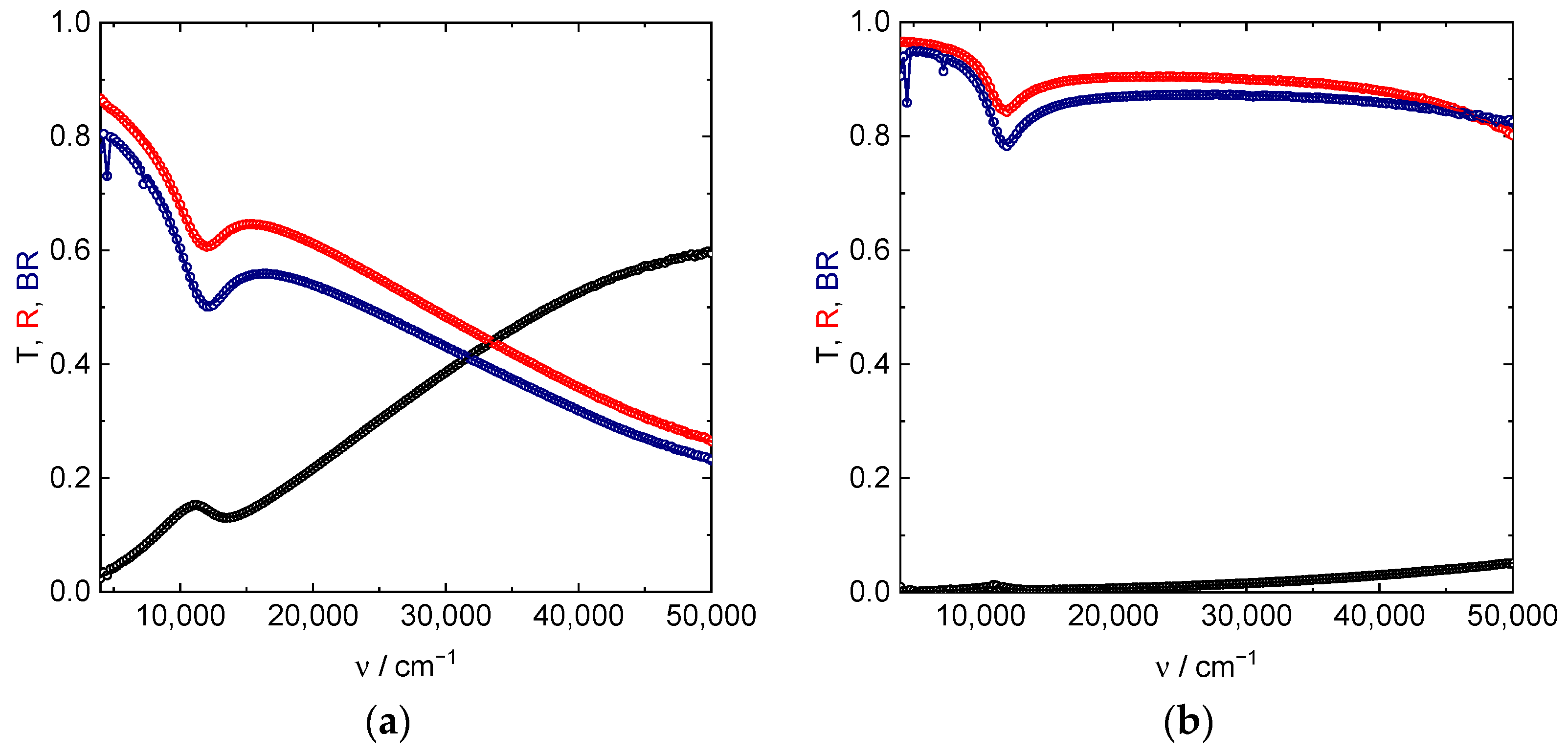
3.2.1. Spectrophotometry
3.2.2. X-ray Reflection (XRR)
3.2.3. Atomic Force Microscopy (AFM)
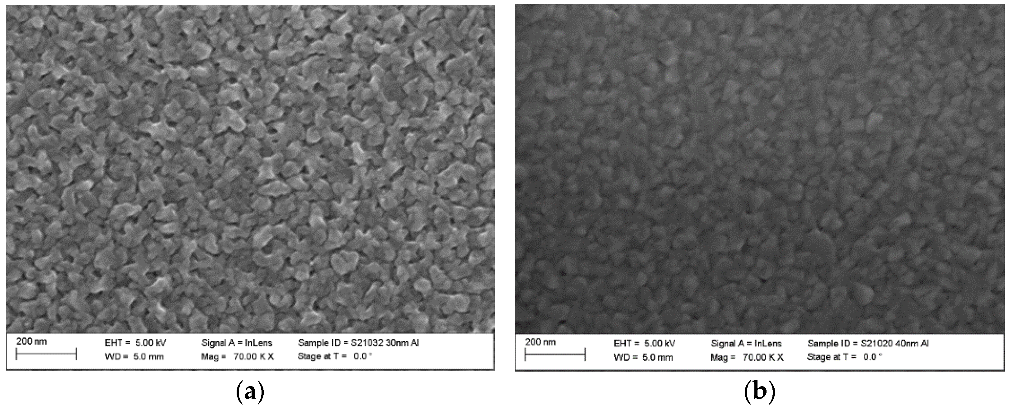
3.2.4. Scanning Electron Microscopy (SEM)
4. Results
4.1. Non-Optical Properties
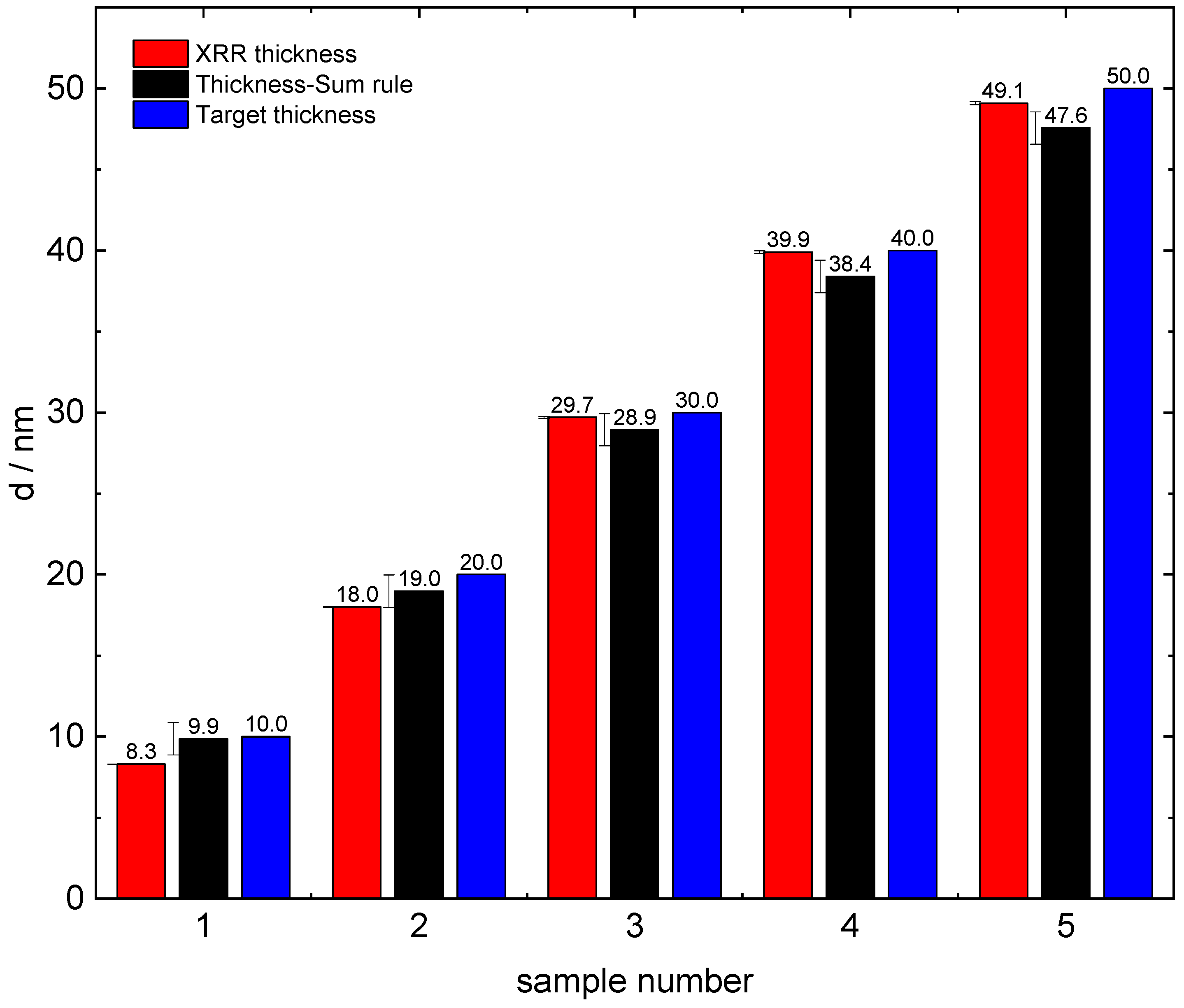
4.1.1. Film thickness
- i
- Quartz crystal monitoring data during deposition (electron beam evaporation only);
- ii
- X-ray reflection (XRR) analysis;
- iii
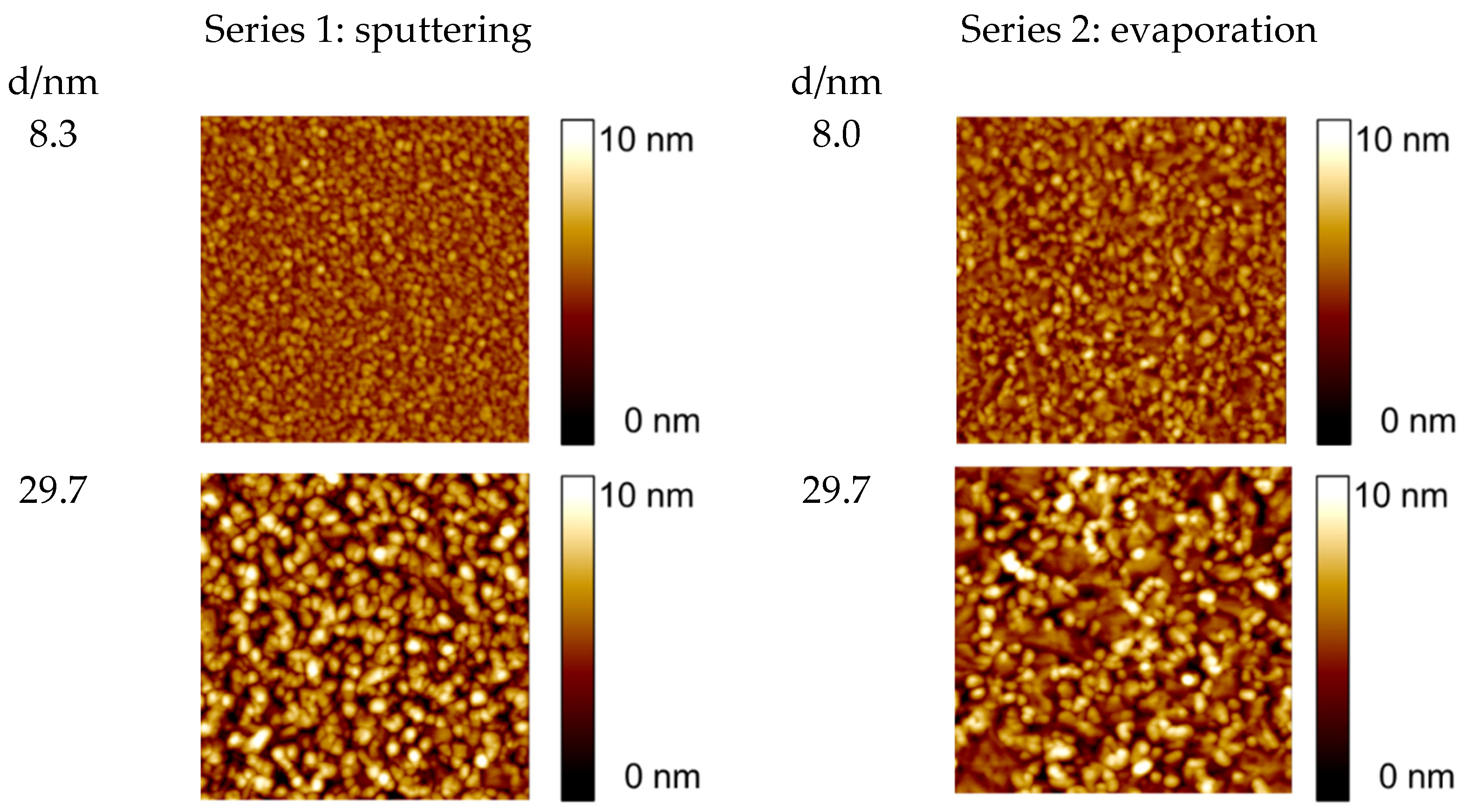
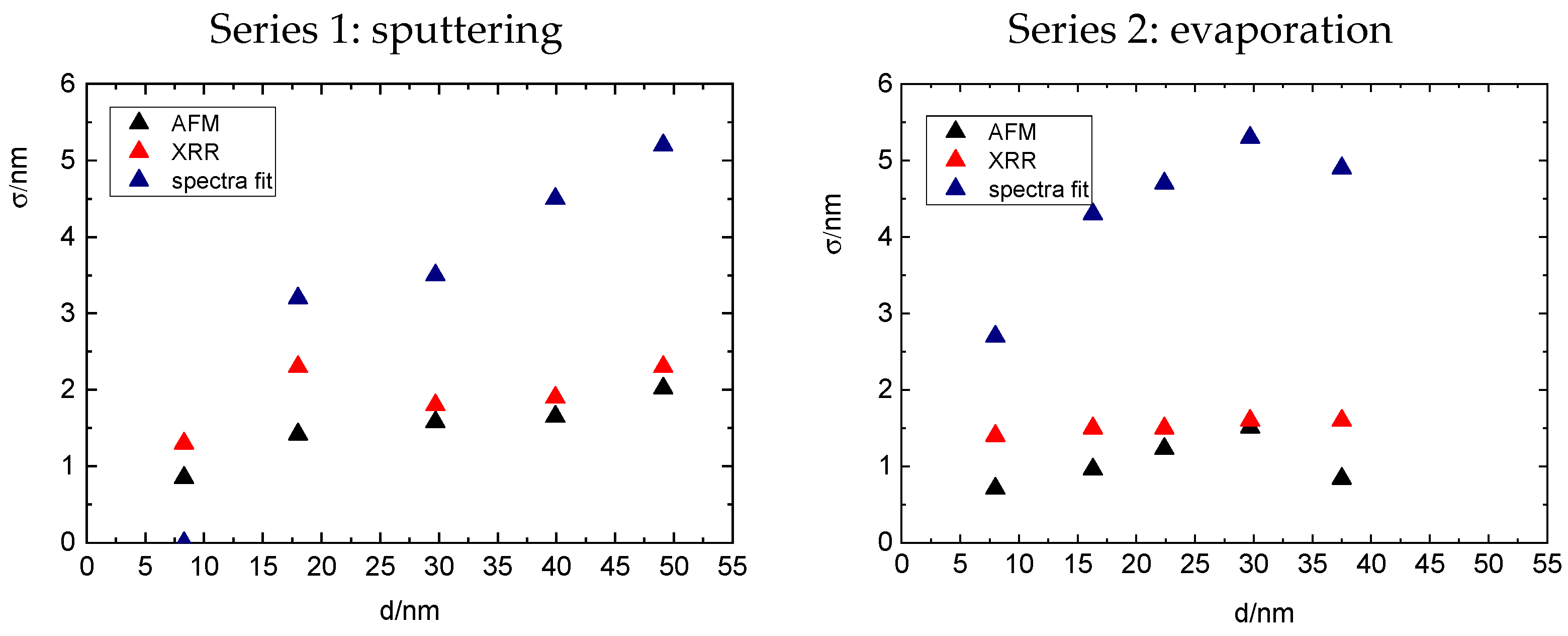
4.1.2. Surface Topology
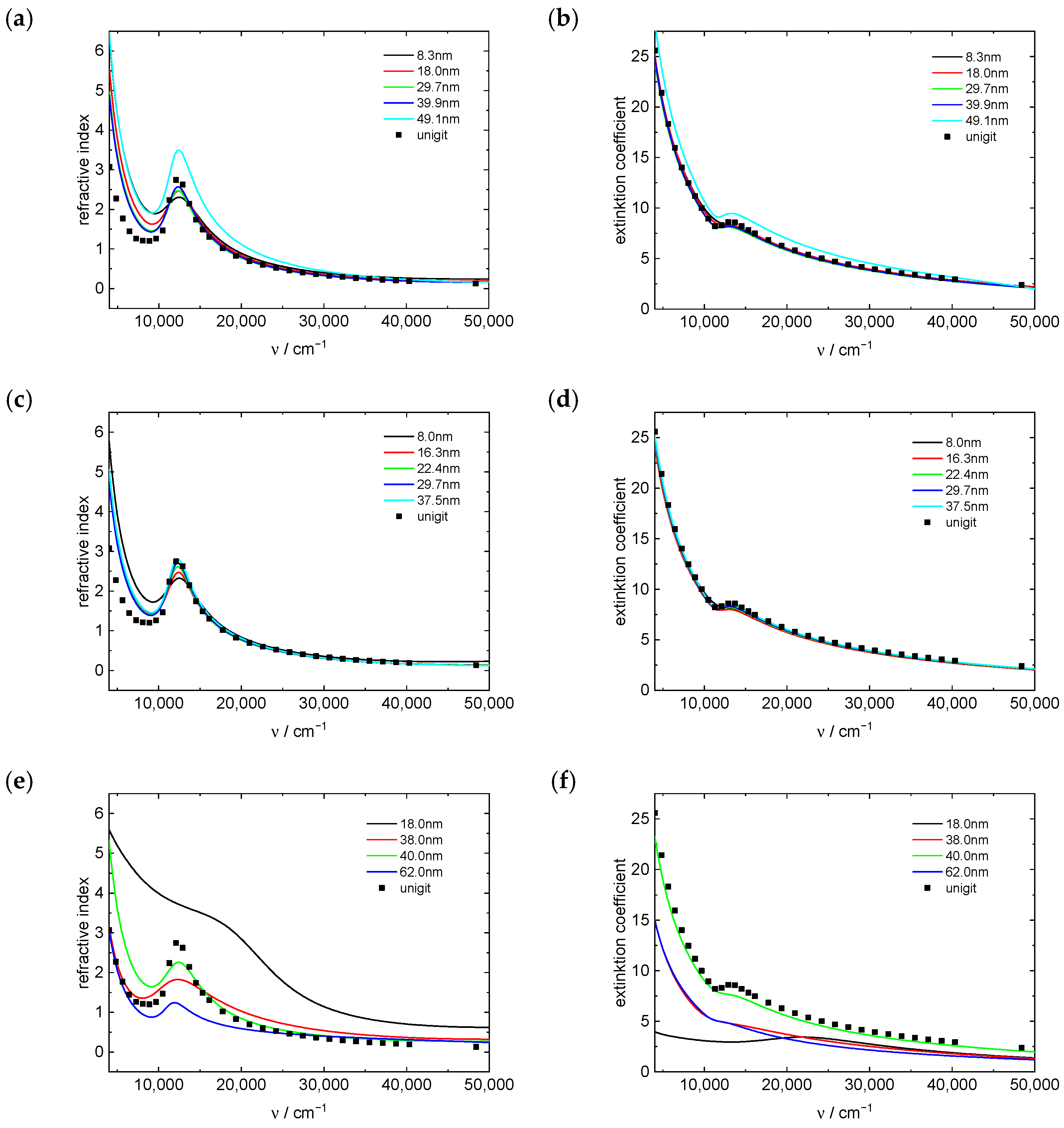
4.2. Optical Properties
5. Discussion
6. Summary and Outlook
Author Contributions
Funding
Institutional Review Board Statement
Informed Consent Statement
Data Availability Statement
Acknowledgments
Conflicts of Interest
References
- Hass, G. Filmed surfaces for reflecting optics. J. Opt. Soc. Am. 1955, 45, 945–952. [Google Scholar] [CrossRef]
- Gutiérrez-Luna, N.; Perea-Abarca, B.; Espinosa-Yáñez, L.; Honrado-Benítez, C.; de Lis, T.; Rodríguez-de Marcos, L.V.; Aznárez, J.A.; Larruquert, J.I. Temperature Dependence of AlF3 Protection on Far-UV Al Mirrors. Coatings 2019, 9, 428. [Google Scholar] [CrossRef]
- Wilbrandt, S.; Stenzel, O.; Nakamura, H.; Wulff-Molder, D.; Duparré, A.; Kaiser, N. Protected and enhanced aluminum mirrors for the VUV. Appl. Opt. 2014, 53, A125–A130. [Google Scholar] [CrossRef]
- Gläser, H.J. Dünnfilmtechnologie auf Flachglas; Hofmann-Verlag GmbH & Co., KG: Schorndorf, Germany, 1999; pp. 164–248. [Google Scholar]
- Willey, R.R. Practical Production of Optical Thin Films, 4th ed.; Lulu.com: Morrisville, NC, USA, 2017. [Google Scholar]
- Uhlig, H.; Stöckl, W.; Scheler, M. Electron Beam Vaporizer, Used for Vaporizing Aluminum, Comprises High Temperature Container Made of Electrically-Conducting Ceramic for Receiving Vaporized Material Inserted into Liquid-Cooled Crucible. German Patent Application DE 199 55 428 A 1, 18 November 1999. [Google Scholar]
- Ehrenreich, H.; Philipp, H.R.; Segall, B. Optical Properties of Aluminum. Phys. Rev. 1963, 132, 1918–1928. [Google Scholar] [CrossRef]
- Ordal, M.A.; Long, L.L.; Bell, R.J.; Bell, S.E.; Bell, R.R.; Alexander, R.W.; Ward, C.A. Optical properties of the metals Al, Co, Cu, Au, Fe, Pb, Ni, Pd, Pt, Ag, Ti, and W in the infrared and far infrared. Appl. Opt. 1983, 22, 1099–1119. [Google Scholar] [CrossRef] [PubMed]
- Rakić, A.D. Algorithm for the determination of intrinsic optical constants of metal films: Application to aluminum. Appl. Opt. 1995, 34, 4755–4767. [Google Scholar] [CrossRef]
- Schmitt, P.; Stempfhuber, S.; Felde, N.; Szeghalmi, A.V.; Kaiser, N.; Tünnermann, A.; Schwinde, S. Influence of seed layers on the reflectance of sputtered aluminum thin films. Opt. Express 2021, 29, 19472–19485. [Google Scholar] [CrossRef]
- Stempfhuber, S.; Felde, N.; Schwinde, S.; Trost, M.; Schenk, P.; Schröder, S.; Tünnermann, A. Influence of seed layers on optical properties of aluminum in the UV range. Opt. Express 2020, 28, 20324–20333. [Google Scholar] [CrossRef]
- Unigit Grating Solver Software. Available online: https://www.unigit.net (accessed on 24 August 2022).
- Macleod, H.A. Thin-Film Optical Filters, 4th ed.; CRC Press: Boca Raton, FL, USA, 2010. [Google Scholar]
- Willey, R.R.; Goldstein, F.T. Designing with Very Thin Optical Films. In Proceedings of the OSA Technical Digest of Optical Interference Coatings (OIC) Conference, Santa Ana Pueblo, NM, USA, 2–7 June 2019. Paper TC.5. [Google Scholar] [CrossRef]
- Rumsby, P.; Baloukas, B.; Zabeida, O.; Martinu, L. Continuous ultra-thin silver films obtained by a two-step method for improved control of the optical and microstructural characteristics. In Proceedings of the OSA Technical Digest of Optical Interference Coatings (OIC) Conference, Vancouver, BC, Canada, 19–24 June 2022. [Google Scholar]
- Moreau, A.; Shurvinton, R.; Morati, N.; Lemarchand, F.; Eles, B.; Destouches, N.; Lumeau, J. Development and applications of ultra-thin metallic films fabricated by Physical Vapor Deposition. In Proceedings of the OSA Technical Digest of Optical Interference Coatings (OIC) Conference, Vancouver, BC, Canada, 19–24 June 2022. [Google Scholar]
- Sytchkova, A.; Belosludtsev, A.; Volosevičienė, L.; Juškėnas, R.; Simniškis, R. Optical, structural and electrical properties of sputtered ultrathin chromium films. Opt. Mater. 2021, 121, 111530. [Google Scholar] [CrossRef]
- Gäbler, J.; Stenzel, O.; Wilbrandt, S.; Kaiser, N. Optische in-situ Prozessverfolgung und -steuerung des Aufdampfens optischer Beschichtungen durch gleichzeitige Messungen des Transmissions- und Reflexionsvermögens der wachsenden Schicht. Vak. Forsch. Und Prax. 2013, 25, 22–26. [Google Scholar] [CrossRef]
- Stenzel, O. Optical Coatings: Material Aspects in Theory and Practice; Springer: Berlin/Heidelberg, Germany, 2014; pp. 307–311. [Google Scholar]
- Du, H.; Xiao, J.Q.; Zou, Y.S.; Wang, T.G.; Gong, J.; Sun, C.; Wen, L.S. Optical properties of ultrathin aluminum films deposited by magnetron sputtering in visible band. Opt. Mater. 2006, 28, 944–949. [Google Scholar] [CrossRef]
- Stenzel, O.; Wilbrandt, S.; Stempfhuber, S.; Gäbler, D.; Wolleb, S.J. Spectrophotometric Characterization of Thin Copper and Gold Films Prepared by Electron Beam Evaporation: Thickness Dependence of the Drude Damping Parameter. Coatings 2019, 9, 181. [Google Scholar] [CrossRef]
- Kreibig, U. Optics of Nanosized metals. In Handbook of Optical Properties II: Optics of Small Particles, Interfaces, and Surfaces; Hummel, R.E., Wißmann, P., Eds.; CRC Press Inc.: Boca Raton, FL, USA, 1997; pp. 145–190. [Google Scholar]
- Held, M.; Stenzel, O.; Wilbrandt, S.; Kaiser, N.; Tünnermann, A. Manufacture and characterization of optical coatings with incorporated copper island films. Appl. Opt. 2012, 51, 4436–4447. [Google Scholar] [CrossRef]
- Amotchkina, T.V.; Janicki, V.; Sancho-Parramon, J.; Tikhonravov, A.V.; Trubetskov, M.K.; Zorc, H. General approach to reliable characterization of thin metal films. Appl. Opt. 2011, 50, 1453–1464. [Google Scholar] [CrossRef]
- Belosludtsev, A.; Sytchkova, A.; Kyžasa, N.; Bitinaitis, I.; Simniškis, R.; Drazdys, R. Ultrathin sputtered silver films protected by ALD alumina: Comparison of in-situ investigation with ex-situ resistance and ellipsometric measurements. Vacuum 2022, 195, 110669. [Google Scholar] [CrossRef]
- Ordal, M.A.; Bell, R.J.; Alexander, R.W.; Long, L.L.; Querry, M.R. Optical properties of fourteen metals in the infrared and far infrared: Al, Co, Cu, Au, Fe, Pb, Mo, Ni, Pd, Pt, Ag, Ti, V, and W. Appl. Opt. 1985, 24, 4493–4499. [Google Scholar] [CrossRef] [PubMed]
- Born, M.; Wolf, E. Principles of Optics; Pergamon Press: Oxford, UK, 1968. [Google Scholar]
- Dobrowolski, J.H.; Ho, F.C.; Waldorf, A. Determination of optical constants of thin film coating materials based on inverse synthesis. Appl. Opt. 1983, 22, 3191–3200. [Google Scholar] [CrossRef]
- Wilbrandt, S.; Stenzel, O. Empirical extension to the multioscillator model: The beta-distributed oscillator model. Appl. Opt. 2017, 56, 9892–9899. [Google Scholar] [CrossRef]
- Stenzel, O.; Wilbrandt, S. Beta-distributed oscillator model as an empirical extension to the Lorentzian oscillator model: Physical interpretation of the β_do model parameters. Appl. Opt. 2019, 58, 9318–9325. [Google Scholar] [CrossRef]
- Stenzel, O. The Physics of Thin Film Optical Spectra: An Introduction, 2nd ed.; Springer: Cham, Switzerland, 2016; pp. 25–39. [Google Scholar]
- Gall, D. Electron mean free path in elemental metals. J. Appl. Phys. 2016, 119, 085101. [Google Scholar] [CrossRef]
- Orosco, J.; Coimbra, C.F.M. On a causal dispersion model for the optical properties of metals. Appl. Opt. 2018, 57, 5333–5347. [Google Scholar] [CrossRef] [PubMed]
- Zeman, E.J.; Schatz, G.C. An accurate electromagnetic theory study of surface enhancement factors for silver, gold, copper, lithium, sodium, aluminum, gallium, indium, zinc, and cadmium. J. Phys. Chem. 1987, 91, 634–643. [Google Scholar] [CrossRef]
- Anderson, J.C. Conduction in thin semiconductor films. Adv. Phys. 1970, 79, 311–338. [Google Scholar] [CrossRef]
- Weißmantel, C.; Hamann, C. Grundlagen der Festkörperphysik; Springer: Berlin, Germany, 1979; pp. 413–416. [Google Scholar]
- DIN EN ISO 25178-2:2012; Geometrical Product Specifications (GPS)—Surface Texture: Areal—Part 2: Terms, Definitions and Surface Texture Parameters. Beuth Verlag: Berlin, Germany, 2012. [CrossRef]
- American Society of Mechanical Engineers. Surface Texture (Surface Roughness, Waviness and Lay): ASME B46.1-2002; ASME: New York, NY, USA, 2002. [Google Scholar]
- Duparré, A.; Ferre-Borrull, J.; Gliech, S.; Notni, G.; Steinert, J.; Bennett, J.M. Surface characterization techniques for determining the root-mean-square roughness and power spectral densities of optical components. Appl. Opt. 2002, 41, 154–171. [Google Scholar] [CrossRef] [PubMed]
- Schröder, S.; Herffurth, T.; Trost, M.; Duparré, A. Angle- resolved scattering and reflectance of extreme-ultraviolet multilayer coatings: Measurement and analysis. Appl. Opt. 2010, 49, 1503–1512. [Google Scholar] [CrossRef]
- Stenzel, O.; Macleod, A. Metal-dielectric composite optical coatings: Underlying physics, main models, characterization, design and application aspects. Adv. Opt. Technol. 2012, 1, 463–481. [Google Scholar] [CrossRef]
- Tikhonravov, A.V.; Trubetskov, M.K.; Tikhonravov, A.A.; Duparré, A. Effects of interface roughness on the spectral properties of thin films and multilayers. Appl. Opt. 2003, 42, 5140–5148. [Google Scholar] [CrossRef]
- Gross, R.; Marx, A. Festkörperphysik, 2nd ed.; de Gruyter: Berlin, Germany, 2014; pp. 301–303. [Google Scholar]
- French, R.H.; Müllejans, H.; Jones, D.J. Optical properties of aluminium oxide: Determined from vacuum ultraviolet and electron energy-loss spectroscopies. J. Am. Ceram. Soc. 1998, 81, 2549–2557. [Google Scholar] [CrossRef]
- Edmends, J.S.; Maldé, C.N.; Corrigan, S.J.B. Measurements of the far ultraviolet reflectivity of evaporated aluminium films under exposure to O2, H2O, CO and CO2. Vacuum 1990, 40, 471–475. [Google Scholar] [CrossRef]
- He, J.Y. Modelling UV and VUV Optical Losses of Rough Aluminum Films. Master’s Thesis, Friedrich Schiller University Jena, Abbe School of Photonics, Jena, Germany, 23 June 2022. [Google Scholar]
- Wilbrandt, S.; Petrich, R.; Stenzel, O. Optical interference coating characterization using neural networks. Proc. SPIE 1999, 3738, 517–528. [Google Scholar] [CrossRef]


| Reference | ||
|---|---|---|
| [7] | 102,400 | 518 |
| [26] | 119,000 | 330 |
| [33] | 120,800 | 165 |
| [34] | 97,100 | 519 |
| Process Sequence | Parameters for Series 1 | |
|---|---|---|
| Vacuum Pumping | Base Pressure | <5 × 10⁻⁶ mbar |
| Plasma pre-treatment | duration | ~60 s |
| power | 100 W | |
| gas flow Ar | 35 sccm | |
| gas flow O2 | 0 sccm | |
| Aluminum deposition | process pressure | ~1.5 × 10⁻⁶ mbar |
| power | 500 W | |
| gas flow Ar | 10 sccm | |
| dynamic deposition rate | 11.7 nm m/min | |
| Process Sequence | Parameters for Series 2 | Parameters for Series 3 | |
|---|---|---|---|
| Vacuum Pumping | Base Pressure | <5 × 10⁻⁶ mbar | |
| Plasma pre-treatment | duration | 180 s | |
| APS BIAS Voltage | 125 V | 140 V | |
| gas flow Ar | 12 sccm | ||
| gas flow O2 | 0 sccm | 0–10 sccm | |
| Aluminum deposition | deposition rate | 2–3 nm/s | ~0.1 nm/s |
| substrate temperature | room temperature | 120 °C | |
| APS Bias Voltage | 0 | 120 V | |
| gas flow Ar | 0 sccm | 12 sccm | |
| gas flow O2 | 0 sccm | 0 sccm | |
| Deposition Method | Al | AlxOy | Al | AlxOy | Al | AlxOy |
|---|---|---|---|---|---|---|
| d/nm | σ/nm | ρ/(g·cm−3) | ||||
| Sputtering Series 1 | 8.3 | 3.1 | 1.1 | 1.3 | 2.6989 | 3.9836 |
| 18.0 | 2.1 | 1.4 | 2.3 | |||
| 29.7 | 1.0 | 1.2 | 1.8 | |||
| 39.9 | 1.4 | 1.0 | 1.9 | |||
| 49.1 | 1.5 | 1.2 | 2.3 | |||
| Evaporation Series 2 | 8.0 | 1.9 | 1.0 | 1.4 | 2.6989 | 3.9836 |
| 16.3 | 1.2 | 2.1 | 1.5 | |||
| 22.4 | 1.2 | 2.0 | 1.5 | |||
| 29.7 | 1.0 | 1.6 | 1.6 | |||
| 37.5 | 1.1 | 2.0 | 1.6 | |||
| Assisted Evaporation Series 3 | 18 | - | 2.8 | - | 2.85 | - |
| 38 | 3.8 | |||||
| 40 | 3.3 | |||||
| 62 | 7.0 | 2.75 | ||||
| Dispersion Model Contribution: | 8.3 | 18.0 | 29.7 | 39.9 | 49.1 | |
|---|---|---|---|---|---|---|
| Drude Equation (4) | /cm−1 | 110,124 | 108,923 | 105,132 | 106,123 | 123,834 |
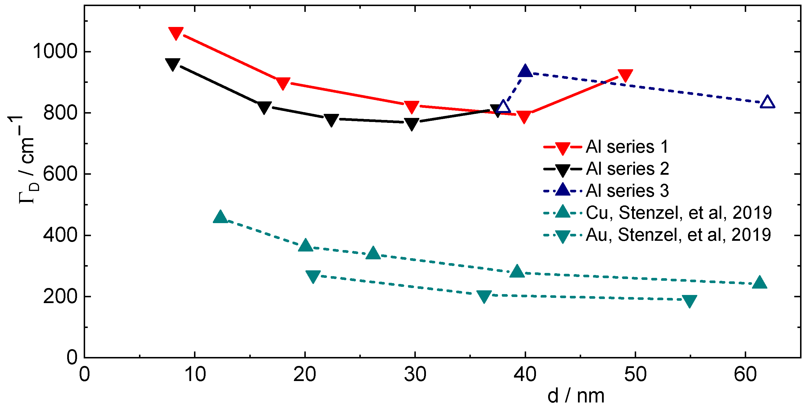
| /cm−1 | 1064.4 | 901.3 | 823.9 | 791.5 | 927.1 | |
| β_do Equation (3) | /cm−1 | 12,066 | 11,870 | 11,564 | 11,565 | 11,292 |
| /cm−1 | 131,106 | 202,425 | 443,938 | 461,171 | 919,485 | |
| /cm−1 | 305,720 | 296,174 | 276,788 | 290,959 | 455,017 | |
| /cm−1 | 2712.5 | 2003.6 | 1727.6 | 1687.7 | 1579.9 | |
| 0.000 | 0.082 | 0.001 | 0.000 | 0.000 | ||
| 7.766 | 14.472 | 27.948 | 28.904 | 65.992 | ||
| Lorentzian Equation (2) | /cm−1 | 65,000 | 65,000 | 65,000 | 65,000 | 65,000 |
| /cm−1 | 68,088 | 39,644 | 27,219 | 29,447 | 130,803 | |
| /cm−1 | 31,039 | 18,509 | 11,909 | 7800 | 90 | |
| /nm | 0.0 | 0.0 | 0.0 | 0.0 | 0.0 | |
| /nm | 2.7 | 0.0 | 3.2 | 3.5 | 4.5 | |
| /nm | 1.9 | 3.1 | 2.1 | 1.0 | 1.4 |
| Dispersion Model Contribution: | 8.0 | 16.3 | 22.4 | 29.7 | 37.5 | |
|---|---|---|---|---|---|---|
| Drude Equation (4) | /cm−1 | 107,397 | 103,963 | 105,581 | 106,440 | 108,328 |
| /cm−1 | 963.4 | 822.3 | 781.2 | 767.5 | 811.8 | |
| β_do Equation (3) | /cm−1 | 12,165 | 12,055 | 11,982 | 11,941 | 11,881 |
| /cm−1 | 37,246 | 43,681 | 49,097 | 62,348 | 93,918 | |
| /cm−1 | 283,115 | 263,706 | 274,932 | 284,404 | 293,826 | |
| /cm−1 | 2446.7 | 1811.7 | 1638.2 | 1546.6 | 1480.1 | |
| 0.122 | 0.176 | 0.199 | 0.214 | 0.225 | ||
| 3.350 | 3.879 | 4.454 | 5.652 | 8.727 | ||
| Lorentzian Equation (2) | /cm−1 | 65,000 | 65,000 | 65,000 | 65,000 | 65,000 |
| /cm−1 | 117,565 | 234,658 | 143,772 | 230,593 | 1,057,703 | |
| /cm−1 | 44,812 | 112,896 | 88,830 | 125,819 | 259,820 | |
| /nm | 0.0 | 0.0 | 0.0 | 0.0 | 0.0 | |
| /nm | 2.7 | 4.3 | 4.7 | 5.3 | 4.9 | |
| /nm | 1.9 | 1.2 | 1.2 | 1.0 | 1.1 |
| Dispersion Model Contribution: | 18.0 | 38.0 | 40.0 | 62.0 | |
|---|---|---|---|---|---|
| Drude Equation (4) | /cm−1 | 48,902 | 65,374 | 101,313 | 64,280 |
| /cm−1 | 8914.9 | 815.8 | 932.3 | 831.1 | |
| β_do Equation (3) | /cm−1 | 2224 | 10,360 | 11,932 | 11,336 |
| /cm−1 | 18,127 | 1,032,317 | 148,323 | 58,417 | |
| /cm−1 | 841,157 | 262,484 | 283,329 | 115,795 | |
| /cm−1 | 6826.0 | 3860.7 | 2465.8 | 1675.6 | |
| 0.000 | 0.044 | 0.010 | 0.316 | ||
| 0.091 | 57.076 | 7.880 | 1.790 | ||
| Lorentzian Equation (2) | /cm−1 | 65,000 | 65,000 | 65,000 | 65,000 |
| /cm−1 | 127,847 | 43,810 | 214,250 | 3262 | |
| /cm−1 | 45,019 | 32,507 | 78,407 | 1,295,243 | |
| /nm | 0.0 | 0.0 | 0.0 | 0.0 | |
| /nm | 0.0 | 6.3 | 6.1 | 25.7 | |
| /nm | 1.6 | 1.6 | 1.6 | 1.6 |
| Preparation Method | |||
|---|---|---|---|
| “rule of thumb” | broadens the NIR spectral feature | enhances IR reflectance | enhances UV reflectance |
| sputtering | 1727.6 | 823.9 | 105,132 |
| evaporation | 1546.6 | 767.5 | 106,440 |
Publisher’s Note: MDPI stays neutral with regard to jurisdictional claims in published maps and institutional affiliations. |
© 2022 by the authors. Licensee MDPI, Basel, Switzerland. This article is an open access article distributed under the terms and conditions of the Creative Commons Attribution (CC BY) license (https://creativecommons.org/licenses/by/4.0/).
Share and Cite
Wilbrandt, S.; Stenzel, O.; Liaf, A.; Munzert, P.; Schwinde, S.; Stempfhuber, S.; Felde, N.; Trost, M.; Seifert, T.; Schröder, S. Spectrophotometric Characterization of Thin Semi-Transparent Aluminum Films Prepared by Electron Beam Evaporation and Magnetron Sputtering. Coatings 2022, 12, 1278. https://doi.org/10.3390/coatings12091278
Wilbrandt S, Stenzel O, Liaf A, Munzert P, Schwinde S, Stempfhuber S, Felde N, Trost M, Seifert T, Schröder S. Spectrophotometric Characterization of Thin Semi-Transparent Aluminum Films Prepared by Electron Beam Evaporation and Magnetron Sputtering. Coatings. 2022; 12(9):1278. https://doi.org/10.3390/coatings12091278
Chicago/Turabian StyleWilbrandt, Steffen, Olaf Stenzel, Abrar Liaf, Peter Munzert, Stefan Schwinde, Sven Stempfhuber, Nadja Felde, Marcus Trost, Tina Seifert, and Sven Schröder. 2022. "Spectrophotometric Characterization of Thin Semi-Transparent Aluminum Films Prepared by Electron Beam Evaporation and Magnetron Sputtering" Coatings 12, no. 9: 1278. https://doi.org/10.3390/coatings12091278