
Spectroscopic Analysis of CF4/O2 Plasma Mixed with N2 for Si3N4 Dry Etching


Abstract
:1. Introduction
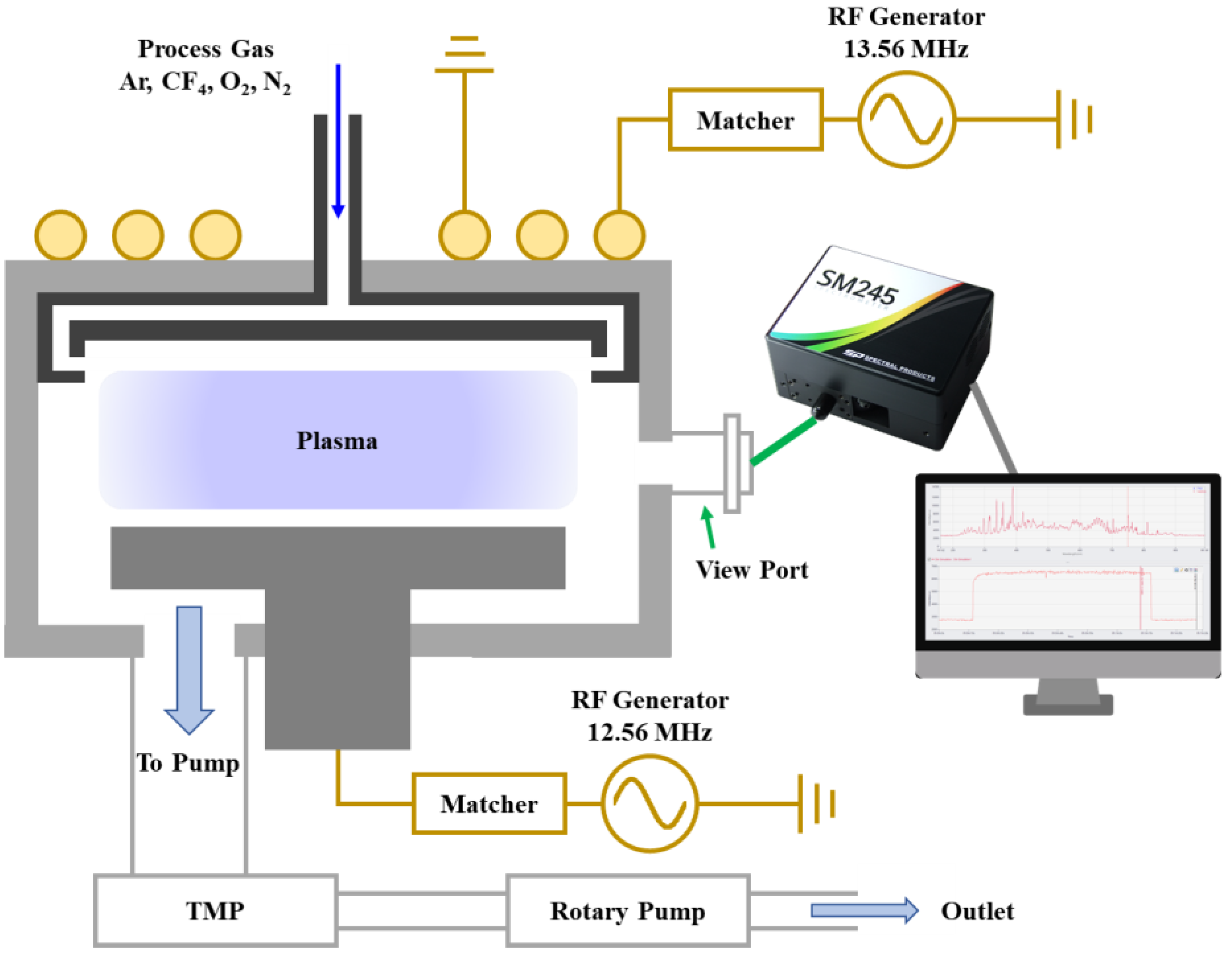
2. Experiment
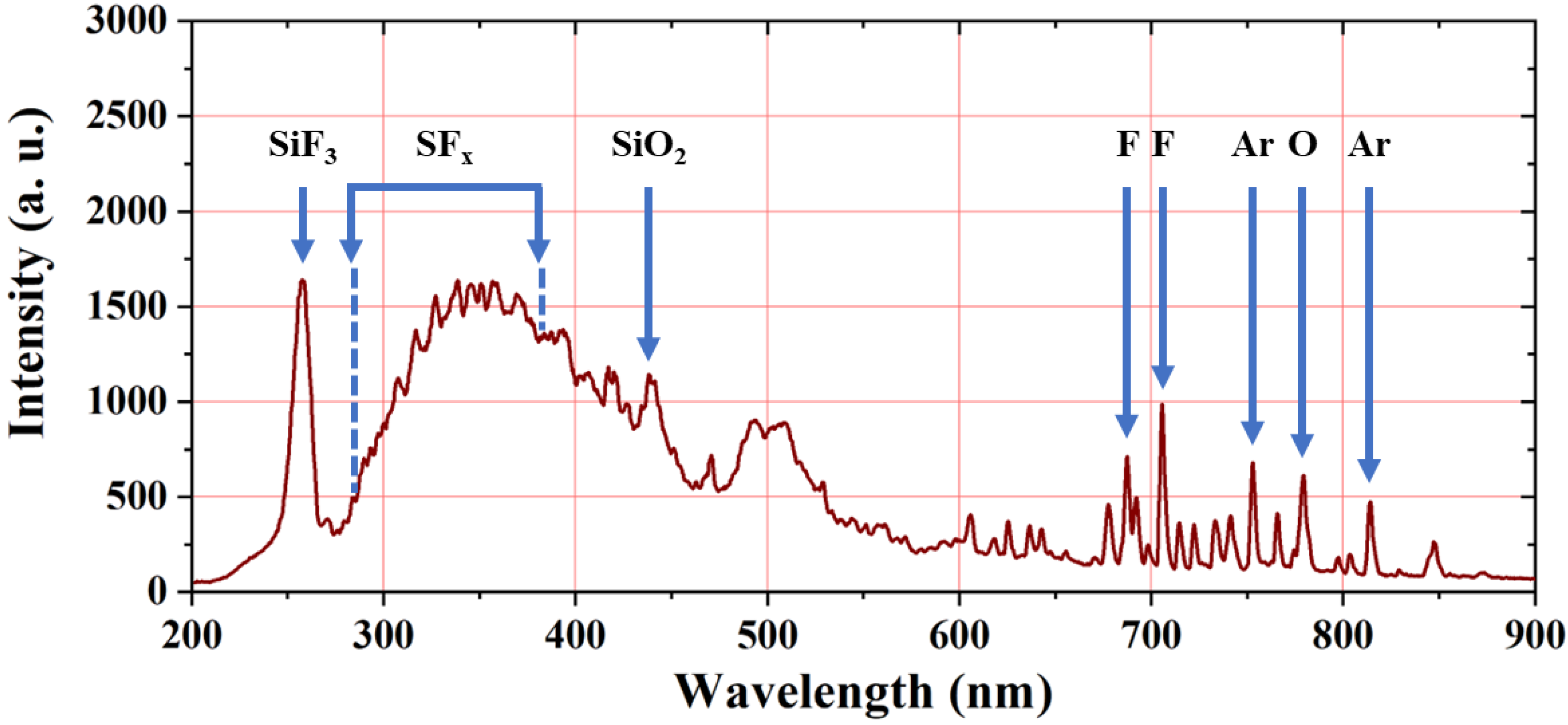
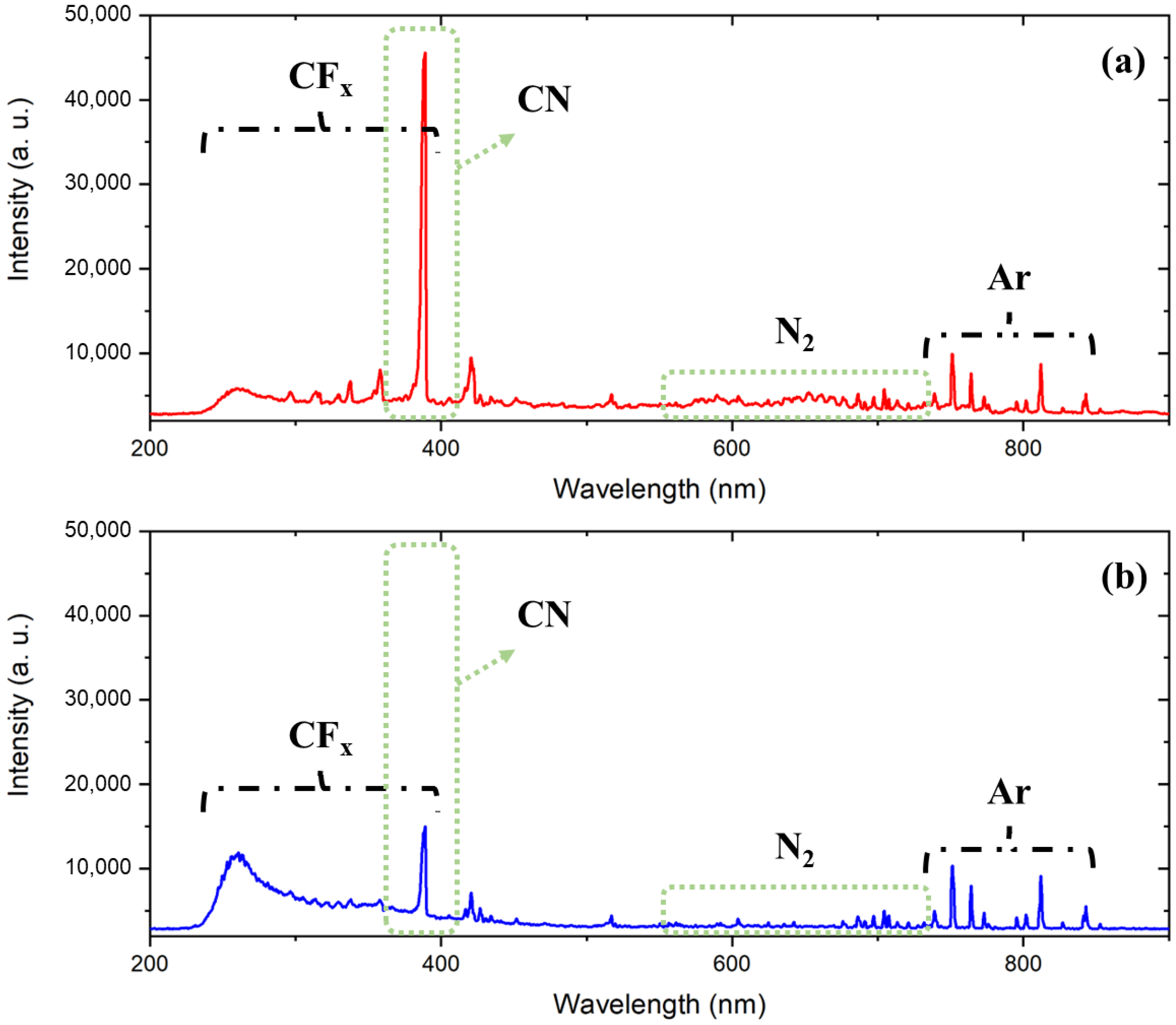
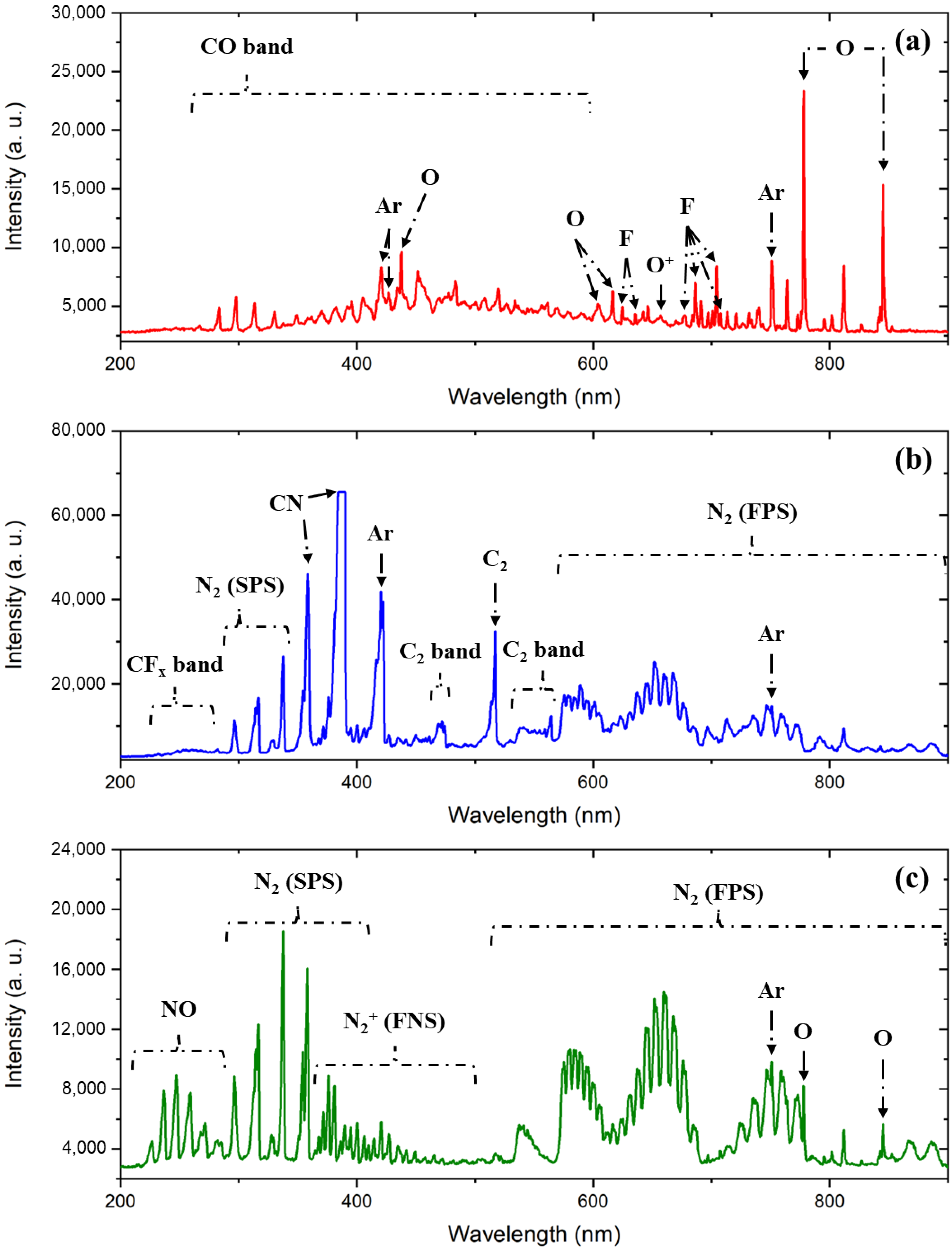
3. Results and Discussion
4. Conclusions
Author Contributions
Funding
Institutional Review Board Statement
Informed Consent Statement
Data Availability Statement
Acknowledgments
Conflicts of Interest
References
- Arienzo, M.; Orr-Arienzo, W.A. Silicon Nitride in Semiconductor Device Technology. In Materials Science Forum; Trans Tech Publication, Ltd.: Bäch, Switzerland, 1991; Volume 47, pp. 228–248. [Google Scholar] [CrossRef]
- Kim, B.; Hong, S.J. In-Situ Virtual Metrology for the Silicon-Dioxide Etch Rate by using Optical Emission Spectroscopy Data. J. Korean Phys. Soc. 2014, 65, 168–175. [Google Scholar] [CrossRef]
- Cheng, Y.; Lee, C.; Haung, C. Plasma Damage on Low-k Dielectric Materials. In Plasma Science and Technology-Basic Fundamentals and Modern Applications; IntechOpen: Vienna, Austria, 2018; Volume 15, pp. 291–318. [Google Scholar] [CrossRef] [Green Version]
- King, S.W.; French, M.; Bielefeld, J.; Lanford, W.A. Fourier Transform Infrared Spectroscopy Investigation of Chemical Bonding in Low-k a-SiC: H Thin Films. J. Non-Cryst. Solids 2011, 357, 2970–2983. [Google Scholar] [CrossRef]
- Wallace, R.M. In-Situ Studies of Interfacial Bonding of High-k Dielectrics for CMOS Beyond 22 nm. ECS Trans. 2008, 16, 255–271. [Google Scholar] [CrossRef]
- Cleveland, E.R.; Ruppalt, L.B.; Bennett, B.R.; Prokes, S.M. Effect of an In Situ Hydrogen Plasma Pre-Treatment on the Reduction of GaSb Native Oxides Prior to Atomic Layer Deposition. Appl. Surf. Sci. 2013, 277, 167–175. [Google Scholar] [CrossRef]
- Jang, J.; Kim, H.-S.; Cho, W.; Cho, H.; Kim, J.; Shim, S.I.; Jang, Y.; Jeong, J.-H.; Son, B.-K.; Kim, D.W.; et al. Vertical Cell Array Using TCAT (Terabit Cell Array Transistor) Technology for Ultra High Density NAND Flash Memory. In Proceedings of the Symposium on VLSI Technology, Kyoto, Japan, 15–17 June 2009. [Google Scholar]
- Choi, J.E.; Song, J.; Lee, Y.H.; Hong, S.J. Deep Neural Network Modeling of Multiple Oxide/Nitride Deposited Dielectric Films for 3D-NAND Flash. Appl. Sci. Converg. Technol. 2020, 29, 190–194. [Google Scholar] [CrossRef]
- Khan, A.H.; Srinivasan, S.; Choi, J.; Athayde, A.; Achutharaman, R. Etch Challenges for 3D NAND Flash Technology. In Proceedings of the ECS and SMEQ Joint International Meeting, Cancun, Mexico, 5–9 October 2014. [Google Scholar] [CrossRef]
- Clarke, P.E.; Field, D.; Hydes, A.J.; Klemperer, D.F.; Seakins, M.J. Mass Spectrometric Studies of Plasma Etching of Silicon Nitride. J. Vac. Sci. Technol. B Microelectron. Nanometer Struct. 1985, 3, 1614. [Google Scholar] [CrossRef]
- Field, D.; Klemperer, D.F.; Wade, I.T. Spectroscopic Studies of Fluorescent Emission in Plasma Etching of Silicon Nitride. J. Vac. Sci. Technol. B Microelectron. Process. Phenom. 1988, 6, 551. [Google Scholar] [CrossRef]
- Reyes-Betanzo, C.; Moshkalyov, S.A.; Swart, J.W.; Ramos, A. Silicon Nitride Etching in High- and Low-Density Plasmas using SF6/O2/N2 Mixtures. J. Vac. Sci. Technol. A Vac. Surf. Film 2003, 21, 461. [Google Scholar] [CrossRef] [Green Version]
- Barsukov, Y.; Volynets, V.; Lee, S.; Kim, G.; Lee, B.; Nam, S.K.; Han, K. Role of NO in Highly Selective SiN/SiO2 and SiN/Si Etching with NF3/O2 Remote Plasma: Experiment and Simulation. J. Vac. Sci. Technol. A Vac. Surf. Film 2017, 35, 061310. [Google Scholar] [CrossRef]
- Huang, S.; Volynets, V.; Hamilton, J.R.; Nam, S.K.; Song, I.; Lu, S.; Tennyson, J.; Kushner, M.J. Downstream Etching of Silicon Nitride using Continuous-Wave and Pulsed Remote Plasma Sources Sustained in Ar/NF3/O2 Mixtures. J. Vac. Sci. Technol. A Vac. Surf. Film 2018, 36, 021305. [Google Scholar] [CrossRef]
- Kuboi, N.; Tatsumi, T.; Kinoshita, T.; Shigetoshi, T.; Fukasawa, M.; Komachi, J.; Ansai, H. Prediction of Plasma-Induced Damage Distribution during Silicon Nitride Etching using Advanced Three-Dimensional Voxel Model. J. Vac. Sci. Technol. A Vac. Surf. Film 2015, 33, 061308. [Google Scholar] [CrossRef]
- Prévost, E.; Cunge, G.; De-Buttet, C.; Lagrasta, S.; Vallier, L.; Petit-Etienne, C. Study of selective chemical downstream plasma etching of silicon nitride and silicon oxide for advanced patterning applications. In Proceedings of the SPIE Advanced Lithography, San Jose, CA, USA, 26 February–2 March 2017. [Google Scholar] [CrossRef]
- Shinoda, K.; Miyoshi, N.; Kobayashi, H.; Izawa, M.; Saeki, T.; Ishikawa, K.; Hori, M. Self-Limiting Reactions of Ammonium Salt in CHF3/O2 Downstream Plasma for Thermal-Cyclic Atomic Layer Etching of Silicon Nitride. J. Vac. Sci. Technol. A Vac. Surf. Film 2019, 37, 051002. [Google Scholar] [CrossRef]
- Hsiao, S.N.; Nguyen, T.-T.-N.; Tsutsumi, T.; Ishikawa, K.; Sekine, M.; Hori, M. Etching Characteristics of PECVD-Prepared SiN Films with CF4/D2 and CF4/H2 Plasmas at Different Temperatures. In Proceedings of the 2020 International Symposium on Semiconductor Manufacturing (ISSM), Tokyo, Japan, 15–16 December 2020. [Google Scholar] [CrossRef]
- Hamada, T.; Masuda, S.; Nishida, K.; Yamamoto, S. Etching Characteristics of SixNy Film on Textured Single Crystalline Silicon Surface using Ar/CF4 and He/CF4 Surface-Discharge Plasma. Coatings 2020, 10, 563. [Google Scholar] [CrossRef]
- Jang, D.B.; Hong, S.J. In-Situ Monitoring of Multiple Oxide/Nitride Dielectric Stack PECVD Deposition Process. Trans. Electr. Electron. Mater. 2018, 19, 21–26. [Google Scholar] [CrossRef]
- Jang, Y.; Roh, H.; Park, S.; Jeong, S.; Ryu, S.; Kwon, J.; Kim, N.; Kim, G. Characteristics of a Plasma Information Variable in Phenomenology-Based, Statistically-Tuned Virtual Metrology to Predict Silicon Dioxide Etching Depth. Curr. Appl. Phys. 2019, 19, 1068–1075. [Google Scholar] [CrossRef]
- Rachdi, L.; Hofmann, M. Use of Optical Emission Spectroscopy to Predict Silicon Nitride Layer Properties. Vacuum 2021, 191, 110322. [Google Scholar] [CrossRef]
- Zhu, X.; Pu, Y. Optical Emission Spectroscopy in Low-Temperature Plasmas Containing Argon and Nitrogen: Determination of the Electron Temperature and Density by the Line-Ratio Method. J. Phys. D 2010, 43, 403001. [Google Scholar] [CrossRef]
- Evdokimov, K.E.; Konischev, M.E.; Pichugin, V.F.; Sun, Z. Study of Argon Ions Density and Electron Temperature and Density in Magnetron Plasma by Optical Emission Spectroscopy and Collisional-Radiative Model. Res. Eff. Technol. 2017, 3, 187–193. [Google Scholar] [CrossRef]
- Onishi, H.; Yamazaki, F.; Hakozaki, Y.; Takemura, M.; Nezu, A.; Akatsuka, H. Measurement of Electron Temperature and Density of Atmospheric-Pressure Non-Equilibrium Argon Plasma Examined with Optical Emission Spectroscopy. Jpn. J. Appl. Phys. 2021, 60, 026002. [Google Scholar] [CrossRef]
- Chien, K.; Chang, C.; Djurdjanovic, D. Virtual Metrology Modeling of Reactive Ion Etching Based on Statistics-Based and Dynamics-Inspired Spectral Features. J. Vac. Sci. Technol. B Nanotechnol. Microelectron. Mater. Process. Meas. Phenom. 2021, 39, 064003. [Google Scholar] [CrossRef]
- Kim, W.J.; Bang, I.Y.; Kim, J.H.; Park, Y.S.; Kwon, H.T.; Shin, G.W.; Kang, M.; Cho, Y.; Kwon, B.; Kwak, J.H. Etching Characteristics of NF3 and F3NO at Reactive Ion Etching Plasma for Silicon Oxide and Silicon Nitride. J. Korean Phys. Soc. 2021, 79, 290–296. [Google Scholar] [CrossRef]
- Xu, D.; Zou, S.; Xin, Y.; Su, X.; Wang, X. Characteristics of Dual-Frequency Capacitively Coupled SF6/O2 Plasma and Plasma Texturing of Multi-Crystalline Silicon. Chin. Phys. B 2014, 23, 065201. [Google Scholar] [CrossRef]
- Duluard, C.Y.; Dussart, R.; Tillocher, T.; Pichon, L.E.; Lefaucheux, P.; Puech, M.; Ranson, P. SO2 Passivating Chemistry for Silicon Cryogenic Deep Etching. Plasma Sources Sci. Technol. 2008, 17, 045008. [Google Scholar] [CrossRef]
- Cruden, B.A.; Rao, M.; Sharma, S.P.; Meyyappan, M. Fourier-Transform Infrared and Optical Emission Spectroscopy of CF4/O2/Ar Mixtures in an Inductively Coupled Plasma. J. Appl. Phys. 2003, 93, 5053–5062. [Google Scholar] [CrossRef]
- Czerwiec, T.; Greer, F.; Graves, D.B. Nitrogen Dissociation in a Low Pressure Cylindrical ICP Discharge Studied by Actinometry and Mass Spectrometry. J. Phys. D 2005, 38, 4278. [Google Scholar] [CrossRef]
- Kawata, H.; Takao, Y.; Murata, K.; Nagami, K. Optical Emission Spectroscopy of CF4+O2 Plasmas using a New Technique. Plasma Chem. Plasma Process. 1988, 8, 189–206. [Google Scholar] [CrossRef]
- Kiss, L.; Nicolai, J.; Conner, W.T.; Sawin, H.H. CF and CF2 Actinometry in a CF4/Ar Plasma. J. Appl. Phys. 1992, 71, 3186–3192. [Google Scholar] [CrossRef]
- Jamroz, P.; Zyrnicki, W. Optical Emission Characteristics of Glow Discharge in the N2–H2–Sn(CH3)4 and N2–Ar–Sn(CH3)4 Mixtures. Surf. Coat. Technol. 2006, 201, 1444–1453. [Google Scholar] [CrossRef]
- Kimura, T.; Hanaki, K. Experiments and Global Model Analysis of Inductively Coupled CF4/O2/Ar Plasmas. Jpn. J. Appl. Phys. 2008, 47, 8537. [Google Scholar] [CrossRef]
- Li, J.; Kim, S.J.; Han, S.; Kim, Y.; Chae, H. Etching Characteristics of Hydrogenated Amorphous Carbon with Different sp2/sp3 Hybridization Ratios in CF4/O2 Plasmas. Plasma Process. Polym. 2021, 18, 2100075. [Google Scholar] [CrossRef]
- Ichikawa, Y.; Sakamoto, T.; Nezu, A.; Matsuura, H.; Akatsuka, H. Actinometry Measurement of Dissociation Degrees of Nitrogen and Oxygen in N2–O2 Microwave Discharge Plasma. Jpn. J. Appl. Phys. 2010, 49, 106101. [Google Scholar] [CrossRef]
- Kim, Y.S.; Jeon, S.H.; Jung, C.H. Fluorination Reaction of Uranium Dioxide in CF4/O2/N2 Rf Plasma. Ann. Nucl. Energy 2003, 30, 1199–1209. [Google Scholar] [CrossRef]
- Premachandran, V. Enhanced Etching of Silicon in CF4-O2-N2 Plasma. Appl. Phys. Lett. 1990, 57, 678–679. [Google Scholar] [CrossRef]


| No. | RF Power [W] | Pressure [mTorr] | Gas [sccm] | |||
|---|---|---|---|---|---|---|
| CF4 | O2 | N2 | Ar | |||
| 1 | 300 | 5 | 40 | 0 | 0 | 4 |
| 2 | 0 | 40 | 0 | |||
| 3 | 0 | 0 | 40 | |||
| 4 | 20 | 20 | 0 | |||
| 5 | 20 | 0 | 20 | |||
| 6 | 0 | 20 | 20 | |||
| 7 | 40 | 4 | 0 | |||
| 8 | 40 | 4 | 2 | |||
| 9 | 40 | 4 | 4 | |||
| 10 | 40 | 4 | 6 | |||
| 11 | 40 | 4 | 8 | |||
| Species | Wavelength (nm) | Shifted Wavelength (nm) |
|---|---|---|
| Ar | 750.4 | 750.87 |
| F | 712.8 | 713.1 |
| 703.7 | 704.1 | |
| 685.6 | 686.5 | |
| O | 844.6 | 845.08 |
| 777.1 | 778.01 | |
| NO | 259.2 | 259.07 |
| 247.9 | 247.42 | |
| N2 | 394.3 | 394.79 |
| 380.56 | 381.1 | |
| 337.1 | 337.62 | |
| CN | 388.43 | 388.92 |
| CO | 483.5 | 483.61 |
| 438 | 438.16 | |
| 297.7 | 297.73 | |
| 283 | 283.27 |
| Species | Shifted Wavelength (nm) | Transition | Threshold Energy (eV) |
|---|---|---|---|
| Ar | 750.87 | 3s23p5(2P°1/2)4p → 3s23p5(2P°1/2)4s | 13.5 |
| F | 704.1 | 2s22p4(3P)3p → 2s22p4(3P)3s | 14.7 |
| 686.5 | 2s22p4(3P)3p → 2s22p4(3P)3s | 14.5 | |
| O | 845.08 | 2s22p3(4S°)3p → 2s22p3(4S°)3s | 11 |
| 778.01 | 2s22p3(4S°)3p → 2s22p3(4S°)3s | 10.7 | |
| NO | 259.07 | A2Σ+ → X2Π (0,3) A2Σ+ → X2Π (0,2) | − |
| 247.42 | − | ||
| N2 | 394.79 | C3Πu → B3Πg (2,5) C3Πu → B3Πg (0,2) C3Πu → B3Πg (0,0) | − |
| 381.1 | − | ||
| 337.62 | − | ||
| CN | 388.92 | B2Σ → X2Σ (0,0) | − |
| CO | 483.61 | B1Σ → A1π (0,1) b3Σ+ → a3π (0,1) | − |
| 297.73 | |||
| 283.27 | b3Σ+ → a3π (0,0) | − |
| N2 Ejected | |||
|---|---|---|---|
| Production | Consumption | Production | Consumption |
| CF4 + E => CF3+ + F + 2E | F + E => F+ + 2E | CF4 + E => CF3+ + F + 2E | F + E => F+ + 2E |
| CF4 + E => CF2+ + 2F + 2E | F + F− => F2 + E | CF4 + E => CF3 + F + E | F + F− => F2 + E |
| CF4 + E => CF+ + F2 + F + 2E | F + O2− => O2 + F− | CF4 + E => 2F + CF2 + E | F + F− => 2F + E |
| CF4 + E => CF3 + F + E | F + CF3 => CF4 | CF4 + E => F2 + CF + F + E | F + CF3 => CF4 |
| CF4 + E => 2F + CF2 + E | F + CF2 => CF3 | CF3+ + E => CF2 + F | F + CF2 => CF3 |
| CF4 + E => F2 + CF + F + E | F + CF => CF2 | CF3 + E => CF2 + F + E | F + COF => COF2 |
| CF3+ + E => CF2 + F | F + COF => COF2 | CF2 + E => CF + F + E | |
| CF3 + E => CF2 + F + E | CF2 + E => CF+ + F + 2E | ||
| CF3 + E => CF2+ + F + 2E | F+ + E => F | ||
| CF2 + E => CF + F + E | F2 + E => F + F− | ||
| CF2 + E => CF+ + F + 2E | CF3+ + F− => 2F + CF2 | ||
| CF + E => C + F + E | CF+ + F− => CF + F | ||
| F+ + E => F | F2 + F− => F + F2 + E | ||
| F2 + E => F + F− | F+ + F− => 2F | ||
| CF3+ + F− => 2F + CF2 | CF3+ + F− => F + CF3 | ||
| CF+ + F− => CF + F | F+ + C => C+ + F | ||
| F + F− => 2F + E | CF+ + F− => 2F + C | ||
| F2 + F− => F + F2 + E | F2 + CF2 => CF3 + F | ||
| F+ + F− => 2F | F2 + CF3 => CF4 + F | ||
| F3+ + F− => F + CF3 | CF+ + E => C + F | ||
| F+ + C => C+ + F | O + F− => F + O + E | ||
| CF+ + F− => 2F + C | F+ + O => O+ + F | ||
| F2 + CF2 => CF3 + F | FO + O => O2 + F | ||
| F2 + CF3 => CF4 + F | O + CF2 => COF + F | ||
| CF+ + E => C + F | O + CF2 => 2F + CO | ||
| O2+ + CF4 => CF3+ + O2 + F | O + CF3 => COF2 + F | ||
| O + F− => F + O + E | O + COF => CO2 + F | ||
| F+ + O => O+ + F | O* + CF3 => COF2 + F | ||
| F+ + O2 => O2+ + F | O* + CF2 => COF + F | ||
| FO + O => O2 + F | O* + CF2 => 2F + CO | ||
| O + CF => CO + F | O* + COF => CO2 + F | ||
| O + CF2 => COF + F | O* + FO => O2 + F | ||
| O + CF2 => 2F + CO | COF + E => CO + F + E | ||
| O + CF3 => COF2 + F | C+ + F− => F + C | ||
| O + COF => CO2 + F | CF2+ + F− => F + CF2 | ||
| O* + CF => CO + F | O2+ + CF4 => CF3+ + O2 + F | ||
| O* + CF3 => COF2 + F | F+ + O2 => O2+ + F | ||
| O* + CF2 => COF + F | CF3 + E => CF2+ + F + 2E | ||
| O* + CF2 => 2F + CO | |||
| O* + COF => CO2 + F | |||
| O* + FO => O2 + F | |||
| COF + E => CO + F + E | |||
| CF + N => CN + F | |||
| CF2 + N => 2F + CN | |||
| CF3 + N => F2 + CN + F | |||
| N+ + F− => F + N | |||
| N2+ + F− => F + N2 | |||
| C+ + F− => F + C | |||
| CF2+ + F− => F + CF2 | |||
| Reaction | Comment |
|---|---|
| F + SiN(s) → SiNF(s) | Fluorination |
| F + SiNF(s) → SiNF2(s) | Fluorination |
| F + SiNF2(s) → SiNF3(s) | Fluorination |
| F + SiNF3(s) → SiF4 + N(s) | Fluorination and Desorption |
| NO + N(s) → N2O + SiN(s) | Removal of Nitride Sites |
| N + N(s) → N2 + SiN(s) | Removal of Nitride Sites |
| NO + N(s) → N2 + O(s) | Oxidation of Nitride Sites |
| NO + O(s) → NO2 + SiN(s) | Removal of Oxidized Sites |
| O + O(s) → O2 + SiN(s) | Removal of Oxidized Sites |
| O(s) + O(s) → O2 + SiN(s) | Removal of Oxidized Sites |
Publisher’s Note: MDPI stays neutral with regard to jurisdictional claims in published maps and institutional affiliations. |
© 2022 by the authors. Licensee MDPI, Basel, Switzerland. This article is an open access article distributed under the terms and conditions of the Creative Commons Attribution (CC BY) license (https://creativecommons.org/licenses/by/4.0/).
Share and Cite
Song, W.S.; Kang, J.E.; Hong, S.J. Spectroscopic Analysis of CF4/O2 Plasma Mixed with N2 for Si3N4 Dry Etching. Coatings 2022, 12, 1064. https://doi.org/10.3390/coatings12081064
Song WS, Kang JE, Hong SJ. Spectroscopic Analysis of CF4/O2 Plasma Mixed with N2 for Si3N4 Dry Etching. Coatings. 2022; 12(8):1064. https://doi.org/10.3390/coatings12081064
Chicago/Turabian StyleSong, Wan Soo, Ju Eun Kang, and Sang Jeen Hong. 2022. "Spectroscopic Analysis of CF4/O2 Plasma Mixed with N2 for Si3N4 Dry Etching" Coatings 12, no. 8: 1064. https://doi.org/10.3390/coatings12081064