Review

A Review of Recent Developments in Preparation Methods for Large-Area Perovskite Solar Cells

1
School of Science, China University of Geosciences, Beijing 100083, China
2
Department of Mechanical & Metallurgical Engineering, School of Engineering & the Built Environment, University of Namibia, Ongwediva 33004, Namibia
*
Authors to whom correspondence should be addressed.
Coatings 2022, 12(2), 252; https://doi.org/10.3390/coatings12020252
Submission received: 23 January 2022 / Revised: 8 February 2022 / Accepted: 11 February 2022 / Published: 15 February 2022

Abstract

:
The recent rapid development in perovskite solar cells (PSCs) has led to significant research interest due to their notable photovoltaic performance, currently exceeding 25% power conversion efficiency for small-area PSCs. The materials used to fabricate PSCs dominate the current photovoltaic market, especially with the rapid increase in efficiency and performance. The present work reviews recent developments in PSCs’ preparation and fabrication methods, the associated advantages and disadvantages, and methods for improving the efficiency of large-area perovskite films for commercial application. The work is structured in three parts. First is a brief overview of large-area PSCs, followed by a discussion of the preparation methods and methods to improve PSC efficiency, quality, and stability. Envisioned future perspectives on the synthesis and commercialization of large-area PSCs are discussed last. Most of the growth in commercial PSC applications is likely to be in building integrated photovoltaics and electric vehicle battery charging solutions. This review concludes that blade coating, slot-die coating, and ink-jet printing carry the highest potential for the scalable manufacture of large-area PSCs with moderate-to-high PCEs. More research and development are key to improving PSC stability and, in the long-term, closing the chasm in lifespan between PSCs and conventional photovoltaic cells.

1. Introduction

Fossil fuels must be replaced by clean and renewable energy in order to reduce environmental pollution and meet an increase in global energy demands [1,2,3,4]. Solar energy is one of the most encouraging, abundant, green, and renewable sources for decreasing or even replacing traditional energy in the future. The energy provided by the sun in one hour is sufficient to supply the Earth’s needs for an entire year [5].
Various innovative photovoltaic technologies have been developed to capture and convert solar energy into electricity, but affordable solar cells with high power conversion efficiency are needed. One of the frontrunner technologies uses inorganic and organic hybrid compounds (CH3NH3-PbX3, X = I, Br, Cl) with the crystal structure of perovskite. Photovoltaic solar cells utilizing such light absorbers are called perovskite solar cells (PSCs). Some of the PSCs’ favorable attributes compared to conventional solar cells such as the silicon-based rigid modules include ease of fabrication [6], diversity in device architectures [7], small energy band gaps, high carrier mobility [8], panchromatic sunlight absorption, superior carrier diffusion length, and long carrier lifetimes [7,9]. Unlike silicon, which only absorbs light near the red end of the visible light spectrum, perovskites can be tuned to absorb different wavelengths (https://www.technologyreview.com/2021/06/29/1027451/perovskite-solar-panels-hype-commercial-debut, accessed on 8 February 2022). However, PSCs tend to display poor long-term stability due to the natural instability of the active perovskite layer. The lifespan of PSCs is severely reduced by exposure to water, heat, oxygen, and light (https://resources.system-analysis.cadence.com/blog/msa2021-the-pros-and-cons-of-halide-perovskite-solar-panels, accessed on 8 February 2022). The power conversion efficiency of PSCs is generally lower than for comparable conventional silicon solar cells and drops with increasing size, which is a huge disadvantage for commercialization efforts. PSC power conversion efficiency is also dependent on the quality of the perovskite layer, which in turn is dependent on the synthesis method deployed. This leads to wide variability in reported PSC performance, further compounding the PSCs’ commercialization challenge.
The reader is referred to the works of [10,11,12,13] for the structures (Figure 1) and characteristics of PSCs, the classifications of different materials used to enhance PSC performance, and the encapsulation materials and methods related to PSCs. A thorough analysis of PSCs’ chemical stability is provided by [6,8,10,13], and the reader is advised to consider these works. The working principle of PSC architecture is as follows: the perovskite layer absorbs the incident light, and produces electrons and holes that are extracted and carried by electron transport materials (ETMs) and hole transport materials (HTMs), respectively, which are finally collected by electrodes, forming PSCs [11].
Figure 1 shows the archetypal PSC structures, including the mesoporous structure in Figure 1a, the planar heterojunction structure in Figure 1b, and the inverted planar heterojunction structure in Figure 1c. The PSCs with standard configurations have a transparent, conductive, oxide (TCO)/blocking layer ETL/perovskite absorber layer/HTL material/gold (Au). The perovskite absorption layer absorbs light and generates charges while light is incident on the PSC. The photon energy creates pairs that diffuse and separate through electrons’ and holes’ selective contacts, as shown in Figure 1d [14]. Once electrons and holes are present at the cathode and anode, an external load can be powered by connecting a circuit to the cell.
Figure 1. Structural configurations of perovskite solar cells: (a) mesoporous structure, (b) planar heterojunction structure, (c) inverted planar heterojunction structure, and (d) schematic diagram of electron and hole transportation [15]. Copyright 2018 Royal Society of Chemistry.
Coatings 12 00252 g001
The power conversion efficiency (PCE) of PSCs has reportedly risen from 3.8% to more than 25% over the past few years, surpassing established thin-film solar cells, such as CuInGaSeCdTe [16]. However, most high PCEs of PSCs have been reported for cells of small areas, from 0.04 to 0.2 cm2 [17], and also for those manufactured by spin coating methods of areas ~0.1 cm2 [18,19,20]. Few researchers have attempted to manufacture large-area solar cells. For PSCs to be evaluated for practical commercial applications, large-area cells (minimum active area > 1 cm2) must be fabricated cost-effectively and achieve PCEs comparable to small-area cells.
Perovskite materials and preparation methods for large-area modules are essential for scalable deposition [21]. According to Kim et al., the two main challenges are currently preventing the synthesis of larger efficient PSCs and limiting the maximum device area to a few cm2. These challenges include a severe decrease in perovskite film quality and uniformity for sizes greater than 1 cm2 and the nearly linear rise in series resistance with cell area [22].
Wang et al. cited the drop in PSC efficiency accompanying the device’s enlargement as a stumbling block to PSCs’ commercial application and attribute the inefficiencies to each functional layer’s imperfections in coverage, uniformity, and flatness, which arise from the solution processing method. Wang et al. questioned the high PCEs reported by some researchers for small-area PSCs since measurement errors normally increase as the active cell area decreases [12]. According to these authors, the second challenge for the commercialization of PSCs is poor stability, which worsens with the increase in cell size. The third challenge reported by Wang et al. is the cost of PSCs with PCEs being >20% higher, since they have to be manufactured from costly materials, such as Spiro-OMeTAD, Au, using costly vacuum deposition technology.
Despite the fact that spin coating has been extensively used to fabricate a dense and uniform perovskite film for PSC modules, film uniformity declines significantly as cell size grows, leading to very poor PCEs and limiting the development of large-area PSCs [22]. Most recent research has focused on fabrication methods for large-area PSCs [10,22,23,24,25,26]. Apart from spin coating, other PSC fabrication methods include spray pyrolysis, dip coating [23,27,28], two-step interdiffusion [29,30], chemical vapor deposition, ink-jet printing, atomic layer deposition, and blade coating deposition [31,32,33,34]. These methods will be discussed in detail, with supportive diagrams provided where necessary.
Figure 2 from the NREL website shows the best solar cell efficiencies reported so far [35]. Certified PCEs as high as 25.5% were attained from single-junction PSCs with active areas of 0.0937 cm2. However, the present average PCE for PSCs larger than 10 cm2 (minimodules) is 18.04% (19.276 cm2) [36], which falls below the PCE of a 79 cm2 silicon PV cell, which is 26.7%. Figure 2 shows nearly 50 articles published during the past years, including research on the PCEs of mesoporous and planar (usual and inverted) structural large-area PSC minimodules, of which the typical active area is from 10 to 100 cm2; the five cases with sizes larger than 100 cm2 are labeled.
In this review, several recent developments in the preparation methods used to fabricate large-area PSCs are discussed, as well as the scalable preparation methods, advances in these methods, and associated advantages and disadvantages. Methods used to improve PSC’s PCE and stability, and some additional methods and factors regarding large-area PSCs and graded bandgap PSC modification, are also reviewed. Advances in these critical areas are crucial to perovskite photovoltaic (PV) technology’s future success. Therefore, future perspectives on the synthesis and commercialization of large-area PSCs are provided at the end.

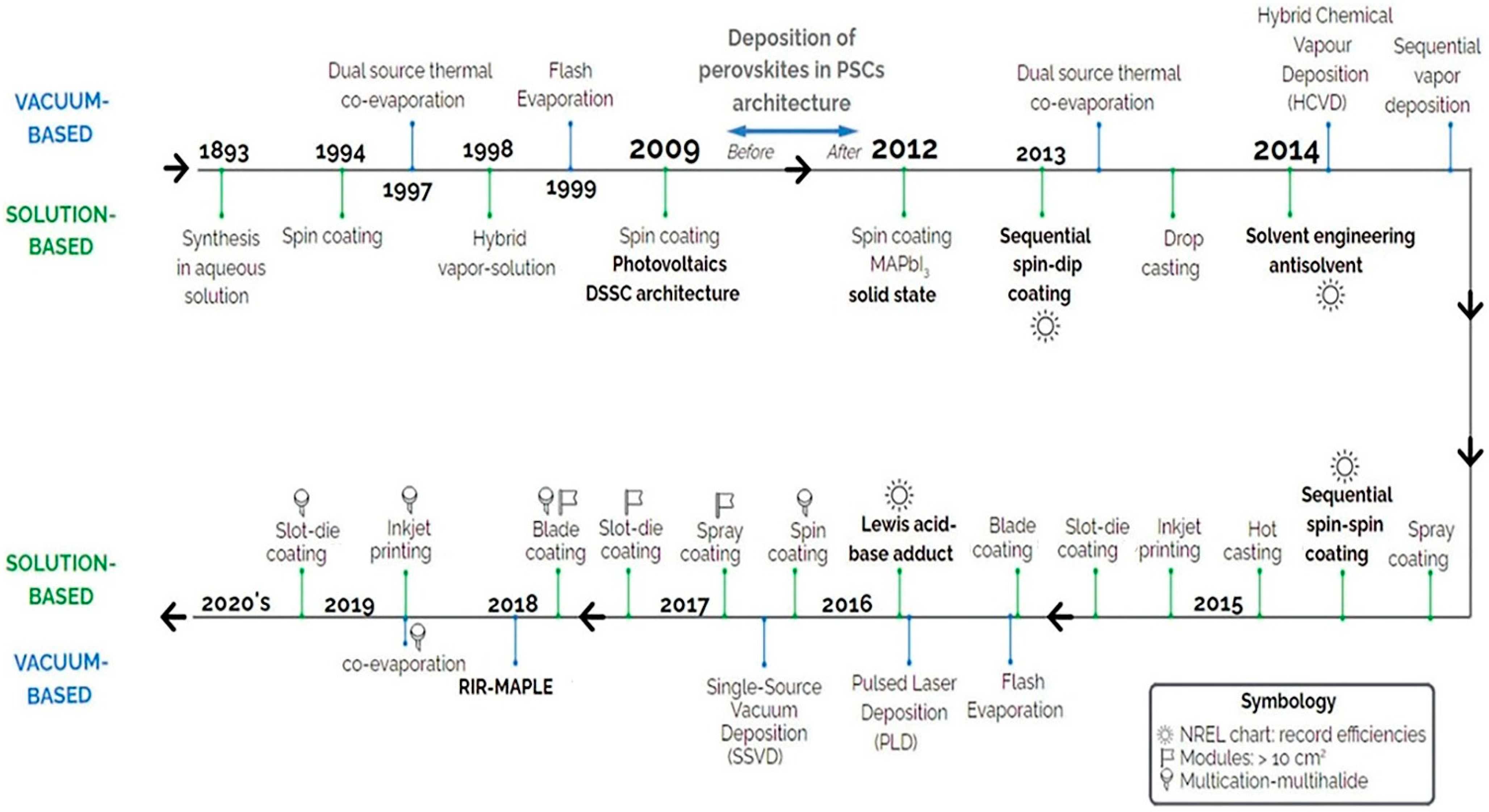
2. Large-Area PSC Preparation Methods and Fabrication Technologies

There are three critical factors for successful PSC commercialization: performance, cost, and stability. Improvements in device architecture and fabrication processes that have improved device performance have also resulted in PSC commercialization becoming an unstoppable trend. Commercialization of PSCs is now gradually being realized with the establishment of pilot production lines for perovskite photovoltaic devices possessing good performance and manufactured cost effectively using established techniques. However, device stability has continued to be an issue for researchers and industries.
Thin metal–organic perovskite films have traditionally been fabricated through solution-processed spin-coating, which permits fast iteration, optimization, and research development but is not a scalable technique for fabricating photovoltaic cells. The critical requirement for a scalable production method is low cost, which consists of capital expenditures for the necessary equipment as well as operational expenditures, including energy usage, material costs, the cost of post-treating production waste, and quality control [27,37,38]. Since the cost of contemporary PSC materials is negligible due to their ready availability, the costs of PSC manufacturing are dominated by capital expenditures and lowered by higher and faster throughputs [39]. Due to the different substrate materials, it is essential to distinguish between rigid and flexible PSCs when studying their synthesis methods. The large-area solar cell preparation methods shown in Table 1 have been successfully used to manufacture flexible and rigid PSCs [16,40,41]. Perovskite thin-film fabrication methods are divided into solution processing and vapor deposition methods [7,40]. Table 1 shows the different methods in each of these clusters. In contrast, Figure 3 shows the graphic timeline on thin-film PSC fabrication methods for inorganic and hybrid halide perovskites developed by [42] shows that for the five years, most researchers have mainly focused on solution-based then vacuum base method.
Some conclusions can be drawn from the two cluster methods in Table 1 and related works of literature:
  • In recent years, vacuum thermal evaporation has lost its position as the fabrication method of choice.
  • Spray coating and blade coating have also seen a reduction in use by PSC researchers.
  • PSC researchers have increasingly adopted ink-jet printing and slot-die coating.
  • PSC researchers are working on overcoming the technological impediments to the synthesis and commercialization of large-area PSCs.
  • Not all perovskite thin-film fabrication technologies have been used to create large-area solar cells despite some methods such as thermal evaporation having significant scalability potential.
  • In recent publications, the slot-die coating has demonstrated the highest PCE for large-area PSCs, implying that it has a high potential for ushering in PSC commercialization.
Progress in the fabrication of large-area PSCs indicates that PSC commercialization is now a reality. As a matter of fact, Saule Technologies, a start-up from Poland, launched the world’s first industrial production line of solar panels based on groundbreaking perovskite technology in May 2021. The company manufactures perovskite solar modules on thin, flexible substrates, in a variety of different colors, using a novel, room-temperature ink-jet printing procedure invented by one of the company co-founders, Olga Malinkiewicz. Malinkiewicz developed this fabrication technique in 2013 while still a Ph.D. student at the University of Valencia in Spain and this work was published in Nature Photonics in 2013 [44].

2.1. Spin Coating

Spin coating is a batch method in which a liquid film is spread by centrifugal force onto a rotating substrate [45]. The method has been extensively used to manufacture small PSCs of about 0.1 cm2 and large-area devices of 1 cm2. This method is categorized into one-step and two-step processes. Perovskite devices fabricated through spin coating have reached PCEs of over 9.4% [46].
Spin coating has potential for the production of moderately large-area PSCs if evaporation of the solvent can be closely regulated [2,40], and this has been demonstrated by the authors of [47], who prepared a large-area perovskite film of 57 cm2. The two-step sequential processing method provides better performance than the one-step method for perovskite deposition. In addition, film quality can be enhanced through controlled crystal growth and the post-annealing time [32,48].

2.1.1. One-Step Spin Coating Method

Organic halide salts (such as MAI and formamidinium iodide (FAI)) and lead halide salts (such as PbI2, PbBr2) are mixed and dissolved in a solvent such as dimethyl sulfide (DMSO) or N, N-dimethylformamide (DMF). The mixed precursor solution is coated on the conductive, electron, or hole transport layer and the absorber, followed by annealing [6,15,49,50], and the perovskite films form as shown in Figure 4a.

2.1.2. Two-Step Spin Coating Method

Halide organic and lead halide salts are dissolved in DMF and isopropanol, respectively. Next, the lead halide solution is spin-coated on the ETL/HTL, and then it is annealed. The MAI solution is then spin-coated on a lead halide surface and annealed by interdiffusion to obtain the perovskite films. Jiang et al. used a two-step spin coating method on 1 cm2 PSCs and obtained 20.1% PCE. These authors managed to control the residual PbI2 on the perovskite surface, as shown in Figure 4c [54].

2.1.3. Advantages of the Spin Coating Method

With this method, the preparation process is not complex, and the chemistry and thickness of the perovskite film can be regulated [21]. As shown in Figure 4a,b [51,52], precursor solutions that comprise polar aprotic solvents with high boiling points, for instance DMSO or DMF, can be used since the solvents can commonly be removed by centrifugal force while the substrate is spun at high revolutions per minute.

2.1.4. Disadvantages of the Spin Coating Method

With spin coating, the quality and uniformity of perovskite films decrease sharply with increasing area [21]. Issues relating to the control of stoichiometry and crystallinity have arisen due to the incomplete reaction of the precursor solution and the annealing process in the one-step solution-processing method. The spin coating method was found to be related to poor perovskite film homogeneity and to be incompatible with large-area and large-scale production [55]. The solution process and other conventional processes need lead as a precursor. However, more than half of spin coating solutions are wasted during perovskite film synthesis [56,57]. Conventional antisolvents, such as chlorobenzene, are ineffective with large-area spin coating and produce nonuniform perovskite films [23].

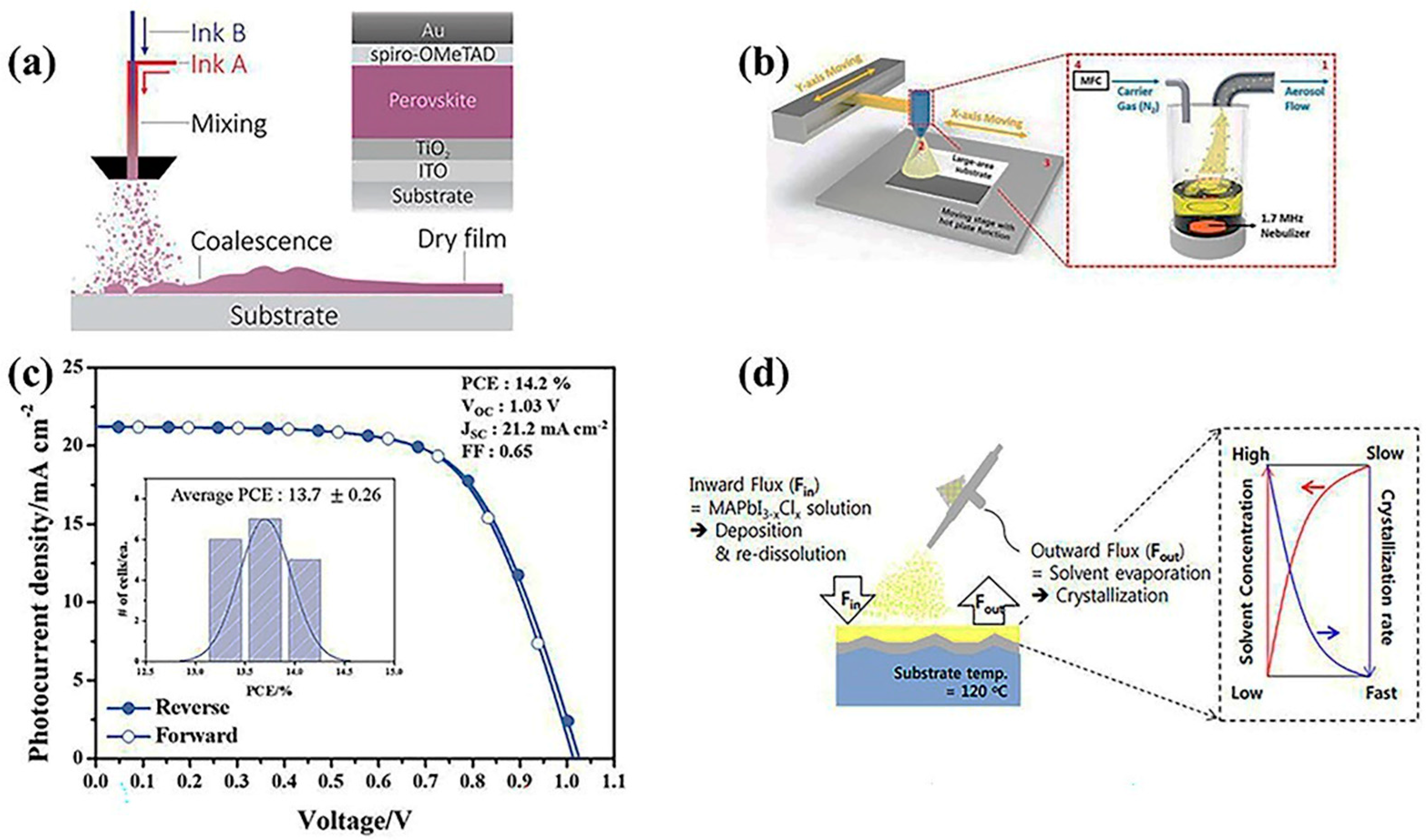
2.2. Spray Coating Methods: Spray Printing, Spray Deposition, Spray Pyrolysis, and Ultrasonic Spray

Spray coating is a low-temperature and low-ink-concentration coating method that is suitable for large-area technology and it is a widely used deposition method in the industry [16]. It is an easily scalable method for fabricating large-area thin perovskite films. Perovskite film obtained through this method displays high uniformity over large areas.
Spray coating is accomplished through a series of four distinct activities, as shown in Figure 5a: production of the ink droplets, placement of the droplets on the substrate, amalgamation of the droplets into a wet film, and film drying. Of all the scalable methods, spray coating is the most diverse. It presently encompasses two methods of deposition: one-step and two-step. One-step film deposition solutions comprise aprotic solvents [16,58,59,60]. Two-step methods use metal salts deposited by either spray coating or spin coating in an aprotic solvent lacking an acidic proton and hydroxyl and amine groups [40,61].
Spray coating is the fastest process by which a subjected fluid can be automatically driven to exhibit capillary waves and obtain a scalable substrate [21]. It is based on the atomization of a fluid and the depositing of the atomized fluid droplets onto a suitable surface. Atomization can be generated through various methods: high flow gas, ultrasonic stimulation, or cavitation of the ink itself [60,62]. The aforementioned atomization methods are generally scalable.
Figure 5. (a) Schematic of concurrently pumped ultrasonic spray coating for perovskite precursor deposition [59]. Copyright 2016 Royal Society of Chemistry. (b,c) Schematic representation of the mega-sonic spray-coating process and J–V curves of PSCs, respectively [63]. Copyright 2018 John Wiley and Sons. (d) Schematic diagram of the spray coating process [64]. Copyright 2016 The Royal Society of Chemistry.
Coatings 12 00252 g005
Ultrasonic spray coaters are the latest technology for efficiently preparing various functional thin films for photovoltaic cells [65,66]. Liquid thin-film coating technology has been developed for different applications.
Organic salts are deposited on the substrate by spray coating or immersion in an alcohol solution, using isopropanol as the solvent [67,68,69,70]. The results vary depending on the method of perovskite solution deposition employed. The single-step deposition method has been used in compositions encompassing MAI, lead iodide, and iodide chloride varieties [67,71]. The solvents used were DMF, DMSO, gamma-butyrolactone (GBL), DMF-DMSO, and GBL-DMSO; some studies used processing additives such as hydrogen iodide (HI) [71]. The highest reported PCE for perovskite films made through this method was 18% for small-area samples and 15.5% for the maximum device area of 40 cm2 [64].
Robert et al. reported the device area with the highest efficiency and good morphology without using an ultrasonic spray coater [61]. They used single-cation (MAI) mixed halide for perovskite preparation by spray coating on a preheated substrate, and this showed excellent crystallization morphology [58,60]. Ultrasonic atomization plays a crucial role in nucleation, metal polyhalide complex formation, solution optimization processes, and temperature control.
Kim et al. developed devices using the antisolvent spray coating method, which allows high-quality perovskite film to be deposited over a large area. An FTO/glass/bl-TiO2/m-TiO2/perovskite/spiro-OMeTAD/gold 16 cm2 device on the cellular level, as opposed to the module level, was created via the modified solution process in combination with a metal lattice. This cell device was found to be 12.1% efficient and overcame low PCE and poor film quality challenges associated with large-area PSCs [22].
Tait et al. used concurrently pumped ultrasonic spray coating for precise and fast optimization of the precursor ratios of PbCl2, Pb(CH3CO2)2·3H2O, PbBr2, MABr, and MAI to attain pinhole-free perovskite films with high crystallinity, and they achieved a PCE of 11.7% for 3.8 cm2 modules [16,59]. Figure 5a shows the schematic diagram of simultaneously pumped ultrasonic spray coating for perovskite precursor deposition. Perovskite layers were spray-coated with DMF inks of PbCl2:MAI and PbAc2:MAI. This technique rapidly and precisely optimizes PSCs.
Ye et al. manufactured high-efficiency large-area PSCs using NiO-based HTLs synthesized through a spray pyrolysis method. PSCs with active areas of 1 cm2 exhibited notable mean PCEs of 17.6% [72], 18.21% [73], and 19.19% [74]. A larger PSC with an active area of 5 cm2 attained a mean PCE of 15.5% [75]. The PSC based on the mesoscopic TiO2/Al2O3/NiO/carbon framework showed a PCE of up to 15.03% [76]. Using a recent facile spray deposition method for CuI film, PSCs exhibited a mean PCE of 17.6% and excellent device stability [77]. The method frequently used in large-area C-TiO2 for electron transport material fabrication is spray pyrolysis deposition [34,77,78,79,80,81,82]. Compared to the traditional spin coating method, the pyrolysis spray deposition method produces a denser TiO2 film, lessening material loss and deposition time, which results in desirable low-cost production.
Nanomaterial spray coating has been widely investigated as a means for developing semi-transparent devices due to its simple process. For example, using transparent electrodes of spray-coated silver nanowires, carbon nanotubes, and the respective composites, small 0.25 cm2 entirely solution-processed, semi-transparent PSCs with more than 10% PCEs were successfully fabricated [83,84,85,86,87].

2.2.1. Advantages of the Spray Coating Method

PSC devices can be manufactured cheaply, in large quantities, rapidly, and with low material wastage [16]. Ultrasonic spray coaters are the modern technology to be developed [66], having more uniform droplet size as well as better airflow and spray cone control. Other advantages of the spray coating method compared to the conventional antisolvent dropping method include less antisolvent usage, rapid distribution of the antisolvent, faster supersaturation, even nucleation, and better uniformity over a large area.

2.2.2. Disadvantages of the Spray Coating Method

Overall, the PV performance of PSCs synthesized by spray coating is poorer than that of PSCs synthesized by blade or slot-die coating. Thus, the spray coating method needs to be optimized for large-area perovskite film fabrication [23].
The deposited perovskite film morphology appears to be low across all single-step research, with nonuniform crystallization, mostly dendritic, and the absence of full coverage of the underlying transport layer [40]. This results in PV cell devices having lower open-circuit voltages, short-circuit currents, and fill factors compared to their spin-coated counterparts, possibly emanating from low shunt resistance [58,60]. Other undesirable traits of this method include surface defects, overspray, and challenges with controlling the film thickness [88].

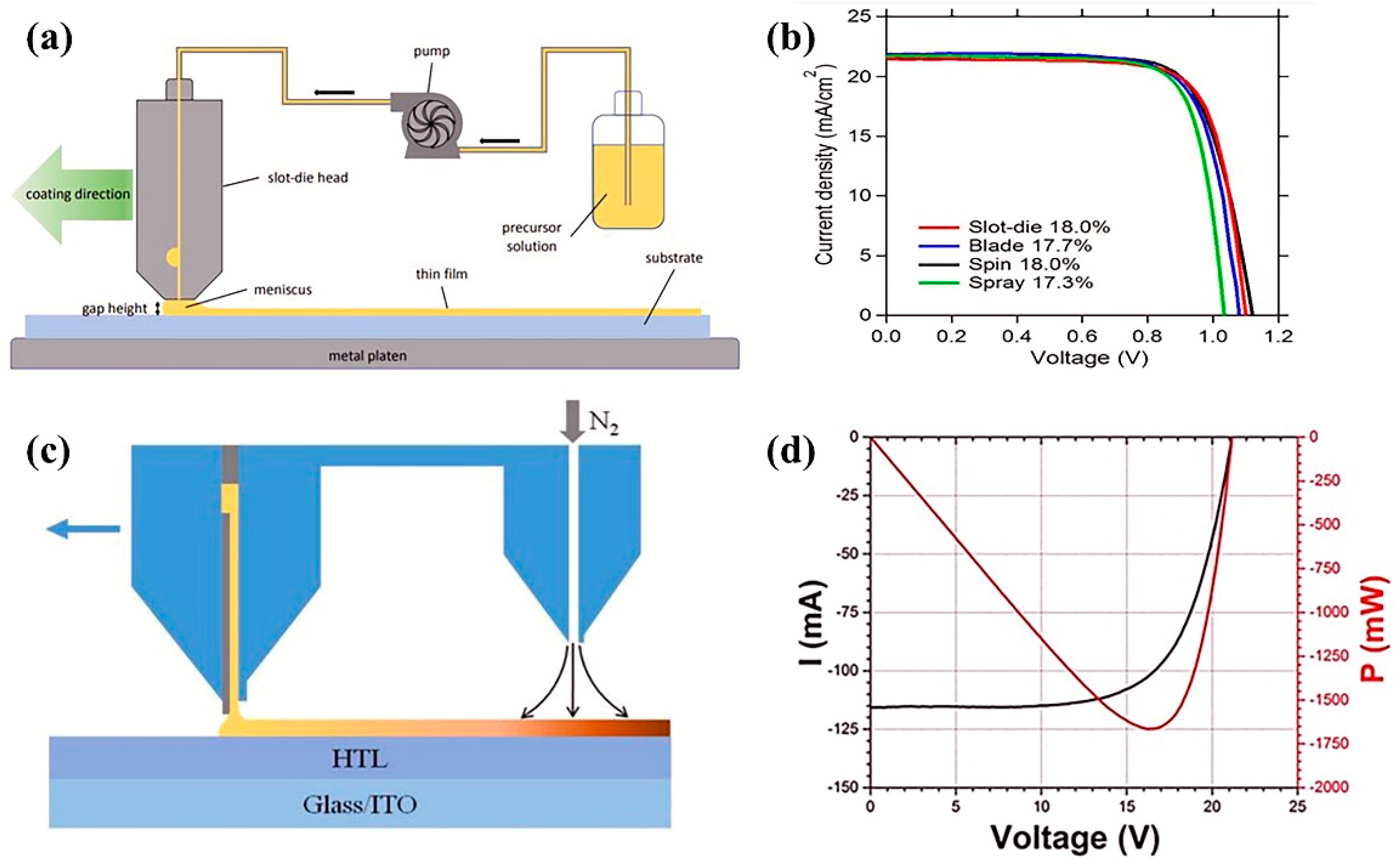
2.3. Slot-Die Coating Method

Slot-die coating is a process in which ink is metered through a microfluidic metal die machine. The die is machine structured with a thin channel to spread ink over a moving substrate surface [45]. A graphic depiction of the process is shown in Figure 6.
The surface is typically a bendable substrate such as plastic. The head is generally positioned horizontally on a roller to negate the effects of gravity on the fluid in the head and to control wet film formation during high-speed coating (Figure 6, right). The head is positioned vertically over a glass substrate or flattened surface (Figure 6, left). The wet film formation depends on geometry, web speeds, and the fluid feeding rate. Therefore, coating processes depend on the wet film’s thickness, chemistry, and stable microfluidic boundary conditions that are affected by its geometry [89]. Slot-die coating has traditionally been a popular method in the organic PV community based on its non-viscosity and low boiling point resulting from fully enclosed environmental deposition. The composition fluctuations due to solvent evaporation loss can be mitigated. Sheet-to-sheet slot-die coating is a non-contact film synthesis method based on pumping a precursor solution over a die with a definite split, as illustrated in Figure 7a. Slot-die coating makes use of an uninterrupted supply ink reservoir with a thin slit to smear ink over the substrate, and the film thickness can be controlled [90,91].
Zhao and Zhu fabricated four different PSC devices with four different deposition methods: spin coating, blade coating, spray coating, and slot-die coating [91]. Figure 7b shows that all other conditions were kept constant [92]. The slot-die-coated active layer achieved the highest average PCE and an 18% reverse J–V sweep, as shown in Figure 7b. Gao et al. used this method compatible with potentially large-scale, roll-to-roll commercial processes, as illustrated in Figure 7c, and achieved an average PCE of 15.57% [92]. Galagan and co-workers fabricated large-area PSCs of 168.75 cm2 and 149.5 cm2 by slot-die coating and obtained average PCEs of 11.1% and 11.8%, respectively, as shown in Figure 7d [93].

2.3.1. Advantages of the Slot-Die Coating Method

Solvent evaporation loss can be improved by using high-precision materials film, accelerating PSCs’ industrial-scale production, and enhancing their potential commercial value. PSC devices with good replication efficiency could be processed completely via slot-die coating in ambient conditions [94]. Slot-die coating deposition methods are rapid and carried out in large, well-controlled areas with little solution waste, and they are compatible with continuous roll-to-roll technology. Therefore, slot-die coating is an excellent method of choice for fabricating large-area perovskite thin films [95,96,97].

2.3.2. Disadvantages of the Slot-Die Coating Method

The deposition of precursor solutions on a hot substrate at 90 °C causes the instant formation of large black crystal-like perovskite films. Slot-die-coated perovskite has been reported to have high roughness in the resulting films [32,98]. Loss of MAI was observed at substrate temperatures higher than 110 °C, and PSC devices prepared at such high temperatures had lower PCEs [94,95]. The risk of partial delamination of the perovskite film from the TiO2-blocking layer is higher than with spin-coated films [94,97]. Therefore, this method is less appropriate for modifying the active area [2,32,97].

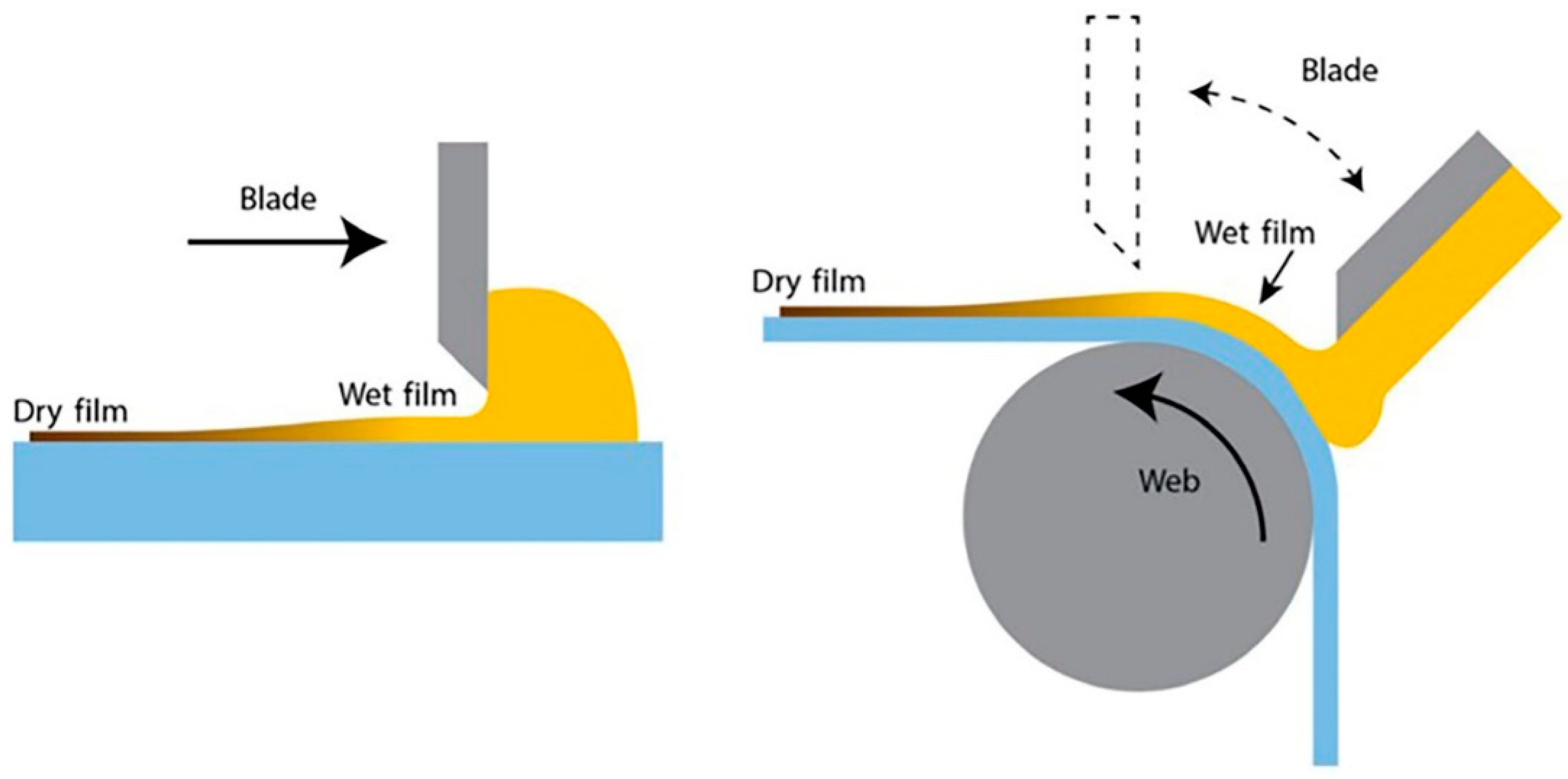
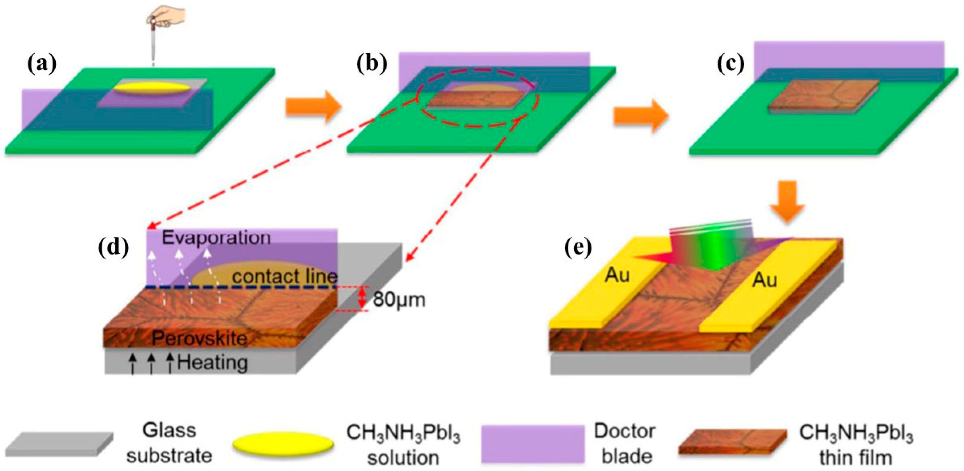
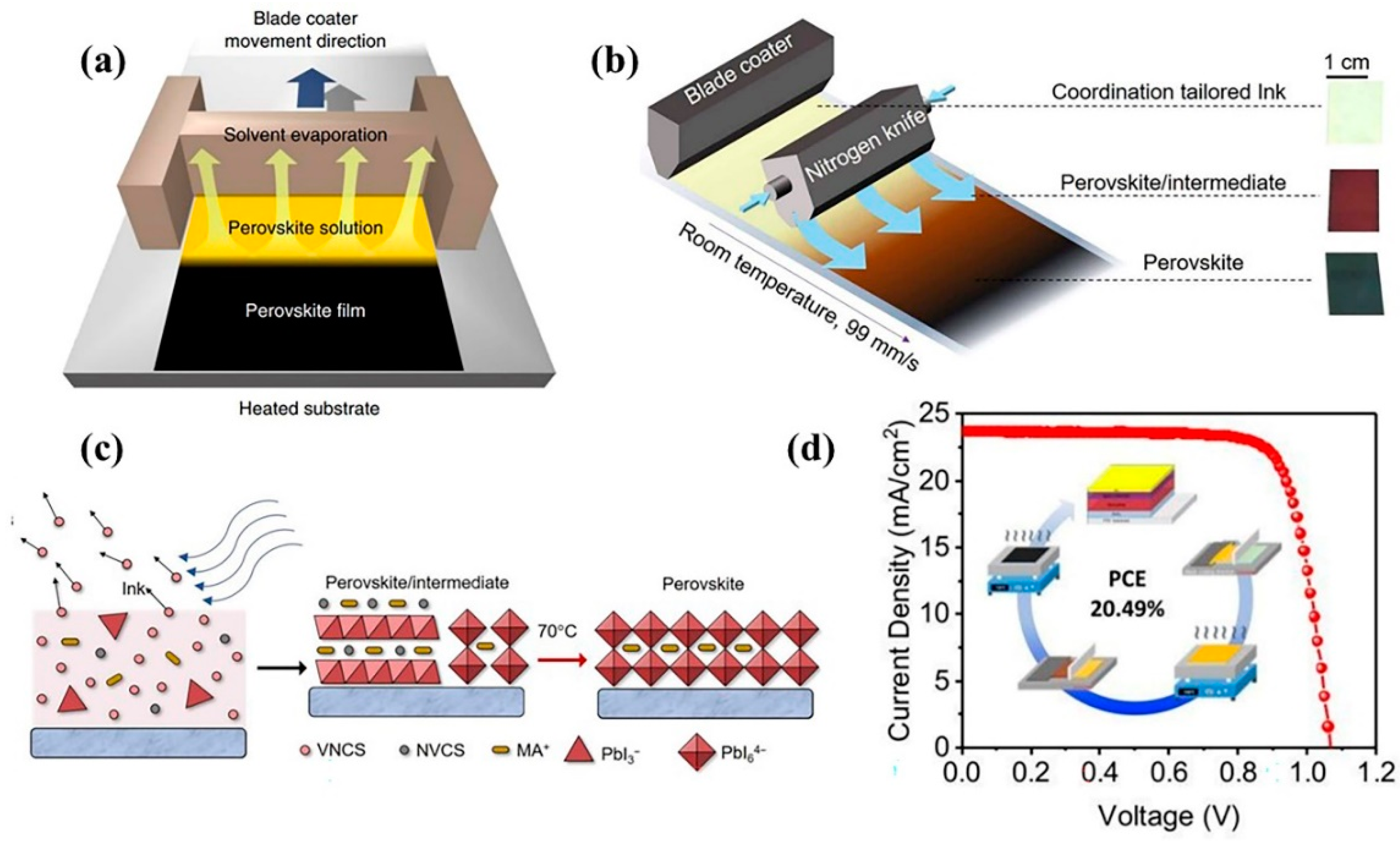
2.4. Blade-Coating Method

Blade coating is a method in which a blade moves across a surface or vice-versa in the case of roll-to-roll coating [45,99]; it is also known as doctor-blading and knife-over-edge coating. The blade spreads pre-dispensed ink and forms it into a thin liquid film, as shown in the schematic diagram Figure 8. The film is then dried, creating a solid thin film. This is the most used synthesis technique for fabricating large-area perovskite films. It has been used in several PSC studies to synthesize high-performance cells with areas of over 10 cm2. Various studies have demonstrated that the perovskite film quality can be enhanced by controlling the processing temperature [100,101]. Recently, additives have been utilized to realize dense perovskite films with smaller pinholes and homogeneous crystal morphology [102,103]. Blade coating has been commonly used as a single-step deposition method for perovskite films [33,34,99,104,105,106,107,108] and recently for producing perovskite PVs with a 20% [104,105,109] scalable solution method.
Razza et al. used this method to fabricate a PSC module with an active area of 10.1 cm2 and recorded an average PCE of 10.4% [34], while previously, these authors reported a PCE of 4.3% for a cell area of 100 cm2 [34]. Gao et al. reported a method for fabricating ultra-long nanowire arrays and highly oriented CH3-NH3PbI3 thin films in ambient environments. This method integrated large-scale roll-to-roll micro gravure printing and doctor blading to fabricate perovskite nanowires of 15 mm in length [110].
Figure 8. Schematic diagram of the in-situ doctor blading method for fabricating CH3NH3PbI3 films. (a) CH3NH3PbI3 solution dropped before the doctor blade is brought close to the substrate. (b) CH3NH3PbI3 crystal nucleate and growth during doctor blading. (c) The magnified schematic in (b). (d) CH3NH3PbI3 crystal film is growing with the movement of the doctor blade, and large-area CH3NH3PbI3 film was formed on the substrate. (e) Schematic of CH3NH3PbI3 photodetector synthesized through doctor blading [111]. Copyright 2017 Elsevier.
Coatings 12 00252 g008
Preheating the substrates is known to accelerate the blade coating process and prevent the development of acicular crystals in the perovskite films, as shown in Figure 9a [99]. Huang et al. sped up liquid-layer drying at room temperature by introducing a nitrogen knife (N2 knife) after a fixed distance and applying a nitrogen flow, as shown in Figure 9b. This innovation produced a certified PSC module of 63.7 cm2 effective area and with a mean PCE of 16.4% [112]. Figure 9d shows a J–V curve of the high-performing PbI2-TBP-PS device that obtained average efficiencies of 20.49% [113] and was fabricated through a two-step sequential blade-coating method.

2.4.1. Advantages of the Blade-Coating Method

This process offers close control of the separation between the blade and the substrate as well as the treatment temperature. It is a relatively simple method compared to the other single-direction coating methods. It is the cheapest small-scale PSC preparation method with the most adjustable and cost-effective film deposition tunable to specific applications [40,114]. Blade-coated perovskite films are indeed polycrystalline, homogeneous, and pinhole-free, and they show long-lived photoluminescence [115,116].

2.4.2. Disadvantages of the Blade-Coating Method

This method reportedly has a problem of significant inconsistency in blade coating quality. In its simplest form, blade coating does not use a fully enclosed ink reservoir, as is the case with the other solution processing methods. As ink chemistry may change over time [40], control of solution chemistries is required to improve the grain growth, nucleation temperature, and crystallization temperature [34,115,116,117].

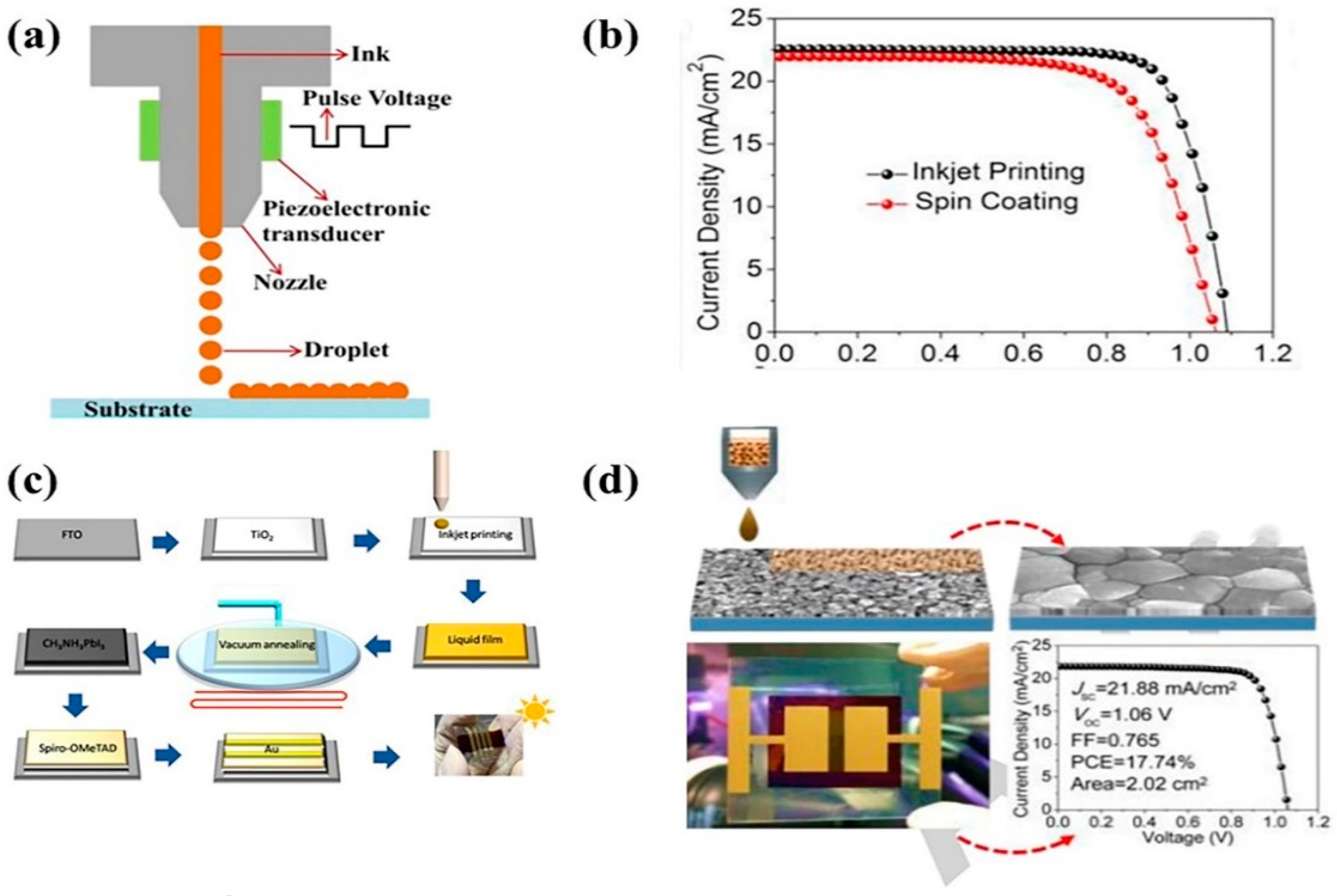
2.5. Ink-Jet Printing Method

This is a non-contact printing method with direct control of ink deposition, which greatly reduces material utilization and waste. Quintilla et al. reported the fabrication and optimization of multipass inkjet-printed PSCs [118]. The perovskite film’s thickness and grain size were carefully controlled during multipass ink-jet printing with MAPbI3 ink, producing PSCs with a high average PCE of 11.3% [118].
Ink-jet printing is a method through which a microfluidic cavity is subjected to pressure change, thereby causing the solution to jet out of a microfluidic nozzle. This pressure change can be created through various methods, including thermal and structural sources acting on the microfluidic nozzle. Most ink-jet printing methods demonstrate piezoelectricity of the ink-jet printhead based on a micro-electro-mechanical system, which provides controllable microfluidic jetting through a silicon-etched nozzle. Ink-jet printing, such as ink-jet printers, uses numerous jetting nozzles in a single mobile print head to control the planar thin film thickness and improve the reliability and speed, as shown in the schematic diagram in Figure 10a [119]. For comparison purposes, Figure 10b shows the J–V characteristics of inkjet-printed and spin-coating-based PSCs [119].
Images of PSCs with a PCE of 13.27% at 4.0 cm2 effective area that was based on printed CH3NH3PbI3 are shown in Figure 10c [120]. Other researchers who fabricated large-area PSCs through ink-jet printing innovations include Song et al., who employed a two-step printing technique to chemically engineer a lead-iodide precursor ink before reacting this ink with MAI vapor, producing MAPbI3. The resultant PSC device, which measured 2.02 cm2 in area, yielded a PCE of 17.74% (Figure 10d) [121].
Figure 10. (a) Schematic diagrams for continuous ink-jet printing methods. Copyright 2018 Royal Society of Chemistry [119]. (b) J–V characteristics of ink-jet printing and spin coating-based PSCs [121]. Copyright 2018 Elsevier. (c) Schematic diagram of PSC fabrication through ink-jet printing with vacuum annealing [120]. Copyright 2018 John Wiley and Sons. (d) J–V curves of PSCs on ink-jet printing with active area 2.02 cm2 [121]. Copyright 2018 Elsevier.
Coatings 12 00252 g010

2.5.1. Advantages of the Inkjet-Printing Coating Method

This method permits direct modelling of the printed layers, removing the necessity for laser etching of photoactive films as required in a PV module fabrication. Generally, single-step deposition produces poor deposit morphology, possibly due to the overlap of droplets, which can alter nucleation and chemical concentration due to dissolving and recrystallizing films [120,122,123]. However, similarly to spray coating, two-step ink-jet processes produce better deposit morphology and larger grains [121,124].
Ink-jet printing enables modified intricate cell shapes for particular functions, such as wearable or small utility power sources and building-integrated photovoltaics [125]. Saule Technologies use this method to manufacture 1 m wide perovskite BIPVs and electric vehicle charging ports at a commercial scale. Thus, it is a very scalable technique for fabricating PSCs. A significant advantage of continuous and other ink-jet printing systems is the absence of a need for physical contact or critical spacing between the jet and the substrate, making it appropriate for printing on uneven, curved, or pressure-sensitive surfaces. Further, the method can use any adequately fluid and conductive material or solute that is soluble in a conducting fluid. While all methods allow 2D freedom of design, ink-jet printing offers faster turnover, and a system can be created or changed without delay [126].

2.5.2. Disadvantages of the Inkjet-Printing Coating Method

For titania-based PSCs, ink-jet printing of the compact TiO2 films is difficult because of the hydrolysis of sol–gel precursor ink at room temperature, which leads to nozzle blockage. Depositing a thin, defect-free, consistent, and unbroken film on the rough FTO substrate surface is challenging, and the film reportedly destabilizes and becomes inhomogeneous upon drying. The c-TiO2 layer mostly affects the device’s fill factor [125] because ink crystallizes quickly during printing, and the printed perovskite film becomes discontinuous, with increasing defects. This strictly limits the application of ink-jet printing technology to the fabrication of perovskite photovoltaic devices [127]. The major disadvantage of the ink-jet process is the unavoidable waste of ink-jet material during deposition. Even though undesirable droplets of printing material can be collected in a drain and recycled to become part of the printing ink, this used ink may become contaminated [126].

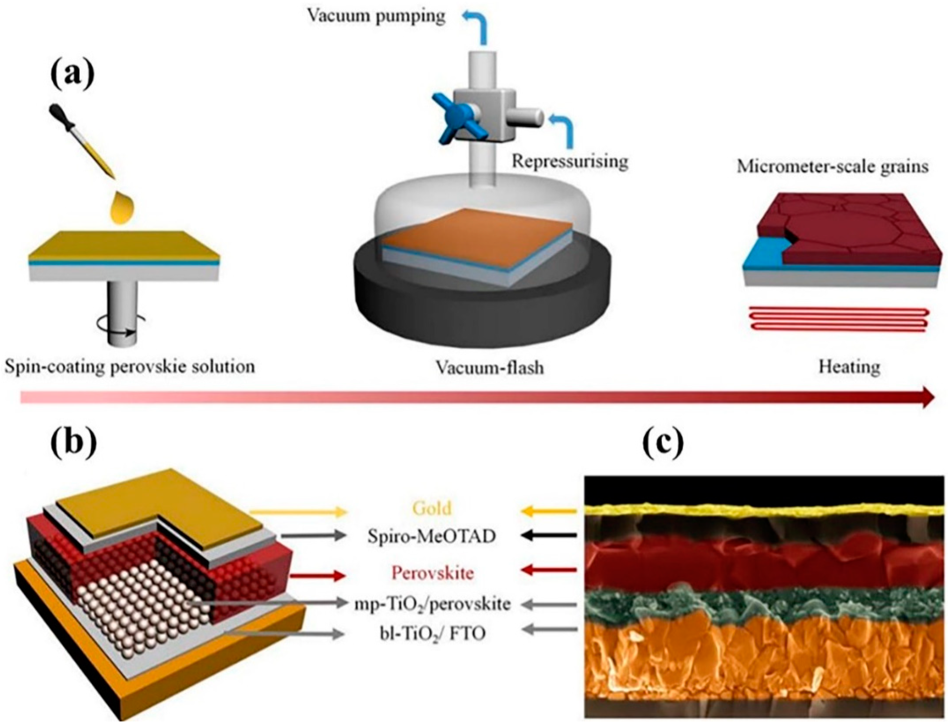
2.6. Vacuum Flash-Assisted Solution Method

The vacuum flash-assisted solution (VAS) method allows fast and well-controlled removal of the solvent. In so doing, it promotes rapid crystallization of the perovskite precursor phase [128]. Figure 11a shows the necessary steps of perovskite film fabrication using the VAS method. The perovskite precursor solution composition, FA0.81MA0.15PbI2.51Br0.45 comprising DMSO with a nominal Pb to DMSO ratio of 1:1, was initially spin-coated on top of a mesoporous TiO2 film [129].
Grätzel et al. used a VAS method to manufacture high-efficiency large-area PSCs [17]. Figure 11a illustrates the nucleation and procedures during perovskite film formation via vacuum flash-assisted solution processing (VASP). The authors fabricated perovskite films with larger crystal sizes than those fabricated using standard solution processing techniques (Figure 11b), and the resultant PSCs attained a peak PCE of 20.5% for an area of 1 cm2 [17].

2.6.1. Advantages of the Vacuum Flash-Assisted Solution Method

Upon thermal annealing, the precursor phase produces highly oriented, crystalline perovskite films of excellent electronic quality that can be grown on various substrates. The VAS method is readily scalable to the industrial level and eliminates hysteresis in the J–V curves [130,131]. Li et al. found the VAS method versatile concerning precursor components and perovskite composition variations [17]. The perovskite thin films deposited through vacuum methods offer the advantages of the sublimed materials’ intrinsic purity, controlled film thickness, and low substrate-fabrication temperature. The latter is essential for the compatibility of perovskite technology with plastic electronics and the fabrication of lightweight, flexible devices using traditional inorganic solar cells in the form of tandem devices. Additionally, a significant benefit lies in avoiding the toxic solvents employed for perovskite solution processing [132].

2.6.2. Disadvantages of the Vacuum Flash-Assisted Solution Method

The resultant perovskite films are amorphous or have poor crystalline structures, which causes low charge-carrier transport [133]. Despite the good PCEs, large-area PSCs made through this process suffer from poor stability [57].

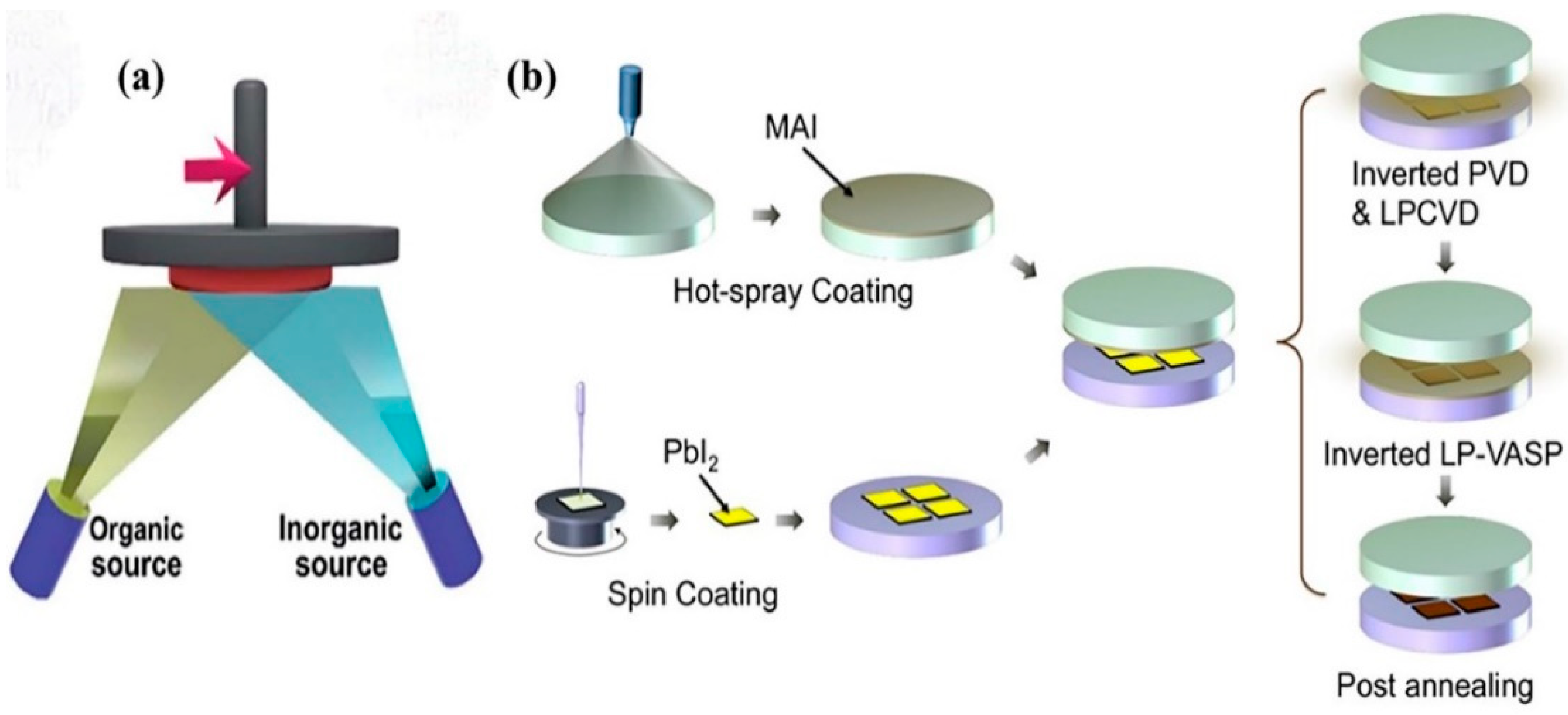
2.7. Chemical Vapor Deposition Method

Chemical vapor deposition (CVD) is an established, low-cost, and highly efficient technology for fabricating various semiconductor materials from gases. Compared to the PSC device fabrication process using the spin coating method, CVD methods produce significantly higher device performance, as shown in Figure 12a. The CVD variants include dual-source evaporation [134], vapor–solid reaction [135], and the vapor-assisted method, [14]. Liu et al. fabricated high-quality and uniform perovskite films using the dual-source co-evaporation method [134]. This method is reliant on high temperatures and high vacuum conditions. Alternatively, the vapor–solid reaction method can be used as a substitute, which deposits the perovskite film at a low temperature (Figure 12b) [135]. Chen et al. used this method on a 64 cm2 PSC device and obtained a mean PCE of 6.0% over an active area of 1.5 cm2 [135].

2.7.1. Advantages of the Chemical Vapor Deposition Method

This particular method produces films of uniform thickness over a large area. It has the potential to be used commercially for growing films with more complex perovskite compositions for high-performance PSCs [40]. Vapor-based methods are well known and used widely in the coating and semiconductor industry [132,136]. Multizone CVD provides accurate control of the pressure, gas flow rate, MAI temperature, and substrate, enhancing the process’s reproducibility [137]. Interestingly, the CVD method uses air at atmospheric pressure as the carrier gas, which is advantageous for commercial production [136,138] due to it optimizing the crystallization kinetics, mostly through in situ annealing under an organic vapor atmosphere [132].

2.7.2. Disadvantages of the Chemical Vapor Deposition Method

The perovskite films prepared through this method are amorphous with a flawed crystalline nature, which causes low charge-carrier transport [139], similarly to those produced by the vacuum flash-assisted solution method. Vapor deposition processes require specific vacuum pressures, increasing operating costs [57].

2.8. Sequential Evaporation Method

This method involves the separate vapor deposition of multiple film layers on top of each other and the subsequent conversion of these multiple film layers through diffusion and recrystallization. First, the metal halide layer is deposited on top of the conductive glass and then on the organic halides, as shown in the SEM images in Figure 13. The sequential deposition demonstration of MAPbI perovskite films showed a significantly lower small-scale PCE of 5.4% for a device without a hole-transporting layer [140]. However, this method might not be ideal for optimum commercial scaling as the throughput and alternating evaporation might slow material utilization. The highest efficiency achieved for sequentially evaporated PSCs was 17.6% for small-area devices; this was accomplished by optimizing the system’s pressures through the evaporation steps, which also had a binding effect on the morphology [141].
Figure 13 shows SEM images of perovskite films fabricated through a 240 nm metal halide reaction. In the solution-processed two-step method, a final perovskite film thickness of 480 nm was observed in the medium and high organic halide pressure samples [142].

2.8.1. Advantages of the Sequential Evaporation Method

Chen et al. observed that when optimized, this method could lead to well-performing PSCs of 15.4% efficiency for small-area devices [15,132]. Compared to solution processes, vacuum evaporation produces homogeneous and dense films with high replicability and close thickness control. It permits the manufacture of multilayer films without chemical alteration of the primary layers, allowing the synthesis of heterojunction devices with high performances [143]. Furthermore, this method is useful for fabricating a tandem cell structure as it averts solvent damage to the layers beneath the perovskite film [23].

2.8.2. Disadvantages of the Sequential Evaporation Method

This method might prove difficult for commercial scaling as the throughput and material of the alternating evaporation might slow utilization. Vacuum application results in high costs, as is also the case with the other vapor-based methods [57].

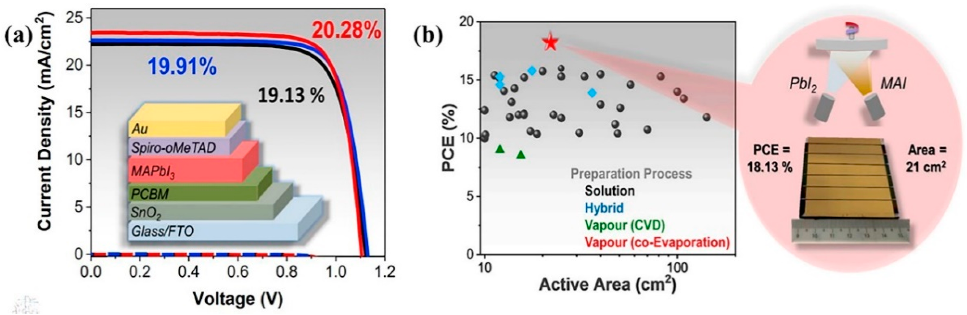
2.9. Co-Evaporation Method

This method is the most applicable vacuum-based process for several applications. The perovskite films are prepared inside a high-vacuum chamber with a pressure of 10−5–10−6 mbar, where the precursor solutions are loaded in separate crucibles and heated to their corresponding sublimation temperatures [132]. Co-vapor-deposited PSC films are smooth and homogeneous, with modules achieving high PCEs of 16.5% [130]. Additionally, the method enables the preparation of multilayer films and is completely compatible with conventional semiconductor manufacturing methods.
Li et al. positively demonstrated the scalability of thermally co-evaporated MAPbI3 layers in PSCs. As shown in Figure 14a, MAPbI3 film deposited, by means of the thermal co-evaporation process, as the absorbing layer achieved a PCE of 20.28% with a 0.16 cm2 active area, and had minimodules of 21 cm2 active area, attaining (at that time) record PCEs of 19.13% [144], as shown in Figure 14b.

2.9.1. Advantages of the Co-Evaporation Method

Perovskite crystallite grain size appears significantly smaller with this method, which leads to smoother films. Co-evaporation takes advantage of sublimated compounds’ intrinsic purity and enables close control of perovskite film chemistry and thickness [130]. The perovskite film can be completely synthesized without any thermal treatment if inorganic–organic precursors are stoichiometrically balanced, which is essential for temperature-sensitive substrates such as plastic foils. Elimination of the annealing step enables the deposition of perovskite solution on any molecular transport material [132]. Perovskite films prepared through this process are more homogeneous, with greater adherence to substrates than those prepared through spin-coating. They are denser and more porosity-free and, thus, more compatible with planar solar cells [55].

2.9.2. Disadvantages of the Co-Evaporation Method

The main challenge is controlling the vaporization rate of MAI, which is due to the high vapor pressure. The process is comparatively slow and requires accurate periodical calibrations to properly maintain the deposition rate and precursor ratio [130]. As mentioned earlier, vacuum technology tends to be costly; this makes the process expensive [57]. The relatively high vapor pressure of organic cation precursors such as MAI causes the compound to condense incompletely outside the evaporation cone region [132]. Vapor-based methods for commercial perovskite optoelectronics production are not yet common because of the sophisticated infrastructures required. The process also uses a variety of vapors, making control of the precursor stoichiometry challenging [143].

2.10. Flash Evaporation Method

In this process, the perovskite materials are positioned on a metallic heater and transferred to a vacuum. A large high-current voltage is transmitted through the metal heater, which activates all the perovskite substance, causing it to swiftly vaporize and condense onto a substrate to form a thin perovskite film. Longo et al. established that the flash evaporation method could be applied for the deposition perovskite materials, as shown in Figure 15a–c [130]. The device’s external quantum efficiency (EQE) and the perovskite layer’s UV–visible light absorption spectrum are shown in Figure 15d.
Two-dimensional (2D) and three-dimensional (3D) layered metal halide perovskites doped with aliphatic or aromatic ammonium cations have been synthesized through this method. The hybrid film is synthesized at temperatures that are sufficiently high for the inorganic material to volatilize without deteriorating the organic part [40,130,145]. Homogeneous and smooth polycrystalline MAPbI3 thin films of the required thickness can be achieved by carefully adjusting the process variables. The final layer’s thickness and homogeneity are attained if the metal heater is coated with the deposited material. Longo et al. obtained a PCE of 12.2% for a PSC fabricated through this technique, as shown in Figure 15e [130].

2.10.1. Advantages of the Flash Evaporation Method

The final film thickness is controlled by the thickness of the bulk precursor film. Perovskite films show a high degree of homogeneity and minimal surface roughness, which are essential for PSC implementation in optoelectronic devices [130]. The method is suitable for the deposition of powder precursor hybrid perovskite layers. This deposition process is scalable, additive, and quite fast, making it appealing for the industrial scale manufacture of PSCs [130]. Lead halide layers can be altered to become highly crystalline perovskite films within minutes at low-vacuum conditions with a pressure range of 1–10 mbar. Solar cells that used these perovskite absorbers showed PCEs exceeding 16% [132]. Flash evaporation technologies permit the preparation of composite structures of different organic–inorganic materials suitable for the production of tandem solar cells.

2.10.2. Disadvantage of the Flash Evaporation Method

As with all vapor-based methods, this one requires a specific vacuum level, resulting in high costs [57].

2.11. Vacuum Thermal Evaporation Method

With this method, materials are sublimated by heating them under high vacuum conditions (pressures ≤ 10−6 Pa) and allowing the resulting vapor to condense onto a cooler substrate [40]. The evaporated particles are extended under high vacuum conditions. The sublimated particles move away from the heated source in a deposition cone to reach the substrate. The film’s deposition uniformity depends on the distance from the evaporation source to the substrate. The reduced material production resulting from parasitic condensation on the vacuum chamber walls is a trade-off [40]. Large-scale manufacturing processes use linear deposition sources with a substrate that moves orthogonally through the elongated evaporation cone.
Cimaroli et al. used the vacuum thermal evaporation method to produce perovskite films for the comparison of low-temperature processed SnO2 at 185 °C with high-temperature processed SnO2 at 500 °C [146]. The device architecture (FTO/SnO2/MAPbI3/Spiro-OMeTAD/Au) is shown in Figure 16a; the authors achieved a PCE of 15.28%. Figure 16b shows the schematic diagram of the deposition setup. Metal halide and MAI were used as evaporation source materials [147].
Figure 16c shows the hybrid deposition method’s schematic and the transparency spectra of the perovskite film deposited through the hybrid deposition method. Wang et al. used this method to fabricate a semi-transparent PSC and obtained 8.6% PCE [147]. Borchert et al. fabricated large-scale FAPbI3 film (8 × 8 cm2), as presented in Figure 16c, and achieved a PCE of 15.8% [43], as shown in Figure 16d. This PV device achieved high charge-carrier mobility, μ, of 26 cm2 V−1 s−1 as indicated in Figure 16c, exceptional optical properties, and bimolecular recombination constant of 7 × 10⁻¹¹ cm3 s−1.

2.11.1. Advantages of the Vacuum Thermal Evaporation Method

This is the simplest and most widely employed vacuum deposition method. The thermal evaporation method is scalable and suitable for the industrial fabrication of PSCs. No solvent is used in this fabrication method. The materials can be consistently coated on substrates, especially ultrathin layers. The film thickness can be tightly controlled by monitoring the deposition rates of each precursor substance. The thermal evaporation method is well-suited for the characterization methods available under ultrahigh vacuum [43,148].

2.11.2. Disadvantages of the Vacuum Thermal Evaporation Method

If outsized vacuum chambers are used, the comparatively long distance between the source and the substrate diminishes the deposition rate and increases material wastage. The material deposition rate also fluctuates, which is a significant disadvantage. Vacuum technology is quite costly, lowering the attractiveness of this method [149]. Currently, the PCEs of PSCs synthesized through concurrent multisource deposition lag behind those of their solution-processed counterparts, and solution processing tends to have a much lower equipment entry barrier.
The poor stability of PSCs is a well-documented impediment to the commercialization of this method. Many important methods for improving PSC stability depend on additives, but these are difficult to implement during vacuum thermal evaporation. Additionally, there are multiple challenges that are peculiar to vapor deposition; for example, optimizing source evaporation rates and growth processes and negative interactions between volatile substances. Vacuum thermal evaporated PSCs tend to have exceedingly small grains, which negatively affects the device stability. Exposure to vacuum causes the degradation of both 3D and 2D perovskites. Any remaining solvent in the final perovskite film can negatively affect solar cell device performance [148].

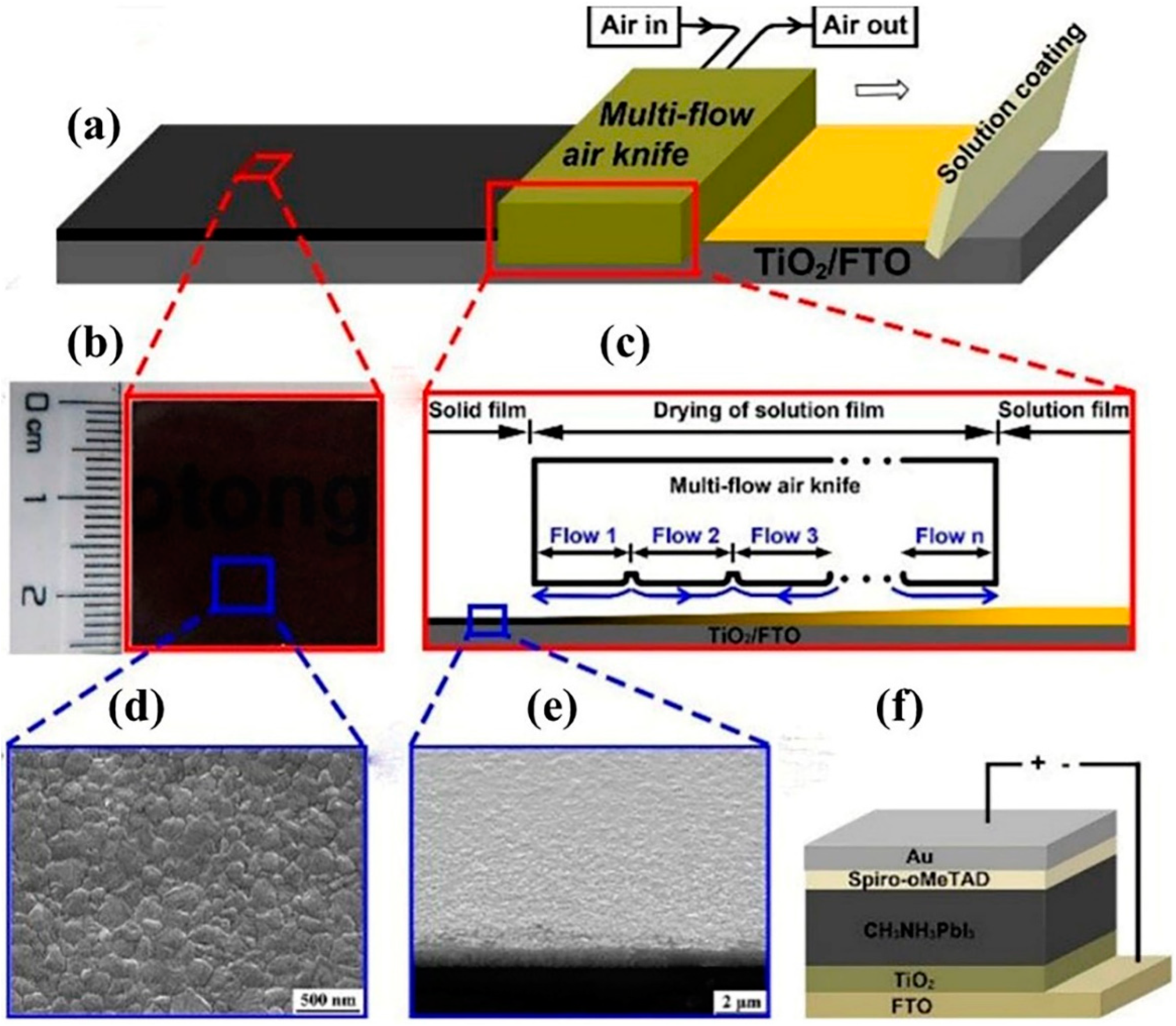
2.12. Multi-Flow Air Knife Method

Gao et al. fabricated highly efficient PSCs composed of a perovskite film dried using the innovative multi-flow air knife (MAK) method in ambient conditions, as illustrated in Figure 17. Through this method, these authors produced large-grain, homogeneous, and pinhole-free perovskite films of 4.98 nm thickness. The same authors subsequently achieved a PCE of 11.70% for large-area PSCs with an active area of 1 cm2 and obtained a high PCE of 17.71% with an active area of 0.1 cm2 [150], suggesting that the MAK method is promising. However, this high PCE was achieved by optimizing the airflow rate to 300 L min−1 and the distance between the air knife and the substrate surface to 1 mm.

2.12.1. Advantages of Multi-Flow Air Knife Method

The MAK method is very effective for drying solution films without limitations in terms of solvent types and film dimensions. It can, therefore, be readily adapted to large-area PSCs. Devices also show excellent replicability with high-quality films. Thus, this method promotes low-cost mass production, highly efficient PSCs, and high-quality perovskite films [150].

2.12.2. Disadvantages of Multi-Flow Air Knife Method

According to Gao et al., air-assisted flow is unsuitable for drying large-area solution films in ambient air since it results in inhomogeneous morphologies and blurry, wavy crystalline structures. The authors concluded that the space between the MAK and the solution film should be carefully controlled. If it is greater than 1 mm, the perovskite films develop significant pinhole porosity with otherwise crystalline grains morphing from uniform, compact, and isometric to large dendritic crystals [150]. This anomaly worsens with increasing separation between the MAK and the liquid surface. The airflow rate must also be optimized to the liquid surface distance for a defect-free perovskite film. This requires a finely tuned process control system, which adds to the capital cost of the equipment.
Table 2 encapsulates the successful large-area PSC application of the thin film fabrication methods discussed in this paper, as reported in published articles. Insights from the table are as follows:
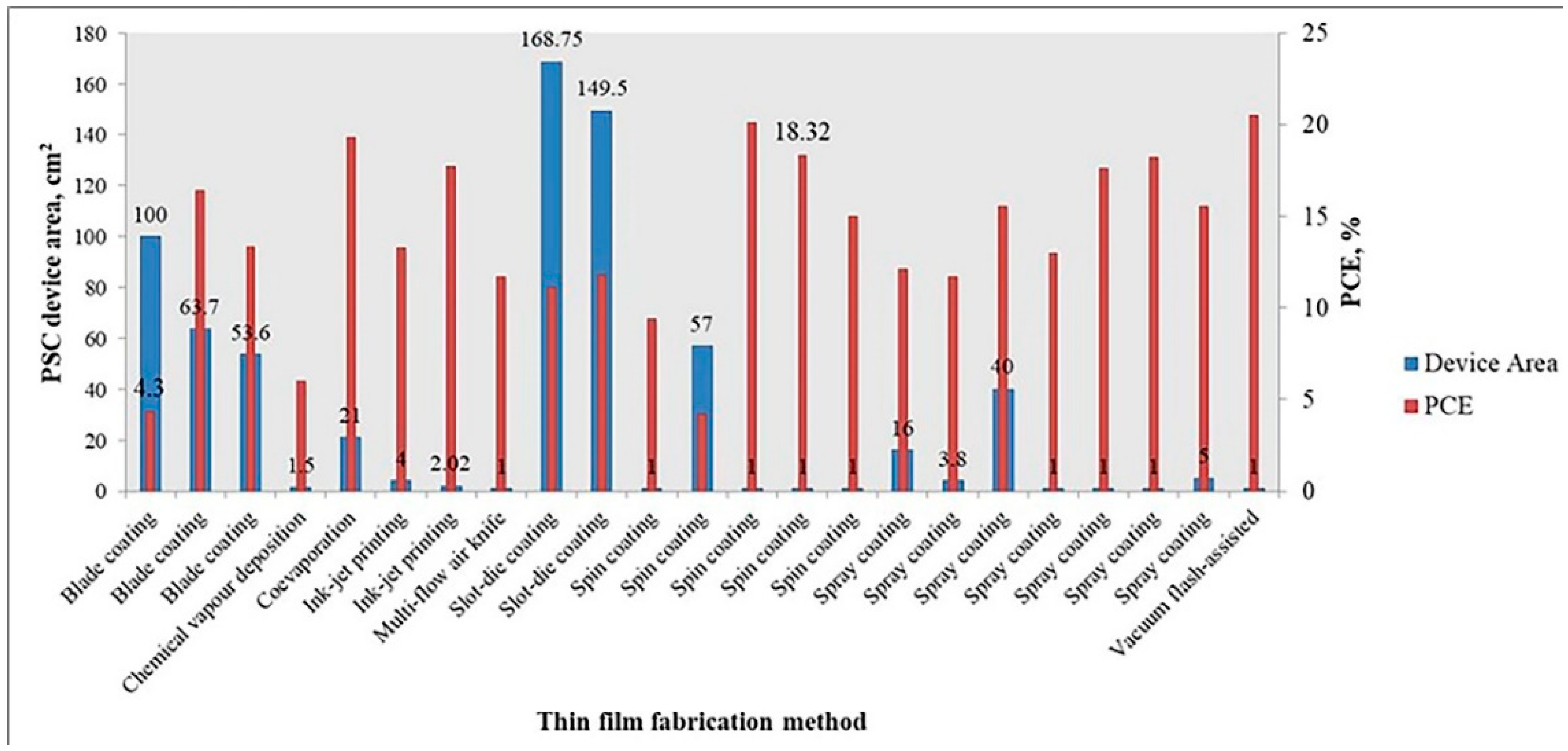
  • In terms of the sizes of fabricated large-area PSCs, the ranking in descending order is—slot-die coating (168.75 cm2) blade coating (100 cm2) spin coating (57 cm2) co-evaporation (21 cm2) spray coating (16 cm2) ink-jet printing (4 cm2) chemical vapor deposition (1.5 cm2) multi-flow air knife and vacuum flash-assisted deposition are tied (1 cm2). Figure 18 graphically illustrates this observation.
  • In terms of the PCEs of fabricated large-area PSCs, the ranking in descending order is—vacuum flash-assisted deposition (20.5%) spin coating (20.1%) co-evaporation (19.3%) spray coating (18.21%) ink-jet printing (17.74%) blade coating (16.4%)   slot-die coating (11.1%) multi-flow air knife (11.7%) chemical vapor deposition (6%). Figure 18 also graphically illustrates this observation.
  • In terms of the preferences of PSCs researchers, the ranking in descending order is—spray coating spin coating blade coating ink-jet printing vacuum flash-assisted, chemical vapor deposition, co-evaporation, and multi-flow air knife.
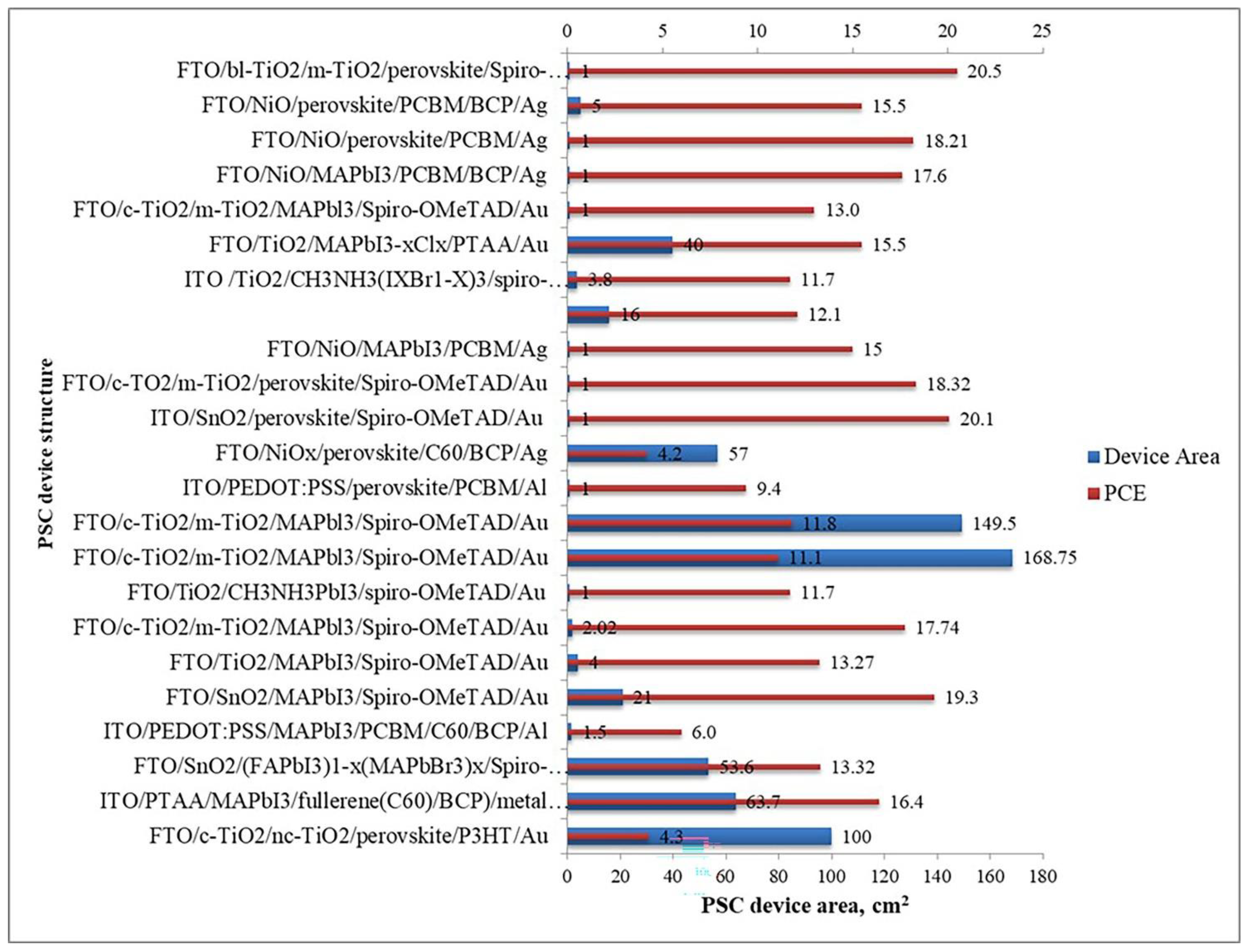
  • While the PSCs have had similar structures, the materials used (Figure 19) and device sizes have been significantly variable, thus contributing to the widespread variability in experimental results. It would be interesting to see, for example, researchers replicating the same materials if possible. Still, with different perovskite film fabrication methods, the performances of large-area PSCs of the same size can be compared in a standardized way. As it is, there is a great deal of information on PSCs, but it is rather disparate, which has the undesired outcome of delaying the universal commercialization of this important PV technology.

3. Prospects for Large-Area PSC Thin Film Fabrication Methods

Senthil and Kalaiselvi suggest that drop-casting is a potentially scalable fabrication method for PSCs films [154]. Drop casting is analogous to spin coating, with the main difference being that substrate spinning is unnecessary, and there is improved utilization of materials. The resultant film thickness can be controlled by varying the dispersion volume and the particle concentration, but the solvents should be volatile and readily wet the substrate. The major advantage of drop-casting is that it is a fast and cheap method to produce thin films on large substrates. The major disadvantage of drop-casting is the difficulty of having a uniform evaporation rate across the substrate, which causes discrepancies in film thickness and crystallinity. This method has been utilized in the past with the pioneering application for perovskite thin-film reported in 2013, but has not been used much in recent years [42].
Other methods that could find application for PSC thin film fabrication in the near future include electrospray deposition, the sol–gel technique, and the molecular precursor method (MPM). These three methods are relatively new compared to the other methods discussed earlier and noted by Philipus et al., who are active in research areas in the thin-film fabrication of energy materials [155]. However, MPM is the most promising of the three considering that it can be readily integrated with established fabrication methods such as spin coating and spray coating. Furthermore, MPM thin films of metal oxides require low annealing temperatures compared to the sol–gel method and have been shown to have much finer crystals with better uniformity. The graphic timeline on thin-film fabrication methods for inorganic and hybrid halide perovskites developed by [42] shows that in the previous five years, researchers have mainly applied solution-based methods in the fabrication of PSCs, as shown in Figure 3. These methods are slot-die coating, ink-jet printing, blade coating, spray coating, and spin coating. Co-evaporation and single source-vacuum deposition are the only vacuum-based deposition methods that have been used recently in PSC thin film fabrication. The same authors point out that ink-jet printing, blade coating, spray coating, and slot-die coating are capable of surmounting the challenges in the fabrication of large-area PSCs; for example, ensuring the scalability and uniformity of deposits across the device. Therefore, if there are to be quick innovations in fabrication methods for PSC thin films, the focus should be on these solution-based methods. Furthermore, these innovations can be small optimizations or incremental steps since the methods have successfully produced PSCs of high PCE.

Flexible PSCs

There is heightened research activity in the area of flexible PSCs, which has yielded high-performing cells with the added advantage of light weight [154]. Flexible solar cell technology is driven by the pursuit of inexpensive mass production and thin, lightweight PV modules to enhance the integration of solar cells on any surface or structure, whether rigid, curved, or flexible, for portable and indoor electronic devices. These authors credit the development of various low-temperature methods that have been developed for fabricating high-performing electronic selective layers to the fact that flexible PSCs are constructed of flexible substrates such as polyethylene terephthalate, which cannot be processed at temperatures exceeding 200 °C. The high efficiency of flexible PSCs results from the low-temperature electronic selective layers and the high-quality perovskite absorber characteristics that include grain size, trap density, charge transport, and carrier lifespan. Nevertheless, compared to rigid PSCs, flexible PSCs have much lower PCEs despite being fabricated through similar deposition processes for the perovskite absorber film. Thus, innovative deposition methods are necessary to attain high PCEs of perovskite films, particularly for large-area flexible PSCs. The quality of the perovskite film for flexible PSCs can be upgraded considerably by incorporating an additive dimethyl sulfide into the perovskite precursor solution, which refines the grain size and crystallinity. This is how the highest reported PCE of 18.40% for flexible PSCs was attained, and it is anticipated that large area flexible PSCs can attain a PCE of 13.35% [156].

4. Strategies to Improve the PCE of Large-Area PSCs

The PSC device performance is generally affected by moisture, oxygen, temperature, and illumination. Therefore, many researchers have developed significant technologies to improve the PCEs of large-area PSC devices. The first method is the modification of perovskite’s chemical composition, including solvent engineering [157], interfacial engineering, bandgap engineering [157,158,159,160], bandgap adjustment, and the increasing of the charge generation [54,78,145]. The second method is the enlargement of perovskite’s grain size [95,98,122,161]. The third method involves modifying the interface [2,162,163,164,165], which reduces interface contact, resistance interface, and surface recombination and increases the short-circuit current [145,166]. Asghar et al. included additives in layers, charge-selective contacts, interfaces (ETL perovskite and HTL perovskite), fabrication methods, and electrical biasing [167].

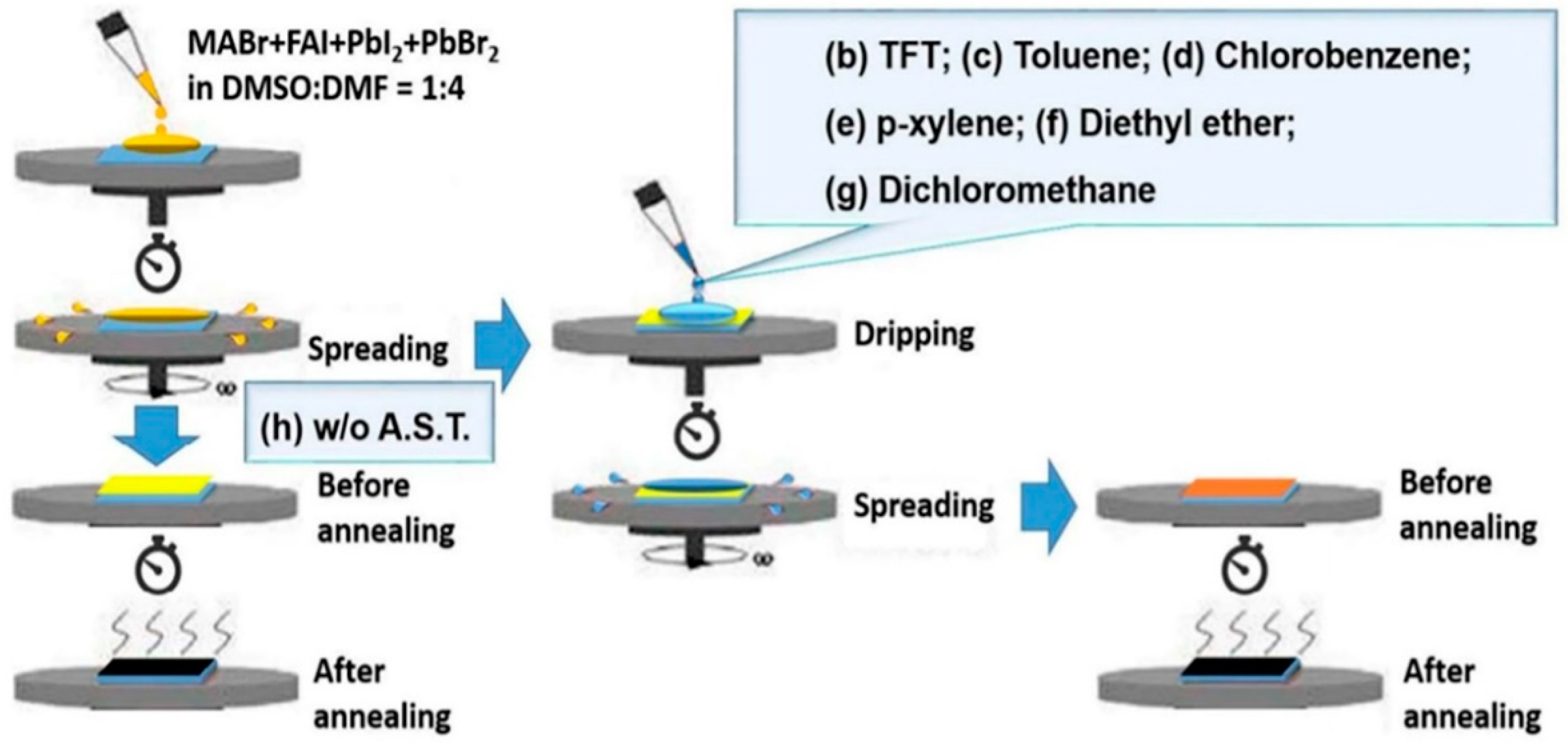
4.1. Solvent Engineering

Solvent engineering is regarded as the most prevalent method applied in one-step deposition processes. Paek et al. established an antisolvent deposition method built on one-step spin coating [168], which consists of dripping a non-coordinate solvent such as toluene onto the perovskite film while spinning; this is presented in Figure 20. This method produces tremendously smooth and uniform perovskite films. These researchers achieved PSCs with a PCE of 20.3% using trifluorotoluene as the antisolvent. However, this method is hindered by the toxicity and high cost of trifluorotoluene, toluene, and chlorobenzene in mass production. A non-toxic and low-priced antisolvent is essential to regulate the perovskite crystallization process in order to produce superior quality films and controllable morphologies [168].
Huang et al. established a technique for the rapid development and crystallization of perovskite films by adding hydrobromic acid to the perovskite precursor solutions. In this scenario, the halogen ion and a substantial donor can interact strongly with Pb2+ to form a uniform solution, which facilitates the rapid growth of high-quality perovskite films. The addition of HBr reduced the crystallization time. The fabricated PSCs had lesser current leakages and improved surface coverage, resulting in a mean PCE of 15.76% [169]. Nevertheless, the perovskite film grains were still small and not compact enough to attain higher PCEs. Gao et al. added formamidine acetate salt to the perovskite precursor solutions to enhance the perovskite film crystal quality and morphology. These authors fabricated highly homogeneous perovskite films with low trap states and uniform morphologies, using 5 mol% formamidine acetate. The resultant cells achieved a mean PCE of 18.90%, corresponding to a 3.0% improvement in the PCE over those doped with HBr. It was also proven that formamidine acetate can successfully improve perovskite’s film morphology and crystalline quality, leading to high PSC performance [170]. Additive engineering is a widespread method that is appropriate for many perovskite deposition methods.
Wang et al. utilized a one-step anti-solvent deposition method utilizing diisopropyl ether as a dripping solvent to produce highly uniform and crystalline CH3NH3PbI3 perovskite films. PSCs produced through the antisolvent deposition method with diisopropyl ether solvent had an average PCE of 17.67% and a highest PCE of 19.07% [171] compared to perovskite films fabricated using toluene, chlorobenzene, or chloroform. Therefore, diisopropyl ether is the most appropriate solvent for the antisolvent deposition method.
Rai et al. introduced the one-and-a-half step deposition method for mixed-cation perovskites molded in a submicron-sized grid structure for semi-transparent PSCs. The preliminary perovskite phase is formed in one step using the grid pattern. The next step involves immersing the pre-deposited perovskite grid into a hot solution of FAI in isopropanol. The second step improves the pore filling, crystal quality, and size. It also decreases the amount of left-over PbI2 and improves the PSC photophysical properties. An average PCE of 10% was attained with a gold contact for the best semi-transparent solar cell made using this innovation by these researchers [172].
Yang et al. discussed a method for depositing high-quality FAPbI3 films with crystallization via the direct intramolecular exchange of DMSO molecules introduced in PbI2-FAI. This method yields FAPbI3 films with (111)-preferred crystallographic orientations, coarse-grained compact microstructures, and even surfaces devoid of residual PbI2 [142]. The FAPbI3-based PSCs that were fabricated yielded a maximum PCE greater than 20%.
Incorporating caesium into perovskite precursor solutions results in triple-cation perovskite compositions that have better thermal stability, fewer phase impurities [173,174], and are less affected by the fluctuating temperatures of the variable surroundings, solvent vapors, and heating protocols. These traits are needed for the commercialization of PSCs. Saliba et al. demonstrated the utilization of three cations, Cs, MA, and FA, and fabricated triple-cation perovskites of the generic form Csx(MA0.17FA0.83)(100−x)Pb(I0.83Br0.17)3. This method enables more reproducible device performances, reaching the highest stable PCE of 21.1% [175].
PSCs in which Br was added to the mixed halide displayed improved stability after 30 days, while PCE in cells without Br dropped by 20% from the initial. The equimolar Br/I devices produced a PCE improvement of 37%. This jump in PCE may have resulted from the rearrangement of PSCs’ 3D conformation over time [176,177]. Based on these methods, high-quality perovskite films with good morphology can be obtained through solvent processing by the following means: applying sophisticated engineering of the solvent, varying the annealing temperature, adjusting the processing additives, and annealing the solvent [21,178]. Additives such as arsenic are commonly introduced into perovskite precursor solutions to improve film crystallinity.
First-rate (defect and pinhole-free) large-area perovskite film is required for PSCs to achieve high PCEs because the defects and pinholes result in electrical leakage, decreasing the Voc and FF and reducing the PCE. Kim et al. established a one-step spin-coating method that utilizes a high temperature and short-time annealing (HTSA) process and produced pinhole-free perovskite films with grain sizes >1 mm. These authors obtained PCEs of 18.32% with HTSA-400 °C and 13.56% with HTSA-100 °C on a 1 cm2 PSC device [151]. Grätzel et al. used the VAS method to manufacture perovskite films, producing perovskite films with grain sizes of 400 to 1000 nm. The PSC device fabricated and tested by Grätzel et al. had an aperture area exceeding 1 cm2 and a certified PCE of 19.6% [17]. Zhou et al. used an MA gas treatment to generate smooth, homogeneous, and full coverage MAPbI3 perovskite films [179]. A PCE increase from 5.7% to 15.1% was observed, which resulted from improved film morphology.
A notable advance was made using MAPbI3 perovskite nanocrystals as light absorbers to manufacture a solid-state mesoporous PSC with a peak PCE of 9.7% [180]. Etgar et al. synthesized a high-performance hole-transport, material-free TiO2/MAPbI3/Au PSC with a PCE of 10.49% [181], while Snaith’s group developed a planar thin-film PSC with a PCE of 12.3% [173,174]; the PCE improved to 17.9% and then to 20.1% [142]. These authors also reported on an ambient and solution-processable ionic liquid, [BMIM]BF4, used as a protective layer and an active electron modification coating for the production of high-performance PSCs. Additionally, the authors reported a remarkable PCE of 19.30% at 1 sun illumination and a record-setting indoor PCE of 35.20% (active area of 9 mm2), the highest PCE recorded for indoor PSCs [20,182,183].

4.2. Interfacial Engineering

This method can enhance interface contact, alleviate charge carrier recombination, and intensify carrier collection, which are significant to achieving high-performance and high-stability PSCs [20,54,184,185]. Interface engineering comprises doped plasma etching, self-assembled monolayers, and an interface buffer layer. Doping improves the electrical performance of the charge transport layers, enhancing carrier concentration and movement [15,183,186,187].
Notably, many researchers have demonstrated the efficiency of interfacial engineering as a strategy to eliminate amorphous structures and suppress the hysteresis of PSCs. Around half of all publications on thermally evaporated PSCs do not report on the presence of hysteresis and do not present J–V characteristics scanned in all voltage directions. Interfacial engineering serves as a means of passivation of interfacial defects and suppression of ion migration or interfacial reactions [149].

4.3. Bandgap Engineering

Ergen et al. produced a novel PSC design that attained a steady-state average PCE of 18.4%, with a best steady-state PCE of 21.7% and a peak PCE of 26% [188]. This innovative PSC had a one-atom-thick layer of hexagonal boron nitride and combined two mixtures of perovskite materials in a high-performance, graded bandgap tandem solar cell. The first mixture was constituted of methyl, ammonia, tin, and iodine, whereas the second mixture contained lead and iodine doped with bromine. The first mixture was graded to absorb 1 eV infrared light, while the latter absorbed 2 eV photons [11].
Grätzel et al. utilized Mg-Li co-doped NiO as HTL and Nb-doped TiOx as an ETL material to fabricate a large-area PSC, as shown in Figure 21a, and achieved a PCE of 15% [152]. Figure 21b shows a cross-sectional SEM image of the device, and the band alignments of related functional layers are shown in Figure 21c. Chemical molecular engineering of the perovskite materials can be used to control the bandgap of the perovskite film and achieve an ideal bandgap that is needed in PSCs for high PCEs.

5. Future Perspectives on the Synthesis and Commercialization of Large-Area PSCs

PSCs can be easily manufactured at a lower cost compared to standard solar cells [10,22,23,24,189,190]. Hence, increased research on the scalable manufacture and commercialization of large-area PSCs is envisaged. Most PSC perovskite film fabrication will likely be conducted using blade coating, slot-die coating, and ink-jet printing, as observed by [34,36], because solution processing technology represents the lowest-cost production method for thin-film PSCs [7]. While these methods are well established (not only for PSC production), research efforts could also be targeted at driving down the PSC production costs associated with these methods; for example, ink wastage associated with ink-jet printing.
Saule Technologies has commercialized building-integrated photovoltaic PSCs, electric vehicle charging ports, and PSCs for Internet of Things (IoT) applications. BIPV is one of the rapidly developing segments of the photovoltaic industry and current global climate action as espoused by the 26th United Nations Climate Change Conference of the Parties (COP26) of 31 October 13 November 2021. One goal of COP26 is to secure global net-zero carbon emissions by 2050 and keep a 1.5 °C increase in average global surface temperature within reach. Reducing the energy consumption of buildings is one of the ways to achieve net-zero, and PSC BIPVs could be one of the cheapest solutions in the medium to long term. Therefore, it is plausible to expect more companies to come on board and produce similar plus other PSC-based products. There will likely be a more significant financial investment in commercial PSC manufacturing by individuals, corporations, and governments as more climate finance is available to fight the effects of climate change and help achieve net-zero. By and large, PSCs and module failure modes are very much a black box despite the rapid degradation and poor stability associated with these devices. Predictably, there could be problems with the first generation of commercial PSC products, which will only be encountered after wide-scale and long-term usage. This will spur more research and development efforts and grow the PSC industry to resolve those issues.
It is expected that ongoing research to improve PSC performance and stability will continue. These two aspects are also critical for the commercialization of these photovoltaic cells, and several studies [95,160,161,165] have exploited the various opportunities for increasing the PCE and stability of PSCs. These opportunities include optimizing solvent processing and engineering, varying the annealing temperature, adjusting the processing additives, and annealing the solvent [21,178].
Nevertheless, there are three main obstacles to the full commercialization of PSCs. First, the poor stability of the perovskite material needs to be addressed for long-lasting, stable power output. Second, the harmful Pb2+ waste and pollution [191,192] generated by the perovskite materials’ irreversible degradation need to be constrained and managed. This calls for increased research and development focused on the maximization of the stability and the minimization of the environmental impact of current commercial PSC technology. Third, the PSCs’ performance needs to be enhanced to fulfill the needs of industrial-scale fabrication and real-life applications. It is possible to use valence state replacement to select suitable non-toxic elements using first-principle-based calculation to meet these challenges. As shown in Figure 22, the Pb element can be replaced with either homovalent elements such as Sn, Ge, and Cu or heterovalent elements such as Sb and Bi [193].
Apart from Saule Technologies, two other photovoltaics manufacturing companies producing commercial large-area PSCs are the United Kingdom-based Oxford PV and Microquanta Semiconductor based in Hangzhou, China. Oxford PV is integrating perovskites into combined perovskite–silicon cells with PCEs as high as 29.5%. The PCEs of Oxford PV far surpass the 10% reached by Saule Technologies’ PSCs, which are much cheaper to produce. On the other hand, Microquanta Semiconductor manufactures rigid solar panels composed of perovskite cells encapsulated in glass (https://www.technologyreview.com/2021/06/29/1027451/perovskite-solar-panels-hype-commercial-debut, accessed on 8 February 2022). This illustrates that different manufacturers will opt for different approaches in the synthesis and commercialization of PSCs, and obviously, the products will cater for different needs and markets. It is highly probable that any company that ventures into the commercial manufacturing of PSCs will adopt one of the three concepts discussed here or will develop concepts that are more or less derivatives of these three.
Research on lead-free PSCs is expected to rapidly advance to meet commercial development needs. Metal-halide-based perovskites, specifically Bi, Sb, and their derivatives, are becoming increasingly important [194]. Bi is a non-toxic element with comparable characteristics and ionic radius to Pb and has consequently been used to substitute Pb in PSCs. Bi-based perovskite materials have good stability, supported by the tolerance factor’s stability prediction. These materials also possess high absorption coefficients, which are synonymous with excellent sunlight absorption in photovoltaic applications. Some studies have used Bi as an encapsulation layer on lead–halide PSCs to stem corrosion [195], but this does not solve the toxicity problem.
Some researchers have enhanced the bandgaps and absorption abilities of bismuth perovskites by modifying the chemical composition of the starting materials [196]. These chemical composition modifications warrant further studies, bearing in mind that bismuth perovskites could be what the industry needs to successfully commercialize PSCs. The photovoltaic performance and comprehensive experimental defect characterization of lead-free perovskites such as Bi perovskites [197,198] have not been studied, meaning there are insufficient data on such PSCs for large-area fabrication. Subsequently, the expectation is for more studies on these topics with the aim of commercially fabricating lead-free, large-area PSCs.
A recent SciVal Research Area Trends Report on Bismuth Perovskites lists a few scholarly publications on bismuth perovskites, illustrating the infancy of this PSC study area [199]. Thus, the next few years could see a spike in the number of studies and scholarly output on the fabrication of large-area Bi-halide perovskites and attendant issues such as stability, surface deposit morphology, PCE, and other photovoltaic applications for lead-free perovskites.

6. Conclusions

This paper reviewed several scalable fabrication methods available for the commercial production of perovskite thin films for large-area PSCs. The methods discussed were spray coating, slot-die coating, blade coating, ink-jet printing, vacuum flash-assisted solution, chemical vapor deposition, sequential evaporation, co-evaporation, flash-evaporation, vacuum thermal evaporation, and multi-flow air knife. These methods have different costs and produce perovskite layers of varying quality (homogeneity, morphology, and thickness gauge), stability, and PCE. Since a scalable fabrication method’s critical requirement is low cost, vacuum-based methods could be dismissed based on vacuum technology’s high cost; however, several trade-offs need to be considered. As reported in this paper, several innovations aim to improve PSCs’ PCE. These innovations target the modification of perovskite’s chemical composition, the improvement of perovskite’s film quality, as well as interface engineering.
Regarding all the methods reviewed in this paper, blade coating, slot-die coating, and ink-jet printing offer the most attractive prospects for the scalable manufacture of large-area PSCs with high PCEs. Blade coating is relatively simple compared to the other single-directional coating methods and has the most adjustable cost-effective deposition tunable to a specific application. Slot-die coating demonstrated the highest PCEs for large-area PSCs in recent publications. Ink-jet printing allows for direct modelling of the printed layers, enables modified complex cell geometries for specific applications, and offers rapid turnover. The choice of a fabrication method for the scalable manufacture of large-area PSCs with high PCEs is difficult. Still, the three methods discussed here are all solution-based instead of vapor deposition methods, which should simplify the choice. Improvements in the process parameters of these fabrication methods have been shown to improve the PCEs of PSCs and the perovskite film quality. For instance, inkjet printing advances in printing parameters, such as speed and ink–substrate separation distance, have produced good results in small-area PSCs at the laboratory scale. If these successes can be translated to large-area PSCs, and the toxicity and stability issues of halide perovskites are solved, then universal commercialization of PSCs can be realized. PSCs have a high potential to achieve low-cost production compared to the conventional photovoltaic technology that needs high energy and vacuum to prepare solar cells. The interchange between the low cost and high performance of PSCs is a critical issue that must be considered in device intensification. The only company that has started commercial production and marketing of PSC photovoltaic devices has suppressed production costs by utilizing ink-jet printing, but the trade-off has been a modest PCE of 10%. However, other manufacturers, scientists, researchers, energy experts, and consumers might have a dim view of that sacrifice in photovoltaic performance. After all, are PV cells not meant to harness as much solar energy as possible?

Author Contributions

Conceptualization, Methodology, Writing—review and editing, and submission of the manuscript to this journal S.L.H.; Supervision, H.H. and Z.Z.; Writing—review and editing, and visualization; M.M.M.; Visualization and Methodology: J.D. and L.H.; Validation, T.Z. and J.X. All authors have read and agreed to the published version of the manuscript.

Funding

This work was financially supported by the Open Foundation of the Key Laboratory of Semiconductor Materials Science, Institute of Semiconductors, Chinese Academy of Sciences (No. KLSMS-1901).

Data Availability Statement

All data generated or analyzed during this study are included in this published article.

Conflicts of Interest

The authors declare that they have no known competing financial interests or personal relationships that could have appeared to influence the work reported in this paper. The funders had no role in the design of the study; in the collection, analyses, or interpretation of data; in the writing of the manuscript, or in the decision to publish the results.

Abbreviations

PSCsPerovskite Solar Cells
PSCPerovskite Solar Cell
PVPhotovoltaic
ETMsElectron Transport Materials
HTMsHole Transport Materials
HTLHole Transport Layer
ETLElectron Transport Layer
SEMScanning Electron Microscope
TCOTransparent Conductive Oxide
FTOFluorine-doped Tin Oxide
PCEPower Conversion Efficiency
EQEExternal Quantum Efficiency
NRELNational Renewable Energy Laboratory
CVDChemical Vapor Deposition
MAIMethylammonium Iodide
FAIFormamidinium Iodide
DMSODimethyl Sulfoxide
DMFN, N-dimethylformamide
GBLGamma-butyrolactone
HIHydrogen Iodide
CNTsCarbon Nanotubes
I–VCurrent–Voltage
J–VCurrent Density–Voltage
VocOpen-Circuit Voltage
JscShort Circuit Current
FFFill Factor
VASVacuum Flash-Assisted Solution
VASPVacuum Flash-Assisted Solution Processing
MAKMulti-Flow Air Knife
HTSAHigh temperature and short-time annealing
MPMMolecular Precursor Method
µLMicroliter
Spiro-OMeTADC81H68N4O8
CuCopper
InIndium
GaGallium
SeSelenium
CdCadmium
TeTellurium
GBL-DMSOGamma-Butyrolactone Dimethyl Sulfoxide
BIPVsBuilding-Integrated Photovoltaics
IoTInternet of Things

References

  1. Kour, R.; Arya, S.; Verma, S.; Gupta, J.; Bandhoria, P.; Bharti, V.; Datt, R.; Gupta, V. Potential Substitutes for Replacement of Lead in Perovskite Solar Cells: A Review. Glob. Chall. 2019, 3, 1900050. [Google Scholar] [CrossRef] [PubMed] [Green Version]
  2. Rajagopal, A.; Yao, K.; Jen, A.K.Y. Toward Perovskite Solar Cell Commercialization: A Perspective and Research Roadmap Based on Interfacial Engineering. Adv. Mater. 2018, 30, 1800455. [Google Scholar] [CrossRef] [PubMed]
  3. Enriquez, C.; Hodges, D.; De La Rosa, A.; Valerio Frias, L.; Ramirez, Y.; Rodriguez, V.; Rivera, D.; Telle, A. Perovskite Solar Cells. In Proceedings of the 2019 IEEE 46th Photovoltaic Specialists Conference (PVSC), Chicago, IL, USA, 16–21 June 2019. [Google Scholar] [CrossRef]
  4. Hamukwaya, S.L.; Zhao, Z.; Wang, N.; Liu, H.; Umar, A.; Zhang, J.; Wu, T.; Guo, Z. Enhanced Photocatalytic Activity of B, N-Codoped TiO2 by a New Molten Nitrate Process. J. Nanosci. Nanotechnol. 2018, 19, 839–849. [Google Scholar] [CrossRef]
  5. Lewis, N.S.; Nocera, D.G. Powering the planet: Chemical challenges in solar energy utilization. Proc. Natl. Acad. Sci. USA 2006, 103, 15729–15735. [Google Scholar] [CrossRef] [PubMed] [Green Version]
  6. Wang, R.; Mujahid, M.; Duan, Y.; Wang, Z.K.; Xue, J.; Yang, Y. A Review of Perovskites Solar Cell Stability. Adv. Funct. Mater. 2019, 29, 1808843. [Google Scholar] [CrossRef]
  7. Li, D.; Shi, J.; Xu, Y.; Luo, Y.; Wu, H.; Meng, Q. Inorganic-organic halide perovskites for new photovoltaic technology. Natl. Sci. Rev. 2018, 5, 559–576. [Google Scholar] [CrossRef] [Green Version]
  8. Niu, G.; Guo, X.; Wang, L. Review of recent progress in chemical stability of perovskite solar cells. J. Mater. Chem. A 2015, 3, 8970–8980. [Google Scholar] [CrossRef]
  9. Parisi, M.L.; Maranghi, S.; Basosi, R. The evolution of the dye sensitized solar cells from Grätzel prototype to up-scaled solar applications: A life cycle assessment approach. Renew. Sustain. Energy Rev. 2014, 39, 124–138. [Google Scholar] [CrossRef]
  10. Uddin, A.; Upama, M.B.; Yi, H.; Duan, L. Encapsulation of organic and perovskite solar cells: A review. Coatings 2019, 9, 65. [Google Scholar] [CrossRef] [Green Version]
  11. Tang, H.; He, S.; Peng, C. A Short Progress Report on High-Efficiency Perovskite Solar Cells. Nanoscale Res. Lett. 2017, 12, 410. [Google Scholar] [CrossRef]
  12. Wang, F.; Cao, Y.; Chen, C.; Chen, Q.; Wu, X.; Li, X.; Qin, T.; Huang, W. Materials toward the Upscaling of Perovskite Solar Cells: Progress, Challenges, and Strategies. Adv. Funct. Mater. 2018, 28, 1803753. [Google Scholar] [CrossRef]
  13. Pitchaiya, S.; Natarajan, M.; Santhanam, A.; Asokan, V.; Yuvapragasam, A.; Madurai Ramakrishnan, V.; Palanisamy, S.E.; Sundaram, S.; Velauthapillai, D. A review on the classification of organic/inorganic/carbonaceous hole transporting materials for perovskite solar cell application. Arab. J. Chem. 2020, 13, 2526–2557. [Google Scholar] [CrossRef]
  14. Assadi, M.K.; Bakhoda, S.; Saidur, R.; Hanaei, H. Recent progress in perovskite solar cells. Renew. Sustain. Energy Rev. 2018, 81, 2812–2822. [Google Scholar] [CrossRef]
  15. Chen, Y.; Zhang, L.; Zhang, Y.; Gao, H.; Yan, H. Large-area perovskite solar cells-a review of recent progress and issues. RSC Adv. 2018, 8, 10489–10508. [Google Scholar] [CrossRef] [Green Version]
  16. Zhao, Y.; Ma, F.; Gao, F.; Yin, Z.; Zhang, X.-W.; You, J. Research Progresses in Large-Area Perovskite Solar Cells. Photonics Res. 2020, 8, A1–A15. [Google Scholar] [CrossRef]
  17. Li, X.; Bi, D.; Yi, C.; Décoppet, J.D.; Luo, J.; Zakeeruddin, S.M.; Hagfeldt, A.; Grätzel, M. A vacuum flash-assisted solution process for high-efficiency large-area perovskite solar cells. Science 2016, 353, 58–62. [Google Scholar] [CrossRef]
  18. Lee, J.W.; Lee, D.K.; Jeong, D.N.; Park, N.G. Control of Crystal Growth toward Scalable Fabrication of Perovskite Solar Cells. Adv. Funct. Mater. 2019, 29, 1807047. [Google Scholar] [CrossRef]
  19. Kim, D.H.; Whitaker, J.B.; Li, Z.; van Hest, M.F.A.M.; Zhu, K. Outlook and Challenges of Perovskite Solar Cells toward Terawatt-Scale Photovoltaic Module Technology. Joule 2018, 2, 1437–1451. [Google Scholar] [CrossRef] [Green Version]
  20. Park, N.G. Research Direction toward Scalable, Stable, and High Efficiency Perovskite Solar Cells. Adv. Energy Mater. 2020, 10, 1903106. [Google Scholar] [CrossRef]
  21. Dai, X.; Xu, K.; Wei, F. Recent progress in perovskite solar cells: The perovskite layer. Beilstein J. Nanotechnol. 2020, 11, 51–60. [Google Scholar] [CrossRef]
  22. Kim, J.; Yun, J.S.; Cho, Y.; Lee, D.S.; Wilkinson, B.; Soufiani, A.M.; Deng, X.; Zheng, J.; Shi, A.; Lim, S.; et al. Overcoming the Challenges of Large-Area High-Efficiency Perovskite Solar Cells. ACS Energy Lett. 2017, 2, 1978–1984. [Google Scholar] [CrossRef]
  23. Park, N.G.; Zhu, K. Scalable fabrication and coating methods for perovskite solar cells and solar modules. Nat. Rev. Mater. 2020, 5, 333–350. [Google Scholar] [CrossRef]
  24. Gao, F.; Zhao, Y.; Zhang, X.; You, J. Recent Progresses on Defect Passivation toward Efficient Perovskite Solar Cells. Adv. Energy Mater. 2020, 10, 1902650. [Google Scholar] [CrossRef]
  25. Dai, T.; Cao, Q.; Yang, L.; Aldamasy, M.H.; Li, M.; Liang, Q.; Lu, H.; Dong, Y.; Yang, Y. Strategies for High-Performance Large-Area Perovskite Solar Cells toward Commercialization. Crystals 2021, 11, 295. [Google Scholar] [CrossRef]
  26. Niu, T.; Zhu, W.; Zhang, Y.; Xue, Q.; Jiao, X.; Wang, Z.; Xie, Y.M.; Li, P.; Chen, R.; Huang, F.; et al. D-A-π-A-D-type Dopant-free Hole Transport Material for Low-Cost, Efficient, and Stable Perovskite Solar Cells. Joule 2021, 5, 249–269. [Google Scholar] [CrossRef]
  27. Li, Z.; Klein, T.R.; Kim, D.H.; Yang, M.; Berry, J.J.; Van Hest, M.F.A.M.; Zhu, K. Scalable fabrication of perovskite solar cells. Nat. Rev. Mater. 2018, 3, 18017. [Google Scholar] [CrossRef]
  28. Bae, I.G.; Park, B. All-self-metered solution-coating process in ambient air for the fabrication of efficient, large-area, and semitransparent perovskite solar cells. Sustain. Energy Fuels 2020, 4, 3115–3128. [Google Scholar] [CrossRef]
  29. Burschka, J.; Pellet, N.; Moon, S.J.; Humphry-Baker, R.; Gao, P.; Nazeeruddin, M.K.; Grätze, M. Sequential deposition as a route to high-performance perovskite-sensitized solar cells. Nature 2013, 499, 316–319. [Google Scholar] [CrossRef]
  30. Xiao, Z.; Bi, C.; Shao, Y.; Dong, Q.; Wang, Q.; Yuan, Y.; Wang, C.; Gao, Y.; Huang, J. Efficient, high yield perovskite photovoltaic devices grown by interdiffusion of solution-processed precursor stacking layers. Energy Environ. Sci. 2014, 7, 2619–2623. [Google Scholar] [CrossRef]
  31. Liu, X.; Cao, L.; Guo, Z.; Li, Y.; Gao, W.; Zhou, L. A review of perovskite photovoltaic materials’ synthesis and applications via chemical vapor deposition method. Materials 2019, 12, 3304. [Google Scholar] [CrossRef] [Green Version]
  32. Shalan, A.E. Challenges and approaches towards upscaling the assembly of hybrid perovskite solar cells. Mater. Adv. 2020, 1, 292–309. [Google Scholar] [CrossRef]
  33. Hwang, K.; Jung, Y.S.; Heo, Y.J.; Scholes, F.H.; Watkins, S.E.; Subbiah, J.; Jones, D.J.; Kim, D.Y.; Vak, D. Toward large scale roll-to-roll production of fully printed perovskite solar cells. Adv. Mater. 2015, 27, 1241–1247. [Google Scholar] [CrossRef] [PubMed]
  34. Razza, S.; Di Giacomo, F.; Matteocci, F.; Cinà, L.; Palma, A.L.; Casaluci, S.; Cameron, P.; Epifanio, A.D.; Licoccia, S.; Reale, A.; et al. Perovskite solar cells and large area modules (100 cm2) based on an air flow-assisted PbI2 blade coating deposition process. J. Power Sources 2015, 277, 286–291. [Google Scholar] [CrossRef]
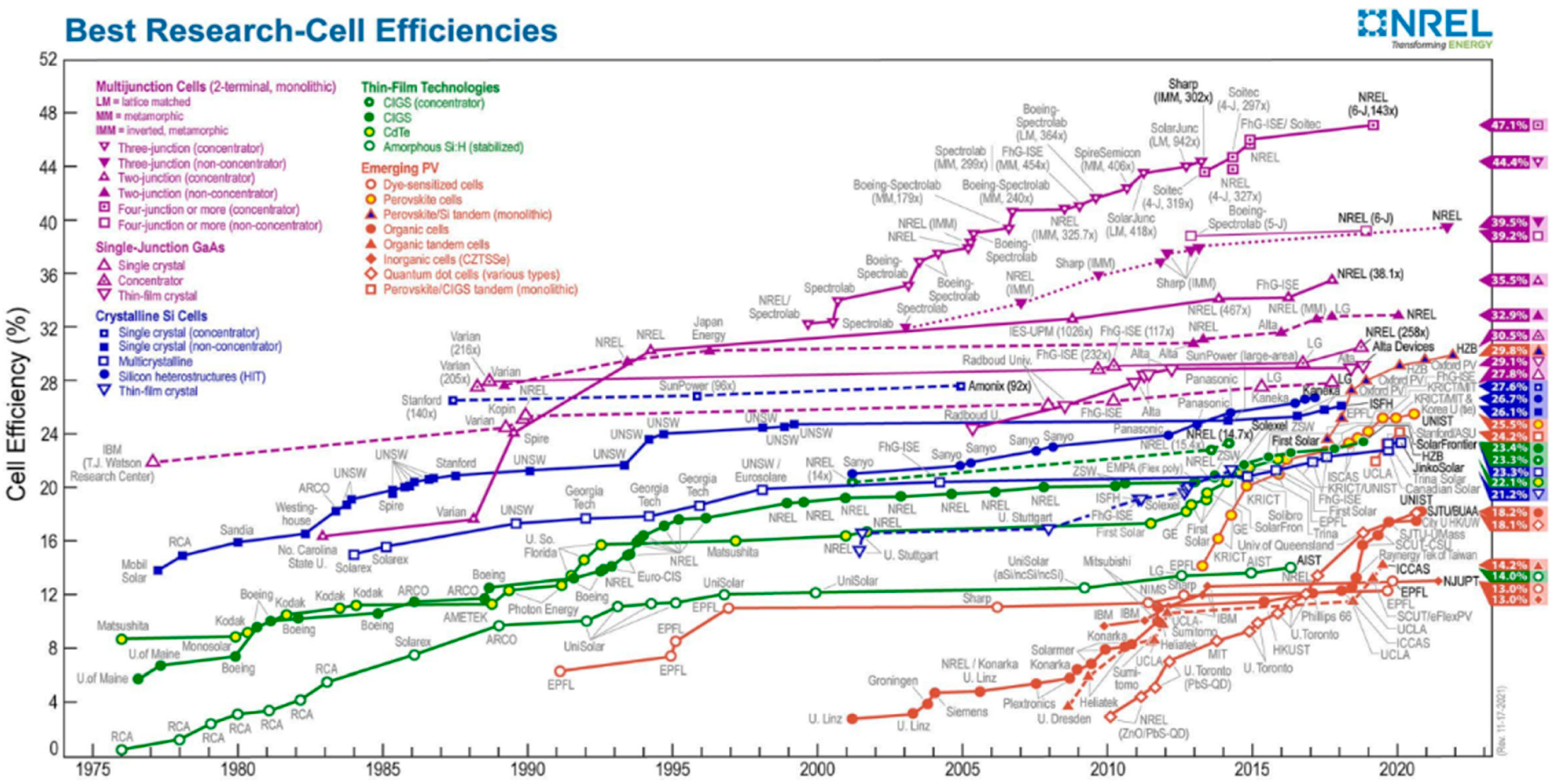
  35. NREL. Best-Research-Cell-Efficiencies-Rev211117. Available online: https://www.nrel.gov/pv/assets/pdfs/best-research-cell-efficiencies-rev211117.pdf (accessed on 22 January 2022).
  36. Zhihui Photovolt. The Efficiency of Perovskite Components Exceeds 18%, and There Is Huge Room for Imagination in the Future! 2020. Available online: Http://solar.in-en.com/html/solar-2352538.shtml (accessed on 18 January 2022).
  37. Jean, J.; Xiao, J.; Nick, R.; Moody, N.; Nasilowski, M.; Bawendi, M.; Bulović, V. Synthesis cost dictates the commercial viability of lead sulfide and perovskite quantum dot photovoltaics. Energy Environ. Sci. 2018, 11, 2295–2305. [Google Scholar] [CrossRef]
  38. Song, Z.; McElvany, C.L.; Phillips, A.B.; Celik, I.; Krantz, P.W.; Watthage, S.C.; Liyanage, G.K.; Apul, D.; Heben, M.J. A technoeconomic analysis of perovskite solar module manufacturing with low-cost materials and techniques. Energy Environ. Sci. 2017, 10, 1297–1305. [Google Scholar] [CrossRef]
  39. Zhang, Q.; Hao, F.; Li, J.; Zhou, Y.; Wei, Y.; Lin, H. Perovskite solar cells: Must lead be replaced-and can it be done? Sci. Technol. Adv. Mater. 2018, 19, 425–442. [Google Scholar] [CrossRef] [Green Version]
  40. Swartwout, R.; Hoerantner, M.T.; Bulović, V. Scalable Deposition Methods for Large-Area Production of Perovskite Thin Films. Energy Environ. Mater. 2019, 2, 119–145. [Google Scholar] [CrossRef] [Green Version]
  41. Yang, Z.; Zhang, S.; Li, L.; Chen, W. Research progress on large-area perovskite thin films and solar modules. J. Mater. 2017, 3, 231–244. [Google Scholar] [CrossRef]
  42. Soto-Montero, T.; Soltanpoor, W.; Morales-Masis, M. Pressing challenges of halide perovskite thin film growth. APL Mater. 2020, 8, 110903. [Google Scholar] [CrossRef]
  43. Borchert, J.; Milot, R.L.; Patel, J.B.; Davies, C.L.; Wright, A.D.; Martínez Maestro, L.; Snaith, H.J.; Herz, L.M.; Johnston, M.B. Large-Area, Highly Uniform Evaporated Formamidinium Lead Triiodide Thin Films for Solar Cells. ACS Energy Lett. 2017, 2, 2799–2804. [Google Scholar] [CrossRef]
  44. Malinkiewicz, O.; Yella, A.; Lee, Y.H.; Espallargas, G.M.; Graetzel, M.; Nazeeruddin, M.K.; Bolink, H.J. Perovskite solar cells employing organic charge-transport layers. Nat. Photon. 2014, 8, 128–132. [Google Scholar] [CrossRef]
  45. Larson, R.G.; Rehg, T.J. Spin Coating. In Liquid Film Coating; Chapman & Hall: Glasgow, UK, 1997. [Google Scholar] [CrossRef]
  46. Tzounis, L.; Stergiopoulos, T.; Zachariadis, A.; Gravalidis, C.; Laskarakis, A.; Logothetidis, S. Perovskite solar cells from small scale spin coating process towards roll-to-roll printing: Optical and Morphological studies. Mater. Today Proc. 2017, 4, 5082–5089. [Google Scholar] [CrossRef]
  47. Kim, M.K.; Lee, H.S.; Pae, S.R.; Kim, D.J.; Lee, J.Y.; Gereige, I.; Park, S.; Shin, B. Effects of temperature and coating speed on the morphology of solution-sheared halide perovskite thin-films. J. Mater. Chem. A 2018, 6, 24911–24919. [Google Scholar] [CrossRef]
  48. Han, G.S.; Kim, J.; Bae, S.; Han, S.; Kim, Y.J.; Gong, O.Y.; Lee, P.; Ko, M.J.; Jung, H.S. Spin-Coating Process for 10 cm × 10 cm Perovskite Solar Modules Enabled by Self-Assembly of SnO2 Nanocolloids. ACS Energy Lett. 2019, 4, 1845–1851. [Google Scholar] [CrossRef]
  49. Jeong, M.; Woo Choi, I.; Min Go, E.; Cho, Y.; Kim, M.; Lee, B.; Jeong, S.; Jo, Y.; Won Choi, H.; Lee, J.; et al. Stable perovskite solar cells with efficiency exceeding 24.8% and 0.3-V voltage loss. Science 2020, 369, 1615–1620. [Google Scholar] [CrossRef]
  50. Chiang, C.H.; Lin, J.W.; Wu, C.G. One-step fabrication of a mixed-halide perovskite film for a high-efficiency inverted solar cell and module. J. Mater. Chem. A 2016, 4, 13525–13533. [Google Scholar] [CrossRef]
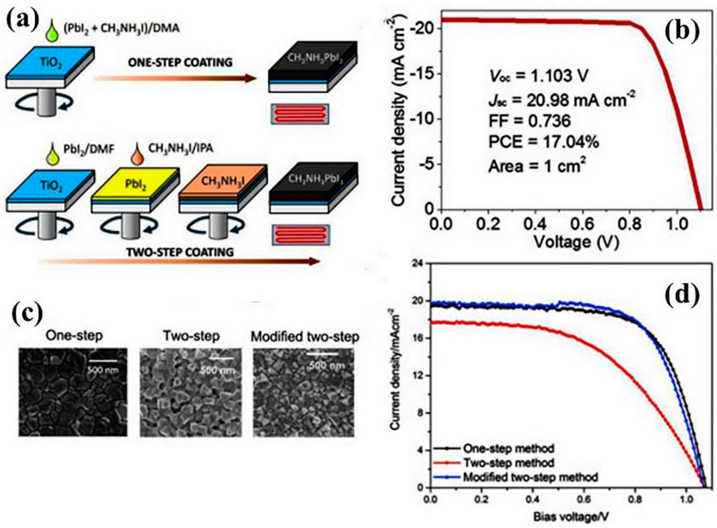
  51. Im, J.H.; Kim, H.S.; Park, N.G. Morphology-photovoltaic property correlation in perovskite solar cells: One-step versus two-step deposition of CH3NH3PbI3. APL Mater. 2014, 2, 081510. [Google Scholar] [CrossRef] [Green Version]
  52. Lee, J.; Kang, H.; Kim, G.; Back, H.; Kim, J.; Hong, S.; Park, B.; Lee, E.; Lee, K. Achieving Large-Area Planar Perovskite Solar Cells by Introducing an Interfacial Compatibilizer. Adv. Mater. 2017, 29, 1606363. [Google Scholar] [CrossRef]
  53. Jiang, Q.; Chu, Z.; Wang, P.; Yang, X.; Liu, H.; Wang, Y.; Yin, Z.; Wu, J.; Zhang, X.; You, J. Planar-structure perovskite solar cells with efficiency beyond 21%. Adv. Mater. 2017, 29, 1703852. [Google Scholar] [CrossRef]
  54. Shen, H.; Wu, Y.; Peng, J.; Duong, T.; Fu, X.; Barugkin, C.; White, T.P.; Weber, K.; Catchpole, K.R. Improved Reproducibility for Perovskite Solar Cells with 1 cm2 Active Area by a Modified Two-Step Process. ACS Appl. Mater. Interfaces 2017, 9, 5974–5981. [Google Scholar] [CrossRef]
  55. Da Silva Filho, J.M.C.; Ermakov, V.A.; Marques, F.C. Perovskite Thin Film Synthesised from Sputtered Lead Sulphide. Sci. Rep. 2018, 8, 1563. [Google Scholar] [CrossRef] [PubMed]
  56. Li, Z.; Dong, J.; Liu, C.; Guo, J.; Shen, L.; Guo, W. Surface Passivation of Perovskite Solar Cells Toward Improved Efficiency and Stability. Nano-Micro Lett. 2019, 11, 14. [Google Scholar] [CrossRef]
  57. Vidyasagar, C.C.; Muñoz Flores, B.M.; Jiménez Pérez, V.M. Recent Advances in Synthesis and Properties of Hybrid Halide Perovskites for Photovoltaics. vol. 10. SpringerOpen 2018, 10, 68. [Google Scholar] [CrossRef] [Green Version]
  58. Barrows, A.T.; Pearson, A.J.; Kwak, C.K.; Dunbar, A.D.F.; Buckley, A.R.; Lidzey, D.G. Efficient planar heterojunction mixed-halide perovskite solar cells deposited via spray-deposition. Energy Environ. Sci. 2014, 7, 2944–2950. [Google Scholar] [CrossRef]
  59. Tait, J.G.; Manghooli, S.; Qiu, W.; Rakocevic, L.; Kootstra, L.; Jaysankar, M.; Masse De La Huerta, C.A.; Paetzold, U.W.; Gehlhaar, R.; Cheyns, D.; et al. Rapid composition screening for perovskite photovoltaics via concurrently pumped ultrasonic spray coating. J. Mater. Chem. A 2016, 4, 3792–3797. [Google Scholar] [CrossRef]
  60. Das, S.; Yang, B.; Gu, G.; Joshi, P.C.; Ivanov, I.N.; Rouleau, C.M.; Aytug, T.; Geohegan, D.B.; Xiao, K. High-Performance Flexible Perovskite Solar Cells by Using a Combination of Ultrasonic Spray-Coating and Low Thermal Budget Photonic Curing. ACS Photonics 2015, 2, 680–686. [Google Scholar] [CrossRef]
  61. Yao, J.; Yang, L.; Cai, F.; Yan, Y.; Gurney, R.S.; Liu, D.; Wang, T. The impacts of PbI2 purity on the morphology and device performance of one-step spray-coated planar heterojunction perovskite solar cells. Sustain. Energy Fuels 2018, 2, 436–443. [Google Scholar] [CrossRef]
  62. Kim, H.S.; Im, S.H.; Park, N.G. Organolead halide perovskite: New horizons in solar cell research. J. Phys. Chem. C 2014, 118, 5615–5625. [Google Scholar] [CrossRef]
  63. Park, M.; Cho, W.; Lee, G.; Hong, S.C.; Kim, M.; Yoon, J.; Ahn, N.; Choi, M. Highly Reproducible Large-Area Perovskite Solar Cell Fabrication via Continuous Megasonic Spray Coating of CH3NH3PbI3. Small 2019, 15, 1804005. [Google Scholar] [CrossRef] [Green Version]
  64. Heo, J.H.; Lee, M.H.; Jang, M.H.; Im, S.H. Highly efficient CH3NH3PbI3-xClx mixed halide perovskite solar cells prepared by re-dissolution and crystal grain growth via spray coating. J. Mater. Chem. A 2016, 4, 17636–17642. [Google Scholar] [CrossRef]
  65. Siansonic. Ultrasonic and Piezoelectric Technologies. 2020. Available online: Https://www.Siansonic.Com/Products (accessed on 22 January 2022).
  66. Sono-Tek. Ultrasonic System. Available online: http://www.siansonic.com/ (accessed on 22 January 2022).
  67. Gamliel, S.; Dymshits, A.; Aharon, S.; Terkieltaub, E.; Etgar, L. Micrometer Sized Perovskite Crystals in Planar Hole Conductor Free Solar Cells. J. Phys. Chem. C 2015, 119, 19722–19728. [Google Scholar] [CrossRef]
  68. Huang, H.; Shi, J.; Zhu, L.; Li, D.; Luo, Y.; Meng, Q. Two-step ultrasonic spray deposition of CH3NH3PbI3 for efficient and large-area perovskite solar cell. Nano Energy 2016, 27, 352–358. [Google Scholar] [CrossRef]
  69. Remeika, M.; Raga, S.R.; Zhang, S.; Qi, Y. Transferrable optimization of spray-coated PbI2 films for perovskite solar cell fabrication. J. Mater. Chem. A 2017, 5, 5709–5718. [Google Scholar] [CrossRef] [Green Version]
  70. Chai, G.; Luo, S.; Zhou, H.; Daoud, W.A. CH3NH3PbI3−xBrx perovskite solar cells via spray assisted two-step deposition: Impact of bromide on stability and cell performance. Mater. Des. 2017, 125, 222–229. [Google Scholar] [CrossRef]
  71. Bishop, J.E.; Mohamad, D.K.; Wong-Stringer, M.; Smith, A.; Lidzey, D.G. Spray-cast multilayer perovskite solar cells with an active-area of 1.5 cm2. Sci. Rep. 2017, 7, 7962. [Google Scholar] [CrossRef]
  72. Ye, F.; Chen, H.; Xie, F.; Tang, W.; Yin, M.; He, J.; Bi, E.; Wang, Y.; Yang, X.; Han, L. Soft-cover deposition of scaling-up uniform perovskite thin films for high cost-performance solar cells. Energy Environ. Sci. 2016, 9, 2295–2301. [Google Scholar] [CrossRef]
  73. Wu, Y.; Yang, X.; Chen, W.; Yue, Y.; Cai, M.; Xie, F.; Bi, E.; Islam, A.; Han, L. Perovskite solar cells with 18.21% efficiency and area over 1 cm2 fabricated by heterojunction engineering. Nat. Energy 2016, 1, 16148. [Google Scholar] [CrossRef]
  74. Wu, Y.; Xie, F.; Chen, H.; Yang, X.; Su, H.; Cai, M.; Zhou, Z.; Noda, T.; Han, L. Thermally Stable MAPbI3 Perovskite Solar Cells with Efficiency of 19.19% and Area over 1 cm2 achieved by Additive Engineering. Adv. Mater. 2017, 29, 1701073. [Google Scholar] [CrossRef]
  75. Di Giacomo, F.; Fakharuddin, A.; Jose, R.; Brown, T.M. Progress, challenges and perspectives in flexible perovskite solar cells. Energy Environ. Sci. 2016, 9, 3007–3035. [Google Scholar] [CrossRef] [Green Version]
  76. Cao, K.; Zuo, Z.; Cui, J.; Shen, Y.; Moehl, T.; Zakeeruddin, S.M.; Grätzel, M.; Wang, M. Efficient screen printed perovskite solar cells based on mesoscopic TiO2/Al2O3/NiO/carbon architecture. Nano Energy 2015, 17, 171–179. [Google Scholar] [CrossRef]
  77. Li, X.; Yang, J.; Jiang, Q.; Chu, W.; Zhang, D.; Zhou, Z.; Xin, J. Synergistic Effect to High-Performance Perovskite Solar Cells with Reduced Hysteresis and Improved Stability by the Introduction of Na-Treated TiO2 and Spraying-Deposited CuI as Transport Layers. ACS Appl. Mater. Interfaces 2017, 9, 41354–41362. [Google Scholar] [CrossRef] [PubMed]
  78. Yang, W.S.; Park, B.-W.W.; Jung, E.H.; Jeon, N.J.; Kim, Y.C.; Lee, D.U.; Shin, S.S.; Seo, J.; Kim, E.K.; Noh, J.H.; et al. Iodide management in formamidinium-lead-halide-based perovskite layers for efficient solar cells. Science 2017, 356, 1376–1379. [Google Scholar] [CrossRef] [PubMed] [Green Version]
  79. Chen, H.; Ye, F.; Tang, W.; He, J.; Yin, M.; Wang, Y.; Xie, F.; Bi, E.; Yang, X.; Grätzel, M.; et al. A solvent-and vacuum-free route to large-area perovskite films for efficient solar modules. Nature 2017, 550, 92–95. [Google Scholar] [CrossRef]
  80. Lu, J.; Jiang, L.; Li, W.; Li, F.; Pai, N.K.; Scully, A.D.; Tsai, C.M.; Bach, U.; Simonov, A.N.; Cheng, Y.B.; et al. Diammonium and Monoammonium Mixed-Organic-Cation Perovskites for High Performance Solar Cells with Improved Stability. Adv. Energy Mater. 2017, 7, 1700444. [Google Scholar] [CrossRef]
  81. Jiang, Y.; Leyden, M.R.; Qiu, L.; Wang, S.; Ono, L.K.; Wu, Z.; Juarez-Perez, E.J.; Qi, Y. Combination of Hybrid CVD and Cation Exchange for Upscaling Cs-Substituted Mixed Cation Perovskite Solar Cells with High Efficiency and Stability. Adv. Funct. Mater. 2018, 28, 1703835. [Google Scholar] [CrossRef]
  82. Matteocci, F.; Cinà, L.; Di Giacomo, F.; Razza, S.; Palma, A.L.; Guidobaldi, A.; D’Epifanio, A.; Licoccia, S.; Brown, T.M.; Reale, A.; et al. High efficiency photovoltaic module based on mesoscopic organometal halide perovskite. Prog. Photovolt. Res. Appl. 2016, 24, 436–445. [Google Scholar] [CrossRef]
  83. Kim, A.; Lee, H.; Kwon, H.C.; Jung, H.S.; Park, N.G.; Jeong, S.; Moon, J. Fully solution-processed transparent electrodes based on silver nanowire composites for perovskite solar cells. Nanoscale 2016, 8, 6308–6316. [Google Scholar] [CrossRef]
  84. Khoa, N.H.; Tanaka, Y.; Goh, W.P.; Jiang, C. A solution processed Ag-nanowires/C60 composite top electrode for efficient and translucent perovskite solar cells. Sol. Energy 2020, 196, 582–588. [Google Scholar] [CrossRef]
  85. Han, K.; Xie, M.; Zhang, L.; Yan, L.; Wei, J.; Ji, G.; Luo, Q.; Lin, J.; Hao, Y.; Ma, C.Q. Fully solution processed semi-transparent perovskite solar cells with spray-coated silver nanowires/ZnO composite top electrode. Sol. Energy Mater. Sol. Cells 2018, 185, 399–405. [Google Scholar] [CrossRef]
  86. Dou, Y.; Liu, Z.; Wu, Z.; Liu, Y.; Li, J.; Leng, C.; Fang, D.; Liang, G.; Xiao, J.; Li, W.; et al. Self-augmented ion blocking of sandwiched 2D/1D/2D electrode for solution processed high efficiency semitransparent perovskite solar cell. Nano Energy 2020, 71, 104567. [Google Scholar] [CrossRef]
  87. Habibi, M.; Rahimzadeh, A.; Bennouna, I.; Eslamian, M. Defect-Free Large-Area (25 cm2) Light Absorbing Perovskite Thin Films Made by Spray Coating. Coatings 2017, 7, 42. [Google Scholar] [CrossRef] [Green Version]
  88. David, L.; Erick, C. Transparent Conductive Materials: Materials, Synthesis, Characterization, Applicationsitle; John Wiley Sons: Hoboken, NJ, USA, 2018; Volume 2, pp. 105–131. ISBN 978-3-527-80461-0. [Google Scholar]
  89. Ding, X.; Liu, J.; Htal, T.A.L. A review of the operating limits in slot die coating processes. AIChE J. 2016, 62, 2508–2524. [Google Scholar] [CrossRef]
  90. Whitaker, J.B.; Hoe Kim, D.; Larson, B.W.; Zhang, F.; Berry, J.J.; FAM van Hest, M.F.A.; Zhu, K. Scalable Slot-die Coating of High Performance Perovskite Solar Cells. Sustain. Energy Fuels 2018, 2, 2442–2449. [Google Scholar] [CrossRef]
  91. Zhao, Y.; Zhu, K. CH3NH3Cl-assisted one-step solution growth of CH3NH3PbI3, Structure, charge-carrier dynamics, and photovoltaic properties of perovskite solar cells. J. Phys. Chem. C 2014, 118, 9412–9418. [Google Scholar] [CrossRef]
  92. Zuo, C.; Vak, D.; Angmo, D.; Ding, L.; Gao, M. One-step roll-to-roll air processed high efficiency perovskite solar cells. Nano Energy 2018, 46, 185–192. [Google Scholar] [CrossRef]
  93. Di Giacomo, F.; Shanmugam, S.; Fledderus, H.; Bruijnaers, B.J.; Verhees, W.J.H.; Dorenkamper, M.S.; Veenstra, S.C.; Qiu, W.; Gehlhaar, R.; Merckx, T.; et al. Up-scalable sheet-to-sheet production of high efficiency perovskite module and solar cells on 6-in. substrate using slot die coating. Sol. Energy Mater. Sol. Cells 2018, 181, 53–59. [Google Scholar] [CrossRef]
  94. Gao, L.; Huang, K.; Long, C.; Zeng, F.; Liu, B.; Yang, J. Fully slot-die-coated perovskite solar cells in ambient condition. Appl. Phys. A Mater. Sci. Process 2020, 126, 452. [Google Scholar] [CrossRef]
  95. Vijayan, A.; Johansson, M.B.; Svanström, S.; Cappel, U.B.; Rensmo, H.; Boschloo, G. Simple Method for Efficient Slot-Die Coating of MAPbI3Perovskite Thin Films in Ambient Air Conditions. ACS Appl. Energy Mater. 2020, 3, 4331–4337. [Google Scholar] [CrossRef]
  96. Zhao, H.; Naveed, H.B.; Lin, B.; Zhou, X.; Yuan, J.; Zhou, K.; Wu, H.; Guo, R.; Scheel, M.A.; Chumakov, A.; et al. Hot Hydrocarbon-Solvent Slot-Die Coating Enables High-Efficiency Organic Solar Cells with Temperature-Dependent Aggregation Behavior. Adv. Mater. 2020, 32, 2002302. [Google Scholar] [CrossRef]
  97. Farahat, M.E.; Laventure, A.; Anderson, M.A.; Mainville, M.; Tintori, F.; Leclerc, M.; Ratcliff, E.L.; Welch, G.C. Slot-Die-Coated Ternary Organic Photovoltaics for Indoor Light Recycling. ACS Appl. Mater. Interfaces 2020, 12, 43684–43693. [Google Scholar] [CrossRef]
  98. Tailor, N.K.; Abdi-Jalebi, M.; Gupta, V.; Hu, H.; Dar, M.I.; Li, G.; Satapathi, S. Recent progress in morphology optimization in perovskite solar cell. J. Mater. Chem. A 2020, 8, 21356–21386. [Google Scholar] [CrossRef]
  99. Deng, Y.; Zheng, X.; Bai, Y.; Wang, Q.; Zhao, J.; Huang, J. Surfactant-controlled ink drying enables high-speed deposition of perovskite films for efficient photovoltaic modules. Nat. Energy 2018, 3, 560–566. [Google Scholar] [CrossRef]
  100. Deng, Y.; Wang, Q.; Yuan, Y.; Huang, J. Vividly colorful hybrid perovskite solar cells by doctor-blade coating with perovskite photonic nanostructures. Mater. Horiz. 2015, 2, 578–583. [Google Scholar] [CrossRef]
  101. Deng, Y.; Peng, E.; Shao, Y.; Xiao, Z.; Dong, Q.; Huang, J. Scalable fabrication of efficient organolead trihalide perovskite solar cells with doctor-bladed active layers. Energy Environ. Sci. 2015, 8, 1544–1550. [Google Scholar] [CrossRef]
  102. Li, C.; Yin, J.; Chen, R.; Lv, X.; Feng, X.; Wu, Y.; Cao, J. Monoammonium Porphyrin for Blade-Coating Stable Large-Area Perovskite Solar Cells with >18% Efficiency. J. Am. Chem. Soc. 2019, 141, 6345–6351. [Google Scholar] [CrossRef] [PubMed]
  103. Wu, W.Q.; Yang, Z.; Rudd, P.N.; Shao, Y.; Dai, X.; Wei, H.; Zhao, J.; Fang, Y.; Wang, Q.; Liu, Y.; et al. Bilateral alkylamine for suppressing charge recombination and improving stability in blade-coated perovskite solar cells. Sci. Adv. 2019, 5, 2001906. [Google Scholar] [CrossRef] [Green Version]
  104. Lin, Y.; Ye, X.; Wu, Z.; Zhang, C.; Zhang, Y.; Su, H.; Yin, J.; Li, J. Manipulation of the crystallization of perovskite films induced by a rotating magnetic field during blade coating in air. J. Mater. Chem. A 2018, 6, 3986–3995. [Google Scholar] [CrossRef]
  105. Wu, W.Q.; Wang, Q.; Fang, Y.; Shao, Y.; Tang, S.; Deng, Y.; Lu, H.; Liu, Y.; Li, T.; Yang, Z.; et al. Molecular doping enabled scalable blading of efficient hole-transport-layer-free perovskite solar cells. Nat. Commun. 2018, 9, 1625. [Google Scholar] [CrossRef]
  106. Kong, W.; Wang, G.; Zheng, J.; Hu, H.; Chen, H.; Li, Y.; Hu, M.; Zhou, X.; Liu, C.; Chandrashekar, B.N.; et al. Fabricating High-Efficient Blade-Coated Perovskite Solar Cells under Ambient Condition Using Lead Acetate Trihydrate. Sol. RRL 2018, 2, 1700214. [Google Scholar] [CrossRef]
  107. Zhong, Y.; Munir, R.; Li, J.; Tang, M.-C.; Niazi, M.R.; Smilgies, D.-M.; Zhao, K.; Amassian, A. Blade-Coated Hybrid Perovskite Solar Cells with Efficiency > 17%: An In Situ Investigation. ACS Energy Lett. 2018, 3, 1078–1085. [Google Scholar] [CrossRef]
  108. Yang, Z.; Chueh, C.C.; Zuo, F.; Kim, J.H.; Liang, P.W.; Jen, A.K.Y. High-Performance Fully Printable Perovskite Solar Cells via Blade-Coating Technique under the Ambient Condition. Adv. Energy Mater. 2015, 5, 1500328. [Google Scholar] [CrossRef]
  109. Li, J.; Munir, R.; Fan, Y.; Niu, T.; Liu, Y.; Zhong, Y.; Yang, Z.; Tian, Y.; Liu, B.; Sun, J.; et al. Phase Transition Control for High-Performance Blade-Coated Perovskite Solar Cells. Joule 2018, 2, 1313–1330. [Google Scholar] [CrossRef] [Green Version]
  110. Hu, Q.; Wu, H.; Sun, J.; Yan, D.; Gao, Y.; Yang, J. Large-area perovskite nanowire arrays fabricated by large-scale roll-to-roll micro-gravure printing and doctor blading. Nanoscale 2016, 8, 5350–5357. [Google Scholar] [CrossRef] [PubMed]
  111. Tong, S.; Wu, H.; Zhang, C.; Li, S.; Wang, C.; Shen, J.; Xiao, S.; He, J.; Yang, J.; Sun, J.; et al. Large-area and high-performance CH3NH3PbI3 perovskite photodetectors fabricated via doctor blading in ambient condition. Org. Electron. 2017, 49, 347–354. [Google Scholar] [CrossRef]
  112. Deng, Y.; van Brackle, C.H.; Dai, X.; Zhao, J.; Chen, B.; Huang, J. Tailoring solvent coordination for high-speed, room-temperature blading of perovskite photovoltaic films. Sci. Adv. 2019, 5, eaax7537. [Google Scholar] [CrossRef] [Green Version]
  113. Zhang, J.; Bu, T.; Li, J.; Li, H.; Mo, Y.; Wu, Z.; Liu, Y.; Zhang, X.L.; Cheng, Y.B.; Huang, F. Two-step sequential blade-coating of high quality perovskite layers for efficient solar cells and modules. J. Mater. Chem. A 2020, 8, 8447–8454. [Google Scholar] [CrossRef]
  114. Zhou, D.; Zhou, T.; Tian, Y.; Zhu, X.; Tu, Y. Perovskite-Based Solar Cells: Materials, Methods, and Future Perspectives. J. Nanomater. 2018, 2018, 1–15. [Google Scholar] [CrossRef]
  115. Bruening, K.; Dou, B.; Simonaitis, J.; Lin, Y.Y.; van Hest, M.F.A.M.; Tassone, C.J. Scalable Fabrication of Perovskite Solar Cells to Meet Climate Targets. Joule 2018, 2, 2464–2476. [Google Scholar] [CrossRef] [Green Version]
  116. Adjokatse, S.; Fang, H.H.; Duim, H.; Loi, M.A. Scalable fabrication of high-quality crystalline and stable FAPbI3 thin films by combining doctor-blade coating and the cation exchange reaction. Nanoscale 2019, 11, 5989–5997. [Google Scholar] [CrossRef] [Green Version]
  117. Razza, S.; Castro-Hermosa, S.; Di Carlo, A.; Brown, T.M. Research Update: Large-area deposition, coating, printing, and processing techniques for the upscaling of perovskite solar cell technology. APL Mater. 2016, 4, 091508. [Google Scholar] [CrossRef] [Green Version]
  118. Mathies, F.; Abzieher, T.; Hochstuhl, A.; Glaser, K.; Colsmann, A.; Paetzold, U.W.; Hernandez-Sosa, G.; Lemmer, U.; Quintilla, A. Multipass inkjet printed planar methylammonium lead iodide perovskite solar cells. J. Mater. Chem. A 2016, 4, 19207–19213. [Google Scholar] [CrossRef]
  119. Karunakaran, S.K.; Arumugam, G.M.; Yang, W.; Ge, S.; Khan, S.N.; Lin, X.; Yang, G. Recent progress in inkjet-printed solar cells. J. Mater. Chem. A 2019, 7, 13873–13902. [Google Scholar] [CrossRef]
  120. Liang, C.; Li, P.; Gu, H.; Zhang, Y.; Li, F.; Song, Y.; Shao, G.; Mathews, N.; Xing, G. One-Step Inkjet Printed Perovskite in Air for Efficient Light Harvesting. Sol. RRL 2018, 2, 1700217. [Google Scholar] [CrossRef]
  121. Li, P.; Liang, C.; Bao, B.; Li, Y.; Hu, X.; Wang, Y.; Zhang, Y.; Li, F.; Shao, G.; Song, Y. Inkjet manipulated homogeneous large size perovskite grains for efficient and large-area perovskite solar cells. Nano Energy 2018, 46, 203–211. [Google Scholar] [CrossRef]
  122. Mathies, F.; Eggers, H.; Richards, B.S.; Hernandez-Sosa, G.; Lemmer, U.; Paetzold, U.W. Inkjet-Printed Triple Cation Perovskite Solar Cells. ACS Appl. Energy Mater. 2018, 1, 1834–1839. [Google Scholar] [CrossRef]
  123. Li, S.-G.; Jiang, K.-J.; Su, M.-J.; Cui, X.-P.; Huang, J.-H.; Zhang, Q.-Q.; Zhou, X.-Q.; Yang, L.-M.; Song, Y.-L. Inkjet Printing CH3NH3PbI3 on Mesoscopic TiO2 Film for Highly Efficient Perovskite Solar Cells. J. Mater. Chem. A 2015, 3, 9092. [Google Scholar] [CrossRef]
  124. Bag, M.; Jiang, Z.; Renna, L.A.; Jeong, S.P.; Rotello, V.M.; Venkataraman, D. Rapid combinatorial screening of inkjet-printed alkyl-ammonium cations in perovskite solar cells. Mater. Lett. 2016, 164, 472–475. [Google Scholar] [CrossRef] [Green Version]
  125. Verma, A.; Martineau, D.; Abdolhosseinzadeh, S.; Heier, J.; Nüesch, F. Inkjet printed mesoscopic perovskite solar cells with custom design capability. Mater. Adv. 2020, 1, 153–160. [Google Scholar] [CrossRef]
  126. Peng, X.; Yuan, J.; Shen, S.; Gao, M.; Chesman, A.S.R.; Yin, H.; Cheng, J.; Zhang, Q.; Angmo, D. Perovskite and Organic Solar Cells Fabricated by Inkjet Printing: Progress and Prospects. Adv. Funct. Mater. 2017, 27, 1703704. [Google Scholar] [CrossRef]
  127. Li, Z.; Li, P.; Chen, G.; Cheng, Y.; Pi, X.; Yu, X.; Yang, D.; Han, L.; Zhang, Y.; Song, Y. Ink Engineering of Inkjet Printing Perovskite. ACS Appl. Mater. Interfaces 2020, 12, 39082–39091. [Google Scholar] [CrossRef]
  128. Lee, J.W.; Kim, H.S.; Park, N.G. Lewis Acid-Base Adduct Approach for High-Efficiency Perovskite Solar Cells. Acc. Chem. Res. 2016, 49, 311–319. [Google Scholar] [CrossRef]
  129. Bi, D.; Tress, W.; Ibrahim, M.D.; Gao, P.; Luo, J.; Renevier, C.; Schenk, K.; Abate, A.; Giordano, F.; Baena, J.P.C.; et al. Efficient luminescent solar cells based on tailored mixed-cation perovskites. Sci. Adv. 2016, 2, e1501170. [Google Scholar] [CrossRef] [PubMed] [Green Version]
  130. Longo, G.; Gil-Escrig, L.; Degen, M.J.; Sessolo, M.; Bolink, H.J. Perovskite solar cells prepared by flash evaporation. Chem. Commun. 2015, 51, 7376–7378. [Google Scholar] [CrossRef] [Green Version]
  131. Salhi, B.; Wudil, Y.S.; Hossain, M.K.; Al-Ahmed, A.; Al-Sulaiman, F.A. Review of recent developments and persistent challenges in stability of perovskite solar cells. Renew. Sustain. Energy Rev. 2018, 90, 210–222. [Google Scholar] [CrossRef]
  132. Ávila, J.; Momblona, C.; Boix, P.P.; Sessolo, M.; Bolink, H.J. Vapor-Deposited Perovskites: The Route to High-Performance Solar Cell Production? Joule 2017, 1, 431–442. [Google Scholar] [CrossRef] [Green Version]
  133. Pinsuwan, K.; Boonthum, C.; Supasai, T.; Sahasithiwat, S.; Kumnorkaew, P.; Kanjanaboos, P. Solar perovskite thin films with enhanced mechanical, thermal, UV, and moisture stability via vacuum-assisted deposition. J. Mater. Sci. 2020, 55, 3484–3494. [Google Scholar] [CrossRef]
  134. Liu, M.; Johnston, M.B.; Snaith, H.J. Efficient planar heterojunction perovskite solar cells by vapor deposition. Nature 2013, 501, 395–398. [Google Scholar] [CrossRef]
  135. Chen, X.; Cao, H.; Yu, H.; Zhu, H.; Zhou, H.; Yang, L.; Yin, S. Large-area, high-quality organic-inorganic hybrid perovskite thin films: Via a controlled vapor-solid reaction. J. Mater. Chem. A 2016, 4, 9124–9132. [Google Scholar] [CrossRef]
  136. Luo, P.; Zhou, Y.; Zhou, S.; Lu, Y.; Xu, C.; Xia, W.; Sun, L. Fast anion exchange from CsPbI3 to CsPbBr3 via Br2-vapor-assisted deposition for air-stable all-inorganic perovskite solar cells. Chem. Eng. J. 2018, 343, 146–154. [Google Scholar] [CrossRef]
  137. Tavakoli, M.M.; Gu, L.; Gao, Y.; Reckmeier, C.; He, J.; Rogach, A.L.; Yao, Y.; Fan, Z. Fabrication of efficient planar perovskite solar cells using a one-step chemical vapor deposition method. Sci. Rep. 2015, 5, 14083. [Google Scholar] [CrossRef]
  138. Luo, P.; Liu, Z.; Xia, W.; Yuan, C.; Cheng, J.; Lu, Y. Uniform, stable, and efficient planar-heterojunction perovskite solar cells by facile low-pressure chemical vapor deposition under fully open-air conditions. ACS Appl. Mater. Interfaces 2015, 7, 2708–2714. [Google Scholar] [CrossRef] [PubMed]
  139. Liang, G.; Lan, H.; Fan, P.; Lan, C.; Zheng, Z.; Peng, H.; Luo, J. Highly uniform large-area (100 cm2) Perovskite CH3NH3PbI3 thin-films prepared by single-source thermal evaporation. Coatings 2018, 8, 256. [Google Scholar] [CrossRef] [Green Version]
  140. Hu, H.; Wang, D.; Zhou, Y.; Zhang, J.; Lv, S.; Pang, S.; Chen, X.; Liu, Z.; Padture, N.P.; Cui, G. Vapour-based processing of hole-conductor-free CH3NH3PbI3 perovskite/C60 fullerene planar solar cells. RSC Adv. 2014, 4, 28964–28967. [Google Scholar] [CrossRef]
  141. Hsiao, S.Y.; Lin, H.L.; Lee, W.H.; Tsai, W.L.; Chiang, K.M.; Liao, W.Y.; Ren-Wu, C.Z.; Chen, C.Y.; Lin, H.W. Efficient All-Vacuum Deposited Perovskite Solar Cells by Controlling Reagent Partial Pressure in High Vacuum. Adv. Mater. 2016, 28, 7013–7019. [Google Scholar] [CrossRef] [PubMed]
  142. Yang, W.S.; Noh, J.H.; Jeon, N.J.; Kim, Y.C.; Ryu, S.; Seo, J.; Seok, S. High-performance photovoltaic perovskite layers fabricated through intramolecular exchange. Science 2015, 348, 1234–1237. [Google Scholar] [CrossRef]
  143. Nasi, L.; Calestani, D.; Mezzadri, F.; Mariano, F.; Listorti, A.; Ferro, P.; Mazzeo, M.; Mosca, R. All-Inorganic CsPbBr3 Perovskite Films Prepared by Single Source Thermal Ablation. Front. Chem. 2020, 8, 313. [Google Scholar] [CrossRef] [PubMed] [Green Version]
  144. Li, J.; Wang, H.; Chin, X.Y.; Dewi, H.A.; Vergeer, K.; Goh, T.W.; Lim, J.W.M.; Lew, J.H.; Loh, K.P.; Soci, C.; et al. Highly Efficient Thermally Co-evaporated Perovskite Solar Cells and Mini-modules. Joule 2020, 4, 1035–1053. [Google Scholar] [CrossRef]
  145. Rong, Y.; Hu, Y.; Mei, A.; Tan, H.; Saidaminov, M.I.; Seok, S., II; McGehee, M.D.; Sargent, E.H.; Han, H. Challenges for commercializing perovskite solar cells. Science 2018, 80, 361. [Google Scholar] [CrossRef] [Green Version]
  146. Ke, W.; Zhao, D.; Cimaroli, A.J.; Grice, C.R.; Qin, P.; Liu, Q.; Xiong, L.; Yan, Y.; Fang, G. Effects of annealing temperature of tin oxide electron selective layers on the performance of perovskite solar cells. J. Mater. Chem. A 2015, 3, 24163–24168. [Google Scholar] [CrossRef]
  147. Wang, S.; Ono, L.K.; Leyden, M.R.; Kato, Y.; Raga, S.R.; Lee, M.V.; Qi, Y. Smooth perovskite thin films and efficient perovskite solar cells prepared by the hybrid deposition method. J. Mater. Chem. A 2015, 3, 14631–14641. [Google Scholar] [CrossRef] [Green Version]
  148. Wang, S.; Li, X.; Wu, J.; Wen, W.; Qi, Y. Fabrication of efficient metal halide perovskite solar cells by vacuum thermal evaporation: A progress review. Curr. Opin. Electrochem. 2018, 11, 130–140. [Google Scholar] [CrossRef]
  149. Vaynzof, Y. The Future of Perovskite Photovoltaics-Thermal Evaporation or Solution Processing? Adv. Energy Mater. 2020, 10, 2003073. [Google Scholar] [CrossRef]
  150. Gao, L.L.; Li, C.X.; Li, C.J.; Yang, G.J. Large-area high-efficiency perovskite solar cells based on perovskite films dried by the multi-flow air knife method in air. J. Mater. Chem. A 2017, 5, 1548–1557. [Google Scholar] [CrossRef]
  151. Kim, M.; Kim, G.-H.; Suk Oh, K.; Jo, Y.; Yoon, H.; Kim, K.-H.; Lee, H.; Kim, Y.J.; Kim, S.D. High-Temperature-Short-Time Annealing Process for High-Performance Large-Area Perovskite Solar Cells. ACS Nano 2017, 11, 6057–6064. [Google Scholar] [CrossRef] [PubMed]
  152. Grätzel, M.; Han, L. Efficient and stable large-area perovskite solar cells with inorganic charge extraction layers. Science 2015, 350, 944–948. [Google Scholar] [CrossRef] [Green Version]
  153. Ye, F.; Tang, W.; Xie, F.; Yin, M.; He, J.; Wang, Y.; Chen, H.; Qiang, Y.; Yang, X.; Han, L. Low-temperature soft-cover deposition of uniform large-scale perovskite films for high-performance solar cells. Adv. Mater. 2017, 29, 1701440. [Google Scholar] [CrossRef]
  154. Senthil, T.S.; Kalaiselvi, C.R. New Materials for Thin Film Solar Cells. In Coatings and Thin-Film; IntechOpen: London, UK, 2019; Chapter 10I. [Google Scholar] [CrossRef] [Green Version]
  155. Hishimone, P.N.; Nagai, H.; Sato, M. Methods of Fabricating Thin Films for Energy Materials and Devices. In Lithium-Ion Batteries—Thin Film for Energy Materials and Devices; IntechOpen: London, UK, 2020; Chapter 2. [Google Scholar] [CrossRef]
  156. Feng, J.; Zhu, X.; Yang, Z.; Zhang, X.; Niu, J.; Wang, Z.; Zuo, S.; Priya, S.; Liu, S.; Yang, D. Record Efficiency Stable Flexible Perovskite Solar Cell Using Effective Additive Assistant Strategy. Adv. Mater. 2018, 30, 1801418. [Google Scholar] [CrossRef]
  157. Yang, Y.; Wu, J.; Wu, T.; Xu, Z.; Liu, X.; Guo, Q.; He, X. An efficient solvent additive for the preparation of anion-cation-mixed hybrid and the high-performance perovskite solar cells. J. Colloid Interface Sci. 2018, 531, 602–608. [Google Scholar] [CrossRef]
  158. Zheng, X.; Wei, Z.; Chen, H.; Bai, Y.; Xiao, S.; Zhang, T.; Yang, S. In-situ fabrication of dual porous titanium dioxide films as anode for carbon cathode based perovskite solar cell. J. Energy Chem. 2015, 24, 736–743. [Google Scholar] [CrossRef]
  159. Zuo, L.; Guo, H.; De Quilettes, D.W.; Jariwala, S.; De Marco, N.; Dong, S.; De Block, R.; Ginger, D.S.; Dunn, B.; Wang, M.; et al. Polymer-modified halide perovskite films for efficient and stable planar heterojunction solar cells. Sci. Adv. 2017, 3, e1700106. [Google Scholar] [CrossRef] [Green Version]
  160. Liang, P.W.; Liao, C.Y.; Chueh, C.C.; Zuo, F.; Williams, S.T.; Xin, X.K.; Lin, J.; Jen, A.K. Additive enhanced crystallization of solution-processed perovskite for highly efficient planar-heterojunction solar cells. Adv. Mater. 2014, 26, 3748–3754. [Google Scholar] [CrossRef] [PubMed]
  161. Zhang, Y.; Tu, Y.; Tu, Y.; Yang, X.; Su, R.; Yang, W.; Yu, M.; Wang, Y.; Huang, W.; Gong, Q.; et al. Green Solution-Bathing Process for Efficient Large-Area Planar Perovskite Solar Cells. ACS Appl. Mater. Interfaces 2020, 12, 24905–24912. [Google Scholar] [CrossRef] [PubMed]
  162. Kumar, M.M.; Badrinarayanan, S.; Sastry, M. Nanocrystalline TiO2 studied by optical, FTIR and X-ray photoelectron spectroscopy: Correlation to presence of surface states. Thin Solid Films 2000, 358, 122–130. [Google Scholar] [CrossRef]
  163. Yin, Y.; Li, Q. A review on all-perovskite multiferroic tunnel junctions. J. Mater. 2017, 3, 245–254. [Google Scholar] [CrossRef]
  164. Diau, E.; Chen, P. Perovskite Solar Cells: Principle, Materials, Devices; World Scientific. 5 Toh Tuck Link: Singapore, 2017; Volume 1. [Google Scholar] [CrossRef] [Green Version]
  165. Liu, X.; Xiao, Y.; Zeng, Q.; Jiang, J.; Li, Y. Large-Area Organic-Free Perovskite Solar Cells with High Thermal Stability. J. Phys. Chem. Lett. 2019, 10, 6382–6388. [Google Scholar] [CrossRef]
  166. Luque, A.; Hegedus, S. Handbook of Photovoltaic Science and Engineering; John Wiley & Sons: Hoboken, NJ, USA, 2011. [Google Scholar] [CrossRef]
  167. Asghar, M.I.; Zhang, J.; Wang, H.; Lund, P.D. Device stability of perovskite solar cells, A review. Renew. Sustain. Energy Rev. 2017, 77, 131–146. [Google Scholar] [CrossRef] [Green Version]
  168. Paek, S.; Schouwink, P.; Athanasopoulou, E.N.N.N.; Cho, K.T.T.T.; Grancini, G.; Zhang, L.Y.; Stellacci, F.; Nazeeruddin, M.K.K.K.; Gao, P.; Athanasopoulou, N.E.; et al. From Nano- to Micrometer Scale: The Role of Antisolvent Treatment on High-Performance Perovskite Solar Cells. Chem. Mater. 2017, 29, 3490–3498. [Google Scholar] [CrossRef]
  169. Huang, J.; Wang, M.; Ding, L.; Yang, Z.; Zhang, K. Hydrobromic acid assisted crystallization of MAPbI3-xClx for enhanced power conversion efficiency in perovskite solar cells. RSC Adv. 2016, 6, 55720–55725. [Google Scholar] [CrossRef]
  170. Gao, C.; Dong, H.; Bao, X.; Zhang, Y.; Saparbaev, A.; Yu, L.; Wen, S.; Yang, R.; Dong, L. Additive engineering to improve the efficiency and stability of inverted planar perovskite solar cells. J. Mater. Chem. C 2018, 6, 8234–8241. [Google Scholar] [CrossRef]
  171. Wang, L.Y.; Deng, L.L.; Wang, X.; Wang, T.; Liu, H.R.; Dai, S.M.; Xing, Z.; Xie, S.Y.; Huang, R.B.; Zheng, L.S. Di-isopropyl ether assisted crystallization of organic-inorganic perovskites for efficient and reproducible perovskite solar cells. Nanoscale 2017, 9, 17893–17901. [Google Scholar] [CrossRef] [Green Version]
  172. Rai, M.; Rahmany, S.; Lim, S.S.; Magdassi, S.; Wong, L.H.; Etgar, L. Hot dipping post treatment for improved efficiency in micro patterned semi-transparent perovskite solar cells. J. Mater. Chem. A 2018, 6, 23787–23796. [Google Scholar] [CrossRef]
  173. Ball, J.M.; Lee, M.M.; Hey, A.; Snaith, H.J. Low-temperature processed meso-superstructured to thin-film perovskite solar cells. Energy Environ. Sci. 2013, 6, 1739–1743. [Google Scholar] [CrossRef]
  174. Jeon, N.J.; Noh, J.H.; Yang, W.S.; Kim, Y.C.; Ryu, S.; Seo, J.; Seok, S., II. Compositional engineering of perovskite materials for high-performance solar cells. Nature 2015, 517, 476–480. [Google Scholar] [CrossRef] [PubMed]
  175. Saliba, M.; Matsui, T.; Seo, J.Y.; Domanski, K.; Correa-Baena, J.P.; Nazeeruddin, M.K.; Zakeeruddin, S.M.; Tress, W.; Abate, A.; Hagfeldt, A.; et al. Cesium-containing triple cation perovskite solar cells: Improved stability, reproducibility and high efficiency. Energy Environ. Sci. 2016, 9, 1989–1997. [Google Scholar] [CrossRef] [Green Version]
  176. Prasanthkumar, S.; Giribabu, L. Recent advances in perovskite-based solar cells. Curr. Sci. 2016, 111, 1173–1181. [Google Scholar] [CrossRef]
  177. Listorti, A.; Roiati, V.; Colella, S.; Mosconi, E.; Lerario, G.; De Marco Rizzo, L.A.; De Angelis, F.; Gigli, G. Investigating charge dynamics in halide perovskite sensitized mesostructured solar cells. Mater. Res. Soc. Symp. Proc. 2014, 1667, 1–6. [Google Scholar] [CrossRef]
  178. Dai, Z.; Xie, J.; Liu, W.; Ge, S.; Zhou, S.; Zhu, Y. Research Progress in Stability of Perovskite Solar Cells. Xiyou Jinshu Cailiao Yu Gongcheng/Rare Met. Mater. Eng. 2020, 49, 377–384. [Google Scholar]
  179. Zhou, Z.; Wang, Z.; Zhou, Y.; Pang, S.; Wang, D.; Xu, H.; Liu, Z.; Padture, N.P.; Cu, G. Methylamine-Gas-Induced Defect-Healing Behavior of CH3NH3PbI3. Thin Films for Perovskite Solar Cells. Angew. Chem. 2015, 127, 9841–9845. [Google Scholar] [CrossRef]
  180. Kim, H.S.; Lee, C.R.; Im, J.H.; Lee, K.B.; Moehl, T.; Marchioro AMoon, S.J.; Humphry-Baker, R.; Yum, J.H.; Moser, J.E.; Grätzel, M.; et al. Lead iodide perovskite sensitized all-solid-state submicron thin film mesoscopic solar cell with efficiency exceeding 9%. Sci. Rep. 2012, 2, 900. [Google Scholar] [CrossRef] [Green Version]
  181. Etgar, L.; Gao, P.; Xue, Z.; Peng, Q.; Kumar Chandiran, A.; Liu, B.; Nazeeruddin, M.K.; Grätzel, M. Mesoscopic CH3NH3PbI3/TiO2 Heterojunction Solar Cells. J. Am. Chem. Soc. 2012, 134, 17396–17399. [Google Scholar] [CrossRef] [Green Version]
  182. Li, M.; Zhao, C.; Wang, Z.K.; Zhang, C.C.; Lee, H.K.H.; Pockett, A.; Barbé, J.; Tsoi, W.C.; Yang, Y.G.; Carnie, M.J.; et al. Interface Modification by Ionic Liquid: A Promising Candidate for Indoor Light Harvesting and Stability Improvement of Planar Perovskite Solar Cells. Adv. Energy Mater. 2018, 8, 1801509. [Google Scholar] [CrossRef] [Green Version]
  183. Park, N.G. High Efficiency Perovskite Solar Cells: Materials and Devices Engineering. Trans. Electr. Electron. Mater. 2020, 21, 1–15. [Google Scholar] [CrossRef]
  184. Di Girolamo, D.; Di Giacomo, F.; Matteocci, F.; Marrani, A.G.; Dini, D.; Abate, A.; Di Girolamo, D. Progress, highlights and perspectives on NiO in perovskite photovoltaics. Chem. Sci. 2020, 11, 7746–7759. [Google Scholar] [CrossRef] [PubMed]
  185. Di Girolamo, D.; Matteocci, F.; Kosasih, F.U.; Chistiakova, G.; Zuo, W.; Divitini, G.; Korte, L.; Ducati, C.; Di Carlo, A.; Dini, D.; et al. Stability and Dark Hysteresis Correlate in NiO-Based Perovskite Solar Cells. Adv. Energy Mater. 2019, 9, 1901642. [Google Scholar] [CrossRef] [Green Version]
  186. Xia, Y.; Dai, S. Review on applications of PEDOTs and PEDOT:PSS in perovskite solar cells. J. Mater. Sci. Mater. Electron. 2021, 32, 12746–12757. [Google Scholar] [CrossRef]
  187. Liu, H.; Ma, H.; Su, T.; Zhang, Y.; Sun, B.; Liu, B.B.; Jia, X. High-thermoelectric performance of TiO2-x fabricated under high pressure at high temperatures. J. Mater. 2017, 3, 286–292. [Google Scholar] [CrossRef]
  188. Ergen, O.; Gilbert, S.M.; Pham, T.; Turner, S.J.; Tan, M.T.Z.; Worsley, M.A.; Zettl, A. Graded bandgap perovskite solar cells. Nat. Mater. 2017, 16, 522–525. [Google Scholar] [CrossRef]
  189. Hong, S.; Lee, J.; Kang, H.; Kim, G.; Kee, S.; Lee, J.H.; Jung, S.; Park, B.; Kim, S.; Back, H.; et al. High-efficiency large-area perovskite photovoltaic modules achieved via electrochemically assembled metal-filamentary nanoelectrodes. Sci. Adv. 2018, 4, eaat7457. [Google Scholar] [CrossRef] [Green Version]
  190. Lang, F.; Gluba, M.A.; Albrecht, S.; Rappich, J.; Korte, L.; Rech, B.; Nickel, N.H. Perovskite solar cells with large-area CVD-graphene for tandem solar cells. J. Phys. Chem. Lett. 2015, 6, 2745–2750. [Google Scholar] [CrossRef] [Green Version]
  191. Green, M.A. Crystalline and thin-film silicon solar cells: State of the art and future potential. Sol. Energy 2003, 74, 181–192. [Google Scholar] [CrossRef]
  192. Kamat, P.V. Evolution of perovskite photovoltaics and decrease in energy payback time. J. Phys. Chem. Lett. 2013, 4, 3733–3734. [Google Scholar] [CrossRef]
  193. Wang, M.; Wang, W.; Ma, B.; Shen, W.; Liu, L.; Cao, K.; Chen, S.; Huang, W. Lead-Free Perovskite Materials for Solar Cells. Nano-Micro Lett. 2021, 13, 62. [Google Scholar] [CrossRef] [PubMed]
  194. Ahmad, K. Bismuth Halide Perovskites for Photovoltaic Applications. In Bismuth—Fundamentals and Optoelectronic Applications; IntechOpen: London, UK, 2020. [Google Scholar] [CrossRef]
  195. Wu, S.; Chen, R.; Zhang, S.; Babu, B.H.; Yue, Y.; Zhu, H.; Yang, Z.; Chen, C.; Chen, W.; Huang, Y.; et al. A chemically inert bismuth interlayer enhances long-term stability of inverted perovskite solar cells. Nat. Commun. 2019, 10, 1161. [Google Scholar] [CrossRef] [PubMed] [Green Version]
  196. Lehner, A.J.; Fabini, D.H.; Evans, H.A.; Hébert, C.A.; Smock, S.R.; Hu, J.; Wang, H.; Zwanziger, J.W.; Chabinyc, M.L.; Seshadri, R. Crystal and Electronic Structures of Complex Bismuth Iodides A3Bi2I9 (A = K, Rb, Cs) Related to Perovskite: Aiding the Rational Design of Photovoltaics. Chem. Mater. 2015, 27, 7137–7148. [Google Scholar] [CrossRef] [Green Version]
  197. Jain, S.M.; Phuyal, D.; Davies, M.L.; Li, M.; Philippe, B.; De Castro, C.; Qiu, Z.; Kim, J.; Watson, T.; Tsoi, W.C.; et al. An effective approach of vapor-assisted morphological tailoring for reducing metal defect sites in lead-free, (CH3NH3)3Bi2I9 bismuth-based perovskite solar cells for improved performance and long-term stability. Nano Energy 2018, 49, 614224. [Google Scholar] [CrossRef] [Green Version]
  198. Jain, S.M.; Edvinsson, T.; Durrant, J.R. Green fabrication of stable lead-free bismuth-based perovskite solar cells using a non-toxic solvent. Commun. Chem. 2019, 2, 91. [Google Scholar] [CrossRef] [Green Version]
  199. SciVal. Research Area Trends Report Bismuth Perovskites 2 October 2020. 2020. Available online: https://www.scival.com/ (accessed on 22 January 2022).
Figure 2. Best solar cell efficiencies, taken from the National Renewable Energy Laboratory (NREL) [35].
Coatings 12 00252 g002
Figure 3. Timeline for application of vacuum deposition methods vs. solution processing methods in the fabrication of inorganic and mixed halide perovskites. The symbology legend defines fabrication methods used; reported National Renewable Energy Laboratory (NREL) record efficiencies, modules, and multi-cation/multi-halide compositions [42]. Copyright 2020 American Institute of Physics.
Coatings 12 00252 g003
Figure 4. (a) One-step and two-step spin-coating procedures for the deposition of MAPbI3 formation film [51]. Copyright 2014 American Institute of Physics. (b) Large-area PSC’s current density–voltage (J–V) characteristics with one-step spin coating [52]. Copyright 2017 WILEY—V C H VERLAG GMBH & CO. KGAA. (c) SEM images of perovskite films prepared by different methods, and (d) J–V curves for 1 cm2 device based on three different spin-coating procedures for the perovskite layer (c,d) [53]. Copyright 2017 American Chemical Society.
Coatings 12 00252 g004
Figure 6. Descriptive diagram of the slot-die coating process: (left) sheet-to-sheet; (right) roll-to-roll [40]. Copyright 2019 John Wiley and Sons.
Coatings 12 00252 g006
Figure 7. (a) Schematic diagram of the critical steps involved in the slot-die coating of perovskite thin films, (b) J–V curves of PSCs layer deposited by slot-die coating, blade coating, spin coating, and spray coating [90]. Copyright 2018 Royal Society of Chemistry. (c) The slot-die coating process for preparing MAPbI3 films [92]. Copyright 2018 Elsevier. (d) 15.24 cm2 perovskite module and current–voltage (I–V) curve, respectively [93]. Copyright 2018 Elsevier.
Coatings 12 00252 g007
Figure 9. (a) Schematic diagram for the blade coating of perovskite film in the Landau–Levich mode [99]. Copyright 2018 Springer; Nature Research. (b) Schematic diagram for N2-knife-assisted blade coating of perovskite films. (c) Schematic diagram showing the drying of ink into a perovskite/intermediate film and full crystallization of a perovskite film (b,c) [112]. Copyright 2019 American Association for the Advancement of Science. (d) J–V curves of PSC based on the Pb2-TBP-PS films [113]. Copyright 2020 Royal Society of Chemistry.
Coatings 12 00252 g009
Figure 11. Perovskite film deposition and device structure. (a) Schematic diagram of nucleation and crystallization procedures during perovskite film formation via VASP. (b) Schematic diagram of the perovskite solar cell configuration, where a smooth and compact perovskite capping layer fully covers the mesoporous TiO2 layer (mp-TiO2), infiltrated with perovskite. bl-TiO2, TiO2 compact layer. (c) A high-resolution cross-sectional SEM image of a complete solar cell fabricated by VASP [17]. Copyright 2016 American Association for the Advancement of Science.
Coatings 12 00252 g011
Figure 12. (a) Schematic diagram of double source co-evaporation [15]. Copyright 2018 Royal Society of Chemistry. (b) Schematic of vapor–solid reaction method [135]. Copyright 2016 Royal Society of Chemistry.
Coatings 12 00252 g012
Figure 13. Morphology analysis through the top view (left column) and cross-sectional (right column) SEM imaging of sequentially evaporated MAPbI films with MAI deposition pressures of 10−5 Torr, (a,d), 10−4 Torr, (b,e), and 10−3 Torr, (c,f) [141]. Copyright 2016 WILEY-VCH VERLAG GMBH & CO. KGAA.
Coatings 12 00252 g013
Figure 14. Thermal co-evaporation of MAPbI3 thin films. (a) Champion PSC J–V curves in backward scanning mode. (b) PCE of perovskite materials with an active area larger than 10 cm2 fabricated using different methods [144]. Copyright 2020 Elsevier.
Coatings 12 00252 g014
Figure 15. (a) Schematic of the deposition of hybrid organic–inorganic perovskite thin films via flash evaporation. The precursor solution is smeared onto a tantalum foil. (b) Annealed process to obtain a polycrystalline film. (c) The coated tantalum sheet, in a vacuum chamber, evaporates to the desired substrate. (d) EQE and optical absorption in the UV–visible region, deposited by flash evaporation. (e) JV curve in forward and reverse bias for a device under illumination with the structure ITO/PEDOT:PSS/polyTPD/MAPbI3/PCBM/Ba/Ag. The scan rate in both bias directions was 0.1 V s−1 (ae) [130]. Copyright 2015 Royal Society of Chemistry.
Coatings 12 00252 g015
Figure 16. (a) The device structure of the PSC using SnO2 ETL processed at different temperatures [146]. Copyright 2015 Royal Society of Chemistry. (b) Schematic diagram of the hybrid deposition method [147]. Copyright 2015 Royal Society of Chemistry. (c) Photograph of thermally evaporated large scale FAPbI3 film on a glass substrate. Scheme of the film deposition method and the device architecture. (d) J–V curves of the FAPbI3 PSC under different scan directions (c,d) [43]. Copyright 2017 American Chemical Society.
Coatings 12 00252 g016
Figure 17. (a) Schematic diagram of the perovskite solution film drying process using the MAK method. (b) Photograph of a single piece of perovskite film prepared by means of the MAK method. (c) Cross-sectional schematic diagram of the MAK setup. (d) SEM surface image of perovskite film prepared using the MAK method. (e) Cross-sectional SEM image. (f) Structure diagram of planar perovskite solar cell [150]. Copyright 2017 Royal Society of Chemistry.
Coatings 12 00252 g017
Figure 18. Comparison of published successful large-area PSCs deposition methods, PCE values, and device areas (all ≥1 cm2) discussed in this current work.
Coatings 12 00252 g018
Figure 19. Comparison of published successful large-area PSC device structures, PCE values, and device areas (all ≥1 cm2) discussed in this current work.
Coatings 12 00252 g019
Figure 20. Schematic processing scheme for perovskite films with and without anti-solvent treatment [168]. Copyright 2017 American Chemical Society.
Coatings 12 00252 g020
Figure 21. The PSCs’ structure and band alignments: (a) Diagram of the cell configuration highlighting the doped charge carrier extraction layers. (b) A high-resolution cross-sectional SEM image of a complete solar cell. (c) Band alignments of the solar cell [153]. Copyright 2015 American Association for the Advancement of Science.
Coatings 12 00252 g021
Figure 22. Schematic diagram of the methods and significances of potential Pb replacement [193]. Copyright 2021 Springer.
Coatings 12 00252 g022
Table 1. Large-area perovskite thin-film fabrication methods used in the current work [15,17,23,40,41,43].
Solution Processing MethodVapor Deposition Method
Spray coatingVacuum thermal evaporation
Ink-jet printingCo-evaporation
Spin coatingSequential evaporation
Slot-die coating Flash evaporation
Blade coating/Knife-over edge coatingVapor assisted solution process
Vacuum flash-assisted solution processChemical vapor deposition
Table 2. Summary of published applications of various thin film deposition methods in the fabrication of large-area PSCs, with device areas ≥1 cm2, discussed in this paper.
Deposition MethodDevice StructureDevice Area (cm2)PCE%Ref.
Vacuum flash-assistedFTO/bl-TiO2/m-TiO2/perovskite/Spiro-OMeTAD/Au120.5[17]
Spray coatingFTO/bl-TiO2/m-TiO2/perovskite/Spiro-OMeTAD/Au1612.1[22]
Blade coatingFTO/c-TiO2/nc-TiO2/perovskite/P3HT/Au1004.3[34]
Spin coatingITO/PEDOT:PSS/perovskite/PCBM/Al19.4[46]
Spin coatingFTO/NiOx/perovskite/C60/BCP/Ag574.2[47]
Spin coatingITO/SnO2/perovskite/Spiro-OMeTAD/Au120.1[54]
Spray coatingITO/TiO2/CH3NH3(IXBr1-X)3/spiro-OMeTAD/Au3.811.7[59]
Spray coatingFTO/TiO2/MAPbI 3-xClx/PTAA/Au4015.5[64]
Spray coatingFTO/c-TiO2/m-TiO2/MAPbl3/Spiro-OMeTAD/Au113[69]
Spray coatingFTO/NiO/MAPbI3/PCBM/BCP/Ag117.6[72]
Spray coatingFTO/NiO/perovskite/PCBM/Ag118.21[73]
Slot-die coatingFTO/c-TiO2/m-TiO2/MAPbl3/Spiro-OMeTAD/Au149.511.8[93]
Blade coatingITO/PTAA/MAPbI3/fullerene(C60)/BCP)/metal cathode63.716.4[112]
Blade coatingFTO/SnO2/(FAPbI3)1-x(MAPbBr3)x/Spiro-OMeTAD/Au53.613.32[113]
Ink-jet printingFTO/TiO2/MAPbI3/Spiro-OMeTAD/Au413.27[120]
Ink-jet printingFTO/c-TiO2/m-TiO2/MAPbl3/Spiro-OMeTAD/Au2.0217.74[121]
Chemical vapor depositionITO/PEDOT:PSS/MAPbI3/PCBM/C60/BCP/Al1.56[135]
Co-evaporationFTO/SnO2/MAPbI3/Spiro-OMeTAD/Au2119.3[144]
Multi-flow air knifeFTO/TiO2/CH3NH3PbI3/spiro-OMeTAD/Au111.70[150]
Spin coatingFTO/c-TO2/m-TiO2/perovskite/Spiro-OMeTAD/Au118.32[151]
Spin coatingFTO/NiO/MAPbI3/PCBM/Ag115[152]
Spray coatingFTO/NiO/perovskite/PCBM/BCP/Ag515.5[153]
Publisher’s Note: MDPI stays neutral with regard to jurisdictional claims in published maps and institutional affiliations.

